EP3259846B1 - Aufweckschaltung mit gemultiplextem widerstandsschalter - Google Patents
Aufweckschaltung mit gemultiplextem widerstandsschalter Download PDFInfo
- Publication number
- EP3259846B1 EP3259846B1 EP16753068.2A EP16753068A EP3259846B1 EP 3259846 B1 EP3259846 B1 EP 3259846B1 EP 16753068 A EP16753068 A EP 16753068A EP 3259846 B1 EP3259846 B1 EP 3259846B1
- Authority
- EP
- European Patent Office
- Prior art keywords
- switch
- sensing circuit
- input
- switches
- output node
- Prior art date
- Legal status (The legal status is an assumption and is not a legal conclusion. Google has not performed a legal analysis and makes no representation as to the accuracy of the status listed.)
- Active
Links
Images
Classifications
-
- H—ELECTRICITY
- H03—ELECTRONIC CIRCUITRY
- H03K—PULSE TECHNIQUE
- H03K17/00—Electronic switching or gating, i.e. not by contact-making and –breaking
- H03K17/12—Modifications for increasing the maximum permissible switched current
-
- H—ELECTRICITY
- H03—ELECTRONIC CIRCUITRY
- H03K—PULSE TECHNIQUE
- H03K17/00—Electronic switching or gating, i.e. not by contact-making and –breaking
- H03K17/22—Modifications for ensuring a predetermined initial state when the supply voltage has been applied
-
- H—ELECTRICITY
- H03—ELECTRONIC CIRCUITRY
- H03K—PULSE TECHNIQUE
- H03K17/00—Electronic switching or gating, i.e. not by contact-making and –breaking
- H03K17/22—Modifications for ensuring a predetermined initial state when the supply voltage has been applied
- H03K17/223—Modifications for ensuring a predetermined initial state when the supply voltage has been applied in field-effect transistor switches
-
- H—ELECTRICITY
- H03—ELECTRONIC CIRCUITRY
- H03K—PULSE TECHNIQUE
- H03K17/00—Electronic switching or gating, i.e. not by contact-making and –breaking
- H03K17/51—Electronic switching or gating, i.e. not by contact-making and –breaking characterised by the components used
- H03K17/56—Electronic switching or gating, i.e. not by contact-making and –breaking characterised by the components used by the use, as active elements, of semiconductor devices
- H03K17/60—Electronic switching or gating, i.e. not by contact-making and –breaking characterised by the components used by the use, as active elements, of semiconductor devices the devices being bipolar transistors
-
- H—ELECTRICITY
- H03—ELECTRONIC CIRCUITRY
- H03M—CODING; DECODING; CODE CONVERSION IN GENERAL
- H03M11/00—Coding in connection with keyboards or like devices, i.e. coding of the position of operated keys
- H03M11/22—Static coding
- H03M11/24—Static coding using analogue means, e.g. by coding the states of multiple switches into a single multi-level analogue signal or by indicating the type of a device using the voltage level at a specific tap of a resistive divider
Definitions
- the disclosure generally relates to a circuit for awakening an electronic device, and more particularly, to a sensory circuit configured to activate an electrical device for use in a vehicle.
- GRUNDIG EMV describes a method of scanning function keys connected to resistors, wherein selection of one of the function keys activates a transistor and causes an evaluation to switch to a power source to scan the selected function key.
- EP 0 695 041 (Nash ) describes a mobile telephone that has an array of manually operable switches mounted on a respective support.
- a processing circuit processes signals received via said switches and said support supplies signals to said processing device over a transmission line.
- the processing device is arranged to determine an analogue characteristic of a signal received from the support via said transmission line in order to determine which of said manually operable keys has been manually operated.
- An analogue-to-digital converter can be used to measure voltage values identifying key selection.
- the claimed invention relates to a sensing circuit, as set out in the appended claims.
- the circuit comprises a first transistor configured to output an activation signal to the controller and a plurality of switches in connection with a base of the transistor. Each of the switches is connected to an identifying resistor.
- a first output node and a second output node are in communication with the base of the transistor and each of the switches. The first output node and the second output node are separated across an additional identifying resistor.
- the first output node and the second output node are configured to output a characteristic voltage corresponding a ratio of each of the identifying resistors in response to an input received by one or more of the plurality of switches.
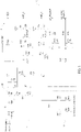
- FIG. 1 is a schematic diagram of a sensing circuit configured to awaken an electronic device in accordance with the disclosure.
- the terms "upper,” “lower,” “right,” “left,” “rear,” “front,” “vertical,” “horizontal,” “clockwise,” “counter-clockwise,” “interior,” “exterior” and derivatives thereof shall relate to the arrangement of the elements introduced in reference to FIG. 1 as viewed by an occupant of the vehicle shown.
- the various elements of the assemblies illustrated may assume various alternative orientations, except where expressly specified to the contrary.
- the specific devices and processes illustrated in the attached drawings, and described in the following specification are simply exemplary embodiments of the concepts defined in the appended claims. Hence, specific dimensions and other physical characteristics relating to the embodiments disclosed herein are not to be considered as limiting, unless the claims expressly state otherwise.
- a circuit 10 disclosed herein provides for an interface for an electrical device.
- Various embodiments of the disclosure may further provide for an interface in the form of the circuit 10 being disposed between the electrical device and a remote switch 12.
- the circuit 10 may correspond to a sensing circuit configured to limit a number of wires required to interface the electrical device while preventing power drainage into the circuit 10 during temporal periods of a standby mode of the electrical device.
- a microcontroller 14 in communication with the circuit 10 via a plurality of input/output (I/O) terminals 16 is idle.
- the circuit 10 is operable to prevent power usage by both the circuit 10 and the microcontroller 14 during the standby mode.
- the circuit 10 is further operable to activate the microcontroller 14 to sense at least one user input received by the remote switch 12. By maintaining a zero standby current in the standby mode, the sensing circuit 10 provides for an efficient activation of the microcontroller 14 to sense a user input to control the electrical device.
- the microcontroller 14 may correspond to any form of circuit or controller that may be operable to receive signals from the circuit 10 as described herein.
- the circuit 10 provides for an economical and effective design for a user interface configured to receive inputs to activate at least one output or routine of the electrical device.
- the electrical device may correspond to a wireless transmitter, for example a HOMELINK ® trainable wireless transmitter.
- the electrical device may utilize a transceiver to receive data corresponding to a variety of remote control devices.
- a remote control device may include a garage door opener control, a remote home security control, a lighting controller, etc.
- the electrical device may be operable to receive a control signal and program the signal to control an electronic device.
- the electrical device may be configured to learn and re-transmit one or more control signals configured to open/close a moving barrier, turn on/off lighting, activate/deactivate a security system, etc.
- the remote switch 12 may comprise two or more buttons or inputs corresponding to a user interface of the electrical device.
- a first switch S1 and a second switch S2 are configured to control the electrical device.
- a single button press e.g. depressing the first switch S1
- multiple button presses e.g. depressing switches S1 and S2
- Each of the inputs of the remote switch 12 is multiplexed on a control wire 18 corresponding to a single wire.
- the single wire interface between the circuit 10 and the switch 12 may provide for the switch 12 to be located away from the circuit 10 while allowing for the circuit 10 to receive signals efficiently through the control wire 18.
- the inputs of the remote switch 12 are encoded by providing a unique resistance value for each switch closure (e.g the switches S1 and S2). If a combination of the switches S1 and S2 are pressed simultaneously, an equivalent parallel resistance will be sensed.
- the circuit 10 is operable to output control signals having unique resistances in order to control the electrical device via the I/O terminals 16.
- the circuit 10 disclosed herein may differ from other circuits in that the unique architecture provides for approximately zero current draw in the idle mode while providing for a wakeup signal configured to activate a microcontroller 14 to sense a user input to control the electrical device.
- the circuit 10 is described in further detail to present various benefits and variations of the novel architecture disclosed herein.
- the circuit 10 is supplied power from a power supply in the form of a BATTERY.
- a first capacitor C1 and a second capacitor C2 provide radio frequency (RF) and electro-magnetic interference (EMI) protection as well as protection from transient spikes that may damage or cause improper operation of the circuit 10.
- the capacitors C1 and C2 are in connection with a battery line 20 conductively connected to the BATTERY.
- a first diode D1 provides reverse polarity protection on the battery line 20.
- a first transistor Q1 provides a switched and over-voltage protected output on a activation line VCLAMP in communication with the microcontroller 14.
- the first transistor Q1 is normally off, resulting in a nominal zero standby current.
- a transistor such as the first transistor Q1 may comprise three terminals: a base, a collector, and an emitter.
- the switches S1 and S2 are used to supply user inputs to the microcontroller 14.
- Resistors R8 and R7 are connected in series with switches S1 and S2 respectively. When any or all of the switches are closed, the first transistor Q1 is activated such that current flows from the battery through the first diode D1, each of the resistors R2 and R6, the closed switch and its associated resistor (e.g. R7 or R8).
- the activation of the first transistor Q1 provides protected battery power to the activation line VCLAMP, which powers the voltage regulator Vreg that supplies power to the microcontroller 14.
- the first resistor R1 is used to prevent unwanted activation of the first transistor Q1 due to potential leakage currents from the user input switches S1 and S2.
- the second resistor R2 limits a base current of the first transistor Q1.
- the sixth resistor R6 is used to provide for current sensing by the microcontroller 14 in response to user inputs into the switches S1 and S2.
- the microcontroller 14 is operable to identify an input into the switches corresponding to the first switch S1, the second switch S2, or a combination of the switches.
- the microcontroller 14 may sense a voltage or current corresponding to a first output node N1 and a second output node N2.
- the first output node N1 is in communication with the controller 14 via a first analog to digital (A/D) input AD_0 across a thirteenth resistor R13, and the second output node N2 is in communication with the controller 14 via a second A/D input AD_1 across a fourteenth resistor R14.
- A/D analog to digital
- the microcontroller 14 receives an activation signal and may be powered from a voltage regulator Vreg powered by the activation line VCLAMP.
- the microcontroller 14 boots up in response to the current received from the battery line 20 through the first transistor Q1.
- the microcontroller 14 is operable to determine the states of the switches S1 and S2 using the first A/D input AD_0 and the second A/D input AD_1 of the I/O terminals 16.
- the A/D inputs AD_0 and AD_1 are output from the circuit 10 to supply voltage to an A/D converter of the microcontroller 14.
- the voltage supplied to the A/D converter corresponds to the unique resistance value for each of the switches S1 and S2.
- the circuit 10 is operable to output control signals corresponding to the unique resistances to identify an input to one or more of the switches S1 and S2, and the microcontroller 14 is operable to identify the control signals received at the A/D converters AD 0 and AD 1.
- the circuit 10 may comprise a plurality of metal-oxide-semiconductor field-effect transistors (MOSFETs).
- MOSFETs metal-oxide-semiconductor field-effect transistors
- a first MOSFET M1 and a second MOSFET M2 are configured to be normally off to prevent standby power drain or activation of Q1 due to current flow into the A/D converter inputs of the unpowered microcontroller 14.
- a MOSFET such as the first MOSFET M1
- the gate and source voltages of the first MOSFET M1 and the second MOSFET M2 are equal as long as a fourth transistor Q4 is off or inactive.
- An eleventh resistor R11 pulls both gates to the source voltage of each of the MOSFETs M1 and M2.
- a third diode D3 may correspond to a Zener diode used to prevent excessive gate voltage from being applied to the MOSFETs M1 and M2.
- Gate resistors R9 and R10 are used to protect the MOSFETs M1 and M2 against unwanted activation due to RF energy.
- the microcontroller 14 can turn on the MOSFETS M1 and M2 by bringing a signal to an A/D enable input AD_ENABLE of the circuit 10 to a high signal.
- the MOSFETs M1 and M2 are configured to allow current to flow through a sixteenth resistor R16 and into a base of a fourth transistor Q4.
- the current flow at the base of the fourth transistor Q4 activates the gates of the MOSFETs M1 and M2 by pulling down the gate voltages and thereby allowing current to pass through the MOSFETs M1 and M2 to activate the A/D inputs AD_0 and AD_1.
- R15 may be optionally used to prevent unwanted operation of the fourth transistor Q4 due to small offset voltages that may be supplied to the circuit 10 from the AD_ENABLE line of the microcontroller 14.
- the microcontroller 14 can measure the voltages on the A/D inputs AD_0 and AD_1. If a switch S1 or S2 that has been previously activated is released, or the contacts of either switch S1 or S2 bounce while the MOSFETs M1 and M2 are turned on, approximately the full voltage of the of the power supply BATTERY will be applied to the drains of the MOSFETs M1 and M2.
- the microcontroller 14 may be operable to sense the full voltage from power supply VDD to verify that the A/D inputs AD0 and AD1 are stable.
- the microcontroller 14 is operable to verify that the signal supplied to the A/D inputs AD_0 and AD_1 are at a stable level less than the supply voltage for a predetermined period of time.
- various diodes, resistors, capacitors and other electrical components may be integrated in the circuit 10 and/or the microcontroller 14. Such components may provide for signal conditioning, voltage protection, reverse-polarity protection, RF and EMI protection, etc.
- the thirteenth resistor R13, the fourteenth resistor R14, and diodes D4-D7 are configured to protect the A/D inputs of the microcontroller 14 from over-voltage.
- Diodes D4-D7 may or may not be incorporated into the microcontroller 14.
- Capacitors C3 and C4 are noise filters configured to ensure stable A/D readings by the microcontroller 14. It is important to note that the specific components referenced in FIG. 1 including the models, resistances, capacitances, voltages and various additional properties of the specific components shown are intended as examples and should not be considered limiting to the disclosure.
- the resistance of the switch can be determined because the voltage drop across a known resistance R6 is proportional to the current through R6.
- the microcontroller 14 is operable to determine the resistance corresponding to an input into the first switch S1, the second switch S2, and a combination of the switches S1 and S2 as a switch resistance.
- the switch resistance may be calculated by dividing the voltage on second A/D input AD_1 by the current through the sixth resistor R6. Additionally, the ratio of the voltage difference between the voltage supplied to the first A/D input AD_0 and the second A/D input AD_1 can be compared to the voltage at second A/D input AD_1.
- the aforementioned comparisons may be utilized to determine the switch resistance and the corresponding input to one or more of the switches S1 and/or S2 due to the resistors R6, R7, and R8 having a predetermined relationship.
- the resistors R6, R7, and R8 are referred to herein as identifying resistors.
- the identifying resistors R6, R7, and R8 are termed such because the relationship of their resistance is utilized by the microcontroller 14 to identify which of the one or more switches S1 and S2 has received an input.
- the following illustrates an embodiment of the microcontroller 14 identifying an input received by the first switch S1, the second switch S2, or both switches S1 and S2.
- the resistance of the sixth resistor R6 is approximately equal to the resistance of the seventh resistor (R6 ⁇ R7)
- the resistance of the eighth resistor R8 is approximately equal to twice the resistance of the sixth resistor (R8 ⁇ 2 ⁇ R6).
- the disclosure provides for a circuit operable to receive a plurality of inputs from remote switches.
- the circuit 14 is operable to deliver signals that not only activate a microcontroller, but also may be used to identify a switch resistance corresponding to one or more inputs being received by a remote switch.
- the circuit may also be used for a single switch if it is necessary to distinguish a grounded switch line from a valid button press.
- the microcontroller 14 may activate a power enable input DO_PWR_ENABLE to the circuit 10 to high.
- the power enable input DO_PWR_ENABLE may provide for the base current to pass through an eighteenth resistor R18 to turn on a fifth transistor Q5.
- a seventeenth resistor R17 is optionally used to prevent unwanted operation of the fifth transistor Q5 due to small offset voltages on the power enable input DO_PWR_ENABLE.
- the base current from the first transistor Q1 will flow through a twelfth resistor R12 and the fifth transistor Q5 allowing the microcontroller 14 to keep the first transistor Q1 turned on even if the one or more switches S1 and/or S2 is released.
- the controller is operable to hold the activation line VCLAMP for a predetermined period of time to provide for operation of the microcontroller 14 and associated circuitry for a variety of applications.
- the second transistor Q2 is used to switch off or deactivate the activation line VCLAMP if excessive voltage is present on the power supply BATTERY.
- a second diode D2 which may correspond to a Zener diode, will begin to conduct at a predetermined voltage. The voltage conducted through the second diode may cause a current limited by R4 to flow through the base of Q2.
- the second transistor Q2 may activate shunting current around an emitter-base junction of the first transistor Q1. The shunting current around the emitter-base junction of the first transistor Q1 may result in turning the first transistor Q1 off, and thus, protecting the load (e.g. the voltage regulator Vreg and the microcontroller 14) on the activation line VCLAMP from excessive voltage on the battery line 20.
- the third transistor Q3 may be optionally utilized to allow the use of low voltage transistors at MOSFETs M1 and M2. If the third transistor Q3 is not used, the fifth resistor R5 may optionally be replaced by a short.
- the third resistor R3 is used to ensure that the second transistor Q2 is not activated by leakage current through the second diode D2 and to ensure that the second transistor Q2 only activates for over-voltage events.
- the third resistor R3 and the fifth resistor R5 can have a predetermined resistance value relationship.
- the second transistor Q2 may turn on slightly before the third transistor Q3 in order to ensure that the microcontroller 14 is never turned on with A/D inputs AD 0 and AD_1 held low.
- the fifth resistor R5 may be selected to have a lower resistance than the third resistor R3.
- the term "coupled” in all of its forms, couple, coupling, coupled, etc. generally means the joining of two components (electrical or mechanical) directly or indirectly to one another. Such joining may be stationary in nature or movable in nature. Such joining may be achieved with the two components (electrical or mechanical) and any additional intermediate members being integrally formed as a single unitary body with one another or with the two components. Such joining may be permanent in nature or may be removable or releasable in nature unless otherwise stated.
- elements shown as integrally formed may be constructed of multiple parts or elements shown as multiple parts may be integrally formed, the operation of the interfaces may be reversed or otherwise varied, the length or width of the structures and/or members or connector or other elements of the system may be varied, the nature or number of adjustment positions provided between the elements may be varied.
- the elements and/or assemblies of the system may be constructed from any of a wide variety of materials that provide sufficient strength or durability, in any of a wide variety of colors, textures, and combinations. Accordingly, all such modifications are intended to be included within the scope of the present innovations. Other substitutions, modifications, changes, and omissions may be made in the design, operating conditions, and arrangement of the desired and other exemplary embodiments without departing from the scope of the attached claims.
Landscapes
- Engineering & Computer Science (AREA)
- Theoretical Computer Science (AREA)
- Electronic Switches (AREA)
- Selective Calling Equipment (AREA)
Claims (11)
- Eine Erfassungsschaltung (10), die so konfiguriert ist, dass sie eine Steuerung (14) aktiviert, umfassend:einen Transistor (Q1), der so konfiguriert ist, dass er ein Aktivierungssignal an die Steuerung (14) ausgibt;eine Vielzahl von Schaltern (S1, S2), die in einem Fernschalter (12) in Verbindung mit einer Basis des Transistors angeordnet sind, wobei jeder der Schalter (S1, S2) verbunden ist mit einem Kennungswiderstand (R7, R8), wobei ein erster Schalter (S1) mit einem ersten Kennungswiderstand (R8) verbunden ist und ein zweiter Schalter (S2) mit einem zweiten Kennungswiderstand (R7) verbunden ist; undeinen ersten Ausgangsknoten (N1) und einen zweiten Ausgangsknoten (N2), die mit der Basis des Transistors (Q1) und jedem der Schalter (S1, S2) verbunden sind, undwobei der erste Ausgangsknoten (N1) und der zweite Ausgangsknoten (N2) über einen dritten Kennungswiderstand (R6) getrennt sind;wobei der erste Ausgangsknoten (N1) über einen ersten Analog-Digital-Eingang (AD_0) mit der Steuerung (14) in Verbindung steht und der zweite Ausgangsknoten (N2) über einen zweiten Analog-Digital-Eingang (AD_1) mit der Steuerung (14) in Verbindung steht;wobei der erste Analog-Digital-Eingang (AD_0) und der zweite Analog-Digital-Eingang von der Erfassungsschaltung (10) ausgegeben werden, um einen A/D-Wandler der Steuerung (14) mit Spannung zu versorgen;wobei der erste Ausgangsknoten (N1) und der zweite Ausgangsknoten (N2) dazu konfiguriert sind, eine charakteristische Spannung auszugeben, die einem Verhältnis jedes der Kennungswiderstände (R6, R7, R8) in Reaktion auf eine von jedem der Vielzahl von Schaltern (S1, S2) empfangene Eingabe entspricht;wobei die Kennungswiderstände (R6, R7, R8) eine vorbestimmte Beziehung zueinander aufweisen,wobei der Widerstand des dritten Kennungswiderstands (R6) ungefähr gleich dem Widerstand des zweiten Kennungswiderstands (R7) ist, und wobei der Widerstand des ersten Kennungswiderstands (R8) ungefähr gleich dem doppelten Widerstand des dritten Kennungswiderstands (R6) ist,wobei die vorbestimmte Beziehung zwischen dem Widerstand der Kennungswiderstände (R6, R7, R8) von der Steuerung (14) verwendet wird, um zu identifizieren, welcher der Vielzahl von Schaltern (S1, S2) ein Eingangssignal erhalten hat,wobei die Erfassungsschaltung ferner so konfiguriert ist, dass, wenn der zweite Schalter (S2) geschlossen ist, die Spannung am zweiten Analog-Digital-Eingang (AD_1) ungefähr gleich der Spannungsdifferenz zwischen dem ersten Analog-Digital-Eingang (AD_0) und dem zweiten Analog-Digital-Eingang (AD_1) ist,wobei, wenn der erste Schalter (S1) geschlossen ist, die Spannung am zweiten Analog-Digital-Eingang (AD_1) ungefähr gleich dem Doppelten der Spannungsdifferenz zwischen dem ersten Analog-Digital-Eingang (AD_0) und dem zweiten Analog-Digital-Eingang (AD_1) ist.
- Die Erfassungsschaltung (10) nach Anspruch 1, wobei der Transistor (Q1) dazu konfiguriert ist, einen Stromabfluss von einer Stromversorgung in Verbindung mit einem Emitter des Transistors (Q1) zu verhindern.
- Die Erfassungsschaltung (10) nach Anspruch 2, wobei die Stromversorgung dazu konfiguriert ist, das Aktivierungssignal als Reaktion auf die von jedem der Vielzahl von Schaltern (S1, S2) empfangene Eingabe zu liefern.
- Die Erfassungsschaltung (10) nach Anspruch 1, wobei der Fernschalter (12) über eine einzelne Steuerleitung (18) mit dem dritten Kennungswiderstand (R6) verbunden ist.
- Die Erfassungsschaltung (10) nach Anspruch 4, wobei die einzelne Steuerleitung dazu konfiguriert ist, ein Multiplexsignal vom Fernschalter (12) zu übertragen.
- Die Erfassungsschaltung (10) nach Anspruch 4, wobei die Steuerleitung (18) eine Fernverbindung mit dem Fernschalter (12) über einen einzigen leitenden Pfad bereitstellt.
- Die Erfassungsschaltung (10) nach Anspruch 1, wobei der Fernschalter (12) einer Benutzerschnittstelle entspricht, die so konfiguriert ist, dass sie als Reaktion auf eine Eingabe an jeden der Vielzahl von Schaltern (S1, S2) eindeutige Signale über die Steuerleitung (18) übermittelt.
- Die Erfassungsschaltung (10) nach Anspruch 7, wobei der Fernschalter (12) so konfiguriert ist, dass er jedes der eindeutigen Steuersignale über die Steuerleitung (18) übermittelt als Reaktion auf eine Eingabe in den ersten Schalter (S1), den zweiten Schalter (S2) und eine Eingabe in sowohl den ersten Schalter (S1) als auch den zweiten Schalter (S2).
- Die Erfassungsschaltung (10) nach Anspruch 1, wobei der erste Ausgangsknoten (N1) und der zweite Ausgangsknoten (N2) mit dem Steuergerät (14) in Verbindung stehen, das einen Sender umfasst, der konfiguriert ist, um eine entfernte elektronische Vorrichtung drahtlos zu steuern.
- Die Erfassungsschaltung (10) nach Anspruch 9, wobei jede der charakteristischen Spannungen so konfiguriert ist, dass sie mindestens eine von einer Kommunikationsfunktion und einer Trainingsfunktion für die Steuerung (14) steuert.
- Die Erfassungsschaltung (10) nach irgendeinem der Ansprüche von 1 bis 10, wobei die Erfassungsschaltung (10) so konfiguriert ist, dass sie die Steuerung (14) aus einer zeitlichen Periode eines Standby-Modus aktiviert.
Applications Claiming Priority (2)
| Application Number | Priority Date | Filing Date | Title |
|---|---|---|---|
| US201562118679P | 2015-02-20 | 2015-02-20 | |
| PCT/US2016/018491 WO2016134158A1 (en) | 2015-02-20 | 2016-02-18 | Resistor multiplexed switch wake-up circuit |
Publications (3)
| Publication Number | Publication Date |
|---|---|
| EP3259846A1 EP3259846A1 (de) | 2017-12-27 |
| EP3259846A4 EP3259846A4 (de) | 2018-02-28 |
| EP3259846B1 true EP3259846B1 (de) | 2022-03-30 |
Family
ID=56689167
Family Applications (1)
| Application Number | Title | Priority Date | Filing Date |
|---|---|---|---|
| EP16753068.2A Active EP3259846B1 (de) | 2015-02-20 | 2016-02-18 | Aufweckschaltung mit gemultiplextem widerstandsschalter |
Country Status (4)
| Country | Link |
|---|---|
| US (1) | US9954518B2 (de) |
| EP (1) | EP3259846B1 (de) |
| CN (1) | CN107251437B (de) |
| WO (1) | WO2016134158A1 (de) |
Families Citing this family (1)
| Publication number | Priority date | Publication date | Assignee | Title |
|---|---|---|---|---|
| CN112543017A (zh) * | 2020-12-02 | 2021-03-23 | 广州朗国电子科技有限公司 | 长连接且不影响功耗的电路 |
Citations (2)
| Publication number | Priority date | Publication date | Assignee | Title |
|---|---|---|---|---|
| EP0695041A2 (de) * | 1994-07-26 | 1996-01-31 | Nokia Mobile Phones Ltd. | Tastatur für Funktelefon |
| EP1006545B1 (de) * | 1998-12-04 | 2004-08-18 | Nokia Corporation | Vorrichtung zur Erzeugung von Eingabesignalen für ein elektronisches Gerät |
Family Cites Families (12)
| Publication number | Priority date | Publication date | Assignee | Title |
|---|---|---|---|---|
| DE3312153A1 (de) * | 1983-04-02 | 1984-10-04 | Grundig E.M.V. Elektro-Mechanische Versuchsanstalt Max Grundig & Co KG, 8510 Fürth | Verfahren und schaltungsanordnung zur tastenabfrage |
| US5760625A (en) * | 1995-10-03 | 1998-06-02 | Ford Motor Company | Low cost microcomputer power supply with power on reset and low voltage inhibit functionality |
| US6181255B1 (en) * | 1997-02-27 | 2001-01-30 | The Chamberlain Group, Inc. | Multi-frequency radio frequency transmitter with code learning capability |
| US6005499A (en) * | 1997-07-21 | 1999-12-21 | Toshiba America Information Systems, Inc. | Systems and methods for generating key press status messages within telecommunications systems or other networks |
| JP3924179B2 (ja) * | 2002-02-12 | 2007-06-06 | ローム株式会社 | D/a変換回路およびこれを用いる有機el駆動回路 |
| KR100634169B1 (ko) * | 2004-03-10 | 2006-10-16 | 삼성전자주식회사 | 가변형 기준레벨 발생 기능을 가진 센스 앰프 및 그 방법 |
| US7248195B2 (en) * | 2005-11-30 | 2007-07-24 | Symbol Technologies, Inc. | Methods and apparatus for multiplexed digital inputs using an analog-to-digital converter |
| US8384513B2 (en) | 2006-01-03 | 2013-02-26 | Johnson Controls Technology Company | Transmitter and method for transmitting an RF control signal |
| US7486106B1 (en) | 2006-03-24 | 2009-02-03 | Altera Corporation | CPLD for multi-wire keyboard decode with timed power control circuit |
| RU65663U1 (ru) * | 2007-03-12 | 2007-08-10 | Открытое акционерное общество "Научно-производственное предприятие "Рубин" (ОАО "НПП "Рубин") | Устройство преобразования код-аналог |
| KR101357759B1 (ko) * | 2011-04-28 | 2014-02-03 | 에스케이하이닉스 주식회사 | 퓨즈회로를 포함하는 반도체 집적회로 및 반도체 메모리 장치 |
| CN202856608U (zh) * | 2012-05-24 | 2013-04-03 | 意法半导体研发(深圳)有限公司 | 用于功率驱动的电路 |
-
2016
- 2016-02-18 CN CN201680010518.0A patent/CN107251437B/zh active Active
- 2016-02-18 WO PCT/US2016/018491 patent/WO2016134158A1/en not_active Ceased
- 2016-02-18 US US15/046,982 patent/US9954518B2/en active Active
- 2016-02-18 EP EP16753068.2A patent/EP3259846B1/de active Active
Patent Citations (2)
| Publication number | Priority date | Publication date | Assignee | Title |
|---|---|---|---|---|
| EP0695041A2 (de) * | 1994-07-26 | 1996-01-31 | Nokia Mobile Phones Ltd. | Tastatur für Funktelefon |
| EP1006545B1 (de) * | 1998-12-04 | 2004-08-18 | Nokia Corporation | Vorrichtung zur Erzeugung von Eingabesignalen für ein elektronisches Gerät |
Also Published As
| Publication number | Publication date |
|---|---|
| CN107251437A (zh) | 2017-10-13 |
| US20160248416A1 (en) | 2016-08-25 |
| WO2016134158A1 (en) | 2016-08-25 |
| EP3259846A1 (de) | 2017-12-27 |
| CN107251437B (zh) | 2020-09-25 |
| US9954518B2 (en) | 2018-04-24 |
| EP3259846A4 (de) | 2018-02-28 |
Similar Documents
| Publication | Publication Date | Title |
|---|---|---|
| US7023215B2 (en) | Field effect sensor two wire interconnect method and apparatus | |
| US5940000A (en) | Trainable transmitter security circuit | |
| US8839557B2 (en) | Automatic door closer | |
| US20170005718A1 (en) | Wireless Relay | |
| EP3259846B1 (de) | Aufweckschaltung mit gemultiplextem widerstandsschalter | |
| KR101821327B1 (ko) | 암전류 저감이 가능한 입력 회로 | |
| KR101714320B1 (ko) | 스위치 감시 회로 | |
| EP2309088A3 (de) | Schaltkreis für elektrisches Fenster. | |
| KR102709118B1 (ko) | 활성화 신호에 반응하여 회로 장치에 의해 컴퓨터 유닛을 활성화하기 위한 방법 | |
| US20110148565A1 (en) | Monitoring system and input and output device | |
| JP3290044B2 (ja) | 無線通信機 | |
| JPWO2015068342A1 (ja) | 端末機および無線通信システム | |
| US8289128B2 (en) | Monitoring system and input/output device thereof | |
| EP1763138A3 (de) | Fahrzeugschaltkreis | |
| US20210385568A1 (en) | Keyless control device and earphone | |
| JP2012156701A (ja) | 送信機 | |
| US20010020801A1 (en) | Configuration for triggering a restraint device in a motor vehicle | |
| CN115298067A (zh) | 用于车辆的控制电路及控制单元 | |
| NZ762993A (en) | Electronic lockset having mode selection | |
| AU711360B2 (en) | Reprogrammable battery | |
| JP3632954B2 (ja) | ドライバ回路 | |
| TW200739331A (en) | Fan system and power monitoring device thereof | |
| WO2005036184A3 (de) | Elektronische schaltungsanordnung zum anschluss mindestens eines aktiven drehzahlsensors, insbesondere bei nutzfahrzeugen | |
| KR200349538Y1 (ko) | 비상제어회로가 구비된 디지털도어록장치 | |
| KR20210085774A (ko) | 대기 상태에서 부가 전원 공급이 가능한 출입 제어 시스템 |
Legal Events
| Date | Code | Title | Description |
|---|---|---|---|
| STAA | Information on the status of an ep patent application or granted ep patent |
Free format text: STATUS: THE INTERNATIONAL PUBLICATION HAS BEEN MADE |
|
| PUAI | Public reference made under article 153(3) epc to a published international application that has entered the european phase |
Free format text: ORIGINAL CODE: 0009012 |
|
| STAA | Information on the status of an ep patent application or granted ep patent |
Free format text: STATUS: REQUEST FOR EXAMINATION WAS MADE |
|
| 17P | Request for examination filed |
Effective date: 20170831 |
|
| AK | Designated contracting states |
Kind code of ref document: A1 Designated state(s): AL AT BE BG CH CY CZ DE DK EE ES FI FR GB GR HR HU IE IS IT LI LT LU LV MC MK MT NL NO PL PT RO RS SE SI SK SM TR |
|
| AX | Request for extension of the european patent |
Extension state: BA ME |
|
| REG | Reference to a national code |
Ref country code: DE Ref legal event code: R079 Ref document number: 602016070509 Country of ref document: DE Free format text: PREVIOUS MAIN CLASS: H03M0001800000 Ipc: H03M0011240000 |
|
| A4 | Supplementary search report drawn up and despatched |
Effective date: 20180126 |
|
| RIC1 | Information provided on ipc code assigned before grant |
Ipc: H03M 11/24 20060101AFI20180122BHEP Ipc: H03K 17/22 20060101ALI20180122BHEP |
|
| DAV | Request for validation of the european patent (deleted) | ||
| DAX | Request for extension of the european patent (deleted) | ||
| STAA | Information on the status of an ep patent application or granted ep patent |
Free format text: STATUS: EXAMINATION IS IN PROGRESS |
|
| 17Q | First examination report despatched |
Effective date: 20200414 |
|
| GRAP | Despatch of communication of intention to grant a patent |
Free format text: ORIGINAL CODE: EPIDOSNIGR1 |
|
| STAA | Information on the status of an ep patent application or granted ep patent |
Free format text: STATUS: GRANT OF PATENT IS INTENDED |
|
| INTG | Intention to grant announced |
Effective date: 20210601 |
|
| GRAJ | Information related to disapproval of communication of intention to grant by the applicant or resumption of examination proceedings by the epo deleted |
Free format text: ORIGINAL CODE: EPIDOSDIGR1 |
|
| STAA | Information on the status of an ep patent application or granted ep patent |
Free format text: STATUS: EXAMINATION IS IN PROGRESS |
|
| INTC | Intention to grant announced (deleted) | ||
| GRAP | Despatch of communication of intention to grant a patent |
Free format text: ORIGINAL CODE: EPIDOSNIGR1 |
|
| STAA | Information on the status of an ep patent application or granted ep patent |
Free format text: STATUS: GRANT OF PATENT IS INTENDED |
|
| INTG | Intention to grant announced |
Effective date: 20211015 |
|
| GRAS | Grant fee paid |
Free format text: ORIGINAL CODE: EPIDOSNIGR3 |
|
| GRAA | (expected) grant |
Free format text: ORIGINAL CODE: 0009210 |
|
| STAA | Information on the status of an ep patent application or granted ep patent |
Free format text: STATUS: THE PATENT HAS BEEN GRANTED |
|
| AK | Designated contracting states |
Kind code of ref document: B1 Designated state(s): AL AT BE BG CH CY CZ DE DK EE ES FI FR GB GR HR HU IE IS IT LI LT LU LV MC MK MT NL NO PL PT RO RS SE SI SK SM TR |
|
| REG | Reference to a national code |
Ref country code: GB Ref legal event code: FG4D |
|
| REG | Reference to a national code |
Ref country code: CH Ref legal event code: EP |
|
| REG | Reference to a national code |
Ref country code: AT Ref legal event code: REF Ref document number: 1480134 Country of ref document: AT Kind code of ref document: T Effective date: 20220415 |
|
| REG | Reference to a national code |
Ref country code: DE Ref legal event code: R096 Ref document number: 602016070509 Country of ref document: DE |
|
| REG | Reference to a national code |
Ref country code: IE Ref legal event code: FG4D |
|
| REG | Reference to a national code |
Ref country code: LT Ref legal event code: MG9D |
|
| PG25 | Lapsed in a contracting state [announced via postgrant information from national office to epo] |
Ref country code: SE Free format text: LAPSE BECAUSE OF FAILURE TO SUBMIT A TRANSLATION OF THE DESCRIPTION OR TO PAY THE FEE WITHIN THE PRESCRIBED TIME-LIMIT Effective date: 20220330 Ref country code: RS Free format text: LAPSE BECAUSE OF FAILURE TO SUBMIT A TRANSLATION OF THE DESCRIPTION OR TO PAY THE FEE WITHIN THE PRESCRIBED TIME-LIMIT Effective date: 20220330 Ref country code: NO Free format text: LAPSE BECAUSE OF FAILURE TO SUBMIT A TRANSLATION OF THE DESCRIPTION OR TO PAY THE FEE WITHIN THE PRESCRIBED TIME-LIMIT Effective date: 20220630 Ref country code: LT Free format text: LAPSE BECAUSE OF FAILURE TO SUBMIT A TRANSLATION OF THE DESCRIPTION OR TO PAY THE FEE WITHIN THE PRESCRIBED TIME-LIMIT Effective date: 20220330 Ref country code: HR Free format text: LAPSE BECAUSE OF FAILURE TO SUBMIT A TRANSLATION OF THE DESCRIPTION OR TO PAY THE FEE WITHIN THE PRESCRIBED TIME-LIMIT Effective date: 20220330 Ref country code: BG Free format text: LAPSE BECAUSE OF FAILURE TO SUBMIT A TRANSLATION OF THE DESCRIPTION OR TO PAY THE FEE WITHIN THE PRESCRIBED TIME-LIMIT Effective date: 20220630 |
|
| REG | Reference to a national code |
Ref country code: NL Ref legal event code: MP Effective date: 20220330 |
|
| REG | Reference to a national code |
Ref country code: AT Ref legal event code: MK05 Ref document number: 1480134 Country of ref document: AT Kind code of ref document: T Effective date: 20220330 |
|
| PG25 | Lapsed in a contracting state [announced via postgrant information from national office to epo] |
Ref country code: LV Free format text: LAPSE BECAUSE OF FAILURE TO SUBMIT A TRANSLATION OF THE DESCRIPTION OR TO PAY THE FEE WITHIN THE PRESCRIBED TIME-LIMIT Effective date: 20220330 Ref country code: GR Free format text: LAPSE BECAUSE OF FAILURE TO SUBMIT A TRANSLATION OF THE DESCRIPTION OR TO PAY THE FEE WITHIN THE PRESCRIBED TIME-LIMIT Effective date: 20220701 Ref country code: FI Free format text: LAPSE BECAUSE OF FAILURE TO SUBMIT A TRANSLATION OF THE DESCRIPTION OR TO PAY THE FEE WITHIN THE PRESCRIBED TIME-LIMIT Effective date: 20220330 |
|
| PG25 | Lapsed in a contracting state [announced via postgrant information from national office to epo] |
Ref country code: NL Free format text: LAPSE BECAUSE OF FAILURE TO SUBMIT A TRANSLATION OF THE DESCRIPTION OR TO PAY THE FEE WITHIN THE PRESCRIBED TIME-LIMIT Effective date: 20220330 |
|
| PG25 | Lapsed in a contracting state [announced via postgrant information from national office to epo] |
Ref country code: SM Free format text: LAPSE BECAUSE OF FAILURE TO SUBMIT A TRANSLATION OF THE DESCRIPTION OR TO PAY THE FEE WITHIN THE PRESCRIBED TIME-LIMIT Effective date: 20220330 Ref country code: SK Free format text: LAPSE BECAUSE OF FAILURE TO SUBMIT A TRANSLATION OF THE DESCRIPTION OR TO PAY THE FEE WITHIN THE PRESCRIBED TIME-LIMIT Effective date: 20220330 Ref country code: RO Free format text: LAPSE BECAUSE OF FAILURE TO SUBMIT A TRANSLATION OF THE DESCRIPTION OR TO PAY THE FEE WITHIN THE PRESCRIBED TIME-LIMIT Effective date: 20220330 Ref country code: PT Free format text: LAPSE BECAUSE OF FAILURE TO SUBMIT A TRANSLATION OF THE DESCRIPTION OR TO PAY THE FEE WITHIN THE PRESCRIBED TIME-LIMIT Effective date: 20220801 Ref country code: ES Free format text: LAPSE BECAUSE OF FAILURE TO SUBMIT A TRANSLATION OF THE DESCRIPTION OR TO PAY THE FEE WITHIN THE PRESCRIBED TIME-LIMIT Effective date: 20220330 Ref country code: EE Free format text: LAPSE BECAUSE OF FAILURE TO SUBMIT A TRANSLATION OF THE DESCRIPTION OR TO PAY THE FEE WITHIN THE PRESCRIBED TIME-LIMIT Effective date: 20220330 Ref country code: CZ Free format text: LAPSE BECAUSE OF FAILURE TO SUBMIT A TRANSLATION OF THE DESCRIPTION OR TO PAY THE FEE WITHIN THE PRESCRIBED TIME-LIMIT Effective date: 20220330 Ref country code: AT Free format text: LAPSE BECAUSE OF FAILURE TO SUBMIT A TRANSLATION OF THE DESCRIPTION OR TO PAY THE FEE WITHIN THE PRESCRIBED TIME-LIMIT Effective date: 20220330 |
|
| PG25 | Lapsed in a contracting state [announced via postgrant information from national office to epo] |
Ref country code: PL Free format text: LAPSE BECAUSE OF FAILURE TO SUBMIT A TRANSLATION OF THE DESCRIPTION OR TO PAY THE FEE WITHIN THE PRESCRIBED TIME-LIMIT Effective date: 20220330 Ref country code: IS Free format text: LAPSE BECAUSE OF FAILURE TO SUBMIT A TRANSLATION OF THE DESCRIPTION OR TO PAY THE FEE WITHIN THE PRESCRIBED TIME-LIMIT Effective date: 20220730 Ref country code: AL Free format text: LAPSE BECAUSE OF FAILURE TO SUBMIT A TRANSLATION OF THE DESCRIPTION OR TO PAY THE FEE WITHIN THE PRESCRIBED TIME-LIMIT Effective date: 20220330 |
|
| REG | Reference to a national code |
Ref country code: DE Ref legal event code: R097 Ref document number: 602016070509 Country of ref document: DE |
|
| PG25 | Lapsed in a contracting state [announced via postgrant information from national office to epo] |
Ref country code: DK Free format text: LAPSE BECAUSE OF FAILURE TO SUBMIT A TRANSLATION OF THE DESCRIPTION OR TO PAY THE FEE WITHIN THE PRESCRIBED TIME-LIMIT Effective date: 20220330 |
|
| PLBE | No opposition filed within time limit |
Free format text: ORIGINAL CODE: 0009261 |
|
| STAA | Information on the status of an ep patent application or granted ep patent |
Free format text: STATUS: NO OPPOSITION FILED WITHIN TIME LIMIT |
|
| 26N | No opposition filed |
Effective date: 20230103 |
|
| PG25 | Lapsed in a contracting state [announced via postgrant information from national office to epo] |
Ref country code: SI Free format text: LAPSE BECAUSE OF FAILURE TO SUBMIT A TRANSLATION OF THE DESCRIPTION OR TO PAY THE FEE WITHIN THE PRESCRIBED TIME-LIMIT Effective date: 20220330 |
|
| P01 | Opt-out of the competence of the unified patent court (upc) registered |
Effective date: 20230503 |
|
| PG25 | Lapsed in a contracting state [announced via postgrant information from national office to epo] |
Ref country code: IT Free format text: LAPSE BECAUSE OF FAILURE TO SUBMIT A TRANSLATION OF THE DESCRIPTION OR TO PAY THE FEE WITHIN THE PRESCRIBED TIME-LIMIT Effective date: 20220330 |
|
| PG25 | Lapsed in a contracting state [announced via postgrant information from national office to epo] |
Ref country code: MC Free format text: LAPSE BECAUSE OF FAILURE TO SUBMIT A TRANSLATION OF THE DESCRIPTION OR TO PAY THE FEE WITHIN THE PRESCRIBED TIME-LIMIT Effective date: 20220330 |
|
| REG | Reference to a national code |
Ref country code: CH Ref legal event code: PL |
|
| REG | Reference to a national code |
Ref country code: BE Ref legal event code: MM Effective date: 20230228 |
|
| PG25 | Lapsed in a contracting state [announced via postgrant information from national office to epo] |
Ref country code: LU Free format text: LAPSE BECAUSE OF NON-PAYMENT OF DUE FEES Effective date: 20230218 Ref country code: LI Free format text: LAPSE BECAUSE OF NON-PAYMENT OF DUE FEES Effective date: 20230228 Ref country code: CH Free format text: LAPSE BECAUSE OF NON-PAYMENT OF DUE FEES Effective date: 20230228 |
|
| REG | Reference to a national code |
Ref country code: IE Ref legal event code: MM4A |
|
| PG25 | Lapsed in a contracting state [announced via postgrant information from national office to epo] |
Ref country code: IE Free format text: LAPSE BECAUSE OF NON-PAYMENT OF DUE FEES Effective date: 20230218 |
|
| PG25 | Lapsed in a contracting state [announced via postgrant information from national office to epo] |
Ref country code: BE Free format text: LAPSE BECAUSE OF NON-PAYMENT OF DUE FEES Effective date: 20230228 |
|
| PGFP | Annual fee paid to national office [announced via postgrant information from national office to epo] |
Ref country code: FR Payment date: 20250122 Year of fee payment: 10 |
|
| PGFP | Annual fee paid to national office [announced via postgrant information from national office to epo] |
Ref country code: GB Payment date: 20250123 Year of fee payment: 10 |
|
| PG25 | Lapsed in a contracting state [announced via postgrant information from national office to epo] |
Ref country code: CY Free format text: LAPSE BECAUSE OF FAILURE TO SUBMIT A TRANSLATION OF THE DESCRIPTION OR TO PAY THE FEE WITHIN THE PRESCRIBED TIME-LIMIT; INVALID AB INITIO Effective date: 20160218 |
|
| PG25 | Lapsed in a contracting state [announced via postgrant information from national office to epo] |
Ref country code: HU Free format text: LAPSE BECAUSE OF FAILURE TO SUBMIT A TRANSLATION OF THE DESCRIPTION OR TO PAY THE FEE WITHIN THE PRESCRIBED TIME-LIMIT; INVALID AB INITIO Effective date: 20160218 |
|
| PG25 | Lapsed in a contracting state [announced via postgrant information from national office to epo] |
Ref country code: TR Free format text: LAPSE BECAUSE OF FAILURE TO SUBMIT A TRANSLATION OF THE DESCRIPTION OR TO PAY THE FEE WITHIN THE PRESCRIBED TIME-LIMIT Effective date: 20220330 |
|
| PGFP | Annual fee paid to national office [announced via postgrant information from national office to epo] |
Ref country code: DE Payment date: 20260121 Year of fee payment: 11 |