EP3258745A1 - Circuit de stabilisation de tension d'entrée de lampe de combinaison arrière, lampe de combinaison arrière et véhicule - Google Patents
Circuit de stabilisation de tension d'entrée de lampe de combinaison arrière, lampe de combinaison arrière et véhicule Download PDFInfo
- Publication number
- EP3258745A1 EP3258745A1 EP17164959.3A EP17164959A EP3258745A1 EP 3258745 A1 EP3258745 A1 EP 3258745A1 EP 17164959 A EP17164959 A EP 17164959A EP 3258745 A1 EP3258745 A1 EP 3258745A1
- Authority
- EP
- European Patent Office
- Prior art keywords
- vehicle
- voltage
- oleds
- unit
- converter
- Prior art date
- Legal status (The legal status is an assumption and is not a legal conclusion. Google has not performed a legal analysis and makes no representation as to the accuracy of the status listed.)
- Granted
Links
- 230000006641 stabilisation Effects 0.000 title claims abstract description 51
- 238000011105 stabilization Methods 0.000 title claims abstract description 51
- 230000003287 optical effect Effects 0.000 claims abstract description 36
- 239000003990 capacitor Substances 0.000 claims description 15
- 230000001012 protector Effects 0.000 claims description 12
- 230000002159 abnormal effect Effects 0.000 claims description 5
- 238000004891 communication Methods 0.000 description 25
- 230000006870 function Effects 0.000 description 13
- 238000005286 illumination Methods 0.000 description 7
- 230000001133 acceleration Effects 0.000 description 6
- 239000000725 suspension Substances 0.000 description 6
- 238000010586 diagram Methods 0.000 description 5
- 230000008901 benefit Effects 0.000 description 4
- 230000008859 change Effects 0.000 description 2
- 230000007423 decrease Effects 0.000 description 2
- 239000000446 fuel Substances 0.000 description 2
- 239000004973 liquid crystal related substance Substances 0.000 description 2
- 238000012545 processing Methods 0.000 description 2
- 230000005236 sound signal Effects 0.000 description 2
- 239000010409 thin film Substances 0.000 description 2
- 238000012876 topography Methods 0.000 description 2
- XUIMIQQOPSSXEZ-UHFFFAOYSA-N Silicon Chemical compound [Si] XUIMIQQOPSSXEZ-UHFFFAOYSA-N 0.000 description 1
- 238000004378 air conditioning Methods 0.000 description 1
- 238000003491 array Methods 0.000 description 1
- 230000005540 biological transmission Effects 0.000 description 1
- 238000002485 combustion reaction Methods 0.000 description 1
- 230000036461 convulsion Effects 0.000 description 1
- 238000013500 data storage Methods 0.000 description 1
- 238000001514 detection method Methods 0.000 description 1
- 230000000694 effects Effects 0.000 description 1
- 238000005516 engineering process Methods 0.000 description 1
- 239000002803 fossil fuel Substances 0.000 description 1
- 230000014509 gene expression Effects 0.000 description 1
- 239000011521 glass Substances 0.000 description 1
- 238000010438 heat treatment Methods 0.000 description 1
- 238000000034 method Methods 0.000 description 1
- 238000012986 modification Methods 0.000 description 1
- 230000004048 modification Effects 0.000 description 1
- 230000007935 neutral effect Effects 0.000 description 1
- 230000008569 process Effects 0.000 description 1
- 238000011160 research Methods 0.000 description 1
- 229910052710 silicon Inorganic materials 0.000 description 1
- 239000010703 silicon Substances 0.000 description 1
- 239000007787 solid Substances 0.000 description 1
- XLYOFNOQVPJJNP-UHFFFAOYSA-N water Substances O XLYOFNOQVPJJNP-UHFFFAOYSA-N 0.000 description 1
Images


Classifications
-
- B—PERFORMING OPERATIONS; TRANSPORTING
- B60—VEHICLES IN GENERAL
- B60Q—ARRANGEMENT OF SIGNALLING OR LIGHTING DEVICES, THE MOUNTING OR SUPPORTING THEREOF OR CIRCUITS THEREFOR, FOR VEHICLES IN GENERAL
- B60Q1/00—Arrangement of optical signalling or lighting devices, the mounting or supporting thereof or circuits therefor
- B60Q1/26—Arrangement of optical signalling or lighting devices, the mounting or supporting thereof or circuits therefor the devices being primarily intended to indicate the vehicle, or parts thereof, or to give signals, to other traffic
-
- H—ELECTRICITY
- H05—ELECTRIC TECHNIQUES NOT OTHERWISE PROVIDED FOR
- H05B—ELECTRIC HEATING; ELECTRIC LIGHT SOURCES NOT OTHERWISE PROVIDED FOR; CIRCUIT ARRANGEMENTS FOR ELECTRIC LIGHT SOURCES, IN GENERAL
- H05B45/00—Circuit arrangements for operating light-emitting diodes [LED]
- H05B45/40—Details of LED load circuits
- H05B45/44—Details of LED load circuits with an active control inside an LED matrix
- H05B45/46—Details of LED load circuits with an active control inside an LED matrix having LEDs disposed in parallel lines
-
- B—PERFORMING OPERATIONS; TRANSPORTING
- B60—VEHICLES IN GENERAL
- B60Q—ARRANGEMENT OF SIGNALLING OR LIGHTING DEVICES, THE MOUNTING OR SUPPORTING THEREOF OR CIRCUITS THEREFOR, FOR VEHICLES IN GENERAL
- B60Q1/00—Arrangement of optical signalling or lighting devices, the mounting or supporting thereof or circuits therefor
- B60Q1/26—Arrangement of optical signalling or lighting devices, the mounting or supporting thereof or circuits therefor the devices being primarily intended to indicate the vehicle, or parts thereof, or to give signals, to other traffic
- B60Q1/30—Arrangement of optical signalling or lighting devices, the mounting or supporting thereof or circuits therefor the devices being primarily intended to indicate the vehicle, or parts thereof, or to give signals, to other traffic for indicating rear of vehicle, e.g. by means of reflecting surfaces
-
- B—PERFORMING OPERATIONS; TRANSPORTING
- B60—VEHICLES IN GENERAL
- B60Q—ARRANGEMENT OF SIGNALLING OR LIGHTING DEVICES, THE MOUNTING OR SUPPORTING THEREOF OR CIRCUITS THEREFOR, FOR VEHICLES IN GENERAL
- B60Q1/00—Arrangement of optical signalling or lighting devices, the mounting or supporting thereof or circuits therefor
- B60Q1/26—Arrangement of optical signalling or lighting devices, the mounting or supporting thereof or circuits therefor the devices being primarily intended to indicate the vehicle, or parts thereof, or to give signals, to other traffic
- B60Q1/34—Arrangement of optical signalling or lighting devices, the mounting or supporting thereof or circuits therefor the devices being primarily intended to indicate the vehicle, or parts thereof, or to give signals, to other traffic for indicating change of drive direction
- B60Q1/38—Arrangement of optical signalling or lighting devices, the mounting or supporting thereof or circuits therefor the devices being primarily intended to indicate the vehicle, or parts thereof, or to give signals, to other traffic for indicating change of drive direction using immovably-mounted light sources, e.g. fixed flashing lamps
-
- B—PERFORMING OPERATIONS; TRANSPORTING
- B60—VEHICLES IN GENERAL
- B60Q—ARRANGEMENT OF SIGNALLING OR LIGHTING DEVICES, THE MOUNTING OR SUPPORTING THEREOF OR CIRCUITS THEREFOR, FOR VEHICLES IN GENERAL
- B60Q1/00—Arrangement of optical signalling or lighting devices, the mounting or supporting thereof or circuits therefor
- B60Q1/26—Arrangement of optical signalling or lighting devices, the mounting or supporting thereof or circuits therefor the devices being primarily intended to indicate the vehicle, or parts thereof, or to give signals, to other traffic
- B60Q1/44—Arrangement of optical signalling or lighting devices, the mounting or supporting thereof or circuits therefor the devices being primarily intended to indicate the vehicle, or parts thereof, or to give signals, to other traffic for indicating braking action or preparation for braking, e.g. by detection of the foot approaching the brake pedal
-
- F—MECHANICAL ENGINEERING; LIGHTING; HEATING; WEAPONS; BLASTING
- F21—LIGHTING
- F21S—NON-PORTABLE LIGHTING DEVICES; SYSTEMS THEREOF; VEHICLE LIGHTING DEVICES SPECIALLY ADAPTED FOR VEHICLE EXTERIORS
- F21S43/00—Signalling devices specially adapted for vehicle exteriors, e.g. brake lamps, direction indicator lights or reversing lights
- F21S43/10—Signalling devices specially adapted for vehicle exteriors, e.g. brake lamps, direction indicator lights or reversing lights characterised by the light source
- F21S43/13—Signalling devices specially adapted for vehicle exteriors, e.g. brake lamps, direction indicator lights or reversing lights characterised by the light source characterised by the type of light source
- F21S43/14—Light emitting diodes [LED]
- F21S43/145—Surface emitters, e.g. organic light emitting diodes [OLED]
-
- H—ELECTRICITY
- H05—ELECTRIC TECHNIQUES NOT OTHERWISE PROVIDED FOR
- H05B—ELECTRIC HEATING; ELECTRIC LIGHT SOURCES NOT OTHERWISE PROVIDED FOR; CIRCUIT ARRANGEMENTS FOR ELECTRIC LIGHT SOURCES, IN GENERAL
- H05B45/00—Circuit arrangements for operating light-emitting diodes [LED]
- H05B45/60—Circuit arrangements for operating LEDs comprising organic material, e.g. for operating organic light-emitting diodes [OLED] or polymer light-emitting diodes [PLED]
-
- B—PERFORMING OPERATIONS; TRANSPORTING
- B60—VEHICLES IN GENERAL
- B60Q—ARRANGEMENT OF SIGNALLING OR LIGHTING DEVICES, THE MOUNTING OR SUPPORTING THEREOF OR CIRCUITS THEREFOR, FOR VEHICLES IN GENERAL
- B60Q2400/00—Special features or arrangements of exterior signal lamps for vehicles
- B60Q2400/20—Multi-color single source or LED matrix, e.g. yellow blinker and red brake lamp generated by single lamp
-
- Y—GENERAL TAGGING OF NEW TECHNOLOGICAL DEVELOPMENTS; GENERAL TAGGING OF CROSS-SECTIONAL TECHNOLOGIES SPANNING OVER SEVERAL SECTIONS OF THE IPC; TECHNICAL SUBJECTS COVERED BY FORMER USPC CROSS-REFERENCE ART COLLECTIONS [XRACs] AND DIGESTS
- Y02—TECHNOLOGIES OR APPLICATIONS FOR MITIGATION OR ADAPTATION AGAINST CLIMATE CHANGE
- Y02B—CLIMATE CHANGE MITIGATION TECHNOLOGIES RELATED TO BUILDINGS, e.g. HOUSING, HOUSE APPLIANCES OR RELATED END-USER APPLICATIONS
- Y02B20/00—Energy efficient lighting technologies, e.g. halogen lamps or gas discharge lamps
- Y02B20/30—Semiconductor lamps, e.g. solid state lamps [SSL] light emitting diodes [LED] or organic LED [OLED]
Definitions
- the present invention relates to an input voltage stabilization circuit for a rear combination lamp in a vehicle, the rear combination lamp, and the vehicle.
- a vehicle refers to a device that carries a passenger in a passenger-intended direction.
- a car is a major example of the vehicle.
- a vehicle is equipped with various sensors and electronic devices.
- ADAS Advanced Driver Assistance System
- autonomous vehicles are under active study to increase the driving convenience of users.
- the vehicle has a plurality of lamps.
- a Light Emitting Diode (LED), a Laser Diode (LD), or the like has recently been adopted as a light source for such a lamp.
- LEDs and LDs are suitable as a light source for a head lamp that should ensure visibility for a driver, due to their large light intensity.
- the large light intensity may be an obstacle to a driver of another vehicle, which makes LEDs and LDs unsuitable for a read combination lamp that provides various signals to other vehicles.
- OLED Organic Light Emitting Diode
- an object of the present invention is to provide an input voltage stabilization circuit in a rear combination lamp, for supplying a stable voltage to a plurality of Organic Light Emitting Diodes (OLEDs) included in the rear combination lamp.
- OLEDs Organic Light Emitting Diodes
- Another object of the present invention is to provide a rear combination lamp including the input voltage stabilization circuit.
- Another object of the present invention is to provide a vehicle including the rear combination lamp or the input voltage stabilization circuit of the rear combination lamp.
- an input voltage stabilization circuit for a rear combination lamp includes an optical output unit including a plurality of Organic Light Emitting Diodes (OELDs), a Direct Current to Direct Current (DC-DC) converter configured to supply an output voltage for driving the plurality of OLEDs by raising or lowering a voltage of a main power supplied by a vehicle battery, and a feedback unit configured to provide information about a highest of voltage values required for the plurality of individual OLEDs, as a feedback to the DC-DC converter.
- the DC-DC converter adjusts the output voltage based on the feedback.
- the term 'have', 'may have', 'include', or 'may include' signifies the presence of a specific feature, number, operation, component, or part, or their combinations, not excluding the presence or addition of one or more other features, numbers, operations, components, or parts, or their combinations.
- 'vehicle' used in the present disclosure may cover a car and a motorbike in concept.
- the following description is given with the appreciation that a vehicle is a car, by way of example.
- a vehicle may be any of an internal combustion vehicle equipped with an engine as a power source, a hybrid vehicle equipped with an engine and an electrical motor as power sources, an electric vehicle equipped with an electrical motor as a power source, and the like.
- the left of a vehicle means the left of a traveling direction of the vehicle
- the right of the vehicle means the right of the traveling direction of the vehicle.
- FIG. 1 illustrates the exterior of a vehicle according to an embodiment of the present invention
- FIG. 2 illustrates rear combination lamps in a vehicle according to an embodiment of the present invention.
- a vehicle 100 may include wheels rotated by a power source, and a steering input device for controlling a heading of the vehicle 100.
- the vehicle 100 may be an autonomous vehicle.
- the autonomous vehicle may switch to an autonomous mode or a manual mode according to a user input. If the autonomous vehicle 100 switches to the manual mode, the autonomous vehicle 100 may receive a steering input through the steering input device.
- the vehicle 100 may include vehicle lamps 200.
- the vehicle lamps 200 may include a head lamp 210, a brake lamp, a tail lamp, a turn signal lamp, a backup lamp, a fog lamp, a room lamp, and so on.
- the vehicle lamps 200 may include the head lamp 210 and a rear combination lamp 300.
- the rear combination lamp 300 may include an Organic Light Emitting Diode (OLED).
- OLED Organic Light Emitting Diode
- the rear combination lamp 300 may include a plurality of OLEDs.
- the rear combination lamp 300 may be installed on a rear side of the vehicle 100.
- the rear combination lamp 300 may function as a brake lamp, a tail lamp, a turn signal lamp, a backup lamp, and a fog lamp.
- All or a part of the plurality of OLEDs may function as at least one of a brake lamp, a tail lamp, a turn signal lamp, a backup lamp, and a fog lamp.
- the rear combination lamp 300 may include a Micro Controller Unit (MCU) 500.
- the MCU 500 may control an operation of each of the plurality of OLEDs.
- the MCU 500 may control individual illumination, sequential illumination, an illumination pattern, an illumination color, or a light intensity during illumination, for each of the plurality of OLEDs.
- the MCU 500 may realize at least one of a brake lamp, a tail lamp, a turn signal lamp, a backup lamp, and a fog lamp by controlling the plurality of OLEDs.
- an overall length refers to a length from the front side to the rear side of the vehicle 100
- an overall width refers to a width of the vehicle 100
- an overall height refers to a length from the bottom of a wheel to the roof of the vehicle 100.
- an overall length direction L may mean a direction based on which the overall length of the vehicle 700 is measured
- an overall width direction W may mean a direction based on which the overall width of the vehicle 700 is measured
- an overall height direction H may mean a direction based on which the overall height of the vehicle 700 is measured.
- FIG. 3 is a block diagram of a vehicle according to an embodiment of the present invention.
- the vehicle 100 may include a communication unit 110, an input unit 120, a memory 130, a sensing unit 135, an output unit 140, a vehicle driving unit 150, a controller 170, an interface unit 180, a power supply 190, and the vehicle lamps 200.
- the communication unit 110 may include a short-range communication module 113, a location information module 114, an optical communication module 115, and a Vehicle to X (V2X) communication module 116.
- a short-range communication module 113 may include a short-range communication module 113, a location information module 114, an optical communication module 115, and a Vehicle to X (V2X) communication module 116.
- V2X Vehicle to X
- the communication unit 110 may include one or more Radio Frequency (RF) circuits or devices to conduct communication with another device.
- RF Radio Frequency
- the short-range communication module 113 is used for short-range communication.
- the short-range communication module 113 may support short-range communication using at least one of BluetoothTM, Radio Frequency Identification (RFID), Infrared Data Association (IrDA), Ultra Wideband (UWB), ZigBee, Near Field Communication (NFC), Wireless Fidelity (Wi-Fi), Wi-Fi Direct, and Wireless Universal Serial Bus (Wireless USB).
- RFID Radio Frequency Identification
- IrDA Infrared Data Association
- UWB Ultra Wideband
- ZigBee Near Field Communication
- NFC Near Field Communication
- Wi-Fi Wireless Fidelity
- Wi-Fi Direct Wireless Universal Serial Bus
- the short-range communication module 113 may conduct short-range communication between the vehicle 100 and at least one external device by establishing a short-range wireless communication network.
- the short-range communication module 113 may exchange data wirelessly with a mobile terminal.
- the short-range communication module 113 may receive weather information and traffic information (for example, Transport Protocol Expert Group (TPEG) information) from the mobile terminal.
- TPEG Transport Protocol Expert Group
- a mobile terminal of the user and the vehicle 100 may be paired with each other automatically or upon execution of an application by the user.
- the location information module 114 is a module configured to determine a location of the vehicle 100.
- a major example of the location information module 114 is a Global Positioning System (GPS) module.
- GPS Global Positioning System
- the location of the vehicle 100 may be determined using signals received from GPS satellites at the GPS module.
- the location information module 114 may be included in the sensing unit 135, not in the communication unit 110.
- the optical communication module 115 may include an optical transmitter and an optical receiver.
- the optical receiver may receive information by converting an optical signal to an electrical signal.
- the optical receiver may include a Photo Diode (PD) for receiving light.
- the PD may convert light to an electrical signal.
- the optical receiver may receive information about a preceding vehicle by light emitted from a light source of the preceding vehicle.
- the optical transmitter may include at least one light emitting device for converting an electrical signal to an optical signal.
- the light emitting device is preferably a Light Emitting Diode (LED).
- the optical transmitter converts an electrical signal to an optical signal and outputs the optical signal to the outside.
- the optical transmitter may emit an optical signal to the outside by flickering a light emitting device corresponding to a predetermined frequency.
- the optical transmitter may include a plurality of light emitting device arrays.
- the optical transmitter may be integrated with a lamp provided in the vehicle 100.
- the optical transmitter may be at least one of a head lamp, a tail lamp, a brake lamp, a turn signal lamp, and a position lamp.
- the optical communication module 115 may exchange data with another vehicle by optical communication.
- the V2X communication module 116 is a module used for wireless communication with a server or another vehicle.
- the V2X module 116 may include an RF circuit or device capable of implementing a Vehicle to Vehicle (V2V) communication protocol or a Vehicle to Infrastructure (V2I) protocol.
- V2V Vehicle to Vehicle
- V2I Vehicle to Infrastructure
- the vehicle 100 may communicate wirelessly with an external server or another vehicle through the V2X communication module 116.
- the input unit 120 may include a driving manipulator 121, a microphone 123, and a user input unit 124.
- the driving manipulator 121 receives a user input for driving the vehicle 100.
- the driving manipulator 121 may include a steering input device, a shift input device, an acceleration input device, and a brake input device.
- the steering input device receives a heading input for the vehicle 100 from the user.
- the steering input device is preferably configured as a wheel for enabling a steering input by rotation.
- the steering input device may be configured as a touch screen, a touchpad, or a button.
- the shift input device receives a parking (P) input, a drive (D) input, a neutral (N) input, and a reverse (R) input for the vehicle 100 from the user.
- the shift input device is preferably formed into a lever.
- the shift input device may be configured as a touch screen, a touchpad, or a button.
- the acceleration input device receives an acceleration input for the vehicle 100 from the user.
- the brake input device receives a deceleration input for the vehicle 100 from the user.
- the acceleration input device and the brake input device are preferably formed into pedals.
- the acceleration input device or the brake input device may be configured as a touch screen, a touchpad, or a button.
- the microphone 123 may process an external sound signal to electrical data.
- the processed data may be used in various manners according to a function being executed in the vehicle 100.
- the microphone 123 may convert a voice command of a user to electrical data.
- the converted electrical data may be provided to the controller 170.
- a camera 127 or the microphone 123 may be included in the sensing unit 135, instead of the input unit 120.
- the user input unit 124 is configured to receive information from the user. Upon input of information through the user input unit 124, the controller 170 may control an operation of the vehicle 100 in correspondence with the input information.
- the user input unit 124 may include a touch input means or a mechanical input means. According to an embodiment, the user input unit 124 may be disposed in an area of a steering wheel. In this case, the driver may manipulate the user input unit 124 with his or her finger, while grabbing the steering wheel.
- the sensing unit 135 may sense a state and ambient situation of the vehicle 100.
- the sensing unit 135 may include an internal sensing unit 125 and an external sensing unit 126.
- the internal sensing unit 125 senses a state of the vehicle 100.
- the internal sensing unit 125 may include a posture sensor (e.g., a yaw sensor, a roll sensor, and a pitch sensor), a collision sensor, a wheel sensor, a speed sensor, an inclination sensor, a weight sensor, a heading sensor, a yaw sensor, a gyro sensor, a position module, a vehicle forwarding/backwarding sensor, a battery sensor, a fuel sensor, a tire sensor, a hand rotation-based steering sensor, a vehicle internal temperature sensor, a vehicle internal humidity sensor, an ultrasonic sensor, an infrared sensor, an illumination sensor, an accelerator pedal position sensor, a brake pedal position sensor, and the like.
- a posture sensor e.g., a yaw sensor, a roll sensor, and a pitch sensor
- a collision sensor e.g., a yaw sensor, a roll sensor, and a pitch sensor
- the internal sensing unit 125 may acquire sensing signals for vehicle posture information, vehicle collision information, vehicle heading information, vehicle location information (GPS information), vehicle angle information, vehicle speed information, vehicle acceleration information, vehicle inclination information, vehicle forwarding/backwarding information, battery information, fuel information, tire information, vehicle lamp information, vehicle internal temperature information, vehicle internal humidity information, a steering wheel rotation angle, a vehicle external illumination, a pressure applied to an accelerator pedal, a pressure applied to a brake pedal, and the like.
- GPS information vehicle location information
- vehicle angle information vehicle speed information
- vehicle acceleration information vehicle acceleration information
- vehicle inclination information vehicle forwarding/backwarding information
- battery information fuel information, tire information, vehicle lamp information, vehicle internal temperature information, vehicle internal humidity information, a steering wheel rotation angle, a vehicle external illumination, a pressure applied to an accelerator pedal, a pressure applied to a brake pedal, and the like.
- the internal sensing unit 125 may further include an accelerator pedal sensor, a pressure sensor, an engine speed sensor, an Air Flow Sensor (AFS), an Air Temperature Sensor (ATS), a Water Temperature Sensor (WTS), a Throttle Position Sensor (TPS), a Top Dead Center (TDC) sensor, a Crank Angle Sensor (CAS), and the like.
- AFS Air Flow Sensor
- ATS Air Temperature Sensor
- WTS Water Temperature Sensor
- TPS Throttle Position Sensor
- TDC Top Dead Center
- CAS Crank Angle Sensor
- the external sensing unit 126 may sense an ambient situation of the vehicle.
- the external sensing unit 126 may sense an object outside of the vehicle 100.
- the object may be any of a lane, another vehicle, a pedestrian, light, a traffic signal, a road, a structure, a speed bump, topography, an animal, and the like.
- a lane may be a traveling lane or a lane next to the traveling lane.
- the lane may conceptually include left and right lines that define the lane.
- Another vehicle may be a vehicle traveling in the neighborhood of the vehicle 100. Another vehicle may be a vehicle located within a predetermined distance from the vehicle 100. Another vehicle may precede or follow the vehicle 100. Another vehicle may travel in a lane next to a traveling lane. Another vehicle may be a vehicle traveling in a direction crossing the traveling direction of the vehicle 100.
- a pedestrian may be a person located on a sidewalk or a road.
- Light may be light generated from a lamp in another vehicle.
- the light may be emitted from a street lamp.
- the light may be sunlight.
- a traffic signal may include a traffic light, a traffic sign, and a symbol or text drawn or written on the surface of a road.
- a road includes a road surface, a curve, an incline such as an uphill road or a downhill road, and the like.
- a structure may be an object fixed on the ground in the vicinity of a road.
- the structure may be any of a street lamp, a roadside tree, a building, a telephone pole, a traffic light, and the like.
- Topography may include a mountain, a hill, and the like.
- objects may be classified into mobile objects and fixed objects.
- the mobile objects may include another vehicle and a pedestrian.
- the fixed objects may include a traffic light, a road, and a structure.
- the external sensing unit 126 may include a camera 127, a radar 201, a Light Detection And Ranging (LiDAR) 202, and an ultrasonic sensor 203.
- a camera 127 may include a camera 127, a radar 201, a Light Detection And Ranging (LiDAR) 202, and an ultrasonic sensor 203.
- LiDAR Light Detection And Ranging
- the camera 127 may be referred to as a vehicle camera device.
- the camera 127 may include a mono camera or a stereo camera.
- the camera 127 may be installed at an appropriate position on the exterior of the vehicle 100 in order to acquire a vehicle outside image.
- the camera 127 may be disposed in the vicinity of a front windshield. Or the camera 127 may be disposed around a front bumper or a radiator grill.
- the camera 127 may be disposed near to a rear glass inside the vehicle 100 in order to acquire an image of a view behind the vehicle 100.
- the camera 127 may be disposed around a rear bumper, a trunk, or a tail gate.
- the camera 127 may be disposed near to a side window inside the vehicle 100 in order to acquire an image of a view from a side of the vehicle 100.
- the camera 127 may be disposed around a side mirror, a fender, or a door.
- the radar 201 may include an electronic wave transmitter, an electronic wave receiver, and a processor.
- the radar 201 may operate in a pulse radar scheme or a continuous wave radar scheme. Specifically, if the radar 201 operates in the continuous wave radar scheme, the radar 201 may be implemented in Frequency Modulated Continuous Wave (FMCW) or Frequency Shift Keying (FSK) according to waveforms.
- FMCW Frequency Modulated Continuous Wave
- FSK Frequency Shift Keying
- the radar 201 may detect an object based on transmitted electronic waves, and determine a distance and relative speed to the detected object.
- the radar 201 may be disposed at an appropriate position on the exterior of the vehicle 100 in order to sense an object ahead of, behind, or on the side of the vehicle 100.
- the LiDAR 202 may include a laser transmitter, a laser receiver, and a processor.
- the LiDAR 202 may be implemented in Time Of Flight (TOF) or phase shifting.
- TOF Time Of Flight
- the LiDAR 202 is a TOF type, it emits a laser pulse signal and receives a pulse signal reflected from an object.
- the LiDAR 202 may measure a distance to the object based on a time taken from emission of the laser pulse signal to reception of the reflected pulse signal. Also, the LiDAR 202 may measure a relative speed to the object based on a variation of the distance over time.
- the LiDAR 202 may detect an object based on a transmitted laser beam and determine a distance and relative speed to the detected object.
- the LiDAR 202 may be disposed at an appropriate position on the exterior of the vehicle 100 in order to sense an object ahead of, behind, or on the side of the vehicle 100.
- the ultrasonic sensor 203 may include an ultrasonic wave transmitter, an ultrasonic wave receiver, and a processor.
- the ultrasonic sensor 203 may detect an object based on transmitted ultrasonic waves and determine a distance and relative speed to the detected object.
- the ultrasonic sensor 203 may be disposed at an appropriate position on the exterior of the vehicle 100 in order to sense an object ahead of, behind, or on the side of the vehicle 100.
- the memory 130 is electrically connected to the controller 170.
- the memory 130 may store basic data for a unit, control data for controlling an operation of the unit, and input and output data.
- the memory 130 may be any of various storage devices in hardware, such as Read Only Memory (ROM), Random Access Memory (RAM), Erasable and Programmable ROM (EPROM), flash drive, hard drive, etc.
- ROM Read Only Memory
- RAM Random Access Memory
- EPROM Erasable and Programmable ROM
- flash drive hard drive
- the memory 130 may store various data for overall operations of the vehicle 100, such as programs for processing or controlling in the controller 170.
- the output unit 140 is configured to output information processed by the controller 170.
- the output unit 140 may include a display device 141, an audio output unit 142, and a haptic output unit 143.
- the display device 141 may display various graphic objects.
- the display device 141 may display vehicle-related information.
- the vehicle-related information may include vehicle control information for direct control of the vehicle or vehicle driver assistance information for guiding driving of the driver.
- the vehicle-related information may include vehicle state information indicating a current state of the vehicle or vehicle traveling information related to traveling of the vehicle.
- the display device 141 may include at least one of a Liquid Crystal Display (LCD), a Thin Film Transistor-Liquid Crystal Display (TFT LCD), an Organic Light Emitting Diode (OLED), a flexible display, a Three-Dimensional (3D) display, and an e-ink display.
- LCD Liquid Crystal Display
- TFT LCD Thin Film Transistor-Liquid Crystal Display
- OLED Organic Light Emitting Diode
- flexible display a Three-Dimensional (3D) display
- 3D Three-Dimensional
- the display device 141 may include a touch screen by forming a mutual layer structure with a touch sensor or being integrated with the touch sensor.
- the touch screen may serve as an output interface between the vehicle 100 and a user as well as the user input unit 124 that provides an input interface between the vehicle 100 and the user.
- the display device 141 may include a touch sensor for sensing a touch on the display device 141 in order to receive a control command in a touch manner.
- the touch sensor may sense the touch, and thus the controller 170 may generate a control command corresponding to the touch.
- Content input by a touch may be a character, a number, or an indication or selectable menu item in various modes.
- the display device 141 may include a cluster so that the driver may check vehicle state information or vehicle traveling information, while driving the vehicle 100.
- the cluster may be positioned on a dashboard. In this case, the driver may view information displayed on the cluster, while gazing ahead of the vehicle 100.
- the display device 141 may be configured as a Head Up Display (HUD). If the display device 141 is configured as a HUD, information may be output on a transparent display provided on the front windshield. Or the display device 141 may include a projection module and thus output information by an image projected on the the front windshield.
- HUD Head Up Display
- the display device 141 may include a transparent display.
- the transparent display may be attached on the front windshield.
- the transparent display may display a predetermined screen, with a predetermined transparency.
- the transparent display may include at least one of a transparent Thin Film Electroluminiscent (TFEL) display, a transparent LCD, a transmissive transparent display, and a transparent LED display.
- TFEL Thin Film Electroluminiscent
- LCD liquid crystal display
- transmissive transparent display a transparent LED display
- transparent LED display a transparent LED display.
- the transparency of the transparent display may be controlled.
- the display device 141 may function as a navigation device.
- the audio output unit 142 converts an electrical signal received from the controller 170 to an audio signal.
- the audio output unit 142 may include a speaker.
- the audio output unit 142 may output a sound corresponding to an operation of the user input unit 124.
- the haptic output unit 143 generates a haptic output.
- the haptic output unit 143 may vibrate the steering wheel, a safety belt, or a seat so that the user may recognize an output.
- the vehicle driving unit 150 may control an operation of various devices of the vehicle 100.
- the vehicle driving unit 150 may include at least one of a power source driver 151, a steering driver 152, a brake driver 153, a Heating, Ventilating, and Air Conditioning (HVAC) driver 155, a window driver 156, an airbag driver 157, a sunroof driver 158, and a suspension driver 159.
- HVAC Heating, Ventilating, and Air Conditioning
- the power source driver 151 may perform electronic control on a power source in the vehicle 100.
- the power source driver 151 may perform electronic control on the engine. Therefore, the power source driver 151 may control the output torque of the engine. If the power source driver 151 is an engine, the power source driver 151 may restrict the speed of the vehicle by limiting the engine output torque under the control of the controller 170.
- an electrical motor (not shown) is a power source
- the power source driver 151 may control the motor.
- the rotation speed and torque of the motor may be controlled.
- the steering driver 152 may perform electronic control on a steering device in the vehicle 100. Thus, the steering driver 152 may change a traveling direction of the vehicle 100.
- the brake driver 153 may perform electronic control on a brake device (not shown) in the vehicle 100.
- the brake driver 153 may decrease the speed of the vehicle 100 by controlling an operation of a brake disposed at a tire.
- the traveling direction of the vehicle 100 may be adjusted to the left or right by differentiating operations of brakes disposed respectively at left and right tires.
- the HVAC driver 155 may perform electronic control on a HVAC unit (not shown) in the vehicle 100. For example, if a vehicle internal temperature is high, the HVAC unit may be controlled to operate and supply cool air into the vehicle 100.
- the window driver 156 may perform electronic control on a window device in the vehicle 100. For example, opening and closing of left and right side windows of the vehicle 100 may be controlled.
- the airbag driver 157 may perform electronic control on an airbag device in the vehicle 100.
- the airbag driver 157 may control inflation of an airbag in an emergency situation.
- the sunroof driver 158 may perform electronic control on a sunroof device (not shown) in the vehicle 100.
- the sunroof driver 158 may control opening or closing of a sunroof.
- the suspension driver 159 may perform electronic control on a suspension device (not shown) in the vehicle 100. For example, if the surface of a road is rugged, the suspension driver may control the suspension device to reduce jerk of the vehicle 100.
- the vehicle driving unit 150 may further include a chassis driver.
- the chassis driver may conceptually include the steering driver 152, the brake driver 153, and the suspension driver 159.
- the controller 170 may provide overall control to each unit inside the vehicle 100.
- the controller 170 may be referred to as an Electronic Control Unit (ECU).
- ECU Electronic Control Unit
- the controller 170 may be implemented in hardware using at least one of an Application Specific Integrated Circuit (ASIC), a Digital Signal Processor (DSP), a Digital Signal Processing Device (DSPD), a Programmable Logic Device (PLD), a Field Programmable Gate Array (FPGA), a processor, a controller, a micro-controller, a microprocessor, and an electrical unit for executing other functions.
- ASIC Application Specific Integrated Circuit
- DSP Digital Signal Processor
- DSPD Digital Signal Processing Device
- PLD Programmable Logic Device
- FPGA Field Programmable Gate Array
- the interface unit 180 may serve as paths to various types of external devices connected to the vehicle 100.
- the interface unit 180 may include a port connectable to a mobile terminal.
- the interface unit 180 may be connected to the mobile terminal through the port.
- the interface unit 180 may exchange data with the mobile terminal.
- the interface unit 180 may serve as a path of supplying electrical energy to a connected mobile terminal. If the mobile terminal is electrically connected to the interface 180, the interface unit 180 may supply electrical energy received from the power supply 190 to the mobile terminal under the control of the controller 170.
- the power supply 190 may supply power needed for operating each component under the control of the controller 170. Particularly, the power supply 190 may receive power from a battery (not shown) within the vehicle 100.
- the vehicle lamp 200 may include the head lamp 210, a turn signal lamp 220, a room lamp 230, and the rear combination lamp 300.
- the head lamp 210 may be installed on the front of the vehicle 100 and emit light to the outside to ensure visibility for the driver at night.
- the turn signal lamp 220 may be installed on the front, the rear, or a side of the vehicle 100 and emit light to signal turning or an emergency situation of the vehicle 100.
- the room lamp 230 may be installed inside the vehicle 100 and emit light inside the vehicle 100.
- the rear combination lamp 300 may be installed on the rear of the vehicle 100.
- the rear combination lamp 300 may include a plurality of OLEDs.
- the rear combination lamp 300 may function as at least one of a brake lamp, a tail lamp, a turn signal lamp, a backup lamp, and a fog lamp by controlling the plurality of individual OLEDs.
- the rear combination lamp 300 may include an input voltage stabilization circuit 400.
- the input voltage stabilization circuit 400 for a rear combination lamp may be referred to as an input voltage adjustment device for a rear combination lamp.
- the input voltage stabilization circuit 400 for a rear combination lamp will be described in detail with reference to FIGS. 4 to 7 .
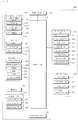
- FIG. 4 is a block diagram of an input voltage stabilization circuit for a rear combination lamp according to an embodiment of the present invention.
- the input voltage stabilization circuit 400 for a rear combination lamp may include a Direct Current to Direct Current (DC-DC) converter 420, an optical output unit 430, a regulator unit 440, a diode AND gate 450, a feedback unit 460, and a converter protector 470.
- DC-DC Direct Current to Direct Current
- a part of the components of the input voltage stabilization circuit 400 may be omitted.
- a component may be added to the input voltage stabilization circuit 400.
- the DC-DC converter 420 may raise or lower a voltage of main power 410.
- the DC-DC converter 420 may be one of a buck-boost converter, a cuk converter, a buck converter, and a boost converter.
- the DC-DC converter 420 may provide an output voltage suitable for driving a plurality of OLEDs.
- the DC-DC converter 420 may adjust the output voltage based on a feedback received from the feedback unit 460. For example, the DC-DC converter 420 may adjust the output voltage so that the feedback received from the feedback unit 460 may be maintained to be a predetermined reference value. For example, the DC-DC converter 420 may adjust the output voltage so that the feedback received from the feedback unit 460 may be maintained to be a predetermined reference range.
- the DC-DC converter 420 may adjust the output voltage based on a feedback received from the converter protector 470.
- An OLED may require a different voltage according to an ambient temperature.
- the OLED may require a voltage ranging from 5V to 20V according to an ambient temperature.
- a relatively high voltage is required at a low temperature, and a relatively low voltage is required at a high temperature.
- the input voltage stabilization circuit 400 enables supply of electrical energy based on the highest of voltages required for the plurality of individual OLEDs.
- the input voltage stabilization circuit 400 enables implementation of a rear combination lamp with OLEDs and stable supply of power to each OLED.
- the optical output unit 430 may include a plurality of OLEDs.
- the rear combination lamp 300 may implement at least one of a brake lamp, a tail lamp, a turn signal lamp, a backup lamp, and a fog lamp, using a plurality of OLEDs.
- the plurality of OLEDs may be divided into a plurality of groups, each including at least one OLED.
- a plurality of OLEDs in a first group may function as a brake lamp under the control of the MCU 500.
- a plurality of OLEDs in a second group may function as a tail lamp under the control of the MCU 500.
- a plurality of OLEDs in a third group may function as a turn signal lamp under the control of the MCU 500.
- a plurality of OLEDs in a fourth group may function as a backup lamp under the control of the MCU 500.
- a plurality of OLEDs in a fifth group may function as a fog lamp under the control of the MCU 500.
- the plurality of OLEDs of a group may function as a plurality of lamps under the control of the MCU 500.
- an OLED may require a different voltage according to an ambient temperature.
- the required voltage may be a voltage for driving the OLED.
- the required voltage may be a voltage for emitting light from the OLED.
- the regulator unit 440 may include a regulator.
- the regulator may be a linear regulator or a switching regulator.
- the regulator unit 440 may include a plurality of regulators mapped to the respective OLEDs.
- the plurality of regulators may be connected individually to the plurality of OLEDs.
- the regulators may stably drive the OLEDs by supplying a predetermined voltage to the OLEDs.
- the regulator may be damaged.
- a threshold for a feedback for operation of the DC-DC converter 420 may be set based on the upper voltage limit for preventing damage to a regulator.
- the diode AND gate 450 may include a diode.
- the diode AND gate 450 may include a plurality of diodes.
- the diode AND gate 450 may include as many diodes as the number of OLEDs included in the optical output unit 430.
- the diodes included in the diode AND gate 450 may be connected to connection nodes between the OLEDs and the regulators. That is, the OLEDs included in the optical output unit 430, the regulators included in the regulator unit 440, and the diodes included in the diode AND gate 450 may be connected to one another, thus forming nodes.
- the plurality of diodes included in the diode AND gate 450 may be connected individually to the plurality of OLEDs included in the optical output unit 430 and the plurality of regulators included in the regulator unit 440.
- the diode AND gate 450 may determine the highest of voltages applied to the plurality of OLEDs.
- the diode AND gate 450 may determine the lowest of voltages applied to the connection nodes between the OLEDs and the regulators based on diode characteristics.
- a voltage of a connection node is calculated by subtracting a voltage decrement incurred by an OLED from an output voltage of the DC-DC converter 420.
- a plurality of connection nodes are formed.
- the lowest of voltages of the plurality of connection nodes may be the highest of voltages applied to the plurality of OLEDs.
- the feedback unit 460 may provide information about the highest of voltages required for the plurality of OLEDs of the optical output unit 430 as a feedback to the DC-DC converter 420.
- the feedback unit 460 may provide information about a voltage value determined by the diode AND gate 450 as a feedback to the DC-DC converter 420.
- the feedback unit 460 may include a voltage division resistor unit and a capacitor unit.
- the voltage division resistor unit may divide a voltage output from the diode AND gate 450 and output a divided voltage as a feedback.
- the voltage division resistor unit may include a plurality of resistors.
- the voltage division resistor unit may divide the voltage output from the diode AND gate 450 into a voltage acceptable for the DC-DC converter 420 by means of the plurality of resistors.
- the capacitor unit may be connected in parallel to the voltage division resistor unit.
- the capacitor unit eliminates ripple or noise.
- the capacitor unit may eliminate the ripple or noise of a feeback.
- the converter protector 470 may protect the DC-DC converter 420, upon occurrence of failure in at least one of the plurality of OLEDs.
- a connection line of the first OLED is open.
- a voltage applied to the first OLED i.e., a required voltage for the first OLED
- the voltage of a node connecting the first OLED to a first regulator becomes 0V.
- the DC-DC converter 420 may continuously raise an output voltage to drive the first OLED, and as a result, may be failed.
- the input voltage stabilization circuit 400 may protect the DC-DC converter 470 even though at least one of the plurality of OLEDs is failed.
- the converter protector 470 may include a first output voltage limiter 480, a second output voltage limiter 490, and a diode OR gate 497.
- the first output voltage limiter 480 may provide information about a limit voltage value for limiting the output voltage of the DC-DC converter 420 as a feedback to the DC-DC converter 420.
- the second output voltage limiter 490 may provide information about a limit voltage value based on temperatures sensed at a plurality of points of a circuit board as a feedback to the DC-DC converter 420.
- the second output voltage limiter 490 may include a plurality of Negative Temperature Coefficient (NTC) thermistors, and a diode AND gate.
- NTC Negative Temperature Coefficient
- the plurality of NTC thermistors may be arranged at a plurality of points of the circuit board.
- the diode AND gate may determine the highest of voltages applied to the individual NTC thermistors.
- the diode OR gate 497 may select the higher between a voltage value output from the first output voltage limiter 480 and a voltage value output from the second output voltage limiter 490.
- the diode OR gate 497 may provide the selected voltage value as a feedback to the DC-DC converter 420.
- the input voltage stabilization circuit 400 may further include a failure sensing unit.
- the failure sensing unit may detect failure of at least one of the plurality of OLEDs.
- the failure sensing unit will be described in greater detail with reference to FIG. 6 .
- the input voltage stabilization circuit 400 may further include the MCU 500.
- the MCU 500 may control an optical output pattern of each of the OLEDs based on a Pulse Width Modulation (PWM) signal.
- PWM Pulse Width Modulation
- the MCU 500 may be implemented using at least one of an ASIC, a DSP, a DSPD, a PLD, an FPGA, a processor, a controller, a micro-controller, a microprocessor, and an electrical unit for executing other functions.
- the input voltage stabilization circuit 400 may further include a main power sensing unit and an emergency power connection unit.
- the main power sensing unit may sense an abnormal state of a main power supply line
- the emergency power connection unit may supply a voltage for providing a PWM signal to the DC-DC converter.
- the main power sensing unit and the emergency power connection unit will be described in greater detail with reference to FIG. 7 .
- FIGS. 5 , 6 , and 7 are exemplary views illustrating input voltage stabilization circuits for a rear combination lamp according to embodiments of the present disclosure.
- the DC-DC converter 420 may raise or lower the voltage of the main power 410 supplied by a vehicle battery.
- the DC-DC converter 420 may adjust an output voltage V out based on a feedback FB received from the feedback unit 460. For example, the DC-DC converter 420 may adjust the output voltage so that the feedback received from the feedback unit 460 may be maintained to be a predetermined reference value.
- the reference value for a feedback may be set based on a limit voltage value for preventing damage to regulators 441 a, 441 b, ..., 441n.
- the DC-DC converter 420 may adjust the output voltage V out based on a feedback FB received from the converter protector 470.
- the optical output unit 430 may include a plurality of OLEDs 431a, 431b, ..., 431n.
- the plurality of OLEDs may require variable voltages according to ambient temperatures.
- first and second OLEDs 431a and 431b may require different voltages depending on positions of the first and second OLEDs 431a and 431b arranged on the circuit board, closeness to the outside of the vehicle, or existence of a nearby heat emission device. If the first OLED 431a requires a higher voltage than the second OLED 431b, the DC-DC converter 420 may have to provide the output voltage V out based on the required voltage of the first OLED 431 a to thereby operate both the first and second OLEDs 431 a and 431b.
- the regulator unit 440 may include the plurality of regulators 441a, 441b,..., 441n.
- the regulator unit 410 may include as many regulators 441a, 441b,..., 441n as the number of the plurality of OLEDs 431a, 431b,..., 431n.
- the plurality of regulators 441a, 441b,..., 441n are connected to the respective OLEDs 431a, 431b,..., 431n and supply a predetermined voltage to each of the OLEDs 431a, 431b,..., 431n. In this case, each of the OLEDs 431a, 431b,..., 431n may be driven stably.
- the plurality of regulators 441a, 441b,..., 441n may be connected individually to the plurality of OLEDs 431a, 431b,..., 431n.
- a plurality of connection nodes A, B,..., N may be formed.
- first OLED 431a and the first regulator 441a may be connected, thereby forming a first connection node A.
- the second OLED 431b and the second regulator 441b may be connected, thereby forming a second connection node B.
- the n th OLED 431n and the n th regulator 441n may be connected, thereby forming an n th connection node N.
- the diode AND gate 450 may include a plurality of diodes 451a, 451b,..., 451n.
- the diode AND gate 450 may include as many diodes as the number of the OLEDs 431a, 431 b,..., 431n or the number of the regulators 441 a, 441 b,..., 441n.
- the plurality of diodes 451a, 451b,..., 451n may be connected to the plurality of OLEDs 431a, 431b,..., 431n and the plurality of the regulators 441a, 441b,..., 441n.
- the first diode 451a may be connected to the first connection node A
- the second diode 451b may be connected to the second connection node B
- the n th diode 451n may be connected to the n th connection node N.
- Cathodes of the plurality of diodes 451a, 451b,..., 451n may be arranged in the direction of the plurality of connection nodes A, B,...,N, and anodes of the plurality of diodes 451 a, 451b,..., 451n may be arranged in the direction of the feedback unit 460.
- the diode AND gate 450 may determine the highest of voltages applied to the plurality of OLEDs 431a, 431b,..., 431n based on diode characteristics.
- the diode AND gate 450 may determine the lowest of voltages applied to the plurality of connection nodes A, B,..., N and output information about the determined voltage to the feedback unit 460.
- a voltage calculated by subtracting a voltage decrement caused by each of the OLEDs 431a, 431b,..., 431n from the output voltage V out of the DC-DC converter 420 is applied to a connection node corresponding to the OLED.
- the lowest of voltages applied to the connection nodes is the highest of voltages applied to the OLEDs.
- the feedback unit 460 may provide information about the highest of voltages required for the plurality of OLEDs 431a, 431b,..., 431n as a feedback to the DC-DC converter 420.
- the feedback unit 460 may provide information about the voltage value determined by the diode AND gate 450 as a feedback to the DC-DC converter 420.
- the diode AND gate 450, the voltage division resistor unit 461, the capacitor unit 462, and a resistor unit 436 may be connected to one another, thereby forming a feedback node a.
- the voltage determined by the diode AND gate 450 may be applied to the feedback node a.
- the voltage division resistor unit 461 may divide the voltage applied to the feedback node a and output a divided voltage to the DC-DC converter 420.
- the capacitor unit 462 may be connected to the voltage division resistor unit 461 in parallel.
- the capacitor unit 462 eliminates ripple or noise.
- the capacitor unit 462 eliminates the ripple or noise of the voltage applied to the feedback node a.
- the converter protector 470 may protect the DC-DC converter 420.
- the converter protector 470 may include the first output voltage limiter 480, the second output voltage limiter 490, and the diode OR gate 497.
- the first output voltage limiter 480 may provide information about a limit voltage value for limiting the output voltage of the DC-DC converter 420 as a feedback to the DC-DC converter 420.
- the first output voltage limiter 480 may include a voltage division resistor unit.
- a first resistor 481 and a second resistor 482 of the voltage division resistor unit are connected to each other, forming a limit voltage node b.
- a voltage divided from the output voltage V out is applied to the limit voltage node b.
- the voltage division resistor unit of the first output voltage limiter 480 may divide a limit voltage value into a voltage acceptable for the DC-DC converter.
- the divided limit voltage value may be output to the diode OR gate 497.
- the second output voltage limiter 490 may provide information about a limit voltage value based on temperatures sensed at a plurality of points of a circuit board as a feedback to the DC-DC converter 420.
- the second output voltage limiter 490 may include a plurality of NTC thermistors 491, and a diode AND gate 492.
- the plurality of NTC thermistors 491 may be arranged at a plurality of points of the circuit board.
- the plurality of NTC thermistors 491 may be arranged at points having low temperatures on the circuit board.
- the plurality of NTC thermistors 491 may be arranged at a point free of a nearby heat emission device or a point near to the outside of the vehicle on the circuit board.
- the diode AND gate 492 may determine the highest of voltages applied to the individual NTC thermistors 491.
- the diode AND gate 492 may determine a point with a lowest temperature from among the points at which the NTC thermistors 491 are arranged.
- the NTC thermistors 491 are characterized in that as temperature increases, resistance decreases.
- the resistance of the NTC thermistors 491 is highest at a point with a lowest temperature among the points at which the NTC thermistors 491 are arranged.
- the diode AND gate 492 may determine the lowest of voltages calculated by subtracting voltages decrements caused by the NTC thermistors 491 from the output voltage V out and output the lowest voltage to the diode OR gate 497.
- the diode OR gate 497 may determine the higher between a voltage value output from the first output voltage limiter 480 and a voltage value output from the second output voltage limiter 490.
- the diode OR gate 497 may provide the determined voltage value as a feedback to the DC-DC converter 420.
- the diode OR gate 497 outputs a voltage from the second output voltage limiter 490 with priority over the first output voltage limiter 480, satisfying the condition that the output voltage V out is less than the limit voltage of the first output voltage limiter 480.
- the input voltage stabilization circuit illustrated in FIG. 6 further includes a failure sensing unit.
- the description of the input voltage stabilization circuit illustrated in FIG. 5 may also be applied to the input voltage stabilization circuit illustrated in FIG. 6 .
- the following description will focus on the failure sensing unit with reference to FIG. 6 .
- a failure sensing unit 600 may sense failure of at least one of the plurality of OLEDs.
- the input voltage stabilization circuit 400 may further include a linear regulator 640.
- the linear regulator 640 may apply a constant voltage to the failure sensing unit 600.
- the failure sensing unit 600 may include an open sensor 610, a latch circuit 620, and a constant current circuit 630.
- the open sensor 610 may include a first transistor Q1, a second transistor Q2, and a delay circuit 611 interposed between the first transistor Q1 and the second transistor Q2.
- the latch circuit 620 may include a third transistor Q3 and a fourth transistor Q4.
- the constant current circuit 630 may include a constant current source 631 and a fifth transistor Q5.
- the second transistor Q2 is turned on, the first transistor Q1 is turned off, the fourth transistor Q4 is turned off, the third transistor Q3 is turned off, and the fifth transistor Q5 is turned on, sequentially.
- current flows by means of the constant current source 631.
- a control signal provider 411 may sense the current flowing by means of the constant current source 631 and thus determine that all of the OLEDs 431a, 431b,...,431n operate normally.
- a voltage output as a feedback becomes 0V or almost 0V.
- the second transistor Q2 is turned off, the first transistor Q1 is turned on, the fourth transistor Q4 is turned on, the third transistor Q3 is turned on, and the fifth transistor Q5 is turned off, sequentially.
- current generated from the constant current source 631 does not flow.
- the control signal provider 411 may fail to sense current flowing by means of the constant current source 631 and thus determine that failure has occurred to at least one of the plurality of OLEDs 431 a, 431b,...,431n.
- the control signal provider 411 may provide failure occurrence information to the controller 170 of the vehicle 100.
- the controller 170 of the vehicle 100 may output failure information about the rear combination lamp 300 through the output unit 140.
- the delay circuit 611 may prevent the first transistor Q1 from operating not by a voltage value output from the feedback unit 460 but by a voltage value provided by the linear regulator 640.
- the latch circuit 620 may keep the fifth transistor Q5 off until before reset.
- the input voltage stabilization circuit illustrated in FIG. 7 further includes an MCU, a main power sensing unit, and an emergency power connection unit, compared to the input voltage stabilization circuit illustrated in FIG. 5 or FIG. 6 .
- the description of the input voltage stabilization circuit illustrated in FIG. 5 or FIG. 6 is applicable to the input voltage stabilization circuit illustrated in FIG. 7 .
- the following description will be given of FIG. 7 , focusing on the MCU, the main power sensing unit, and the emergency power connection unit.
- the MCU 500 may control the optical output pattern of each OLED based on a PWM signal.
- the MCU 500 is shown in FIG. 7 as not connected to other components for the convenience of illustration and convenience, the MCU 500 is electrically connected to other components in real implementation. Specifically, the MCU 500 may be connected to the linear regulator 640 to thereby receive power, and to the optical output unit 430 and the regulator unit 440 to thereby control the plurality of OLEDs 431a, 431b,...,431n.
- the MCU 500 may receive the main power source 410 or power from the control signal provider 411.
- the MCU 500 may receive a control signal SG from the control signal provider 411.
- the input voltage stabilization circuit 400 may further include a main power sensing unit 710 and an emergency power connection unit 720.
- the main power sensing unit 710 may sense an abnormal state of a main power supply line.
- the main power sensing unit 710 may include a first resistor R1, a second resistor R2, a third resistor R3, a first diode D1, a first capacitor C1, and a first transistor Q1.
- the emergency power connection unit 720 may supply a voltage for providing a PWM signal to the DC-DC converter.
- the emergency power connection unit 720 may include a second transistor Q2 and a third transistor Q3.
- the first diode D1 is connected serially to the first capacitor C1.
- the first diode D1 is connected to the main power 410.
- the first transistor Q1 is turned on, the second transistor Q2 is turned off, and the third transistor Q3 is turned off.
- the second resistor R2 is connected in parallel to the first diode D1.
- the second resistor R2 is a discharge resistor. If an external high-voltage surge input is received over a long time, the second resistor R2 prevents the first capacitor C1 from exceeding a withstanding voltage of the first capacitor C1.
- the control signal provider 411 supplies a voltage for providing a PWM signal to the DC-DC converter 420.
- the control signal provider 411 provides a control signal SG to the MCU 500.
- the control signal SG may be a PWM signal.
- the control signal provider 411 may be connected to the DC-DC converter 420 and thus a voltage for providing a PWM signal may be supplied to the DC-DC converter 420.
- FIGS. 8 to 13 are views referred to for describing an operation for controlling a signal of a rear combination lamp according to an embodiment of the present disclosure.
- the MCU 500 may receive a PWM signal from the control signal provider 411.
- the MCU 500 may control the plurality of OLEDs according to the received PWM signal.
- the PWM signal may be configured in various forms.
- the MCU 500 may control a plurality of OLEDs matching a predetermined PWM signal.
- the rear combination lamp 300 may include a left rear combination lamp 300L and a right rear combination lamp 300R.
- the rear combination lamp 300 is described as including six OLEDs in FIGS. 8 to 13 , the number of OLEDs does not limit the scope of the present invention.
- the right rear combination lamp 300R may be controlled in the same manner as the left rear combination lamp 300L.
- the MCU 500 turns on all of the plurality of OLEDs SL1 to SL6.
- the MCU 500 turns off all of the plurality of OLEDs SL1 to SL6.
- the MCU 500 turns on the fifth and sixth OLEDs SL5 and SL6. After a predetermined time elapses, the MCU 500 turns on the third and fourth OLEDs SL3 and SL4. Then after a predetermined time elapses, the MCU 500 turns on the first and second OLEDs SL1 and SL2.
- the MCU 500 turns off the fifth and sixth OLEDs SL5 and SL6. After a predetermined time elapses, the MCU 500 turns off the third and fourth OLEDs SL3 and SL4. Then after a predetermined time elapses, the MCU 500 turns off the first and second OLEDs SL1 and SL2.
- the MCU 500 turns on the sixth OLED SL6. Then, the MCU 500 turns on the fourth OLED SL4. Then, the MCU 500 turns on the second OLED SL2.
- an operation of a turn signal lamp may be performed by sequentially turning on a plurality of OLEDs.
- the MCU 500 turns on the sixth OLED SL6. Then, the MCU 500 turns on the fourth OLED SL4. Then, the MCU 500 turns on the second OLED SL2.
- an operation of a turn signal lamp may be performed by sequentially turning on a plurality of OLEDs.
- a signal can be effectively transmitted using an OLED in a rear combination lamp, without dazzling a driver of another vehicle.
- various signals may be transmitted using a plurality of OLEDs.
- OLEDs can be driven stably despite a change of an ambient temperature.
- a circuit device can be minimized, a circuit board space can be secured, and load on an MCU can be minimized.
- the present invention may be implemented as code that can be written on a computer-readable recording medium and thus read by a computer system.
- the computer-readable recording medium may be any type of recording device in which data is stored in a computer-readable manner. Examples of the computer-readable recording medium include a Hard Disk Drive (HDD), a Solid State Disk (SSD), a Silicon Disk Drive (SDD), a Read Only Memory (ROM), a Random Access Memory (RAM), a Compact Disk ROM (CD-ROM), a magnetic tape, a floppy disc, an optical data storage, and a carrier wave (e.g., data transmission over the Internet).
- the computer may include a processor a controller.
Landscapes
- Engineering & Computer Science (AREA)
- Mechanical Engineering (AREA)
- Physics & Mathematics (AREA)
- Microelectronics & Electronic Packaging (AREA)
- Optics & Photonics (AREA)
- General Engineering & Computer Science (AREA)
- Lighting Device Outwards From Vehicle And Optical Signal (AREA)
Applications Claiming Priority (1)
| Application Number | Priority Date | Filing Date | Title |
|---|---|---|---|
| KR1020160073815A KR101822889B1 (ko) | 2016-06-14 | 2016-06-14 | 리어 콤비네이션 램프의 입력 전압 안정화 회로, 리어 콤비네이션 램프 및 차량 |
Publications (2)
| Publication Number | Publication Date |
|---|---|
| EP3258745A1 true EP3258745A1 (fr) | 2017-12-20 |
| EP3258745B1 EP3258745B1 (fr) | 2020-04-29 |
Family
ID=58530386
Family Applications (1)
| Application Number | Title | Priority Date | Filing Date |
|---|---|---|---|
| EP17164959.3A Active EP3258745B1 (fr) | 2016-06-14 | 2017-04-05 | Circuit de stabilisation de tension d'entrée de lampe de combinaison arrière, lampe de combinaison arrière et véhicule |
Country Status (4)
| Country | Link |
|---|---|
| US (1) | US10342095B2 (fr) |
| EP (1) | EP3258745B1 (fr) |
| KR (1) | KR101822889B1 (fr) |
| CN (1) | CN107499226B (fr) |
Cited By (3)
| Publication number | Priority date | Publication date | Assignee | Title |
|---|---|---|---|---|
| CN110267398A (zh) * | 2019-06-17 | 2019-09-20 | 上汽大众汽车有限公司 | 制动灯电路、制动灯系统及制动灯动态熄灭的方法 |
| FR3105704A1 (fr) * | 2019-12-19 | 2021-06-25 | Valeo Vision | Systeme de pilotage de l’alimentation electrique de sources lumineuses |
| EP3344012B1 (fr) * | 2016-12-29 | 2023-07-05 | MARELLI AUTOMOTIVE LIGHTING ITALY S.p.A. | Circuit d'attaque de sources lumineuses, en particulier pour un phare de véhicule |
Families Citing this family (4)
| Publication number | Priority date | Publication date | Assignee | Title |
|---|---|---|---|---|
| US10714633B2 (en) | 2015-12-15 | 2020-07-14 | Semiconductor Energy Laboratory Co., Ltd. | Semiconductor device and display device |
| EP3691414B1 (fr) | 2019-01-31 | 2023-11-01 | Valeo Iluminacion | Dispositif et procédé d'éclairage automobile |
| EP4122025A4 (fr) * | 2020-03-18 | 2024-04-10 | Saint-Gobain Glass France | Système d'affichage optimisé pour véhicule |
| CN113859395B (zh) * | 2021-12-02 | 2022-04-29 | 宁波明讯实业有限公司 | 一种新能源汽车组合尾灯支座焊接总成 |
Citations (5)
| Publication number | Priority date | Publication date | Assignee | Title |
|---|---|---|---|---|
| DE20004810U1 (de) * | 2000-03-16 | 2000-12-14 | Engel, Manfred, 24558 Henstedt-Ulzburg | Verkehrswarneinrichtung nach Unfällen bei schlechter Sicht |
| US7573210B2 (en) * | 2004-10-12 | 2009-08-11 | Koninklijke Philips Electronics N.V. | Method and system for feedback and control of a luminaire |
| US20100013395A1 (en) * | 2008-07-15 | 2010-01-21 | Intersil Americas, Inc | Dynamic headroom control for lcd driver |
| US20110062872A1 (en) * | 2009-09-11 | 2011-03-17 | Xuecheng Jin | Adaptive Switch Mode LED Driver |
| US20120314463A1 (en) * | 2011-06-09 | 2012-12-13 | Osram Sylvania Inc. | Power supply with restart circuit |
Family Cites Families (18)
| Publication number | Priority date | Publication date | Assignee | Title |
|---|---|---|---|---|
| JP4148746B2 (ja) * | 2002-10-08 | 2008-09-10 | 株式会社小糸製作所 | 点灯回路 |
| JP4148908B2 (ja) * | 2004-02-16 | 2008-09-10 | 株式会社小糸製作所 | 車両用灯具 |
| US20070273681A1 (en) * | 2006-05-24 | 2007-11-29 | Mayell Robert J | Method and apparatus to power light emitting diode arrays |
| JP2009184592A (ja) * | 2008-02-08 | 2009-08-20 | Koito Mfg Co Ltd | 車両用灯具の点灯制御装置 |
| US8004207B2 (en) * | 2008-12-03 | 2011-08-23 | Freescale Semiconductor, Inc. | LED driver with precharge and track/hold |
| FR2960119B1 (fr) * | 2010-05-12 | 2012-08-03 | Valeo Vision | Module de pilotage d'alimentation d'ensembles de led |
| KR20130012670A (ko) | 2011-07-26 | 2013-02-05 | 삼성디스플레이 주식회사 | 백라이트 유닛 및 그것의 전류 제어 방법 |
| JP5526095B2 (ja) * | 2011-09-20 | 2014-06-18 | 日立アプライアンス株式会社 | Led点灯装置 |
| JP2014019171A (ja) * | 2012-07-12 | 2014-02-03 | Yamaha Motor Co Ltd | 方向指示器及びそれを備えた鞍乗型車両用方向指示装置 |
| KR20140079932A (ko) | 2012-12-20 | 2014-06-30 | 에스엘 주식회사 | 차량용 램프 |
| US8928256B2 (en) * | 2013-04-26 | 2015-01-06 | Phoseon Technology, Inc. | Method and system for light array thermal slope detection |
| US9504103B2 (en) * | 2013-10-21 | 2016-11-22 | Osram Sylvania Inc. | Driving a multi-color luminaire |
| KR20150121868A (ko) | 2014-04-22 | 2015-10-30 | 주식회사 제논엘이디 | 엘이디를 이용한 등기구 전원 관리 시스템 |
| US9618162B2 (en) * | 2014-04-25 | 2017-04-11 | Cree, Inc. | LED lamp |
| KR101687358B1 (ko) | 2014-05-21 | 2016-12-16 | 이민진 | 엘이디 컨버터 보호회로 |
| JP6440061B2 (ja) * | 2014-07-15 | 2018-12-19 | パナソニックIpマネジメント株式会社 | 点灯装置、照明装置及び車両用前照灯装置 |
| CN204472673U (zh) * | 2015-01-08 | 2015-07-15 | 台州市伊悦尼塑模有限公司 | Led汽车转向灯 |
| JP6470083B2 (ja) * | 2015-03-20 | 2019-02-13 | ローム株式会社 | スイッチ駆動装置、発光装置、車両 |
-
2016
- 2016-06-14 KR KR1020160073815A patent/KR101822889B1/ko active IP Right Grant
-
2017
- 2017-03-15 CN CN201710152641.2A patent/CN107499226B/zh active Active
- 2017-04-05 EP EP17164959.3A patent/EP3258745B1/fr active Active
- 2017-06-14 US US15/622,942 patent/US10342095B2/en active Active
Patent Citations (5)
| Publication number | Priority date | Publication date | Assignee | Title |
|---|---|---|---|---|
| DE20004810U1 (de) * | 2000-03-16 | 2000-12-14 | Engel, Manfred, 24558 Henstedt-Ulzburg | Verkehrswarneinrichtung nach Unfällen bei schlechter Sicht |
| US7573210B2 (en) * | 2004-10-12 | 2009-08-11 | Koninklijke Philips Electronics N.V. | Method and system for feedback and control of a luminaire |
| US20100013395A1 (en) * | 2008-07-15 | 2010-01-21 | Intersil Americas, Inc | Dynamic headroom control for lcd driver |
| US20110062872A1 (en) * | 2009-09-11 | 2011-03-17 | Xuecheng Jin | Adaptive Switch Mode LED Driver |
| US20120314463A1 (en) * | 2011-06-09 | 2012-12-13 | Osram Sylvania Inc. | Power supply with restart circuit |
Cited By (3)
| Publication number | Priority date | Publication date | Assignee | Title |
|---|---|---|---|---|
| EP3344012B1 (fr) * | 2016-12-29 | 2023-07-05 | MARELLI AUTOMOTIVE LIGHTING ITALY S.p.A. | Circuit d'attaque de sources lumineuses, en particulier pour un phare de véhicule |
| CN110267398A (zh) * | 2019-06-17 | 2019-09-20 | 上汽大众汽车有限公司 | 制动灯电路、制动灯系统及制动灯动态熄灭的方法 |
| FR3105704A1 (fr) * | 2019-12-19 | 2021-06-25 | Valeo Vision | Systeme de pilotage de l’alimentation electrique de sources lumineuses |
Also Published As
| Publication number | Publication date |
|---|---|
| CN107499226B (zh) | 2020-06-09 |
| US10342095B2 (en) | 2019-07-02 |
| KR101822889B1 (ko) | 2018-03-08 |
| EP3258745B1 (fr) | 2020-04-29 |
| US20180014376A1 (en) | 2018-01-11 |
| CN107499226A (zh) | 2017-12-22 |
| KR20170140978A (ko) | 2017-12-22 |
Similar Documents
| Publication | Publication Date | Title |
|---|---|---|
| EP3258745B1 (fr) | Circuit de stabilisation de tension d'entrée de lampe de combinaison arrière, lampe de combinaison arrière et véhicule | |
| US10496892B2 (en) | Apparatus for providing around view image, and vehicle | |
| US9969320B2 (en) | Lamp and autonomous vehicle | |
| EP3190005B1 (fr) | Phare de véhicule et véhicule le comprenant | |
| CN109507994B (zh) | 安装在车辆上的车辆控制装置以及控制该车辆的方法 | |
| US10528053B2 (en) | Vehicle control device mounted on vehicle and method for controlling the vehicle | |
| EP3428027B1 (fr) | Système d'entraînement pour véhicule | |
| US10691132B2 (en) | Vehicle control device mounted on vehicle and method for controlling the vehicle | |
| US20190088125A1 (en) | Vehicle having a communication device for conducting vehicle to everything (v2x) communications | |
| US10942523B2 (en) | Autonomous vehicle and method of controlling the same | |
| US11305654B2 (en) | Apparatus for controlling energy consumption and method thereof | |
| US10414328B2 (en) | Lamp for vehicle and vehicle comprising the same | |
| US20190111917A1 (en) | Autonomous vehicle and method of controlling the same | |
| US11046291B2 (en) | Vehicle driver assistance apparatus and vehicle | |
| US20190375397A1 (en) | Vehicle control device included in vehicle and control method for vehicle | |
| US10768618B2 (en) | Vehicle driving control apparatus and vehicle driving method | |
| KR101858700B1 (ko) | 리어 콤비네이션 램프의 구동 회로, 리어 콤비네이션 램프 및 차량 |
Legal Events
| Date | Code | Title | Description |
|---|---|---|---|
| PUAI | Public reference made under article 153(3) epc to a published international application that has entered the european phase |
Free format text: ORIGINAL CODE: 0009012 |
|
| STAA | Information on the status of an ep patent application or granted ep patent |
Free format text: STATUS: THE APPLICATION HAS BEEN PUBLISHED |
|
| AK | Designated contracting states |
Kind code of ref document: A1 Designated state(s): AL AT BE BG CH CY CZ DE DK EE ES FI FR GB GR HR HU IE IS IT LI LT LU LV MC MK MT NL NO PL PT RO RS SE SI SK SM TR |
|
| AX | Request for extension of the european patent |
Extension state: BA ME |
|
| STAA | Information on the status of an ep patent application or granted ep patent |
Free format text: STATUS: REQUEST FOR EXAMINATION WAS MADE |
|
| 17P | Request for examination filed |
Effective date: 20180522 |
|
| RBV | Designated contracting states (corrected) |
Designated state(s): AL AT BE BG CH CY CZ DE DK EE ES FI FR GB GR HR HU IE IS IT LI LT LU LV MC MK MT NL NO PL PT RO RS SE SI SK SM TR |
|
| STAA | Information on the status of an ep patent application or granted ep patent |
Free format text: STATUS: EXAMINATION IS IN PROGRESS |
|
| 17Q | First examination report despatched |
Effective date: 20190618 |
|
| GRAP | Despatch of communication of intention to grant a patent |
Free format text: ORIGINAL CODE: EPIDOSNIGR1 |
|
| STAA | Information on the status of an ep patent application or granted ep patent |
Free format text: STATUS: GRANT OF PATENT IS INTENDED |
|
| INTG | Intention to grant announced |
Effective date: 20191209 |
|
| GRAS | Grant fee paid |
Free format text: ORIGINAL CODE: EPIDOSNIGR3 |
|
| GRAA | (expected) grant |
Free format text: ORIGINAL CODE: 0009210 |
|
| STAA | Information on the status of an ep patent application or granted ep patent |
Free format text: STATUS: THE PATENT HAS BEEN GRANTED |
|
| AK | Designated contracting states |
Kind code of ref document: B1 Designated state(s): AL AT BE BG CH CY CZ DE DK EE ES FI FR GB GR HR HU IE IS IT LI LT LU LV MC MK MT NL NO PL PT RO RS SE SI SK SM TR |
|
| REG | Reference to a national code |
Ref country code: GB Ref legal event code: FG4D |
|
| REG | Reference to a national code |
Ref country code: CH Ref legal event code: EP |
|
| REG | Reference to a national code |
Ref country code: AT Ref legal event code: REF Ref document number: 1265292 Country of ref document: AT Kind code of ref document: T Effective date: 20200515 |
|
| REG | Reference to a national code |
Ref country code: DE Ref legal event code: R096 Ref document number: 602017015488 Country of ref document: DE |
|
| REG | Reference to a national code |
Ref country code: IE Ref legal event code: FG4D |
|
| RAP2 | Party data changed (patent owner data changed or rights of a patent transferred) |
Owner name: ZKW GROUP GMBH |
|
| REG | Reference to a national code |
Ref country code: DE Ref legal event code: R082 Ref document number: 602017015488 Country of ref document: DE Representative=s name: K & H BONAPAT PATENTANWAELTE KOCH VON BEHREN &, DE Ref country code: DE Ref legal event code: R081 Ref document number: 602017015488 Country of ref document: DE Owner name: ZKW GROUP GMBH, AT Free format text: FORMER OWNER: LG ELECTRONICS INC., SEOUL, KR |
|
| REG | Reference to a national code |
Ref country code: NL Ref legal event code: MP Effective date: 20200429 |
|
| REG | Reference to a national code |
Ref country code: LT Ref legal event code: MG4D |
|
| PG25 | Lapsed in a contracting state [announced via postgrant information from national office to epo] |
Ref country code: SE Free format text: LAPSE BECAUSE OF FAILURE TO SUBMIT A TRANSLATION OF THE DESCRIPTION OR TO PAY THE FEE WITHIN THE PRESCRIBED TIME-LIMIT Effective date: 20200429 Ref country code: FI Free format text: LAPSE BECAUSE OF FAILURE TO SUBMIT A TRANSLATION OF THE DESCRIPTION OR TO PAY THE FEE WITHIN THE PRESCRIBED TIME-LIMIT Effective date: 20200429 Ref country code: PT Free format text: LAPSE BECAUSE OF FAILURE TO SUBMIT A TRANSLATION OF THE DESCRIPTION OR TO PAY THE FEE WITHIN THE PRESCRIBED TIME-LIMIT Effective date: 20200831 Ref country code: NO Free format text: LAPSE BECAUSE OF FAILURE TO SUBMIT A TRANSLATION OF THE DESCRIPTION OR TO PAY THE FEE WITHIN THE PRESCRIBED TIME-LIMIT Effective date: 20200729 Ref country code: IS Free format text: LAPSE BECAUSE OF FAILURE TO SUBMIT A TRANSLATION OF THE DESCRIPTION OR TO PAY THE FEE WITHIN THE PRESCRIBED TIME-LIMIT Effective date: 20200829 Ref country code: GR Free format text: LAPSE BECAUSE OF FAILURE TO SUBMIT A TRANSLATION OF THE DESCRIPTION OR TO PAY THE FEE WITHIN THE PRESCRIBED TIME-LIMIT Effective date: 20200730 Ref country code: LT Free format text: LAPSE BECAUSE OF FAILURE TO SUBMIT A TRANSLATION OF THE DESCRIPTION OR TO PAY THE FEE WITHIN THE PRESCRIBED TIME-LIMIT Effective date: 20200429 |
|
| REG | Reference to a national code |
Ref country code: AT Ref legal event code: MK05 Ref document number: 1265292 Country of ref document: AT Kind code of ref document: T Effective date: 20200429 |
|
| PG25 | Lapsed in a contracting state [announced via postgrant information from national office to epo] |
Ref country code: LV Free format text: LAPSE BECAUSE OF FAILURE TO SUBMIT A TRANSLATION OF THE DESCRIPTION OR TO PAY THE FEE WITHIN THE PRESCRIBED TIME-LIMIT Effective date: 20200429 Ref country code: HR Free format text: LAPSE BECAUSE OF FAILURE TO SUBMIT A TRANSLATION OF THE DESCRIPTION OR TO PAY THE FEE WITHIN THE PRESCRIBED TIME-LIMIT Effective date: 20200429 Ref country code: RS Free format text: LAPSE BECAUSE OF FAILURE TO SUBMIT A TRANSLATION OF THE DESCRIPTION OR TO PAY THE FEE WITHIN THE PRESCRIBED TIME-LIMIT Effective date: 20200429 Ref country code: BG Free format text: LAPSE BECAUSE OF FAILURE TO SUBMIT A TRANSLATION OF THE DESCRIPTION OR TO PAY THE FEE WITHIN THE PRESCRIBED TIME-LIMIT Effective date: 20200729 |
|
| PG25 | Lapsed in a contracting state [announced via postgrant information from national office to epo] |
Ref country code: NL Free format text: LAPSE BECAUSE OF FAILURE TO SUBMIT A TRANSLATION OF THE DESCRIPTION OR TO PAY THE FEE WITHIN THE PRESCRIBED TIME-LIMIT Effective date: 20200429 Ref country code: AL Free format text: LAPSE BECAUSE OF FAILURE TO SUBMIT A TRANSLATION OF THE DESCRIPTION OR TO PAY THE FEE WITHIN THE PRESCRIBED TIME-LIMIT Effective date: 20200429 |
|
| PG25 | Lapsed in a contracting state [announced via postgrant information from national office to epo] |
Ref country code: IT Free format text: LAPSE BECAUSE OF FAILURE TO SUBMIT A TRANSLATION OF THE DESCRIPTION OR TO PAY THE FEE WITHIN THE PRESCRIBED TIME-LIMIT Effective date: 20200429 Ref country code: RO Free format text: LAPSE BECAUSE OF FAILURE TO SUBMIT A TRANSLATION OF THE DESCRIPTION OR TO PAY THE FEE WITHIN THE PRESCRIBED TIME-LIMIT Effective date: 20200429 Ref country code: SM Free format text: LAPSE BECAUSE OF FAILURE TO SUBMIT A TRANSLATION OF THE DESCRIPTION OR TO PAY THE FEE WITHIN THE PRESCRIBED TIME-LIMIT Effective date: 20200429 Ref country code: DK Free format text: LAPSE BECAUSE OF FAILURE TO SUBMIT A TRANSLATION OF THE DESCRIPTION OR TO PAY THE FEE WITHIN THE PRESCRIBED TIME-LIMIT Effective date: 20200429 Ref country code: EE Free format text: LAPSE BECAUSE OF FAILURE TO SUBMIT A TRANSLATION OF THE DESCRIPTION OR TO PAY THE FEE WITHIN THE PRESCRIBED TIME-LIMIT Effective date: 20200429 Ref country code: AT Free format text: LAPSE BECAUSE OF FAILURE TO SUBMIT A TRANSLATION OF THE DESCRIPTION OR TO PAY THE FEE WITHIN THE PRESCRIBED TIME-LIMIT Effective date: 20200429 Ref country code: ES Free format text: LAPSE BECAUSE OF FAILURE TO SUBMIT A TRANSLATION OF THE DESCRIPTION OR TO PAY THE FEE WITHIN THE PRESCRIBED TIME-LIMIT Effective date: 20200429 Ref country code: CZ Free format text: LAPSE BECAUSE OF FAILURE TO SUBMIT A TRANSLATION OF THE DESCRIPTION OR TO PAY THE FEE WITHIN THE PRESCRIBED TIME-LIMIT Effective date: 20200429 |
|
| REG | Reference to a national code |
Ref country code: DE Ref legal event code: R097 Ref document number: 602017015488 Country of ref document: DE |
|
| PG25 | Lapsed in a contracting state [announced via postgrant information from national office to epo] |
Ref country code: SK Free format text: LAPSE BECAUSE OF FAILURE TO SUBMIT A TRANSLATION OF THE DESCRIPTION OR TO PAY THE FEE WITHIN THE PRESCRIBED TIME-LIMIT Effective date: 20200429 Ref country code: PL Free format text: LAPSE BECAUSE OF FAILURE TO SUBMIT A TRANSLATION OF THE DESCRIPTION OR TO PAY THE FEE WITHIN THE PRESCRIBED TIME-LIMIT Effective date: 20200429 |
|
| PLBE | No opposition filed within time limit |
Free format text: ORIGINAL CODE: 0009261 |
|
| STAA | Information on the status of an ep patent application or granted ep patent |
Free format text: STATUS: NO OPPOSITION FILED WITHIN TIME LIMIT |
|
| 26N | No opposition filed |
Effective date: 20210201 |
|
| PG25 | Lapsed in a contracting state [announced via postgrant information from national office to epo] |
Ref country code: SI Free format text: LAPSE BECAUSE OF FAILURE TO SUBMIT A TRANSLATION OF THE DESCRIPTION OR TO PAY THE FEE WITHIN THE PRESCRIBED TIME-LIMIT Effective date: 20200429 |
|
| REG | Reference to a national code |
Ref country code: DE Ref legal event code: R079 Ref document number: 602017015488 Country of ref document: DE Free format text: PREVIOUS MAIN CLASS: H05B0033080000 Ipc: H05B0044000000 |
|
| PG25 | Lapsed in a contracting state [announced via postgrant information from national office to epo] |
Ref country code: MC Free format text: LAPSE BECAUSE OF FAILURE TO SUBMIT A TRANSLATION OF THE DESCRIPTION OR TO PAY THE FEE WITHIN THE PRESCRIBED TIME-LIMIT Effective date: 20200429 |
|
| GBPC | Gb: european patent ceased through non-payment of renewal fee |
Effective date: 20210405 |
|
| PG25 | Lapsed in a contracting state [announced via postgrant information from national office to epo] |
Ref country code: LU Free format text: LAPSE BECAUSE OF NON-PAYMENT OF DUE FEES Effective date: 20210405 |
|
| REG | Reference to a national code |
Ref country code: BE Ref legal event code: MM Effective date: 20210430 |
|
| PG25 | Lapsed in a contracting state [announced via postgrant information from national office to epo] |
Ref country code: GB Free format text: LAPSE BECAUSE OF NON-PAYMENT OF DUE FEES Effective date: 20210405 Ref country code: LI Free format text: LAPSE BECAUSE OF NON-PAYMENT OF DUE FEES Effective date: 20210430 Ref country code: CH Free format text: LAPSE BECAUSE OF NON-PAYMENT OF DUE FEES Effective date: 20210430 |
|
| PG25 | Lapsed in a contracting state [announced via postgrant information from national office to epo] |
Ref country code: IE Free format text: LAPSE BECAUSE OF NON-PAYMENT OF DUE FEES Effective date: 20210405 |
|
| PG25 | Lapsed in a contracting state [announced via postgrant information from national office to epo] |
Ref country code: BE Free format text: LAPSE BECAUSE OF NON-PAYMENT OF DUE FEES Effective date: 20210430 |
|
| PG25 | Lapsed in a contracting state [announced via postgrant information from national office to epo] |
Ref country code: HU Free format text: LAPSE BECAUSE OF FAILURE TO SUBMIT A TRANSLATION OF THE DESCRIPTION OR TO PAY THE FEE WITHIN THE PRESCRIBED TIME-LIMIT; INVALID AB INITIO Effective date: 20170405 |
|
| PG25 | Lapsed in a contracting state [announced via postgrant information from national office to epo] |
Ref country code: CY Free format text: LAPSE BECAUSE OF FAILURE TO SUBMIT A TRANSLATION OF THE DESCRIPTION OR TO PAY THE FEE WITHIN THE PRESCRIBED TIME-LIMIT Effective date: 20200429 |
|
| P01 | Opt-out of the competence of the unified patent court (upc) registered |
Effective date: 20230528 |
|
| PG25 | Lapsed in a contracting state [announced via postgrant information from national office to epo] |
Ref country code: MK Free format text: LAPSE BECAUSE OF FAILURE TO SUBMIT A TRANSLATION OF THE DESCRIPTION OR TO PAY THE FEE WITHIN THE PRESCRIBED TIME-LIMIT Effective date: 20200429 |
|
| PG25 | Lapsed in a contracting state [announced via postgrant information from national office to epo] |
Ref country code: TR Free format text: LAPSE BECAUSE OF FAILURE TO SUBMIT A TRANSLATION OF THE DESCRIPTION OR TO PAY THE FEE WITHIN THE PRESCRIBED TIME-LIMIT Effective date: 20200429 |
|
| PGFP | Annual fee paid to national office [announced via postgrant information from national office to epo] |
Ref country code: DE Payment date: 20240418 Year of fee payment: 8 |
|
| PGFP | Annual fee paid to national office [announced via postgrant information from national office to epo] |
Ref country code: FR Payment date: 20240425 Year of fee payment: 8 |