EP3258488A1 - Halbleiterbauelement mit geschützten seitenwänden - Google Patents
Halbleiterbauelement mit geschützten seitenwänden Download PDFInfo
- Publication number
- EP3258488A1 EP3258488A1 EP17165113.6A EP17165113A EP3258488A1 EP 3258488 A1 EP3258488 A1 EP 3258488A1 EP 17165113 A EP17165113 A EP 17165113A EP 3258488 A1 EP3258488 A1 EP 3258488A1
- Authority
- EP
- European Patent Office
- Prior art keywords
- semiconductor wafer
- wafer
- semiconductor
- carrier
- backside
- Prior art date
- Legal status (The legal status is an assumption and is not a legal conclusion. Google has not performed a legal analysis and makes no representation as to the accuracy of the status listed.)
- Withdrawn
Links
Images


Classifications
-
- H—ELECTRICITY
- H10—SEMICONDUCTOR DEVICES; ELECTRIC SOLID-STATE DEVICES NOT OTHERWISE PROVIDED FOR
- H10W—GENERIC PACKAGES, INTERCONNECTIONS, CONNECTORS OR OTHER CONSTRUCTIONAL DETAILS OF DEVICES COVERED BY CLASS H10
- H10W42/00—Arrangements for protection of devices
- H10W42/121—Arrangements for protection of devices protecting against mechanical damage
-
- H—ELECTRICITY
- H10—SEMICONDUCTOR DEVICES; ELECTRIC SOLID-STATE DEVICES NOT OTHERWISE PROVIDED FOR
- H10P—GENERIC PROCESSES OR APPARATUS FOR THE MANUFACTURE OR TREATMENT OF DEVICES COVERED BY CLASS H10
- H10P54/00—Cutting or separating of wafers, substrates or parts of devices
-
- H—ELECTRICITY
- H10—SEMICONDUCTOR DEVICES; ELECTRIC SOLID-STATE DEVICES NOT OTHERWISE PROVIDED FOR
- H10P—GENERIC PROCESSES OR APPARATUS FOR THE MANUFACTURE OR TREATMENT OF DEVICES COVERED BY CLASS H10
- H10P72/00—Handling or holding of wafers, substrates or devices during manufacture or treatment thereof
- H10P72/70—Handling or holding of wafers, substrates or devices during manufacture or treatment thereof for supporting or gripping
- H10P72/74—Handling or holding of wafers, substrates or devices during manufacture or treatment thereof for supporting or gripping using temporarily an auxiliary support
-
- H—ELECTRICITY
- H10—SEMICONDUCTOR DEVICES; ELECTRIC SOLID-STATE DEVICES NOT OTHERWISE PROVIDED FOR
- H10W—GENERIC PACKAGES, INTERCONNECTIONS, CONNECTORS OR OTHER CONSTRUCTIONAL DETAILS OF DEVICES COVERED BY CLASS H10
- H10W46/00—Marks applied to devices, e.g. for alignment or identification
-
- H—ELECTRICITY
- H10—SEMICONDUCTOR DEVICES; ELECTRIC SOLID-STATE DEVICES NOT OTHERWISE PROVIDED FOR
- H10W—GENERIC PACKAGES, INTERCONNECTIONS, CONNECTORS OR OTHER CONSTRUCTIONAL DETAILS OF DEVICES COVERED BY CLASS H10
- H10W72/00—Interconnections or connectors in packages
- H10W72/20—Bump connectors, e.g. solder bumps or copper pillars; Dummy bumps; Thermal bumps
-
- H—ELECTRICITY
- H10—SEMICONDUCTOR DEVICES; ELECTRIC SOLID-STATE DEVICES NOT OTHERWISE PROVIDED FOR
- H10W—GENERIC PACKAGES, INTERCONNECTIONS, CONNECTORS OR OTHER CONSTRUCTIONAL DETAILS OF DEVICES COVERED BY CLASS H10
- H10W74/00—Encapsulations, e.g. protective coatings
- H10W74/01—Manufacture or treatment
- H10W74/014—Manufacture or treatment using batch processing
-
- H—ELECTRICITY
- H10—SEMICONDUCTOR DEVICES; ELECTRIC SOLID-STATE DEVICES NOT OTHERWISE PROVIDED FOR
- H10W—GENERIC PACKAGES, INTERCONNECTIONS, CONNECTORS OR OTHER CONSTRUCTIONAL DETAILS OF DEVICES COVERED BY CLASS H10
- H10W74/00—Encapsulations, e.g. protective coatings
- H10W74/10—Encapsulations, e.g. protective coatings characterised by their shape or disposition
- H10W74/111—Encapsulations, e.g. protective coatings characterised by their shape or disposition the semiconductor body being completely enclosed
- H10W74/129—Encapsulations, e.g. protective coatings characterised by their shape or disposition the semiconductor body being completely enclosed forming a chip-scale package [CSP]
-
- H—ELECTRICITY
- H10—SEMICONDUCTOR DEVICES; ELECTRIC SOLID-STATE DEVICES NOT OTHERWISE PROVIDED FOR
- H10W—GENERIC PACKAGES, INTERCONNECTIONS, CONNECTORS OR OTHER CONSTRUCTIONAL DETAILS OF DEVICES COVERED BY CLASS H10
- H10W74/00—Encapsulations, e.g. protective coatings
- H10W74/10—Encapsulations, e.g. protective coatings characterised by their shape or disposition
- H10W74/131—Encapsulations, e.g. protective coatings characterised by their shape or disposition the semiconductor body being only partially enclosed
- H10W74/141—Encapsulations, e.g. protective coatings characterised by their shape or disposition the semiconductor body being only partially enclosed the encapsulations being on at least the sidewalls of the semiconductor body
-
- H—ELECTRICITY
- H10—SEMICONDUCTOR DEVICES; ELECTRIC SOLID-STATE DEVICES NOT OTHERWISE PROVIDED FOR
- H10W—GENERIC PACKAGES, INTERCONNECTIONS, CONNECTORS OR OTHER CONSTRUCTIONAL DETAILS OF DEVICES COVERED BY CLASS H10
- H10W46/00—Marks applied to devices, e.g. for alignment or identification
- H10W46/501—Marks applied to devices, e.g. for alignment or identification for use before dicing
- H10W46/503—Located in scribe lines
-
- H—ELECTRICITY
- H10—SEMICONDUCTOR DEVICES; ELECTRIC SOLID-STATE DEVICES NOT OTHERWISE PROVIDED FOR
- H10W—GENERIC PACKAGES, INTERCONNECTIONS, CONNECTORS OR OTHER CONSTRUCTIONAL DETAILS OF DEVICES COVERED BY CLASS H10
- H10W74/00—Encapsulations, e.g. protective coatings
- H10W74/01—Manufacture or treatment
- H10W74/019—Manufacture or treatment using temporary auxiliary substrates
Definitions
- An electronic component such as an integrated circuit typically uses a small piece of silicon wafer. However, its final size becomes much bigger after packaging and adding contact pins. Solder balls or pads are increasingly being used on the bottom of integrated circuits or even discrete components to replace conventional metal pins and wire bonds.
- a semiconductor component e.g., an integrated circuit
- a semiconductor component mostly needs to be packaged to provide sidewall protection and preventing cracks.
- Figure 1 shows a section of a system 100 in which a device 102 is shown as being soldered to solder pads on a printed circuit board (PCB). As depicted, due to a small size, there is a likelihood that solder material 104 may touch sidewalls of the device 102.
- PCB printed circuit board
- a method of protecting sidewalls a plurality of semiconductor devices includes (a) fabricating the plurality of semiconductor devices on a semiconductor wafer, (b) forming a plurality of contact pads on each of the plurality of semiconductor devices, (c) forming an isolation layer to cover a surface of the semiconductor wafer such that the plurality of contact pads are covered by the isolation layer, (d) placing the semiconductor wafer on a carrier such that a backside of the semiconductor wafer is facing up and a front side is facing down and non-permanently affixed to the surface of the carrier, (e) etching to form a trench grid network on the backside of the semiconductor wafer.
- the trench grid network demarcate physical boundaries of each of the plurality of semiconductor devices.
- the method further includes (f) depositing a protective layer on the backside and (g) etching to remove the protective layer from horizontal surfaces and to singulate each of the plurality of semiconductor devices from the semiconductor wafer.
- the carrier includes a sticky foil. In other embodiments, he carrier includes a buffer wafer. In some embodiments, the forming of the isolation layer includes etching the isolation layer to expose a surface of the plurality of contact pads.
- the protective layer is deposited in gaseous form.
- the protective layer is made of Parylene or similar type of material as conformal coating.
- steps (a) to (g) are performed in sequentially in the listed order.
- a semiconductor device manufactured using an operation on a backside of a wafer includes (a) fabricating the plurality of semiconductor devices on a semiconductor wafer, (b) forming a plurality of contact pads on each of the plurality of semiconductor devices, (c) forming an isolation layer to cover a surface of the semiconductor wafer such that the plurality of contact pads are covered by the isolation layer, (d) placing the semiconductor wafer on a carrier such that a backside of the semiconductor wafer is facing up and a front side is facing down and non-permanently affixed to the surface of the carrier, (e) etching to form a trench grid network on the backside of the semiconductor wafer.
- the trench grid network demarcate physical boundaries of each of the plurality of semiconductor devices.
- the method further includes (f) depositing a protective layer on the backside and (g) etching to remove the protective layer from horizontal surfaces and to singulate each of the plurality of semiconductor devices from the semiconductor wafer
- the carrier includes a sticky foil. In other embodiments, he carrier includes a buffer wafer. In some embodiments, the forming of the isolation layer includes etching the isolation layer to expose a surface of the plurality of contact pads.
- the protective coating covers the dividing trench with the protective compound.
- the issues relating to sidewall isolation/protection and preventing cracks become prominent.
- the packaging process since the device size may be very small it is desirable that the packaging process must be completed prior to cutting these devices from the wafer because it may be expensive to develop special machines that can handle all sizes of devices individually without damaging them during packaging steps while providing high yield. It will be apparent from the following description that the methods described herein can be accomplished using the same technologies and processes that are used for device fabrication. Further, devices on the entire wafer can be packaged simultaneously, thus providing high yield and reducing overall cost.
- the wafer is diced prior to the wafer level packaging process.
- the dice are then reconstituted into a new wafer form with adequate distance between the die to allow for a thin layer of protective coating to remain after final singulation.
- This process is prone to defects as it is difficult to handle small dies and to ensure uniform distance between dies during the reconstruction of the new wafer.
- This prior art process also require process steps (e.g., reconstruction of the new wafer from a plurality of dies) that are not used in standard semiconductor fabrication process.
- the protective coating is applied from the active side of the wafer, the prior art process requires protecting solder pads prior to the application of the protective coating.
- the methods described herein do not require singulation of dies prior to the application of a thin protective coating and since the process of applying the protective coating is performed from the backside of the wafer, the protection of solder pads is not needed.
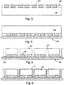
- FIGS. 2 and 3 illustrate a plurality of contact pads of devices 202 fabricated in a semiconductor wafer 200.
- a section of the semiconductor wafer 200 is shown to illustrate that a plurality of identical devices 202 may be fabricated simultaneously on a semiconductor wafer 200.
- each device 202 is shown to have two contact pads 204.
- the device 202 may have different number of contact pads depending on the type of device. For example, if the device 202 is a diode, two contact pads are necessary. However, if the device 202 is a complex circuit having a plurality of components, the number of contact pads in each device may vary.
- An isolation layer 206 is formed over the surface of the semiconductor wafer 200.
- the isolation layer 206 may be made of a polyimide or a similar polymer that offers similar electrical isolation characteristics and strength. In some embodiments, silicon oxide may be used.
- FIG. 3 shows the semiconductor wafer 200 after a portion of isolation layer 206 has been etched to expose surfaces of contact pads 204. It should be noted that well known process methods are not being described in detail so as not to obscure the present disclosure.
- FIG. 4 shows the semiconductor wafer 200 securely placed on a carrier 208.
- the carrier 208 may consist of a stack of materials, for example, a sticky foil and a buffer wafer.
- the wafer 200 is placed active side down on the carrier 208 for further processing.
- FIG. 5 depicts the semiconductor wafer 200 having trenches formed through the etching process from the backside (opposite side from the side where contact pads 204 are formed) of the semiconductor wafer 200.
- the width of each trench 210 may depend on the device type. In some applications, the width may be approximately 15-50 microns.
- the trenches 210 are in a grid pattern so as to demarcate boundaries of each device 202. The depth of the trench 210 exceeds the thickness of the semiconductor wafer 200 and less that the thickness of the semiconductor wafer 200 plus the thickness of the isolation layer 206 (remaining after etching as descripted in FIG. 5 ).
- FIG. 6 depicts a protective conformal coating over all exposed surfaces on the backside of the semiconductor wafer 200.
- Parylene is used as for the protective layer. Parylene provides a good electrical isolation, conformal step coverage and a strong bond to other materials. In other embodiments, materials that exhibits similar electrical isolation and bonding properties as Parylene may be used. It should be noted that since Parylene provides a strong adhesive bond, there is a need for the isolation layer 206 to prevent a direct contact between the Parylene and the carrier 208.
- Parylene coatings are applied at ambient temperatures with specialized vacuum deposition equipment. Parylene polymer deposition takes place at the molecular level, where films essentially 'grow' a molecule at a time. A solid, granular raw material, called dimer, is heated under vacuum and vaporized into a dimeric gas. The gas is then pyrolized to cleave the dimer to its monomeric form. In the room temperature deposition chamber, the monomer gas deposits on all surfaces as a thin, transparent polymer film. Because Parylene is applied as a gas, the coating effortlessly penetrates crevices and tight areas on multi-layer components, providing complete and uniform encapsulation. Optimal thickness of the polymer coatings is determined based on the application and the coating properties desired. While Parylene coatings can range in thickness from hundreds of angstroms to several mils, a typical thickness is in the microns range (e.g., 1 to 10 microns).
- FIG. 7 shows the semiconductor wafer 200 after the protective layer 212 is removed from horizontal surfaces through the etching process (e.g., plasma etching or chemical etching). Since the etching rate on horizontal surfaces is greater than the etching rate on vertical surfaces, the etching process is controlled to run for a selected period of time so that Parylene is removed from the horizontal surfaces (such as back of the device 202 and the bottom of the trench 210) but stays in form a thin layer on the vertical surfaces (e.g., sidewalls).
- the etching process e.g., plasma etching or chemical etching
- Parylene is not removed from the back of the device 202, a contact with tape that carries the device 202 for production and assembly may cause pick-up problems from the carrier 208 and may cause electrostatic forces so that the device 202 may stick to a cover tape during the assembly of systems that use the device 202.
- FIG. 8 shows the semiconductor wafer after further etching in the trenches 210 to singulate individual devices 202 from the semiconductor wafer 200.
- the processed described in FIG. 7 and FIG. 8 may be performed in one step using a blanket anisotropic etch to remove Parylene from the back of the semiconductor wafer 200 as well as the isolation layer 206 to make the trench 210 exposing the surface of the carrier 208 at the bottom of the trench 210.
- the protective layer 212 is remaining on the sidewalls. If the device 202 replaces the device 102 in FIG. 1 , the overflowing solder material 104 will not cause any undesirable electrical contact with other parts of the device 202, other than the contact pads.
- FIG. 9 shows the semiconductor wafer 200 being processed through an alternative embodiment in which the wafer is placed on the carrier 208 contacts 204 up (frontside up).
- the processing described in above figures can be used in the same way.
- no protective coating 212 is applied to the backside (facing the carrier 208).
- a mechanical grinding process may be used to remove the carrier 208 after applying the protective coating 212.
- FIGS 10A shows the device 202 in another embodiment.
- the etching process described in FIG. 5 is performed such that the isolation layer 206 is not etched in the well 210.
- the isolation layer 206 is either completely or partially completed etched thus producing the device 202 as shown in FIG. 10B.
- FIG. 10C shows that in some embodiments, the protective layer 212 may be left intact on the topside, as shown.
- the wafer 200 may be placed on the carrier 208 with contacts 204 up and the wells 210 may be formed by etching at the perimeters of devices 202. The etching is performed such that individual devices 202 are separated from each other. The coating 212 is then applied ever the entire wafer 200. In some embodiments, the wafer 200 may be grinded from the backside to remove the carrier 208.
- Parylene is used in the above description as example only in that in some embodiments, other materials with similar mechanical and adhesive properties may be used instead of Parylene.
- PTFE polytetrafluoroethylene
- Parylene may be used instead of Parylene.
Landscapes
- Container, Conveyance, Adherence, Positioning, Of Wafer (AREA)
- Dicing (AREA)
Applications Claiming Priority (1)
| Application Number | Priority Date | Filing Date | Title |
|---|---|---|---|
| US15/183,940 US9806034B1 (en) | 2016-06-16 | 2016-06-16 | Semiconductor device with protected sidewalls and methods of manufacturing thereof |
Publications (1)
| Publication Number | Publication Date |
|---|---|
| EP3258488A1 true EP3258488A1 (de) | 2017-12-20 |
Family
ID=58536757
Family Applications (1)
| Application Number | Title | Priority Date | Filing Date |
|---|---|---|---|
| EP17165113.6A Withdrawn EP3258488A1 (de) | 2016-06-16 | 2017-04-05 | Halbleiterbauelement mit geschützten seitenwänden |
Country Status (3)
| Country | Link |
|---|---|
| US (1) | US9806034B1 (de) |
| EP (1) | EP3258488A1 (de) |
| CN (2) | CN107527878A (de) |
Families Citing this family (2)
| Publication number | Priority date | Publication date | Assignee | Title |
|---|---|---|---|---|
| WO2021263059A1 (en) * | 2020-06-24 | 2021-12-30 | Hzo, Inc. | Gasketing and plasma ashing for coated devices |
| FR3165378A1 (fr) * | 2024-07-31 | 2026-02-06 | Stmicroelectronics International N.V. | Puces électroniques |
Citations (4)
| Publication number | Priority date | Publication date | Assignee | Title |
|---|---|---|---|---|
| US20100081235A1 (en) * | 2006-11-27 | 2010-04-01 | Yuji Furumura | Method for manufacturing rf powder |
| US20100283127A1 (en) * | 2007-06-29 | 2010-11-11 | Juergen Leib | Method for packing semiconductor components and product produced according to the method |
| US20120181640A1 (en) * | 2011-01-17 | 2012-07-19 | Von Koblinski Carsten | Semiconductor Devices Having Insulating Substrates and Methods of Formation Thereof |
| US20150364425A1 (en) * | 2011-10-28 | 2015-12-17 | Intel Corporation | 3d interconnect structure comprising through-silicon vias combined with fine pitch backside metal redistribution lines fabricated using a dual damascene type approach |
Family Cites Families (4)
| Publication number | Priority date | Publication date | Assignee | Title |
|---|---|---|---|---|
| US7169691B2 (en) * | 2004-01-29 | 2007-01-30 | Micron Technology, Inc. | Method of fabricating wafer-level packaging with sidewall passivation and related apparatus |
| KR100679684B1 (ko) * | 2006-02-16 | 2007-02-06 | 삼성전자주식회사 | 외곽에 보호층이 형성된 웨이퍼 레벨 반도체 소자 제조방법 |
| US9508623B2 (en) * | 2014-06-08 | 2016-11-29 | UTAC Headquarters Pte. Ltd. | Semiconductor packages and methods of packaging semiconductor devices |
| CN104201114A (zh) * | 2014-08-26 | 2014-12-10 | 江阴长电先进封装有限公司 | 一种侧壁绝缘保护的芯片封装方法及其封装结构 |
-
2016
- 2016-06-16 US US15/183,940 patent/US9806034B1/en active Active
-
2017
- 2017-04-05 EP EP17165113.6A patent/EP3258488A1/de not_active Withdrawn
- 2017-06-15 CN CN201710461354.XA patent/CN107527878A/zh active Pending
- 2017-06-15 CN CN202311761832.0A patent/CN117524984A/zh active Pending
Patent Citations (4)
| Publication number | Priority date | Publication date | Assignee | Title |
|---|---|---|---|---|
| US20100081235A1 (en) * | 2006-11-27 | 2010-04-01 | Yuji Furumura | Method for manufacturing rf powder |
| US20100283127A1 (en) * | 2007-06-29 | 2010-11-11 | Juergen Leib | Method for packing semiconductor components and product produced according to the method |
| US20120181640A1 (en) * | 2011-01-17 | 2012-07-19 | Von Koblinski Carsten | Semiconductor Devices Having Insulating Substrates and Methods of Formation Thereof |
| US20150364425A1 (en) * | 2011-10-28 | 2015-12-17 | Intel Corporation | 3d interconnect structure comprising through-silicon vias combined with fine pitch backside metal redistribution lines fabricated using a dual damascene type approach |
Also Published As
| Publication number | Publication date |
|---|---|
| CN117524984A (zh) | 2024-02-06 |
| US9806034B1 (en) | 2017-10-31 |
| CN107527878A (zh) | 2017-12-29 |
Similar Documents
| Publication | Publication Date | Title |
|---|---|---|
| CN103779241B (zh) | 晶片级芯片规模封装(wlcsp)的保护 | |
| CN110473858B (zh) | 半导体封装及其制造方法 | |
| US7833881B2 (en) | Methods for fabricating semiconductor components and packaged semiconductor components | |
| US20140057411A1 (en) | Dicing before grinding after coating | |
| CN106057688A (zh) | 具有屏蔽件的集成电路封装系统及其制造方法 | |
| US9281182B2 (en) | Pre-cut wafer applied underfill film | |
| CN106935571A (zh) | 具有电磁干扰屏蔽的电子封装体及相关联方法 | |
| TWI601218B (zh) | 具有高溫塗層之晶片封裝構造之製造方法 | |
| US10930541B2 (en) | Method of forming a chip arrangement, chip arrangement, method of forming a chip package, and chip package | |
| TW201635361A (zh) | 半導體裝置之製造方法 | |
| US9431334B2 (en) | Semiconductor device having single layer substrate and method | |
| US20170256432A1 (en) | Overmolded chip scale package | |
| US9806034B1 (en) | Semiconductor device with protected sidewalls and methods of manufacturing thereof | |
| US9613904B2 (en) | Semiconductor structure and manufacturing method thereof | |
| US9406818B2 (en) | Chip package and method of manufacturing the same | |
| US9365415B2 (en) | Compact electronic package with MEMS IC and related methods | |
| US20170084490A1 (en) | Method for making ic with stepped sidewall and related ic devices | |
| EP3367430B1 (de) | Verfahren zur herstellung eines halbleiterbauelementes mit sechsseitig geschützten wänden | |
| US8709877B2 (en) | Integrated circuit packaging system with an encapsulation and method of manufacture thereof | |
| WO2012135243A1 (en) | Pre-grooving for wafer applied underfill film | |
| KR20140137535A (ko) | 집적회로 패키지 제조방법 |
Legal Events
| Date | Code | Title | Description |
|---|---|---|---|
| PUAI | Public reference made under article 153(3) epc to a published international application that has entered the european phase |
Free format text: ORIGINAL CODE: 0009012 |
|
| AK | Designated contracting states |
Kind code of ref document: A1 Designated state(s): AL AT BE BG CH CY CZ DE DK EE ES FI FR GB GR HR HU IE IS IT LI LT LU LV MC MK MT NL NO PL PT RO RS SE SI SK SM TR |
|
| AX | Request for extension of the european patent |
Extension state: BA ME |
|
| STAA | Information on the status of an ep patent application or granted ep patent |
Free format text: STATUS: THE APPLICATION IS DEEMED TO BE WITHDRAWN |
|
| 18D | Application deemed to be withdrawn |
Effective date: 20180621 |