EP3255040A1 - Composé ayant une structure de noyau indénocarbazole et dispositif électroluminescent organique - Google Patents
Composé ayant une structure de noyau indénocarbazole et dispositif électroluminescent organique Download PDFInfo
- Publication number
- EP3255040A1 EP3255040A1 EP17001154.8A EP17001154A EP3255040A1 EP 3255040 A1 EP3255040 A1 EP 3255040A1 EP 17001154 A EP17001154 A EP 17001154A EP 3255040 A1 EP3255040 A1 EP 3255040A1
- Authority
- EP
- European Patent Office
- Prior art keywords
- substituted
- compound
- organic
- layer
- mixture
- Prior art date
- Legal status (The legal status is an assumption and is not a legal conclusion. Google has not performed a legal analysis and makes no representation as to the accuracy of the status listed.)
- Withdrawn
Links
- SZLKBVDKWZQGCB-UHFFFAOYSA-N C1=CC(c2cc3c(ccc(-c4ccc(-c5cnccc5)nc4)c4)c4c(ccc(-c4ccc(-c5cnccc5)nc4)c4)c4c3cc2)=CNC1c1cccnc1 Chemical compound C1=CC(c2cc3c(ccc(-c4ccc(-c5cnccc5)nc4)c4)c4c(ccc(-c4ccc(-c5cnccc5)nc4)c4)c4c3cc2)=CNC1c1cccnc1 SZLKBVDKWZQGCB-UHFFFAOYSA-N 0.000 description 1
- YXBSPEDTBVJVAY-UHFFFAOYSA-N C1=CN=[I]C=C1 Chemical compound C1=CN=[I]C=C1 YXBSPEDTBVJVAY-UHFFFAOYSA-N 0.000 description 1
- DNGHOAGNKVBWHS-UHFFFAOYSA-O C1=C[NH+]=C[I]=C1 Chemical compound C1=C[NH+]=C[I]=C1 DNGHOAGNKVBWHS-UHFFFAOYSA-O 0.000 description 1
- UMDLNDSIHJUYAH-UHFFFAOYSA-N C1[N-]C(c2ccncc2)=CC=C1c1cc2c(cccc3)c3c(cc(cc3)-c(cc4)cnc4-c4ccncc4)c3c2cc1 Chemical compound C1[N-]C(c2ccncc2)=CC=C1c1cc2c(cccc3)c3c(cc(cc3)-c(cc4)cnc4-c4ccncc4)c3c2cc1 UMDLNDSIHJUYAH-UHFFFAOYSA-N 0.000 description 1
- YMARVBSZZBTUBQ-UHFFFAOYSA-N CC1(C=NC(c2ccc(c3ccccc3c(cc3C)c4cc3-c(cc3)ncc3-c3ccccn3)c4c2)=CC1)c1ccccn1 Chemical compound CC1(C=NC(c2ccc(c3ccccc3c(cc3C)c4cc3-c(cc3)ncc3-c3ccccn3)c4c2)=CC1)c1ccccn1 YMARVBSZZBTUBQ-UHFFFAOYSA-N 0.000 description 1
Images


Classifications
-
- C—CHEMISTRY; METALLURGY
- C07—ORGANIC CHEMISTRY
- C07D—HETEROCYCLIC COMPOUNDS
- C07D213/00—Heterocyclic compounds containing six-membered rings, not condensed with other rings, with one nitrogen atom as the only ring hetero atom and three or more double bonds between ring members or between ring members and non-ring members
- C07D213/02—Heterocyclic compounds containing six-membered rings, not condensed with other rings, with one nitrogen atom as the only ring hetero atom and three or more double bonds between ring members or between ring members and non-ring members having three double bonds between ring members or between ring members and non-ring members
- C07D213/04—Heterocyclic compounds containing six-membered rings, not condensed with other rings, with one nitrogen atom as the only ring hetero atom and three or more double bonds between ring members or between ring members and non-ring members having three double bonds between ring members or between ring members and non-ring members having no bond between the ring nitrogen atom and a non-ring member or having only hydrogen or carbon atoms directly attached to the ring nitrogen atom
- C07D213/06—Heterocyclic compounds containing six-membered rings, not condensed with other rings, with one nitrogen atom as the only ring hetero atom and three or more double bonds between ring members or between ring members and non-ring members having three double bonds between ring members or between ring members and non-ring members having no bond between the ring nitrogen atom and a non-ring member or having only hydrogen or carbon atoms directly attached to the ring nitrogen atom containing only hydrogen and carbon atoms in addition to the ring nitrogen atom
- C07D213/22—Heterocyclic compounds containing six-membered rings, not condensed with other rings, with one nitrogen atom as the only ring hetero atom and three or more double bonds between ring members or between ring members and non-ring members having three double bonds between ring members or between ring members and non-ring members having no bond between the ring nitrogen atom and a non-ring member or having only hydrogen or carbon atoms directly attached to the ring nitrogen atom containing only hydrogen and carbon atoms in addition to the ring nitrogen atom containing two or more pyridine rings directly linked together, e.g. bipyridyl
-
- C—CHEMISTRY; METALLURGY
- C09—DYES; PAINTS; POLISHES; NATURAL RESINS; ADHESIVES; COMPOSITIONS NOT OTHERWISE PROVIDED FOR; APPLICATIONS OF MATERIALS NOT OTHERWISE PROVIDED FOR
- C09K—MATERIALS FOR MISCELLANEOUS APPLICATIONS, NOT PROVIDED FOR ELSEWHERE
- C09K11/00—Luminescent, e.g. electroluminescent, chemiluminescent materials
- C09K11/06—Luminescent, e.g. electroluminescent, chemiluminescent materials containing organic luminescent materials
-
- H—ELECTRICITY
- H05—ELECTRIC TECHNIQUES NOT OTHERWISE PROVIDED FOR
- H05B—ELECTRIC HEATING; ELECTRIC LIGHT SOURCES NOT OTHERWISE PROVIDED FOR; CIRCUIT ARRANGEMENTS FOR ELECTRIC LIGHT SOURCES, IN GENERAL
- H05B33/00—Electroluminescent light sources
- H05B33/12—Light sources with substantially two-dimensional radiating surfaces
- H05B33/14—Light sources with substantially two-dimensional radiating surfaces characterised by the chemical or physical composition or the arrangement of the electroluminescent material, or by the simultaneous addition of the electroluminescent material in or onto the light source
-
- H—ELECTRICITY
- H10—SEMICONDUCTOR DEVICES; ELECTRIC SOLID-STATE DEVICES NOT OTHERWISE PROVIDED FOR
- H10K—ORGANIC ELECTRIC SOLID-STATE DEVICES
- H10K50/00—Organic light-emitting devices
- H10K50/10—OLEDs or polymer light-emitting diodes [PLED]
- H10K50/11—OLEDs or polymer light-emitting diodes [PLED] characterised by the electroluminescent [EL] layers
-
- H—ELECTRICITY
- H10—SEMICONDUCTOR DEVICES; ELECTRIC SOLID-STATE DEVICES NOT OTHERWISE PROVIDED FOR
- H10K—ORGANIC ELECTRIC SOLID-STATE DEVICES
- H10K50/00—Organic light-emitting devices
- H10K50/10—OLEDs or polymer light-emitting diodes [PLED]
- H10K50/14—Carrier transporting layers
- H10K50/16—Electron transporting layers
- H10K50/165—Electron transporting layers comprising dopants
-
- H—ELECTRICITY
- H10—SEMICONDUCTOR DEVICES; ELECTRIC SOLID-STATE DEVICES NOT OTHERWISE PROVIDED FOR
- H10K—ORGANIC ELECTRIC SOLID-STATE DEVICES
- H10K50/00—Organic light-emitting devices
- H10K50/10—OLEDs or polymer light-emitting diodes [PLED]
- H10K50/17—Carrier injection layers
- H10K50/171—Electron injection layers
-
- H—ELECTRICITY
- H10—SEMICONDUCTOR DEVICES; ELECTRIC SOLID-STATE DEVICES NOT OTHERWISE PROVIDED FOR
- H10K—ORGANIC ELECTRIC SOLID-STATE DEVICES
- H10K85/00—Organic materials used in the body or electrodes of devices covered by this subclass
- H10K85/60—Organic compounds having low molecular weight
- H10K85/615—Polycyclic condensed aromatic hydrocarbons, e.g. anthracene
- H10K85/622—Polycyclic condensed aromatic hydrocarbons, e.g. anthracene containing four rings, e.g. pyrene
-
- H—ELECTRICITY
- H10—SEMICONDUCTOR DEVICES; ELECTRIC SOLID-STATE DEVICES NOT OTHERWISE PROVIDED FOR
- H10K—ORGANIC ELECTRIC SOLID-STATE DEVICES
- H10K85/00—Organic materials used in the body or electrodes of devices covered by this subclass
- H10K85/60—Organic compounds having low molecular weight
- H10K85/615—Polycyclic condensed aromatic hydrocarbons, e.g. anthracene
- H10K85/626—Polycyclic condensed aromatic hydrocarbons, e.g. anthracene containing more than one polycyclic condensed aromatic rings, e.g. bis-anthracene
-
- H—ELECTRICITY
- H10—SEMICONDUCTOR DEVICES; ELECTRIC SOLID-STATE DEVICES NOT OTHERWISE PROVIDED FOR
- H10K—ORGANIC ELECTRIC SOLID-STATE DEVICES
- H10K85/00—Organic materials used in the body or electrodes of devices covered by this subclass
- H10K85/60—Organic compounds having low molecular weight
- H10K85/631—Amine compounds having at least two aryl rest on at least one amine-nitrogen atom, e.g. triphenylamine
-
- H—ELECTRICITY
- H10—SEMICONDUCTOR DEVICES; ELECTRIC SOLID-STATE DEVICES NOT OTHERWISE PROVIDED FOR
- H10K—ORGANIC ELECTRIC SOLID-STATE DEVICES
- H10K85/00—Organic materials used in the body or electrodes of devices covered by this subclass
- H10K85/60—Organic compounds having low molecular weight
- H10K85/649—Aromatic compounds comprising a hetero atom
- H10K85/654—Aromatic compounds comprising a hetero atom comprising only nitrogen as heteroatom
-
- C—CHEMISTRY; METALLURGY
- C07—ORGANIC CHEMISTRY
- C07D—HETEROCYCLIC COMPOUNDS
- C07D273/00—Heterocyclic compounds containing rings having nitrogen and oxygen atoms as the only ring hetero atoms, not provided for by groups C07D261/00 - C07D271/00
-
- C—CHEMISTRY; METALLURGY
- C07—ORGANIC CHEMISTRY
- C07D—HETEROCYCLIC COMPOUNDS
- C07D498/00—Heterocyclic compounds containing in the condensed system at least one hetero ring having nitrogen and oxygen atoms as the only ring hetero atoms
- C07D498/12—Heterocyclic compounds containing in the condensed system at least one hetero ring having nitrogen and oxygen atoms as the only ring hetero atoms in which the condensed system contains three hetero rings
- C07D498/18—Bridged systems
-
- C—CHEMISTRY; METALLURGY
- C09—DYES; PAINTS; POLISHES; NATURAL RESINS; ADHESIVES; COMPOSITIONS NOT OTHERWISE PROVIDED FOR; APPLICATIONS OF MATERIALS NOT OTHERWISE PROVIDED FOR
- C09K—MATERIALS FOR MISCELLANEOUS APPLICATIONS, NOT PROVIDED FOR ELSEWHERE
- C09K2211/00—Chemical nature of organic luminescent or tenebrescent compounds
- C09K2211/14—Macromolecular compounds
- C09K2211/1408—Carbocyclic compounds
- C09K2211/1425—Non-condensed systems
Definitions
- the present invention relates to compounds suited for an organic electroluminescent device (hereinafter, simply referred to as "organic EL device”), a preferred self light-emitting device for various display devices, and to the device. Specifically, the invention relates to compounds having a substituted bipyridyl and triphenylene ring structure, and to organic EL devices that use the compounds.
- organic EL device organic electroluminescent device
- the organic EL device is a self-emitting device, and has been actively studied for their brighter, superior viewability and ability to display clearer images compared with the liquid crystal device.
- Non-Patent Document 2 for example.
- the light emitting layer can also be fabricated by doping a charge-transporting compound, generally called a host material, with a phosphor or a phosphorescent material.
- a charge-transporting compound generally called a host material
- a phosphor or a phosphorescent material As described in the foregoing Non-Patent Documents 1 and 2, selection of organic materials in an organic EL device greatly influences various device characteristics, including efficiency and durability.
- the charges injected from both the electrodes recombine at the light emitting layer to cause emission.
- the holes have greater mobility than the electrons, some of the holes pass through the light emitting layer, and lower efficiency. Accordingly, there is a need for an electron transport material that has high electron mobility.
- Tris(8-hydroxyquinoline)aluminum (hereinafter, referred to simply as "Alq 3 "), a representative light-emitting material, has been commonly used as an electron transport material. However, because of the slow electron mobility and the work function of 5.6 eV, it cannot be said that this material has a sufficient hole blocking performance.
- Patent Document 3 One way of preventing some of the holes from passing through the light emitting layer and improving the probability of charge recombination at the light emitting layer is to insert a hole blocking layer.
- various hole blocking materials have been proposed, including, for example, triazole derivatives (refer to Patent Document 3, for example), bathocuproin (hereinafter, referred to simply as "BCP”), and a mixed ligand complex of aluminum [aluminum(III)bis(2-methyl-8-quinolinate)-4-phenylphenolat e (hereinafter, referred to simply as "BAlq”)] (refer to Non-Patent Document 2, for example).
- TEZ 3-(4-biphenylyl)-4-phenyl-5-(4-t-butylphenyl)-1,2,4-triazo le
- TAZ has a large work function of 6.6 eV and a high hole blocking capability, and has been used as the electron-transporting hole blocking layer laminated on the cathode side of the fluorescent layer or phosphorescent layer produced by methods such as vacuum vapor deposition and coating. TAZ has contributed to improve the efficiency of organic EL devices (refer to Non-Patent Document 3, for example).
- TAZ TAZ
- the material needs to be combined with an electron transport material of higher electron transporting property for the production of an organic EL device (refer to Non-Patent Document 4, for example).
- BCP also has a large work function of 6.7 eV and a high hole blocking capability.
- Tg low glass transition point
- BAlq a hole blocking layer
- organic compounds are needed that excel in electron injection and transport performance and hole blocking capability, and that has high stability in the thin-film state.
- Some of the physical properties of the organic compounds to be provided by the present invention include (1) good electron injection characteristics, (2) fast electron mobility, (3) high molecular orientation, and (4) excellent heat resistance. Some of the physical properties of the organic EL device to be provided by the present invention include (1) high power efficiency, (2) low turn on voltage, and (3) low actual driving voltage.
- the present inventors designed and chemically synthesized a compound by combining (i) a triphenylene ring structure having potential to provide desirable intermolecular packing in the thin-film state with its high planarity, and a desirable electron transport property with its abundant ⁇ electrons, and (ii) a bipyridyl group having high planarity and high electron affinity.
- the compound was used to fabricate various test organic EL devices, and device characteristics were evaluated to complete the present invention.
- the present invention is a compound of general formula (1) or (2) having a substituted bipyridyl and triphenylene ring structure.
- R 1 to R 18 may be the same or different, and represent a hydrogen atom, a deuterium atom, a fluorine atom, a chlorine atom, cyano, trifluoromethyl, linear or branched alkyl of 1 to 6 carbon atoms that may have a substituent, a substituted or unsubstituted aromatic hydrocarbon group, a substituted or unsubstituted aromatic heterocyclic group, or a substituted or unsubstituted condensed polycyclic aromatic group.
- n1 and n2 may be the same or different, and represent 2 or 3.
- the plurality of R 3 to R 8 may be the same or different, respectively.
- R 19 to R 39 may be the same or different, and represent a hydrogen atom, a deuterium atom, a fluorine atom, a chlorine atom, cyano, trifluoromethyl, linear or branched alkyl of 1 to 6 carbon atoms that may have a substituent, a substituted or unsubstituted aromatic hydrocarbon group, a substituted or unsubstituted aromatic heterocyclic group, or a substituted or unsubstituted condensed polycyclic aromatic group.
- n3, n4, and n5 may be the same or different, and represent 2 or 3.
- the plurality of R 22 to R 30 may be the same or different, respectively.
- the present invention is a compound of the following general formula (1') having a substituted bipyridyl and triphenylene ring structure.
- R 1 to R 18 may be the same or different, and represent a hydrogen atom, a deuterium atom, a fluorine atom, a chlorine atom, cyano, trifluoromethyl, linear or branched alkyl of 1 to 6 carbon atoms that may have a substituent, a substituted or unsubstituted aromatic hydrocarbon group, a substituted or unsubstituted aromatic heterocyclic group, or a substituted or unsubstituted condensed polycyclic aromatic group.
- n1 and n2 may be the same or different, and represent 2 or 3.
- the plurality of R 3 to R 8 may be the same or different, respectively.
- the present invention is a compound of the following general formula (1") having a substituted bipyridyl and triphenylene ring structure.
- R 1 to R 18 may be the same or different, and represent a hydrogen atom, a deuterium atom, a fluorine atom, a chlorine atom, cyano, trifluoromethyl, linear or branched alkyl of 1 to 6 carbon atoms that may have a substituent, a substituted or unsubstituted aromatic hydrocarbon group, a substituted or unsubstituted aromatic heterocyclic group, or a substituted or unsubstituted condensed polycyclic aromatic group.
- n1 and n2 may be the same or different, and represent 2 or 3.
- the plurality of R 3 to R 8 may be the same or different, respectively.
- the present invention is a compound of the following general formula (1"') having a substituted bipyridyl and triphenylene ring structure.
- R 3 to R 18 , R 40 to R 47 may be the same or different, and represent a hydrogen atom, a deuterium atom, a fluorine atom, a chlorine atom, cyano, trifluoromethyl, linear or branched alkyl of 1 to 6 carbon atoms that may have a substituent, a substituted or unsubstituted aromatic hydrocarbon group, a substituted or unsubstituted aromatic heterocyclic group, or a substituted or unsubstituted condensed polycyclic aromatic group.
- the present invention is a compound of the following general formula (1"") having a substituted bipyridyl and triphenylene ring structure.
- R 3 to R 18 , R 40 to R 47 may be the same or different, and represent a hydrogen atom, a deuterium atom, a fluorine atom, a chlorine atom, cyano, trifluoromethyl, linear or branched alkyl of 1 to 6 carbon atoms that may have a substituent, a substituted or unsubstituted aromatic hydrocarbon group, a substituted or unsubstituted aromatic heterocyclic group, or a substituted or unsubstituted condensed polycyclic aromatic group.
- the present invention is a compound of the following general formula (2') having a substituted bipyridyl and triphenylene ring structure.
- R 19 to R 39 may be the same or different, and represent a hydrogen atom, a deuterium atom, a fluorine atom, a chlorine atom, cyano, trifluoromethyl, linear or branched alkyl of 1 to 6 carbon atoms that may have a substituent, a substituted or unsubstituted aromatic hydrocarbon group, a substituted or unsubstituted aromatic heterocyclic group, or a substituted or unsubstituted condensed polycyclic aromatic group.
- n3, n4, and n5 may be the same or different, and represent 2 or 3.
- the plurality of R 22 to R 30 may be the same or different, respectively.
- the present invention is an organic EL device that includes a pair of electrodes, and one or more organic layers sandwiched between the pair of electrodes, wherein at least one of the organic layers contains the compound of any of the general formulae (1) to (1'"'), general formula (2), or general formula (2') having a substituted bipyridyl and triphenylene ring structure.
- alkyl in the "linear or branched alkyl of 1 to 6 carbon atoms that may have a substituent” represented by R 1 to R 47 in the general formulae (1) to (1''''), general formula (2), or general formula (2') include methyl, ethyl, n-propyl, isopropyl, n-butyl, isobutyl, tert-butyl, n-pentyl, isopentyl, neopentyl, and n-hexyl.
- substituted linear or branched alkyl of 1 to 6 carbon atoms represented by R 1 to R 47 in the general formulae (1) to (1''''), general formula (2), or general formula (2')
- substituents include a deuterium atom, a fluorine atom, a chlorine atom, cyano, nitro, linear or branched alkyl of 1 to 6 carbon atoms, cyclopentyl, cyclohexyl, dialkylamino substituted with linear or branched alkyl of 1 to 6 carbon atoms, phenyl, biphenylyl, terphenylyl, tetrakisphenyl, styryl, naphthyl, fluorenyl, phenanthryl, indenyl, pyrenyl, pyridyl, bipyridyl, triazyl, pyrimidyl, quinolyl, isoquinolyl, ind
- aromatic hydrocarbon group aromatic heterocyclic group
- condensed polycyclic aromatic group in the "substituted or unsubstituted aromatic hydrocarbon group", “substituted or unsubstituted aromatic heterocyclic group”, or “substituted or unsubstituted condensed polycyclic aromatic group” represented by R 1 to R 47 in the general formulae (1) to (1'''), general formula (2), or general formula (2')
- Preferred as the "substituted or unsubstituted aromatic heterocyclic group" represented by R 1 to R 8 , R 19 to R 27 , and R 40 to R 47 is substituted or unsubstituted pyridyl, because it can be expected to improve the electron injection characteristics.
- substituted aromatic hydrocarbon group substituted aromatic heterocyclic group
- substituted condensed polycyclic aromatic group represented by R 1 to R 47 in the general formulae (1) to (1"), general formula (2), or general formula (2')
- substituents in the "substituted aromatic hydrocarbon group”, “substituted aromatic heterocyclic group”, or “substituted condensed polycyclic aromatic group” represented by R 1 to R 47 in the general formulae (1) to (1""), general formula (2), or general formula (2') include a deuterium atom, a fluorine atom, a chlorine atom, cyano, trifluoromethyl, nitro, linear or branched alkyl of 1 to 6 carbon atoms, cyclopentyl, cyclohexyl, linear or branched alkoxy of 1 to 6 carbon atoms, dialkylamino substituted with linear or branched alkyl of 1 to 6 carbon atoms, phenyl, biphenylyl, terphenylyl
- the compounds of the general formulae (1) to (1""), general formula (2), or general formula (2') having a substituted bipyridyl and triphenylene ring structure of the present invention are novel compounds.
- the compounds have faster electron mobility than conventional electron transport materials, and can maintain the stable thin-film state, making it possible to improve luminous efficiency, and lower driving voltage.
- the bipyridyl bound to the triphenylene ring (when n1 to n5 are 2 in the general formula (1) or (2)) is preferably 2,2'-bipyridyl, 2,3'-bipyridyl, 2,4'-bipyridyl, or 3,2'-bipyridyl, particularly preferably 2,2'-bipyridyl, or a 2,4'-bipyridyl.
- the compounds of the general formulae (1) to (1""), general formula (2), or general formula (2') having a substituted bipyridyl and triphenylene ring structure of the present invention can be used as the constituent material of the electron injection layer and/or the electron transport layer of an organic EL device.
- the efficiency of the electron transport from the electron transport layer to the light emitting layer improves. This improves the luminous efficiency, and lowers driving voltage, making it possible to improve the durability of the organic EL device.
- the compounds of the general formulae (1) to (1""), general formula (2), or general formula (2') having a substituted bipyridyl and triphenylene ring structure of the present invention also can be used as the constituent material of the light emitting layer of an organic EL device.
- the material of the present invention having a more desirable electron transport property and a wider band gap than conventional materials can provide an organic EL device of low driving voltage and improved luminous efficiency.
- the organic EL device of the present invention can realize high efficiency and high durability, because it uses the compound having a substituted bipyridyl and triphenylene ring structure that has faster electron mobility and a more stable thin-film state than conventional electron transport materials.
- the compounds having a substituted bipyridyl and triphenylene ring structure of the present invention have fast electron mobility and a stable thin-film state, and are useful as the constituent material of the electron injection layer, the electron transport layer, or the light emitting layer of an organic EL device.
- the organic EL device produced by using the compounds having a substituted bipyridyl and triphenylene ring structure can have improved luminous efficiency and low driving voltage, and can thus have improved durability.
- the compounds having a substituted bipyridyl and triphenylene ring structure of the present invention are novel compounds, and may be synthesized by using, for example, the following method.
- the dihalide of a corresponding triphenylene compound is boronated with a compound such as bis(pinacolato)diboron to synthesize a corresponding borate product (refer to Non-Patent Document 5, for example), and this corresponding borate product is reacted with a halogenobipyridine having various substituents in a cross-coupling reaction such as Suzuki coupling (refer to Non-Patent Document 6, for example) to synthesize the compound having a substituted bipyridyl and triphenylene ring structure.
- a cross-coupling reaction such as Suzuki coupling
- the compounds having a substituted bipyridyl and triphenylene ring structure also can be synthesized as follows. First, a halogenobipyridine having various substituents is boronated with a compound such as bis (pinacolato) diboron, and the resulting bipyridine borate product with various substituents is then reacted with the dihalide of a corresponding triphenylene compound in a cross-coupling reaction such as Suzuki coupling.
- a cross-coupling reaction such as Suzuki coupling.
- These compounds were purified by methods such as column chromatography, adsorption using, for example, a silica gel, activated carbon, or activated clay, and recrystallization or crystallization using a solvent.
- the compounds were identified by using methods such as NMR analysis, mass spectrometry, and elementary analysis. Melting point, glass transition point (Tg), and work function were taken for the measurement of physical properties. Melting point can be used as an index of ease of vapor deposition, glass transition point (Tg) as an index of stability in the thin-film state, and the work function as an index of hole blocking capability.
- the melting point and the glass transition point (Tg) were measured using a powder, using a high-sensitive differential scanning calorimeter DSC3100S (Bruker AXS).
- a 100 nm-thick thin film was fabricated on an ITO substrate, and an atmosphere photoelectron spectrometer (AC-3; Riken Keiki Co., Ltd.) was used.
- the organic EL device of the present invention may have a structure including an anode, a hole transport layer, a light emitting layer, a hole blocking layer, an electron transport layer, and a cathode successively formed on a substrate, optionally with a hole injection layer between the anode and the hole transport layer, an electron injection layer between the electron transport layer and the cathode, or an electron blocking layer between the light emitting layer and the hole transport layer.
- Some of the organic layers in this multilayer structure may be omitted.
- the organic EL device may be configured to include an anode, a hole transport layer, a light emitting layer, an electron transport layer, and a cathode successively formed on a substrate.
- Each of the light emitting layer, the hole transport layer, and the electron transport layer may have a laminate structure of two or more layers.
- Electrode materials with a large work function such as ITO and gold, are used as the anode of the organic EL device of the present invention.
- the hole injection layer of the organic EL device of the present invention may be made of various materials, including, for example, porphyrin compounds as represented by copper phthalocyanine, starburst-type triphenylamine derivatives, triphenylamine trimers and tetramers such as an arylamine compound of a structure in which three or more triphenylamine structures are joined to each other within the molecule via a single bond or a divalent group that does not contain a heteroatom, accepting heterocyclic compounds such as hexacyano azatriphenylene, and coating- type polymer materials.
- These materials may be formed into a thin film by using a vapor deposition method, or other known methods such as spin coating and an inkjet method.
- Examples of the material used for the hole transport layer of the organic EL device of the present invention include benzidine derivatives [such as N,N'-diphenyl-N,N'-di (m-tolyl)-benzidine (hereinafter, referred to simply as "TPD”), N,N'-diphenyl-N,N'-di( ⁇ -naphthyl)-benzidine (hereinafter, referred to simply as "NPD”), and N,N,N',N'-tetrabiphenylylbenzidine], 1,1-bis[(di-4-tolylamino)phenyl]cyclohexane (hereinafter, referred to simply as "TAPC”), various triphenylamine trimers and tetramers, and carbazole derivatives.
- TPD N,N'-diphenyl-N,N'-di (m-tolyl)-benzidine
- NPD N,N'-diphenyl-N,N'-d
- PEDOT poly(3,4-ethylenedioxythiophene)
- PSS poly(styrene sulfonate)
- the hole injection layer or the hole transport layer may be one obtained by the P-doping of material such as trisbromophenylamine hexachloroantimony in the material commonly used for these layers.
- material such as trisbromophenylamine hexachloroantimony in the material commonly used for these layers.
- polymer compounds having a TPD structure as a part of the compound structure also may be used.
- Examples of the material used for the electron blocking layer of the organic EL device of the present invention include compounds having an electron blocking effect, including, for example, carbazole derivatives such as 4,4',4''-tri(N-carbazolyl)triphenylamine (hereinafter, simply "TCTA”), 9,9-bis[4-(carbazol-9-yl)phenyl]fluorene, 1,3-bis(carbazol-9-yl)benzene (hereinafter, simply “mCP”), and 2,2-bis(4-carbazol-9-ylphenyl)adamantane (hereinafter, simply "Ad-Cz”); and compounds having a triphenylsilyl group and a triarylamine structure, as represented by 9-[4-(carbazol-9-yl)phenyl]-9-[4-(triphenylsilyl)phenyl]-9 H-fluorene.
- carbazole derivatives such as 4,4',4''-tri(N-car
- These may be deposited alone, or may be used as a single layer deposited as a mixture with other materials, or as a laminate of individually deposited layers, a laminate of a layer deposited as a mixture, or a laminate of a layer deposited alone and a layer deposited as a mixture.
- These materials may be formed into a thin-film by using a vapor deposition method, or other known methods such as spin coating and an inkjet method.
- Examples of the material used for the light emitting layer of the organic EL device of the present invention include quinolinol derivative metal complexes such as Alq 3 , various metal complexes, anthracene derivatives, bis(styryl)benzene derivatives, pyrene derivatives, oxazole derivatives, and polyparaphenylene vinylene derivatives, in addition to the compounds having a substituted bipyridyl and triphenylene ring structure of the present invention.
- the light emitting layer may be configured from a host material and a dopant material.
- Examples of the host material include thiazole derivatives, benzimidazole derivatives, and polydialkyl fluorene derivatives, in addition to the foregoing light-emitting materials.
- Examples of the dopant material include quinacridone, coumalin, rubrene, perylene, derivatives thereof, benzopyran derivatives, rhodamine derivatives, and aminostyryl derivatives. These may be deposited alone, or may be used as a single layer deposited as a mixture with other materials, or as a laminate of individually deposited layers, a laminate of layers deposited as a mixture, or a laminate of a layer deposited alone and a layer deposited as a mixture.
- the light-emitting material may be phosphorescent light-emitting material.
- Phosphorescent materials as metal complexes of metals such as iridium and platinum may be used as the phosphorescent light-emitting material.
- the phosphorescent materials include green phosphorescent materials such as Ir(ppy) 3 , blue phosphorescent materials such as FIrpic and FIr 6 , and red phosphorescent materials such as Btp 2 Ir(acac).
- carbazole derivatives such as 4,4'-di(N-carbazolyl)biphenyl (hereinafter, simply "CBP"), TCTA, and mCP may be used as the hole injecting and transporting host material.
- the doping of the phosphorescent light-emitting material in the host material should preferably be made by co-evaporation in a range of 1 to 30 weight percent with respect to the whole light emitting layer.
- These materials may be formed into a thin-film by using a vapor deposition method, or other known methods such as spin coating and an inkjet method.
- the hole blocking layer of the organic EL device of the present invention may be formed by using hole blocking compounds such as various rare earth complexes, oxazole derivatives, triazole derivatives, and triazine derivatives, in addition to the compounds having a substituted bipyridyl and triphenylene ring structure of present invention, and metal complexes of phenanthroline derivatives such as bathocuproin (hereinafter, simply "BCP"), and metal complexes of quinolinol derivatives such as BAlq. These materials may also serve as the material of the electron transport layer.
- hole blocking compounds such as various rare earth complexes, oxazole derivatives, triazole derivatives, and triazine derivatives, in addition to the compounds having a substituted bipyridyl and triphenylene ring structure of present invention, and metal complexes of phenanthroline derivatives such as bathocuproin (hereinafter, simply "BCP"), and metal complexes of quinolinol derivatives such
- These may be deposited alone, or may be used as a single layer deposited as a mixture with other materials, or as a laminate of individually deposited layers, a laminate of layers deposited as a mixture, or a laminate of a layer deposited alone and a layer deposited as a mixture.
- These materials may be formed into a thin-film by using a vapor deposition method, or other known methods such as spin coating and an inkjet method.
- Examples of the material used for the electron transport layer of the organic EL device of the present invention include various metal complexes, triazole derivatives, triazine derivatives, oxadiazole derivatives, thiadiazole derivatives, carbodiimide derivatives, quinoxaline derivatives, phenanthroline derivatives, and silole derivatives, in addition to the compounds having a substituted bipyridyl and triphenylene ring structure of the present invention, and quinolinol derivative metal complexes such as Alq 3 and BAlq.
- These may be deposited alone, or may be used as a single layer deposited as a mixture with other materials, or as a laminate of individually deposited layers, a laminate of layers deposited as a mixture, or a laminate of a layer deposited alone and a layer deposited as a mixture.
- These materials may be formed into a thin-film by using a vapor deposition method, or other known methods such as spin coating and an inkjet method.
- Examples of the material used for the electron injection layer of the organic EL device of the present invention include alkali metal salts (such as lithium fluoride, and cesium fluoride), alkaline earth metal salts (such as magnesium fluoride), and metal oxides (such as aluminum oxide), in addition to the compounds having a substituted bipyridyl and triphenylene ring structure of the present invention.
- the electron injection layer may be omitted upon preferably selecting the electron transport layer and the cathode.
- the electron injection layer or the electron transport layer may be one obtained by the N-doping of metals such as cesium in the materials commonly used for these layers.
- the cathode of the organic EL device of the present invention may be made of an electrode material having a low work function (such as aluminum), or an alloy of an electrode material having an even lower work function (such as a magnesium-silver alloy, a magnesium-indium alloy, or an aluminum-magnesium alloy).
- a low work function such as aluminum
- an alloy of an electrode material having an even lower work function such as a magnesium-silver alloy, a magnesium-indium alloy, or an aluminum-magnesium alloy.
- 2,5-Dibromopyridine (19.5 g), 2-pyridylzinc bromide (150 ml), tetrahydrofuran (90 ml), and tetrakis (triphenylphosphine) palladium (0) (4.33 g) were added to a nitrogen-substituted reaction vessel. After being cooled, the mixture was stirred at 0°C for 2 hours, and then at room temperature for 3 hours. The reaction mixture was added to a 10% disodium dihydrogen ethylenediamine tetraacetate aqueous solution, and stirred for 6 hours. The organic layer was collected by separation after adding chloroform (300 ml) .
- the organic layer was dried over anhydrous magnesium sulfate, and concentrated to obtain a crude product.
- the crude product was purified by column chromatography (support: silica gel, eluent: toluene) to obtain a white powder of 5-bromo-2,2'-bipyridine (11.1 g; yield 63%).
- 1,2-diiodobenzene (24.4 g), 3-trimethylsilylphenylboronic acid (30 g), sodium hydroxide (8.8 g), tetrakis(triphenylphosphine)palladium(0) (4.3 g), diethylene glycol dimethyl ether (160 ml), and water (40 ml) were added to a nitrogen-substituted reaction vessel.
- the mixture was heated, and stirred at 95°C for 15 hours. After cooling the mixture to room temperature, water (100 ml) was added, and the organic layer was collected by separation. The organic layer was washed two times with water (100 ml), dried over anhydrous magnesium sulfate, and concentrated to obtain a crude product.
- the crude product was purified by column chromatography (support: silica gel, eluent: n-hexane) to obtain a white powder of 3,3"-bis(trimethylsilyl)-1,1':2',1"-terphenyl (23.3 g; yield 84%).
- the structure of the product yellow powder was identified by NMR.
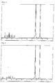
- the 1 H-NMR measurement result is shown in FIG. 1 .
- 2,6-Dibromopyridine (19.5 g), 2-pyridylzinc bromide (150 ml), tetrahydrofuran (90 ml), and tetrakis(triphenylphosphine)palladium(0) (4.33 g) were added to a nitrogen-substituted reaction vessel. The mixture was cooled, and stirred at 0°C for 2 hours, and then at room temperature for 3 hours. The reaction mixture was added to a 10% disodium dihydrogen ethylenediamine tetraacetate aqueous solution, and stirred for 6 hours. The organic layer was collected by separation after adding chloroform (300 ml) .
- the organic layer was dried over anhydrous magnesium sulfate, and concentrated to obtain a crude product.
- the crude product was purified by column chromatography (support: silica gel, eluent: toluene) to obtain a white powder of 6-bromo-2,2'-bipyridine (11.1 g; yield 63%).
- the structure of the product pale yellowish white powder was identified by NMR.
- the 1 H-NMR measurement result is shown in FIG. 2 .
- triphenylene-2,11-diol (1.25 g), N-phenyl-bis(trifluoromethanesulfoneimide) (6.87 g), sodium carbonate (5.1 g), and dimethylformamide (50 ml) were added to a nitrogen-substituted reaction vessel, and the mixture was stirred at room temperature for 12 hours. After adding water (50 ml) to the reaction mixture, the mixture was stirred for 30 minutes, and the precipitate was collected by filtration. The precipitate was washed with methanol to obtain a white powder of triphenylene-2,11-diyl-bis(trifluoromethanesulfonate) (2.38 g; yield 91%).
- triphenylene-2,11-diyl-bis(trifluoromethanesulfonate) (2.3 g), bis (pinacolato) diboron (2.5 g), potassium acetate (1.3 g), 1,4-dioxane (50 ml) predried with a 4A molecular sieve, and a [1,1'-bis(diphenylphosphino)ferrocene]palladium(II)dichlor ide-dichloromethane complex (1:1; 0.1 g) were added to a nitrogen-substituted reaction vessel. The mixture was heated, and stirred at 80°C for 10 hours.
- the structure of the product yellow powder was identified by NMR.
- the 1 H-NMR measurement result is shown in FIG. 3 .
- the structure of the product pale yellowish white powder was identified by NMR.
- the 1 H-NMR measurement result is shown in FIG. 4 .
- 2,5-Dibromopyridine (9.6 g), 4-pyridineboronic acid (2.5 g), toluene (50 ml), ethanol (40 ml), a 2 M potassium carbonate aqueous solution (15.2 ml), and tetrakis(triphenylphosphine)palladium(0) (1.50 g) were added to a nitrogen-substituted reaction vessel. The mixture was heated, and refluxed for 24 hours while being stirred. After cooling the mixture to room temperature, chloroform (500 ml) and water (300 ml) were added, and the organic layer was collected by separation.
- the structure of the pale yellowish white powder was identified by using a matrix-assisted laser desorption/ionization time-of-flight mass spectrometer (AXIMA-CFR Plus; Shimadzu Corporation), and an elementary analysis device (Yanaco CHNCORDER MT-5; Yanamoto Seisakusho).
- MS (m/z) 537 [calculated value (m/z) 536.20], elementary analysis, measured value: C;85.08, H;4.42, N;10.39, calculated value (C 38 H 24 N 4 ): C;85.05, H;4.51, N;10.44.
- 1,2-Diiodobenzene (20 g), 4-trimethylsilylphenylboronic acid (25 g), sodium hydroxide (7.4 g), tetrakis(triphenylphosphine)palladium(0) (3.6 g), diethylene glycol dimethyl ether (240 ml), and water (60 ml) were added to a nitrogen-substituted reaction vessel. The mixture was heated, and stirred at 95°C for 15 hours. Water (100 ml) was added after cooling the mixture to room temperature, and the organic layer was collected by separation. The organic layer was washed two times with water (100 ml), dried over anhydrous magnesium sulfate, and concentrated to obtain a crude product.
- the crude product was purified by column chromatography (support: silica gel, eluent: n-hexane) to obtain a white powder of 4,4"-bis(trimethylsilyl)-1,1':2',1"-terphenyl (21.1 g; yield 93%).
- the melting points and the glass transition points of the compounds of the present invention were determined using a high-sensitive differential scanning calorimeter (DSC 3100S; Bruker AXS). Melting point Glass transition point Compound of Example 1 of the present invention 338°C None Compound of Example 2 of the present invention 285°C None
- the compounds of the present invention were not shown to have glass transition points. This indicates that the compounds of the present invention have a stable thin-film state.
- a 50 nm-thick vapor-deposited film was fabricated on an ITO substrate using the compounds of the present invention.
- the work function was measured using an atmosphere photoelectron spectrometer (Model AC-3 produced by Riken Keiki Co., Ltd.).
- Work function Compound of Example 1 of the present invention 5.74 eV Compound of Example 2 of the present invention 5.69 eV Compound of Example 3 of the present invention 5.82 eV Compound of Example 4 of the present invention 5.73 eV Compound of Example 5 of the present invention 6.21 eV
- the compounds of the present invention have work functions greater than the work function 5.4 eV of common hole transport materials such as NPD and TPD, and have high hole blocking capability.
- the organic EL device as illustrated in FIG. 5 , was fabricated from a hole transport layer 3, a light emitting layer 4, an electron transport layer 5, an electron injection layer 6, and a cathode (silver electrode) 7 successively formed by vapor deposition on a glass substrate 1 that had been provided beforehand with an ITO electrode as a transparent anode 2.
- the glass substrate 1 having ITO (thickness 100 nm) formed thereon was washed with an organic solvent, and subjected to a UV ozone treatment to wash the surface.
- the glass substrate with the ITO electrode was then installed, in a vacuum vapor deposition apparatus, and the pressure was reduced to 0.001 Pa or less.
- the light emitting layer 4 was then formed on the hole transport layer 3 by forming Alq 3 in a thickness of 20 nm at a deposition rate of 2 ⁇ /s.
- the electron transport layer 5 was formed on the light emitting layer 4 by forming the compound of Example 1 of the present invention (compound 3) in a thickness of 30 nm at a deposition rate of 2 ⁇ /s.
- the electron injection layer 6 was then formed on the electron transport layer 5 by forming a magnesium silver alloy in a thickness of 100 nm at a deposition rate of 3.3 ⁇ /s.
- the cathode 7 was formed by vapor depositing silver in a thickness of 10 nm. The characteristics of the organic EL device thus fabricated were measured in an atmosphere at ordinary temperature.
- Table 1 summarizes the results of the emission characteristics measurements performed by applying a DC voltage to the organic EL device fabricated with the compound of Example 1 of the present invention (compound 3).
- Example 11 An organic EL device was fabricated under the same conditions used in Example 8, except that the material of the electron transport layer 5 used in Example 8 was changed to the compound of Example 3 of the present invention (compound 11). The characteristics of the organic EL device thus fabricated were measured in an atmosphere at ordinary temperature. Table 1 summarizes the results of the emission characteristics measurements performed by applying a DC voltage to the organic EL device.
- Example 8 An organic EL device was fabricated under the same conditions used in Example 8, except that the material of the electron transport layer 5 used in Example 8 was changed to the compound of Example 5 of the present invention (compound 55). The characteristics of the organic EL device thus fabricated were measured in an atmosphere at ordinary temperature. Table 1 summarizes the results of the emission characteristics measurements performed by applying a DC voltage to the organic EL device.
- Example 8 For comparison, an organic EL device was fabricated under the same conditions used in Example 8, except that the material of the electron transport layer 5 used in Example 8 was changed to Alq 3 . The characteristics of the organic EL device thus fabricated were measured in an atmosphere at ordinary temperature. Table 1 summarizes the results of the emission characteristics measurements performed by applying a DC voltage to the organic EL device.
- Example 8 For comparison, an organic EL device was fabricated under the same conditions used in Example 8, except that the material of the electron transport layer 5 used in Example 8 was changed to the comparative compound 1. The characteristics of the organic EL device thus fabricated were measured in an atmosphere at ordinary temperature. Table 1 summarizes the results of the emission characteristics measurements performed by applying a DC voltage to the organic EL device.
- Example 8 For comparison, an organic EL device was fabricated under the same conditions used in Example 8, except that the material of the electron transport layer 5 used in Example 8 was changed to the comparative compound 2. The characteristics of the organic EL device thus fabricated were measured in an atmosphere at ordinary temperature. Table 1 summarizes the results of the emission characteristics measurements performed by applying a DC voltage to the organic EL device.
- Example 1 For comparison, an organic EL device was fabricated under the same conditions used in Example 8, except that the material of the electron transport layer 5 used in Example 8 was changed to the comparative compound 3. The characteristics of the organic EL device thus fabricated were measured in an atmosphere at ordinary temperature. Table 1 summarizes the results of the emission characteristics measurements performed by applying a DC voltage to the organic EL device. Table 1 Voltage [V] (@10mA/cm 2 ) Luminance [cd/m 2 ] (@10mA/cm 2 ) Current efficiency [cd/A] (@10mA/cm 2 ) Power efficiency [Im/W] (@10mA/cm 2 ) Ex. 8 Compound 3 4.10 376 3.34 2.56 Ex.
- the driving voltage at the current density of 10 mA/cm 2 was 4.10 V, 4.40 V, and 4.60 V in Examples 8, 9, and 10, respectively, greatly lower than 5.
- the luminance, the current efficiency, and the power efficiency all greatly improved at the current density of 10 mA/cm 2 .
- the glass substrate 1 having ITO (thickness 100 nm) formed thereon was washed with an organic solvent, and subjected to a UV ozone treatment to wash the surface.
- the glass substrate with the ITO electrode was then installed in a vacuum vapor deposition apparatus, and the pressure was reduced to 0.001 Pa or less. This was followed by formation of the hole transport layer 3 by forming NPD over the transparent anode 2 in a thickness of 60 nm at a deposition rate of 2 ⁇ /s.
- the electron transport layer 5 was then formed on the light emitting layer 4 by forming the compound of Example 1 of the present invention (compound 3) in a thickness of 30 nm at a deposition rate of 2 ⁇ /s.
- the electron injection layer 6 was formed on the electron transport layer 5 by forming a magnesium silver alloy in a thickness of 100 nm at a deposition rate of 3.3 ⁇ /s.
- the cathode 7 was formed by vapor depositing silver in a thickness of 10 nm. The characteristics of the organic EL device thus fabricated were measured in an atmosphere at ordinary temperature.
- Table 2 summarizes the results of the emission characteristics measurements performed by applying a DC voltage to the organic EL device fabricated with the compound of Example 1 of the present invention (compound 3).
- Example 2 For comparison, an organic EL device was fabricated under the same conditions used in Example 11, except that the material of the electron transport layer 5 used in Example 11 was changed to Alq 3 . The characteristics of the organic EL device thus fabricated were measured in an atmosphere at ordinary temperature. Table 2 summarizes the results of the emission characteristics measurements performed by applying a DC voltage to the organic EL device. Table 2 Voltage [V] (@10mA/cm 2 ) Luminance [cd/m 2 ] (@10mA/cm 2 ) Current efficiency [cd/A] (@10mA/cm 2 ) Power efficiency [Im/W] (@10mA/cm 2 ) Ex. 11 Compound 3 4.80 712 6.48 4.24 Com. Ex. 5 Alq 3 8.80 772 7.68 2.74
- the driving voltage at the current density of 10 mA/cm 2 was 4.80 V in Example 11, greatly lower than 8.80 V of Comparative Example 5 in which Alq 3 was used. Further, the power efficiency greatly improved at the current density of 10 mA/cm 2 .
- the organic EL devices using the compounds having a bipyridyl group and a triphenylene ring structure of the present invention can greatly improve power efficiency, and can achieve a considerably low actual driving voltage compared to the devices that use the common electron transport material Alq 3 , and the devices that use the comparative compounds 1 to 3 having a non-planar central skeleton structure.
- the organic EL devices using the compounds having a bipyridyl group and a triphenylene ring structure of the present invention have a considerably low driving voltage.
- the electron mobility of the compounds having a bipyridyl group and a triphenylene ring structure of the present invention is thus expected to be much faster than that of the common electron transport material Alq 3 .
- the compounds having a bipyridyl group and a triphenylene ring structure of the present invention have a desirable electron injection and transport performance and a stable thin-film state, and are desirable for organic EL devices.
- the organic EL device produced by using the compounds can have high efficiency and a low actual driving voltage, and can thus have improved durability. There are potential applications for, for example, home electronic appliances and illuminations.
Applications Claiming Priority (2)
| Application Number | Priority Date | Filing Date | Title |
|---|---|---|---|
| JP2011037322 | 2011-02-23 | ||
| EP12749099.3A EP2679581B1 (fr) | 2011-02-23 | 2012-02-23 | Composé contenant une structure d'anneau triphénile substitué, et un élément électroluminescent organique |
Related Parent Applications (1)
| Application Number | Title | Priority Date | Filing Date |
|---|---|---|---|
| EP12749099.3A Division EP2679581B1 (fr) | 2011-02-23 | 2012-02-23 | Composé contenant une structure d'anneau triphénile substitué, et un élément électroluminescent organique |
Publications (1)
| Publication Number | Publication Date |
|---|---|
| EP3255040A1 true EP3255040A1 (fr) | 2017-12-13 |
Family
ID=46720537
Family Applications (2)
| Application Number | Title | Priority Date | Filing Date |
|---|---|---|---|
| EP12749099.3A Active EP2679581B1 (fr) | 2011-02-23 | 2012-02-23 | Composé contenant une structure d'anneau triphénile substitué, et un élément électroluminescent organique |
| EP17001154.8A Withdrawn EP3255040A1 (fr) | 2011-02-23 | 2012-02-23 | Composé ayant une structure de noyau indénocarbazole et dispositif électroluminescent organique |
Family Applications Before (1)
| Application Number | Title | Priority Date | Filing Date |
|---|---|---|---|
| EP12749099.3A Active EP2679581B1 (fr) | 2011-02-23 | 2012-02-23 | Composé contenant une structure d'anneau triphénile substitué, et un élément électroluminescent organique |
Country Status (7)
| Country | Link |
|---|---|
| US (3) | US9685612B2 (fr) |
| EP (2) | EP2679581B1 (fr) |
| JP (2) | JP5453621B2 (fr) |
| KR (1) | KR101975067B1 (fr) |
| CN (1) | CN103402981A (fr) |
| TW (1) | TWI508958B (fr) |
| WO (1) | WO2012114745A1 (fr) |
Families Citing this family (13)
| Publication number | Priority date | Publication date | Assignee | Title |
|---|---|---|---|---|
| JPH1144632A (ja) * | 1997-07-28 | 1999-02-16 | Toa Medical Electronics Co Ltd | 粒子計測装置のデータ異常判定方法 |
| KR101975067B1 (ko) * | 2011-02-23 | 2019-05-03 | 호도가야 가가쿠 고교 가부시키가이샤 | 치환된 트리페닐렌환 구조를 가지는 화합물 및 유기 일렉트로루미네선스 소자 |
| WO2013128818A1 (fr) * | 2012-02-28 | 2013-09-06 | 保土谷化学工業株式会社 | Composé ayant une structure cyclique du triphénylène et un groupe pyridylique substitué, et élément électroluminescent organique |
| KR101618683B1 (ko) * | 2013-05-16 | 2016-05-09 | 제일모직 주식회사 | 유기 화합물, 유기 광전자 소자 및 표시 장치 |
| KR20140135525A (ko) | 2013-05-16 | 2014-11-26 | 제일모직주식회사 | 유기 광전자 소자용 발광 재료, 유기 광전자 소자 및 표시 장치 |
| KR101779110B1 (ko) | 2013-10-11 | 2017-09-18 | 제일모직 주식회사 | 유기 광전자 소자 및 표시 장치 |
| JP6354157B2 (ja) * | 2013-12-26 | 2018-07-11 | 日立化成株式会社 | 電荷輸送性材料、該材料を用いたインク組成物、有機エレクトロニクス素子、有機エレクトロルミネセンス素子、表示素子、表示装置及び照明装置 |
| KR102255197B1 (ko) * | 2014-05-02 | 2021-05-25 | 삼성디스플레이 주식회사 | 유기 발광 소자 |
| KR102245164B1 (ko) * | 2014-08-22 | 2021-04-27 | 엘지디스플레이 주식회사 | 유기 발광 소자 및 그의 제조 방법 |
| US10957857B2 (en) | 2016-07-27 | 2021-03-23 | Lg Chem Ltd. | Multicyclic compound and organic light emitting device including the same |
| JP7002925B2 (ja) * | 2017-11-13 | 2022-01-20 | 東ソー株式会社 | ジナフトテトラフェニレン化合物を含む有機エレクトロルミネッセンス素子 |
| CN109575937A (zh) * | 2018-12-01 | 2019-04-05 | 四川师范大学 | 一种吐昔烯酮-苯并菲盘状液晶化合物及其制备方法 |
| CN112409374B (zh) * | 2020-11-20 | 2022-10-14 | 四川师范大学 | 一种刚性核直连的类石墨烯苯并菲盘状液晶的制备方法及介晶性 |
Citations (9)
| Publication number | Priority date | Publication date | Assignee | Title |
|---|---|---|---|---|
| JPH0848656A (ja) | 1994-02-08 | 1996-02-20 | Tdk Corp | 有機el素子用化合物および有機el素子 |
| JP2734341B2 (ja) | 1993-03-26 | 1998-03-30 | 住友電気工業株式会社 | 有機エレクトロルミネッセンス素子 |
| JP3194657B2 (ja) | 1993-11-01 | 2001-07-30 | 松下電器産業株式会社 | 電界発光素子 |
| WO2003060956A2 (fr) | 2002-01-18 | 2003-07-24 | Lg Chem, Ltd. | Nouveau materiau permettant de transporter des electrons et affichage organique electroluminescent utilisant ledit materiau |
| JP2008150365A (ja) * | 2006-11-20 | 2008-07-03 | Chisso Corp | 電子輸送材料およびこれを用いた有機電界発光素子 |
| JP2008214307A (ja) * | 2007-03-07 | 2008-09-18 | Chisso Corp | 電子輸送材料およびこれを用いた有機電界発光素子 |
| JP2008214306A (ja) * | 2007-03-07 | 2008-09-18 | Chisso Corp | 電子輸送材料およびこれを用いた有機電界発光素子 |
| JP2008247895A (ja) * | 2007-03-07 | 2008-10-16 | Chisso Corp | 電子輸送材料およびこれを用いた有機電界発光素子 |
| US20090134780A1 (en) * | 2005-09-05 | 2009-05-28 | Youhei Ono | Electron transport material and organic electroluminescent device using the same |
Family Cites Families (5)
| Publication number | Priority date | Publication date | Assignee | Title |
|---|---|---|---|---|
| JP5011743B2 (ja) * | 2005-02-15 | 2012-08-29 | 東ソー株式会社 | カルド構造を有するπ共役化合物並びにその製造方法及び用途 |
| JP4843321B2 (ja) * | 2006-01-31 | 2011-12-21 | Jnc株式会社 | クマリン系化合物、発光素子用材料及び有機電界発光素子 |
| JP2008156266A (ja) * | 2006-12-22 | 2008-07-10 | Chisso Corp | 電子輸送材料およびこれを用いた有機電界発光素子 |
| KR101551207B1 (ko) * | 2008-09-04 | 2015-09-08 | 롬엔드하스전자재료코리아유한회사 | 신규한 유기 발광 화합물 및 이를 발광재료로서 채용하고 있는 유기 발광 소자 |
| KR101975067B1 (ko) * | 2011-02-23 | 2019-05-03 | 호도가야 가가쿠 고교 가부시키가이샤 | 치환된 트리페닐렌환 구조를 가지는 화합물 및 유기 일렉트로루미네선스 소자 |
-
2012
- 2012-02-23 KR KR1020137024211A patent/KR101975067B1/ko active IP Right Grant
- 2012-02-23 EP EP12749099.3A patent/EP2679581B1/fr active Active
- 2012-02-23 TW TW101106043A patent/TWI508958B/zh active
- 2012-02-23 US US14/001,041 patent/US9685612B2/en active Active
- 2012-02-23 WO PCT/JP2012/001217 patent/WO2012114745A1/fr active Application Filing
- 2012-02-23 EP EP17001154.8A patent/EP3255040A1/fr not_active Withdrawn
- 2012-02-23 JP JP2013500895A patent/JP5453621B2/ja active Active
- 2012-02-23 CN CN2012800104052A patent/CN103402981A/zh active Pending
-
2013
- 2013-12-12 JP JP2013256692A patent/JP5861843B2/ja active Active
-
2017
- 2017-05-24 US US15/604,088 patent/US10797242B2/en active Active
- 2017-05-24 US US15/604,075 patent/US10026903B2/en active Active
Patent Citations (9)
| Publication number | Priority date | Publication date | Assignee | Title |
|---|---|---|---|---|
| JP2734341B2 (ja) | 1993-03-26 | 1998-03-30 | 住友電気工業株式会社 | 有機エレクトロルミネッセンス素子 |
| JP3194657B2 (ja) | 1993-11-01 | 2001-07-30 | 松下電器産業株式会社 | 電界発光素子 |
| JPH0848656A (ja) | 1994-02-08 | 1996-02-20 | Tdk Corp | 有機el素子用化合物および有機el素子 |
| WO2003060956A2 (fr) | 2002-01-18 | 2003-07-24 | Lg Chem, Ltd. | Nouveau materiau permettant de transporter des electrons et affichage organique electroluminescent utilisant ledit materiau |
| US20090134780A1 (en) * | 2005-09-05 | 2009-05-28 | Youhei Ono | Electron transport material and organic electroluminescent device using the same |
| JP2008150365A (ja) * | 2006-11-20 | 2008-07-03 | Chisso Corp | 電子輸送材料およびこれを用いた有機電界発光素子 |
| JP2008214307A (ja) * | 2007-03-07 | 2008-09-18 | Chisso Corp | 電子輸送材料およびこれを用いた有機電界発光素子 |
| JP2008214306A (ja) * | 2007-03-07 | 2008-09-18 | Chisso Corp | 電子輸送材料およびこれを用いた有機電界発光素子 |
| JP2008247895A (ja) * | 2007-03-07 | 2008-10-16 | Chisso Corp | 電子輸送材料およびこれを用いた有機電界発光素子 |
Non-Patent Citations (6)
| Title |
|---|
| J.ORG. CHEM., vol. 60, 1995, pages 7508 |
| SYNTH. COMMUN., vol. 11, 1981, pages 513 |
| THE 50TH APPLIED PHYSICS-ASSOCIATED JOINT LECTURE PRESENTATION, 28P-A-6 LECTURE PREPRINTS, 2003, pages 1413 |
| THE JAPAN SOCIETY OF APPLIED PHYSICS, 9TH LECTURE PREPRINTS, 2001, pages 23 - 31 |
| THE JAPAN SOCIETY OF APPLIED PHYSICS, 9TH LECTURE PREPRINTS, 2001, pages 55 - 61 |
| THE JAPAN SOCIETY OF APPLIED PHYSICS, MOLECULAR ELECTRONICS AND BIOELECTRONICS JOURNAL, vol. 11, no. 1, 2000, pages 13 - 19 |
Also Published As
| Publication number | Publication date |
|---|---|
| KR101975067B1 (ko) | 2019-05-03 |
| EP2679581B1 (fr) | 2017-08-09 |
| WO2012114745A1 (fr) | 2012-08-30 |
| CN103402981A (zh) | 2013-11-20 |
| TWI508958B (zh) | 2015-11-21 |
| US10026903B2 (en) | 2018-07-17 |
| US10797242B2 (en) | 2020-10-06 |
| JP5453621B2 (ja) | 2014-03-26 |
| JP2014088399A (ja) | 2014-05-15 |
| KR20140047592A (ko) | 2014-04-22 |
| US20170271595A1 (en) | 2017-09-21 |
| EP2679581A4 (fr) | 2014-08-13 |
| TW201240989A (en) | 2012-10-16 |
| JPWO2012114745A1 (ja) | 2014-07-07 |
| US20170338417A1 (en) | 2017-11-23 |
| JP5861843B2 (ja) | 2016-02-16 |
| US20140034936A1 (en) | 2014-02-06 |
| EP2679581A1 (fr) | 2014-01-01 |
| US9685612B2 (en) | 2017-06-20 |
Similar Documents
| Publication | Publication Date | Title |
|---|---|---|
| US10026903B2 (en) | Compound having substituted triphenylene ring structure, and organic electroluminescent device | |
| EP2471771B1 (fr) | Élément électroluminescent organique et composé ayant une structure à cycle carbazole | |
| EP2679589B1 (fr) | Composés ayant une structure cyclique d'indolocarbazole et éléments électroluminescents organiques | |
| EP2540707A1 (fr) | Composé pyridyle substitué et élément électroluminescent organique | |
| EP3663289A1 (fr) | Dérivés de pyrimidine et dispositifs organiques électroluminescents | |
| EP2492986A1 (fr) | Élément électroluminescent organique | |
| JPWO2013054764A1 (ja) | 新規なベンゾトリアゾール誘導体及び該誘導体が使用されている有機エレクトロルミネッセンス素子 | |
| EP2269987A1 (fr) | Composé de bipyridyle substitué et élément électroluminescent organique | |
| WO2014024446A1 (fr) | Composé ayant une structure de noyau triphénylène, et élément électroluminescent organique | |
| EP2669284B1 (fr) | Composé ayant une structure cyclique de pyridoindole et un groupe bipyridyle substitué, et élément électroluminescent organique | |
| EP2704225A1 (fr) | Élément électroluminescent organique | |
| EP2963032A1 (fr) | Nouveau dérivé de naphtotriazole et élément électroluminescent organique | |
| WO2014024447A1 (fr) | Composé ayant une structure de noyau triphénylène et élément électroluminescent organique | |
| EP2679587A1 (fr) | Composés ayant un groupe bipyridyle et un cycle carbazole, et élément électroluminescent organique | |
| CN113557233A (zh) | 分子末端具有含氮杂环的三取代苯化合物及有机电致发光元件 | |
| JP5870346B2 (ja) | 置換されたオルトターフェニル構造を有する化合物および有機エレクトロルミネッセンス素子 | |
| JP6126577B2 (ja) | 置換基を有するピリジル基とトリフェニレン環構造を有する化合物および有機エレクトロルミネッセンス素子 | |
| WO2015156325A1 (fr) | Dérivé quinolinotriazole et élément électroluminescent organique |
Legal Events
| Date | Code | Title | Description |
|---|---|---|---|
| PUAI | Public reference made under article 153(3) epc to a published international application that has entered the european phase |
Free format text: ORIGINAL CODE: 0009012 |
|
| AC | Divisional application: reference to earlier application |
Ref document number: 2679581 Country of ref document: EP Kind code of ref document: P |
|
| AK | Designated contracting states |
Kind code of ref document: A1 Designated state(s): AL AT BE BG CH CY CZ DE DK EE ES FI FR GB GR HR HU IE IS IT LI LT LU LV MC MK MT NL NO PL PT RO RS SE SI SK SM TR |
|
| STAA | Information on the status of an ep patent application or granted ep patent |
Free format text: STATUS: THE APPLICATION IS DEEMED TO BE WITHDRAWN |
|
| 18D | Application deemed to be withdrawn |
Effective date: 20180614 |