EP3255040A1 - Compound having substituted triphenylene ring structure, and organic electroluminescent device - Google Patents

Compound having substituted triphenylene ring structure, and organic electroluminescent device Download PDF

Info

Publication number
EP3255040A1
EP3255040A1 EP17001154.8A EP17001154A EP3255040A1 EP 3255040 A1 EP3255040 A1 EP 3255040A1 EP 17001154 A EP17001154 A EP 17001154A EP 3255040 A1 EP3255040 A1 EP 3255040A1
Authority
EP
European Patent Office
Prior art keywords
substituted
compound
organic
layer
mixture
Prior art date
Legal status (The legal status is an assumption and is not a legal conclusion. Google has not performed a legal analysis and makes no representation as to the accuracy of the status listed.)
Withdrawn
Application number
EP17001154.8A
Other languages
German (de)
French (fr)
Inventor
Chihaya Adachi
Kazunori Togashi
Norimasa Yokoyama
Shintaro Nomura
Current Assignee (The listed assignees may be inaccurate. Google has not performed a legal analysis and makes no representation or warranty as to the accuracy of the list.)
Kyushu University NUC
Hodogaya Chemical Co Ltd
Original Assignee
Kyushu University NUC
Hodogaya Chemical Co Ltd
Priority date (The priority date is an assumption and is not a legal conclusion. Google has not performed a legal analysis and makes no representation as to the accuracy of the date listed.)
Filing date
Publication date
Application filed by Kyushu University NUC, Hodogaya Chemical Co Ltd filed Critical Kyushu University NUC
Publication of EP3255040A1 publication Critical patent/EP3255040A1/en
Withdrawn legal-status Critical Current

Links

Images

Classifications

    • CCHEMISTRY; METALLURGY
    • C07ORGANIC CHEMISTRY
    • C07DHETEROCYCLIC COMPOUNDS
    • C07D213/00Heterocyclic compounds containing six-membered rings, not condensed with other rings, with one nitrogen atom as the only ring hetero atom and three or more double bonds between ring members or between ring members and non-ring members
    • C07D213/02Heterocyclic compounds containing six-membered rings, not condensed with other rings, with one nitrogen atom as the only ring hetero atom and three or more double bonds between ring members or between ring members and non-ring members having three double bonds between ring members or between ring members and non-ring members
    • C07D213/04Heterocyclic compounds containing six-membered rings, not condensed with other rings, with one nitrogen atom as the only ring hetero atom and three or more double bonds between ring members or between ring members and non-ring members having three double bonds between ring members or between ring members and non-ring members having no bond between the ring nitrogen atom and a non-ring member or having only hydrogen or carbon atoms directly attached to the ring nitrogen atom
    • C07D213/06Heterocyclic compounds containing six-membered rings, not condensed with other rings, with one nitrogen atom as the only ring hetero atom and three or more double bonds between ring members or between ring members and non-ring members having three double bonds between ring members or between ring members and non-ring members having no bond between the ring nitrogen atom and a non-ring member or having only hydrogen or carbon atoms directly attached to the ring nitrogen atom containing only hydrogen and carbon atoms in addition to the ring nitrogen atom
    • C07D213/22Heterocyclic compounds containing six-membered rings, not condensed with other rings, with one nitrogen atom as the only ring hetero atom and three or more double bonds between ring members or between ring members and non-ring members having three double bonds between ring members or between ring members and non-ring members having no bond between the ring nitrogen atom and a non-ring member or having only hydrogen or carbon atoms directly attached to the ring nitrogen atom containing only hydrogen and carbon atoms in addition to the ring nitrogen atom containing two or more pyridine rings directly linked together, e.g. bipyridyl
    • CCHEMISTRY; METALLURGY
    • C09DYES; PAINTS; POLISHES; NATURAL RESINS; ADHESIVES; COMPOSITIONS NOT OTHERWISE PROVIDED FOR; APPLICATIONS OF MATERIALS NOT OTHERWISE PROVIDED FOR
    • C09KMATERIALS FOR MISCELLANEOUS APPLICATIONS, NOT PROVIDED FOR ELSEWHERE
    • C09K11/00Luminescent, e.g. electroluminescent, chemiluminescent materials
    • C09K11/06Luminescent, e.g. electroluminescent, chemiluminescent materials containing organic luminescent materials
    • HELECTRICITY
    • H05ELECTRIC TECHNIQUES NOT OTHERWISE PROVIDED FOR
    • H05BELECTRIC HEATING; ELECTRIC LIGHT SOURCES NOT OTHERWISE PROVIDED FOR; CIRCUIT ARRANGEMENTS FOR ELECTRIC LIGHT SOURCES, IN GENERAL
    • H05B33/00Electroluminescent light sources
    • H05B33/12Light sources with substantially two-dimensional radiating surfaces
    • H05B33/14Light sources with substantially two-dimensional radiating surfaces characterised by the chemical or physical composition or the arrangement of the electroluminescent material, or by the simultaneous addition of the electroluminescent material in or onto the light source
    • HELECTRICITY
    • H10SEMICONDUCTOR DEVICES; ELECTRIC SOLID-STATE DEVICES NOT OTHERWISE PROVIDED FOR
    • H10KORGANIC ELECTRIC SOLID-STATE DEVICES
    • H10K50/00Organic light-emitting devices
    • H10K50/10OLEDs or polymer light-emitting diodes [PLED]
    • H10K50/11OLEDs or polymer light-emitting diodes [PLED] characterised by the electroluminescent [EL] layers
    • HELECTRICITY
    • H10SEMICONDUCTOR DEVICES; ELECTRIC SOLID-STATE DEVICES NOT OTHERWISE PROVIDED FOR
    • H10KORGANIC ELECTRIC SOLID-STATE DEVICES
    • H10K50/00Organic light-emitting devices
    • H10K50/10OLEDs or polymer light-emitting diodes [PLED]
    • H10K50/14Carrier transporting layers
    • H10K50/16Electron transporting layers
    • H10K50/165Electron transporting layers comprising dopants
    • HELECTRICITY
    • H10SEMICONDUCTOR DEVICES; ELECTRIC SOLID-STATE DEVICES NOT OTHERWISE PROVIDED FOR
    • H10KORGANIC ELECTRIC SOLID-STATE DEVICES
    • H10K50/00Organic light-emitting devices
    • H10K50/10OLEDs or polymer light-emitting diodes [PLED]
    • H10K50/17Carrier injection layers
    • H10K50/171Electron injection layers
    • HELECTRICITY
    • H10SEMICONDUCTOR DEVICES; ELECTRIC SOLID-STATE DEVICES NOT OTHERWISE PROVIDED FOR
    • H10KORGANIC ELECTRIC SOLID-STATE DEVICES
    • H10K85/00Organic materials used in the body or electrodes of devices covered by this subclass
    • H10K85/60Organic compounds having low molecular weight
    • H10K85/615Polycyclic condensed aromatic hydrocarbons, e.g. anthracene
    • H10K85/622Polycyclic condensed aromatic hydrocarbons, e.g. anthracene containing four rings, e.g. pyrene
    • HELECTRICITY
    • H10SEMICONDUCTOR DEVICES; ELECTRIC SOLID-STATE DEVICES NOT OTHERWISE PROVIDED FOR
    • H10KORGANIC ELECTRIC SOLID-STATE DEVICES
    • H10K85/00Organic materials used in the body or electrodes of devices covered by this subclass
    • H10K85/60Organic compounds having low molecular weight
    • H10K85/615Polycyclic condensed aromatic hydrocarbons, e.g. anthracene
    • H10K85/626Polycyclic condensed aromatic hydrocarbons, e.g. anthracene containing more than one polycyclic condensed aromatic rings, e.g. bis-anthracene
    • HELECTRICITY
    • H10SEMICONDUCTOR DEVICES; ELECTRIC SOLID-STATE DEVICES NOT OTHERWISE PROVIDED FOR
    • H10KORGANIC ELECTRIC SOLID-STATE DEVICES
    • H10K85/00Organic materials used in the body or electrodes of devices covered by this subclass
    • H10K85/60Organic compounds having low molecular weight
    • H10K85/631Amine compounds having at least two aryl rest on at least one amine-nitrogen atom, e.g. triphenylamine
    • HELECTRICITY
    • H10SEMICONDUCTOR DEVICES; ELECTRIC SOLID-STATE DEVICES NOT OTHERWISE PROVIDED FOR
    • H10KORGANIC ELECTRIC SOLID-STATE DEVICES
    • H10K85/00Organic materials used in the body or electrodes of devices covered by this subclass
    • H10K85/60Organic compounds having low molecular weight
    • H10K85/649Aromatic compounds comprising a hetero atom
    • H10K85/654Aromatic compounds comprising a hetero atom comprising only nitrogen as heteroatom
    • CCHEMISTRY; METALLURGY
    • C07ORGANIC CHEMISTRY
    • C07DHETEROCYCLIC COMPOUNDS
    • C07D273/00Heterocyclic compounds containing rings having nitrogen and oxygen atoms as the only ring hetero atoms, not provided for by groups C07D261/00 - C07D271/00
    • CCHEMISTRY; METALLURGY
    • C07ORGANIC CHEMISTRY
    • C07DHETEROCYCLIC COMPOUNDS
    • C07D498/00Heterocyclic compounds containing in the condensed system at least one hetero ring having nitrogen and oxygen atoms as the only ring hetero atoms
    • C07D498/12Heterocyclic compounds containing in the condensed system at least one hetero ring having nitrogen and oxygen atoms as the only ring hetero atoms in which the condensed system contains three hetero rings
    • C07D498/18Bridged systems
    • CCHEMISTRY; METALLURGY
    • C09DYES; PAINTS; POLISHES; NATURAL RESINS; ADHESIVES; COMPOSITIONS NOT OTHERWISE PROVIDED FOR; APPLICATIONS OF MATERIALS NOT OTHERWISE PROVIDED FOR
    • C09KMATERIALS FOR MISCELLANEOUS APPLICATIONS, NOT PROVIDED FOR ELSEWHERE
    • C09K2211/00Chemical nature of organic luminescent or tenebrescent compounds
    • C09K2211/14Macromolecular compounds
    • C09K2211/1408Carbocyclic compounds
    • C09K2211/1425Non-condensed systems

Definitions

  • the present invention relates to compounds suited for an organic electroluminescent device (hereinafter, simply referred to as "organic EL device”), a preferred self light-emitting device for various display devices, and to the device. Specifically, the invention relates to compounds having a substituted bipyridyl and triphenylene ring structure, and to organic EL devices that use the compounds.
  • organic EL device organic electroluminescent device
  • the organic EL device is a self-emitting device, and has been actively studied for their brighter, superior viewability and ability to display clearer images compared with the liquid crystal device.
  • Non-Patent Document 2 for example.
  • the light emitting layer can also be fabricated by doping a charge-transporting compound, generally called a host material, with a phosphor or a phosphorescent material.
  • a charge-transporting compound generally called a host material
  • a phosphor or a phosphorescent material As described in the foregoing Non-Patent Documents 1 and 2, selection of organic materials in an organic EL device greatly influences various device characteristics, including efficiency and durability.
  • the charges injected from both the electrodes recombine at the light emitting layer to cause emission.
  • the holes have greater mobility than the electrons, some of the holes pass through the light emitting layer, and lower efficiency. Accordingly, there is a need for an electron transport material that has high electron mobility.
  • Tris(8-hydroxyquinoline)aluminum (hereinafter, referred to simply as "Alq 3 "), a representative light-emitting material, has been commonly used as an electron transport material. However, because of the slow electron mobility and the work function of 5.6 eV, it cannot be said that this material has a sufficient hole blocking performance.
  • Patent Document 3 One way of preventing some of the holes from passing through the light emitting layer and improving the probability of charge recombination at the light emitting layer is to insert a hole blocking layer.
  • various hole blocking materials have been proposed, including, for example, triazole derivatives (refer to Patent Document 3, for example), bathocuproin (hereinafter, referred to simply as "BCP”), and a mixed ligand complex of aluminum [aluminum(III)bis(2-methyl-8-quinolinate)-4-phenylphenolat e (hereinafter, referred to simply as "BAlq”)] (refer to Non-Patent Document 2, for example).
  • TEZ 3-(4-biphenylyl)-4-phenyl-5-(4-t-butylphenyl)-1,2,4-triazo le
  • TAZ has a large work function of 6.6 eV and a high hole blocking capability, and has been used as the electron-transporting hole blocking layer laminated on the cathode side of the fluorescent layer or phosphorescent layer produced by methods such as vacuum vapor deposition and coating. TAZ has contributed to improve the efficiency of organic EL devices (refer to Non-Patent Document 3, for example).
  • TAZ TAZ
  • the material needs to be combined with an electron transport material of higher electron transporting property for the production of an organic EL device (refer to Non-Patent Document 4, for example).
  • BCP also has a large work function of 6.7 eV and a high hole blocking capability.
  • Tg low glass transition point
  • BAlq a hole blocking layer
  • organic compounds are needed that excel in electron injection and transport performance and hole blocking capability, and that has high stability in the thin-film state.
  • Some of the physical properties of the organic compounds to be provided by the present invention include (1) good electron injection characteristics, (2) fast electron mobility, (3) high molecular orientation, and (4) excellent heat resistance. Some of the physical properties of the organic EL device to be provided by the present invention include (1) high power efficiency, (2) low turn on voltage, and (3) low actual driving voltage.
  • the present inventors designed and chemically synthesized a compound by combining (i) a triphenylene ring structure having potential to provide desirable intermolecular packing in the thin-film state with its high planarity, and a desirable electron transport property with its abundant ⁇ electrons, and (ii) a bipyridyl group having high planarity and high electron affinity.
  • the compound was used to fabricate various test organic EL devices, and device characteristics were evaluated to complete the present invention.
  • the present invention is a compound of general formula (1) or (2) having a substituted bipyridyl and triphenylene ring structure.
  • R 1 to R 18 may be the same or different, and represent a hydrogen atom, a deuterium atom, a fluorine atom, a chlorine atom, cyano, trifluoromethyl, linear or branched alkyl of 1 to 6 carbon atoms that may have a substituent, a substituted or unsubstituted aromatic hydrocarbon group, a substituted or unsubstituted aromatic heterocyclic group, or a substituted or unsubstituted condensed polycyclic aromatic group.
  • n1 and n2 may be the same or different, and represent 2 or 3.
  • the plurality of R 3 to R 8 may be the same or different, respectively.
  • R 19 to R 39 may be the same or different, and represent a hydrogen atom, a deuterium atom, a fluorine atom, a chlorine atom, cyano, trifluoromethyl, linear or branched alkyl of 1 to 6 carbon atoms that may have a substituent, a substituted or unsubstituted aromatic hydrocarbon group, a substituted or unsubstituted aromatic heterocyclic group, or a substituted or unsubstituted condensed polycyclic aromatic group.
  • n3, n4, and n5 may be the same or different, and represent 2 or 3.
  • the plurality of R 22 to R 30 may be the same or different, respectively.
  • the present invention is a compound of the following general formula (1') having a substituted bipyridyl and triphenylene ring structure.
  • R 1 to R 18 may be the same or different, and represent a hydrogen atom, a deuterium atom, a fluorine atom, a chlorine atom, cyano, trifluoromethyl, linear or branched alkyl of 1 to 6 carbon atoms that may have a substituent, a substituted or unsubstituted aromatic hydrocarbon group, a substituted or unsubstituted aromatic heterocyclic group, or a substituted or unsubstituted condensed polycyclic aromatic group.
  • n1 and n2 may be the same or different, and represent 2 or 3.
  • the plurality of R 3 to R 8 may be the same or different, respectively.
  • the present invention is a compound of the following general formula (1") having a substituted bipyridyl and triphenylene ring structure.
  • R 1 to R 18 may be the same or different, and represent a hydrogen atom, a deuterium atom, a fluorine atom, a chlorine atom, cyano, trifluoromethyl, linear or branched alkyl of 1 to 6 carbon atoms that may have a substituent, a substituted or unsubstituted aromatic hydrocarbon group, a substituted or unsubstituted aromatic heterocyclic group, or a substituted or unsubstituted condensed polycyclic aromatic group.
  • n1 and n2 may be the same or different, and represent 2 or 3.
  • the plurality of R 3 to R 8 may be the same or different, respectively.
  • the present invention is a compound of the following general formula (1"') having a substituted bipyridyl and triphenylene ring structure.
  • R 3 to R 18 , R 40 to R 47 may be the same or different, and represent a hydrogen atom, a deuterium atom, a fluorine atom, a chlorine atom, cyano, trifluoromethyl, linear or branched alkyl of 1 to 6 carbon atoms that may have a substituent, a substituted or unsubstituted aromatic hydrocarbon group, a substituted or unsubstituted aromatic heterocyclic group, or a substituted or unsubstituted condensed polycyclic aromatic group.
  • the present invention is a compound of the following general formula (1"") having a substituted bipyridyl and triphenylene ring structure.
  • R 3 to R 18 , R 40 to R 47 may be the same or different, and represent a hydrogen atom, a deuterium atom, a fluorine atom, a chlorine atom, cyano, trifluoromethyl, linear or branched alkyl of 1 to 6 carbon atoms that may have a substituent, a substituted or unsubstituted aromatic hydrocarbon group, a substituted or unsubstituted aromatic heterocyclic group, or a substituted or unsubstituted condensed polycyclic aromatic group.
  • the present invention is a compound of the following general formula (2') having a substituted bipyridyl and triphenylene ring structure.
  • R 19 to R 39 may be the same or different, and represent a hydrogen atom, a deuterium atom, a fluorine atom, a chlorine atom, cyano, trifluoromethyl, linear or branched alkyl of 1 to 6 carbon atoms that may have a substituent, a substituted or unsubstituted aromatic hydrocarbon group, a substituted or unsubstituted aromatic heterocyclic group, or a substituted or unsubstituted condensed polycyclic aromatic group.
  • n3, n4, and n5 may be the same or different, and represent 2 or 3.
  • the plurality of R 22 to R 30 may be the same or different, respectively.
  • the present invention is an organic EL device that includes a pair of electrodes, and one or more organic layers sandwiched between the pair of electrodes, wherein at least one of the organic layers contains the compound of any of the general formulae (1) to (1'"'), general formula (2), or general formula (2') having a substituted bipyridyl and triphenylene ring structure.
  • alkyl in the "linear or branched alkyl of 1 to 6 carbon atoms that may have a substituent” represented by R 1 to R 47 in the general formulae (1) to (1''''), general formula (2), or general formula (2') include methyl, ethyl, n-propyl, isopropyl, n-butyl, isobutyl, tert-butyl, n-pentyl, isopentyl, neopentyl, and n-hexyl.
  • substituted linear or branched alkyl of 1 to 6 carbon atoms represented by R 1 to R 47 in the general formulae (1) to (1''''), general formula (2), or general formula (2')
  • substituents include a deuterium atom, a fluorine atom, a chlorine atom, cyano, nitro, linear or branched alkyl of 1 to 6 carbon atoms, cyclopentyl, cyclohexyl, dialkylamino substituted with linear or branched alkyl of 1 to 6 carbon atoms, phenyl, biphenylyl, terphenylyl, tetrakisphenyl, styryl, naphthyl, fluorenyl, phenanthryl, indenyl, pyrenyl, pyridyl, bipyridyl, triazyl, pyrimidyl, quinolyl, isoquinolyl, ind
  • aromatic hydrocarbon group aromatic heterocyclic group
  • condensed polycyclic aromatic group in the "substituted or unsubstituted aromatic hydrocarbon group", “substituted or unsubstituted aromatic heterocyclic group”, or “substituted or unsubstituted condensed polycyclic aromatic group” represented by R 1 to R 47 in the general formulae (1) to (1'''), general formula (2), or general formula (2')
  • Preferred as the "substituted or unsubstituted aromatic heterocyclic group" represented by R 1 to R 8 , R 19 to R 27 , and R 40 to R 47 is substituted or unsubstituted pyridyl, because it can be expected to improve the electron injection characteristics.
  • substituted aromatic hydrocarbon group substituted aromatic heterocyclic group
  • substituted condensed polycyclic aromatic group represented by R 1 to R 47 in the general formulae (1) to (1"), general formula (2), or general formula (2')
  • substituents in the "substituted aromatic hydrocarbon group”, “substituted aromatic heterocyclic group”, or “substituted condensed polycyclic aromatic group” represented by R 1 to R 47 in the general formulae (1) to (1""), general formula (2), or general formula (2') include a deuterium atom, a fluorine atom, a chlorine atom, cyano, trifluoromethyl, nitro, linear or branched alkyl of 1 to 6 carbon atoms, cyclopentyl, cyclohexyl, linear or branched alkoxy of 1 to 6 carbon atoms, dialkylamino substituted with linear or branched alkyl of 1 to 6 carbon atoms, phenyl, biphenylyl, terphenylyl
  • the compounds of the general formulae (1) to (1""), general formula (2), or general formula (2') having a substituted bipyridyl and triphenylene ring structure of the present invention are novel compounds.
  • the compounds have faster electron mobility than conventional electron transport materials, and can maintain the stable thin-film state, making it possible to improve luminous efficiency, and lower driving voltage.
  • the bipyridyl bound to the triphenylene ring (when n1 to n5 are 2 in the general formula (1) or (2)) is preferably 2,2'-bipyridyl, 2,3'-bipyridyl, 2,4'-bipyridyl, or 3,2'-bipyridyl, particularly preferably 2,2'-bipyridyl, or a 2,4'-bipyridyl.
  • the compounds of the general formulae (1) to (1""), general formula (2), or general formula (2') having a substituted bipyridyl and triphenylene ring structure of the present invention can be used as the constituent material of the electron injection layer and/or the electron transport layer of an organic EL device.
  • the efficiency of the electron transport from the electron transport layer to the light emitting layer improves. This improves the luminous efficiency, and lowers driving voltage, making it possible to improve the durability of the organic EL device.
  • the compounds of the general formulae (1) to (1""), general formula (2), or general formula (2') having a substituted bipyridyl and triphenylene ring structure of the present invention also can be used as the constituent material of the light emitting layer of an organic EL device.
  • the material of the present invention having a more desirable electron transport property and a wider band gap than conventional materials can provide an organic EL device of low driving voltage and improved luminous efficiency.
  • the organic EL device of the present invention can realize high efficiency and high durability, because it uses the compound having a substituted bipyridyl and triphenylene ring structure that has faster electron mobility and a more stable thin-film state than conventional electron transport materials.
  • the compounds having a substituted bipyridyl and triphenylene ring structure of the present invention have fast electron mobility and a stable thin-film state, and are useful as the constituent material of the electron injection layer, the electron transport layer, or the light emitting layer of an organic EL device.
  • the organic EL device produced by using the compounds having a substituted bipyridyl and triphenylene ring structure can have improved luminous efficiency and low driving voltage, and can thus have improved durability.
  • the compounds having a substituted bipyridyl and triphenylene ring structure of the present invention are novel compounds, and may be synthesized by using, for example, the following method.
  • the dihalide of a corresponding triphenylene compound is boronated with a compound such as bis(pinacolato)diboron to synthesize a corresponding borate product (refer to Non-Patent Document 5, for example), and this corresponding borate product is reacted with a halogenobipyridine having various substituents in a cross-coupling reaction such as Suzuki coupling (refer to Non-Patent Document 6, for example) to synthesize the compound having a substituted bipyridyl and triphenylene ring structure.
  • a cross-coupling reaction such as Suzuki coupling
  • the compounds having a substituted bipyridyl and triphenylene ring structure also can be synthesized as follows. First, a halogenobipyridine having various substituents is boronated with a compound such as bis (pinacolato) diboron, and the resulting bipyridine borate product with various substituents is then reacted with the dihalide of a corresponding triphenylene compound in a cross-coupling reaction such as Suzuki coupling.
  • a cross-coupling reaction such as Suzuki coupling.
  • These compounds were purified by methods such as column chromatography, adsorption using, for example, a silica gel, activated carbon, or activated clay, and recrystallization or crystallization using a solvent.
  • the compounds were identified by using methods such as NMR analysis, mass spectrometry, and elementary analysis. Melting point, glass transition point (Tg), and work function were taken for the measurement of physical properties. Melting point can be used as an index of ease of vapor deposition, glass transition point (Tg) as an index of stability in the thin-film state, and the work function as an index of hole blocking capability.
  • the melting point and the glass transition point (Tg) were measured using a powder, using a high-sensitive differential scanning calorimeter DSC3100S (Bruker AXS).
  • a 100 nm-thick thin film was fabricated on an ITO substrate, and an atmosphere photoelectron spectrometer (AC-3; Riken Keiki Co., Ltd.) was used.
  • the organic EL device of the present invention may have a structure including an anode, a hole transport layer, a light emitting layer, a hole blocking layer, an electron transport layer, and a cathode successively formed on a substrate, optionally with a hole injection layer between the anode and the hole transport layer, an electron injection layer between the electron transport layer and the cathode, or an electron blocking layer between the light emitting layer and the hole transport layer.
  • Some of the organic layers in this multilayer structure may be omitted.
  • the organic EL device may be configured to include an anode, a hole transport layer, a light emitting layer, an electron transport layer, and a cathode successively formed on a substrate.
  • Each of the light emitting layer, the hole transport layer, and the electron transport layer may have a laminate structure of two or more layers.
  • Electrode materials with a large work function such as ITO and gold, are used as the anode of the organic EL device of the present invention.
  • the hole injection layer of the organic EL device of the present invention may be made of various materials, including, for example, porphyrin compounds as represented by copper phthalocyanine, starburst-type triphenylamine derivatives, triphenylamine trimers and tetramers such as an arylamine compound of a structure in which three or more triphenylamine structures are joined to each other within the molecule via a single bond or a divalent group that does not contain a heteroatom, accepting heterocyclic compounds such as hexacyano azatriphenylene, and coating- type polymer materials.
  • These materials may be formed into a thin film by using a vapor deposition method, or other known methods such as spin coating and an inkjet method.
  • Examples of the material used for the hole transport layer of the organic EL device of the present invention include benzidine derivatives [such as N,N'-diphenyl-N,N'-di (m-tolyl)-benzidine (hereinafter, referred to simply as "TPD”), N,N'-diphenyl-N,N'-di( ⁇ -naphthyl)-benzidine (hereinafter, referred to simply as "NPD”), and N,N,N',N'-tetrabiphenylylbenzidine], 1,1-bis[(di-4-tolylamino)phenyl]cyclohexane (hereinafter, referred to simply as "TAPC”), various triphenylamine trimers and tetramers, and carbazole derivatives.
  • TPD N,N'-diphenyl-N,N'-di (m-tolyl)-benzidine
  • NPD N,N'-diphenyl-N,N'-d
  • PEDOT poly(3,4-ethylenedioxythiophene)
  • PSS poly(styrene sulfonate)
  • the hole injection layer or the hole transport layer may be one obtained by the P-doping of material such as trisbromophenylamine hexachloroantimony in the material commonly used for these layers.
  • material such as trisbromophenylamine hexachloroantimony in the material commonly used for these layers.
  • polymer compounds having a TPD structure as a part of the compound structure also may be used.
  • Examples of the material used for the electron blocking layer of the organic EL device of the present invention include compounds having an electron blocking effect, including, for example, carbazole derivatives such as 4,4',4''-tri(N-carbazolyl)triphenylamine (hereinafter, simply "TCTA”), 9,9-bis[4-(carbazol-9-yl)phenyl]fluorene, 1,3-bis(carbazol-9-yl)benzene (hereinafter, simply “mCP”), and 2,2-bis(4-carbazol-9-ylphenyl)adamantane (hereinafter, simply "Ad-Cz”); and compounds having a triphenylsilyl group and a triarylamine structure, as represented by 9-[4-(carbazol-9-yl)phenyl]-9-[4-(triphenylsilyl)phenyl]-9 H-fluorene.
  • carbazole derivatives such as 4,4',4''-tri(N-car
  • These may be deposited alone, or may be used as a single layer deposited as a mixture with other materials, or as a laminate of individually deposited layers, a laminate of a layer deposited as a mixture, or a laminate of a layer deposited alone and a layer deposited as a mixture.
  • These materials may be formed into a thin-film by using a vapor deposition method, or other known methods such as spin coating and an inkjet method.
  • Examples of the material used for the light emitting layer of the organic EL device of the present invention include quinolinol derivative metal complexes such as Alq 3 , various metal complexes, anthracene derivatives, bis(styryl)benzene derivatives, pyrene derivatives, oxazole derivatives, and polyparaphenylene vinylene derivatives, in addition to the compounds having a substituted bipyridyl and triphenylene ring structure of the present invention.
  • the light emitting layer may be configured from a host material and a dopant material.
  • Examples of the host material include thiazole derivatives, benzimidazole derivatives, and polydialkyl fluorene derivatives, in addition to the foregoing light-emitting materials.
  • Examples of the dopant material include quinacridone, coumalin, rubrene, perylene, derivatives thereof, benzopyran derivatives, rhodamine derivatives, and aminostyryl derivatives. These may be deposited alone, or may be used as a single layer deposited as a mixture with other materials, or as a laminate of individually deposited layers, a laminate of layers deposited as a mixture, or a laminate of a layer deposited alone and a layer deposited as a mixture.
  • the light-emitting material may be phosphorescent light-emitting material.
  • Phosphorescent materials as metal complexes of metals such as iridium and platinum may be used as the phosphorescent light-emitting material.
  • the phosphorescent materials include green phosphorescent materials such as Ir(ppy) 3 , blue phosphorescent materials such as FIrpic and FIr 6 , and red phosphorescent materials such as Btp 2 Ir(acac).
  • carbazole derivatives such as 4,4'-di(N-carbazolyl)biphenyl (hereinafter, simply "CBP"), TCTA, and mCP may be used as the hole injecting and transporting host material.
  • the doping of the phosphorescent light-emitting material in the host material should preferably be made by co-evaporation in a range of 1 to 30 weight percent with respect to the whole light emitting layer.
  • These materials may be formed into a thin-film by using a vapor deposition method, or other known methods such as spin coating and an inkjet method.
  • the hole blocking layer of the organic EL device of the present invention may be formed by using hole blocking compounds such as various rare earth complexes, oxazole derivatives, triazole derivatives, and triazine derivatives, in addition to the compounds having a substituted bipyridyl and triphenylene ring structure of present invention, and metal complexes of phenanthroline derivatives such as bathocuproin (hereinafter, simply "BCP"), and metal complexes of quinolinol derivatives such as BAlq. These materials may also serve as the material of the electron transport layer.
  • hole blocking compounds such as various rare earth complexes, oxazole derivatives, triazole derivatives, and triazine derivatives, in addition to the compounds having a substituted bipyridyl and triphenylene ring structure of present invention, and metal complexes of phenanthroline derivatives such as bathocuproin (hereinafter, simply "BCP"), and metal complexes of quinolinol derivatives such
  • These may be deposited alone, or may be used as a single layer deposited as a mixture with other materials, or as a laminate of individually deposited layers, a laminate of layers deposited as a mixture, or a laminate of a layer deposited alone and a layer deposited as a mixture.
  • These materials may be formed into a thin-film by using a vapor deposition method, or other known methods such as spin coating and an inkjet method.
  • Examples of the material used for the electron transport layer of the organic EL device of the present invention include various metal complexes, triazole derivatives, triazine derivatives, oxadiazole derivatives, thiadiazole derivatives, carbodiimide derivatives, quinoxaline derivatives, phenanthroline derivatives, and silole derivatives, in addition to the compounds having a substituted bipyridyl and triphenylene ring structure of the present invention, and quinolinol derivative metal complexes such as Alq 3 and BAlq.
  • These may be deposited alone, or may be used as a single layer deposited as a mixture with other materials, or as a laminate of individually deposited layers, a laminate of layers deposited as a mixture, or a laminate of a layer deposited alone and a layer deposited as a mixture.
  • These materials may be formed into a thin-film by using a vapor deposition method, or other known methods such as spin coating and an inkjet method.
  • Examples of the material used for the electron injection layer of the organic EL device of the present invention include alkali metal salts (such as lithium fluoride, and cesium fluoride), alkaline earth metal salts (such as magnesium fluoride), and metal oxides (such as aluminum oxide), in addition to the compounds having a substituted bipyridyl and triphenylene ring structure of the present invention.
  • the electron injection layer may be omitted upon preferably selecting the electron transport layer and the cathode.
  • the electron injection layer or the electron transport layer may be one obtained by the N-doping of metals such as cesium in the materials commonly used for these layers.
  • the cathode of the organic EL device of the present invention may be made of an electrode material having a low work function (such as aluminum), or an alloy of an electrode material having an even lower work function (such as a magnesium-silver alloy, a magnesium-indium alloy, or an aluminum-magnesium alloy).
  • a low work function such as aluminum
  • an alloy of an electrode material having an even lower work function such as a magnesium-silver alloy, a magnesium-indium alloy, or an aluminum-magnesium alloy.
  • 2,5-Dibromopyridine (19.5 g), 2-pyridylzinc bromide (150 ml), tetrahydrofuran (90 ml), and tetrakis (triphenylphosphine) palladium (0) (4.33 g) were added to a nitrogen-substituted reaction vessel. After being cooled, the mixture was stirred at 0°C for 2 hours, and then at room temperature for 3 hours. The reaction mixture was added to a 10% disodium dihydrogen ethylenediamine tetraacetate aqueous solution, and stirred for 6 hours. The organic layer was collected by separation after adding chloroform (300 ml) .
  • the organic layer was dried over anhydrous magnesium sulfate, and concentrated to obtain a crude product.
  • the crude product was purified by column chromatography (support: silica gel, eluent: toluene) to obtain a white powder of 5-bromo-2,2'-bipyridine (11.1 g; yield 63%).
  • 1,2-diiodobenzene (24.4 g), 3-trimethylsilylphenylboronic acid (30 g), sodium hydroxide (8.8 g), tetrakis(triphenylphosphine)palladium(0) (4.3 g), diethylene glycol dimethyl ether (160 ml), and water (40 ml) were added to a nitrogen-substituted reaction vessel.
  • the mixture was heated, and stirred at 95°C for 15 hours. After cooling the mixture to room temperature, water (100 ml) was added, and the organic layer was collected by separation. The organic layer was washed two times with water (100 ml), dried over anhydrous magnesium sulfate, and concentrated to obtain a crude product.
  • the crude product was purified by column chromatography (support: silica gel, eluent: n-hexane) to obtain a white powder of 3,3"-bis(trimethylsilyl)-1,1':2',1"-terphenyl (23.3 g; yield 84%).
  • the structure of the product yellow powder was identified by NMR.
  • the 1 H-NMR measurement result is shown in FIG. 1 .
  • 2,6-Dibromopyridine (19.5 g), 2-pyridylzinc bromide (150 ml), tetrahydrofuran (90 ml), and tetrakis(triphenylphosphine)palladium(0) (4.33 g) were added to a nitrogen-substituted reaction vessel. The mixture was cooled, and stirred at 0°C for 2 hours, and then at room temperature for 3 hours. The reaction mixture was added to a 10% disodium dihydrogen ethylenediamine tetraacetate aqueous solution, and stirred for 6 hours. The organic layer was collected by separation after adding chloroform (300 ml) .
  • the organic layer was dried over anhydrous magnesium sulfate, and concentrated to obtain a crude product.
  • the crude product was purified by column chromatography (support: silica gel, eluent: toluene) to obtain a white powder of 6-bromo-2,2'-bipyridine (11.1 g; yield 63%).
  • the structure of the product pale yellowish white powder was identified by NMR.
  • the 1 H-NMR measurement result is shown in FIG. 2 .
  • triphenylene-2,11-diol (1.25 g), N-phenyl-bis(trifluoromethanesulfoneimide) (6.87 g), sodium carbonate (5.1 g), and dimethylformamide (50 ml) were added to a nitrogen-substituted reaction vessel, and the mixture was stirred at room temperature for 12 hours. After adding water (50 ml) to the reaction mixture, the mixture was stirred for 30 minutes, and the precipitate was collected by filtration. The precipitate was washed with methanol to obtain a white powder of triphenylene-2,11-diyl-bis(trifluoromethanesulfonate) (2.38 g; yield 91%).
  • triphenylene-2,11-diyl-bis(trifluoromethanesulfonate) (2.3 g), bis (pinacolato) diboron (2.5 g), potassium acetate (1.3 g), 1,4-dioxane (50 ml) predried with a 4A molecular sieve, and a [1,1'-bis(diphenylphosphino)ferrocene]palladium(II)dichlor ide-dichloromethane complex (1:1; 0.1 g) were added to a nitrogen-substituted reaction vessel. The mixture was heated, and stirred at 80°C for 10 hours.
  • the structure of the product yellow powder was identified by NMR.
  • the 1 H-NMR measurement result is shown in FIG. 3 .
  • the structure of the product pale yellowish white powder was identified by NMR.
  • the 1 H-NMR measurement result is shown in FIG. 4 .
  • 2,5-Dibromopyridine (9.6 g), 4-pyridineboronic acid (2.5 g), toluene (50 ml), ethanol (40 ml), a 2 M potassium carbonate aqueous solution (15.2 ml), and tetrakis(triphenylphosphine)palladium(0) (1.50 g) were added to a nitrogen-substituted reaction vessel. The mixture was heated, and refluxed for 24 hours while being stirred. After cooling the mixture to room temperature, chloroform (500 ml) and water (300 ml) were added, and the organic layer was collected by separation.
  • the structure of the pale yellowish white powder was identified by using a matrix-assisted laser desorption/ionization time-of-flight mass spectrometer (AXIMA-CFR Plus; Shimadzu Corporation), and an elementary analysis device (Yanaco CHNCORDER MT-5; Yanamoto Seisakusho).
  • MS (m/z) 537 [calculated value (m/z) 536.20], elementary analysis, measured value: C;85.08, H;4.42, N;10.39, calculated value (C 38 H 24 N 4 ): C;85.05, H;4.51, N;10.44.
  • 1,2-Diiodobenzene (20 g), 4-trimethylsilylphenylboronic acid (25 g), sodium hydroxide (7.4 g), tetrakis(triphenylphosphine)palladium(0) (3.6 g), diethylene glycol dimethyl ether (240 ml), and water (60 ml) were added to a nitrogen-substituted reaction vessel. The mixture was heated, and stirred at 95°C for 15 hours. Water (100 ml) was added after cooling the mixture to room temperature, and the organic layer was collected by separation. The organic layer was washed two times with water (100 ml), dried over anhydrous magnesium sulfate, and concentrated to obtain a crude product.
  • the crude product was purified by column chromatography (support: silica gel, eluent: n-hexane) to obtain a white powder of 4,4"-bis(trimethylsilyl)-1,1':2',1"-terphenyl (21.1 g; yield 93%).
  • the melting points and the glass transition points of the compounds of the present invention were determined using a high-sensitive differential scanning calorimeter (DSC 3100S; Bruker AXS). Melting point Glass transition point Compound of Example 1 of the present invention 338°C None Compound of Example 2 of the present invention 285°C None
  • the compounds of the present invention were not shown to have glass transition points. This indicates that the compounds of the present invention have a stable thin-film state.
  • a 50 nm-thick vapor-deposited film was fabricated on an ITO substrate using the compounds of the present invention.
  • the work function was measured using an atmosphere photoelectron spectrometer (Model AC-3 produced by Riken Keiki Co., Ltd.).
  • Work function Compound of Example 1 of the present invention 5.74 eV Compound of Example 2 of the present invention 5.69 eV Compound of Example 3 of the present invention 5.82 eV Compound of Example 4 of the present invention 5.73 eV Compound of Example 5 of the present invention 6.21 eV
  • the compounds of the present invention have work functions greater than the work function 5.4 eV of common hole transport materials such as NPD and TPD, and have high hole blocking capability.
  • the organic EL device as illustrated in FIG. 5 , was fabricated from a hole transport layer 3, a light emitting layer 4, an electron transport layer 5, an electron injection layer 6, and a cathode (silver electrode) 7 successively formed by vapor deposition on a glass substrate 1 that had been provided beforehand with an ITO electrode as a transparent anode 2.
  • the glass substrate 1 having ITO (thickness 100 nm) formed thereon was washed with an organic solvent, and subjected to a UV ozone treatment to wash the surface.
  • the glass substrate with the ITO electrode was then installed, in a vacuum vapor deposition apparatus, and the pressure was reduced to 0.001 Pa or less.
  • the light emitting layer 4 was then formed on the hole transport layer 3 by forming Alq 3 in a thickness of 20 nm at a deposition rate of 2 ⁇ /s.
  • the electron transport layer 5 was formed on the light emitting layer 4 by forming the compound of Example 1 of the present invention (compound 3) in a thickness of 30 nm at a deposition rate of 2 ⁇ /s.
  • the electron injection layer 6 was then formed on the electron transport layer 5 by forming a magnesium silver alloy in a thickness of 100 nm at a deposition rate of 3.3 ⁇ /s.
  • the cathode 7 was formed by vapor depositing silver in a thickness of 10 nm. The characteristics of the organic EL device thus fabricated were measured in an atmosphere at ordinary temperature.
  • Table 1 summarizes the results of the emission characteristics measurements performed by applying a DC voltage to the organic EL device fabricated with the compound of Example 1 of the present invention (compound 3).
  • Example 11 An organic EL device was fabricated under the same conditions used in Example 8, except that the material of the electron transport layer 5 used in Example 8 was changed to the compound of Example 3 of the present invention (compound 11). The characteristics of the organic EL device thus fabricated were measured in an atmosphere at ordinary temperature. Table 1 summarizes the results of the emission characteristics measurements performed by applying a DC voltage to the organic EL device.
  • Example 8 An organic EL device was fabricated under the same conditions used in Example 8, except that the material of the electron transport layer 5 used in Example 8 was changed to the compound of Example 5 of the present invention (compound 55). The characteristics of the organic EL device thus fabricated were measured in an atmosphere at ordinary temperature. Table 1 summarizes the results of the emission characteristics measurements performed by applying a DC voltage to the organic EL device.
  • Example 8 For comparison, an organic EL device was fabricated under the same conditions used in Example 8, except that the material of the electron transport layer 5 used in Example 8 was changed to Alq 3 . The characteristics of the organic EL device thus fabricated were measured in an atmosphere at ordinary temperature. Table 1 summarizes the results of the emission characteristics measurements performed by applying a DC voltage to the organic EL device.
  • Example 8 For comparison, an organic EL device was fabricated under the same conditions used in Example 8, except that the material of the electron transport layer 5 used in Example 8 was changed to the comparative compound 1. The characteristics of the organic EL device thus fabricated were measured in an atmosphere at ordinary temperature. Table 1 summarizes the results of the emission characteristics measurements performed by applying a DC voltage to the organic EL device.
  • Example 8 For comparison, an organic EL device was fabricated under the same conditions used in Example 8, except that the material of the electron transport layer 5 used in Example 8 was changed to the comparative compound 2. The characteristics of the organic EL device thus fabricated were measured in an atmosphere at ordinary temperature. Table 1 summarizes the results of the emission characteristics measurements performed by applying a DC voltage to the organic EL device.
  • Example 1 For comparison, an organic EL device was fabricated under the same conditions used in Example 8, except that the material of the electron transport layer 5 used in Example 8 was changed to the comparative compound 3. The characteristics of the organic EL device thus fabricated were measured in an atmosphere at ordinary temperature. Table 1 summarizes the results of the emission characteristics measurements performed by applying a DC voltage to the organic EL device. Table 1 Voltage [V] (@10mA/cm 2 ) Luminance [cd/m 2 ] (@10mA/cm 2 ) Current efficiency [cd/A] (@10mA/cm 2 ) Power efficiency [Im/W] (@10mA/cm 2 ) Ex. 8 Compound 3 4.10 376 3.34 2.56 Ex.
  • the driving voltage at the current density of 10 mA/cm 2 was 4.10 V, 4.40 V, and 4.60 V in Examples 8, 9, and 10, respectively, greatly lower than 5.
  • the luminance, the current efficiency, and the power efficiency all greatly improved at the current density of 10 mA/cm 2 .
  • the glass substrate 1 having ITO (thickness 100 nm) formed thereon was washed with an organic solvent, and subjected to a UV ozone treatment to wash the surface.
  • the glass substrate with the ITO electrode was then installed in a vacuum vapor deposition apparatus, and the pressure was reduced to 0.001 Pa or less. This was followed by formation of the hole transport layer 3 by forming NPD over the transparent anode 2 in a thickness of 60 nm at a deposition rate of 2 ⁇ /s.
  • the electron transport layer 5 was then formed on the light emitting layer 4 by forming the compound of Example 1 of the present invention (compound 3) in a thickness of 30 nm at a deposition rate of 2 ⁇ /s.
  • the electron injection layer 6 was formed on the electron transport layer 5 by forming a magnesium silver alloy in a thickness of 100 nm at a deposition rate of 3.3 ⁇ /s.
  • the cathode 7 was formed by vapor depositing silver in a thickness of 10 nm. The characteristics of the organic EL device thus fabricated were measured in an atmosphere at ordinary temperature.
  • Table 2 summarizes the results of the emission characteristics measurements performed by applying a DC voltage to the organic EL device fabricated with the compound of Example 1 of the present invention (compound 3).
  • Example 2 For comparison, an organic EL device was fabricated under the same conditions used in Example 11, except that the material of the electron transport layer 5 used in Example 11 was changed to Alq 3 . The characteristics of the organic EL device thus fabricated were measured in an atmosphere at ordinary temperature. Table 2 summarizes the results of the emission characteristics measurements performed by applying a DC voltage to the organic EL device. Table 2 Voltage [V] (@10mA/cm 2 ) Luminance [cd/m 2 ] (@10mA/cm 2 ) Current efficiency [cd/A] (@10mA/cm 2 ) Power efficiency [Im/W] (@10mA/cm 2 ) Ex. 11 Compound 3 4.80 712 6.48 4.24 Com. Ex. 5 Alq 3 8.80 772 7.68 2.74
  • the driving voltage at the current density of 10 mA/cm 2 was 4.80 V in Example 11, greatly lower than 8.80 V of Comparative Example 5 in which Alq 3 was used. Further, the power efficiency greatly improved at the current density of 10 mA/cm 2 .
  • the organic EL devices using the compounds having a bipyridyl group and a triphenylene ring structure of the present invention can greatly improve power efficiency, and can achieve a considerably low actual driving voltage compared to the devices that use the common electron transport material Alq 3 , and the devices that use the comparative compounds 1 to 3 having a non-planar central skeleton structure.
  • the organic EL devices using the compounds having a bipyridyl group and a triphenylene ring structure of the present invention have a considerably low driving voltage.
  • the electron mobility of the compounds having a bipyridyl group and a triphenylene ring structure of the present invention is thus expected to be much faster than that of the common electron transport material Alq 3 .
  • the compounds having a bipyridyl group and a triphenylene ring structure of the present invention have a desirable electron injection and transport performance and a stable thin-film state, and are desirable for organic EL devices.
  • the organic EL device produced by using the compounds can have high efficiency and a low actual driving voltage, and can thus have improved durability. There are potential applications for, for example, home electronic appliances and illuminations.

Landscapes

  • Chemical & Material Sciences (AREA)
  • Organic Chemistry (AREA)
  • Physics & Mathematics (AREA)
  • Engineering & Computer Science (AREA)
  • Materials Engineering (AREA)
  • Spectroscopy & Molecular Physics (AREA)
  • Optics & Photonics (AREA)
  • Electroluminescent Light Sources (AREA)
  • Pyridine Compounds (AREA)

Abstract

An organic compound having an excellent electron injection and transport performance is provided as a material for a low-power-consumption organic electroluminescent device. A low-power-consumption organic electroluminescent device is also provided by using the compound. The compound is a compound of general formula (2) having a substituted bipyridyl and triphenylene ring structure. The organic electroluminescent device includes a pair of electrodes, and one or more organic layers sandwiched between the pair of electrodes, and uses the compound as constituent material of at least one of the organic layers.

Description

    Technical Field
  • The present invention relates to compounds suited for an organic electroluminescent device (hereinafter, simply referred to as "organic EL device"), a preferred self light-emitting device for various display devices, and to the device. Specifically, the invention relates to compounds having a substituted bipyridyl and triphenylene ring structure, and to organic EL devices that use the compounds.
  • Background Art
  • The organic EL device is a self-emitting device, and has been actively studied for their brighter, superior viewability and ability to display clearer images compared with the liquid crystal device.
  • In 1987, C. W. Tang et al. at Eastman Kodak developed a laminated structure device using materials assigned with different roles, realizing practical applications of an organic EL device with organic materials. These researchers laminated an electron-transporting phosphor and a hole-transporting organic material, and injected both the charges into the phosphor layer to cause emission in order to obtain a high luminance of 1,000 cd/m2 or more at a voltage of 10 V or less (refer to Patent Documents 1 and 2, for example).
  • To date, various improvements have been made for practical applications of the organic EL device. In order to realize high efficiency and durability, various roles are further subdivided to provide an electroluminescent device that includes an anode, a hole injection layer, a hole transport layer, a light emitting layer, an electron transport layer, an electron injection layer, and a cathode successively formed on a substrate (refer to Non-Patent Document 1, for example).
  • Further, there have been attempts to use triplet excitons for further improvements of luminous efficiency, and use of phosphorescent materials has been investigated (refer to Non-Patent Document 2, for example).
  • The light emitting layer can also be fabricated by doping a charge-transporting compound, generally called a host material, with a phosphor or a phosphorescent material. As described in the foregoing Non-Patent Documents 1 and 2, selection of organic materials in an organic EL device greatly influences various device characteristics, including efficiency and durability.
  • In an organic EL device, the charges injected from both the electrodes recombine at the light emitting layer to cause emission. However, because the holes have greater mobility than the electrons, some of the holes pass through the light emitting layer, and lower efficiency. Accordingly, there is a need for an electron transport material that has high electron mobility.
  • Tris(8-hydroxyquinoline)aluminum (hereinafter, referred to simply as "Alq3"), a representative light-emitting material, has been commonly used as an electron transport material. However, because of the slow electron mobility and the work function of 5.6 eV, it cannot be said that this material has a sufficient hole blocking performance.
  • One way of preventing some of the holes from passing through the light emitting layer and improving the probability of charge recombination at the light emitting layer is to insert a hole blocking layer. To date, various hole blocking materials have been proposed, including, for example, triazole derivatives (refer to Patent Document 3, for example), bathocuproin (hereinafter, referred to simply as "BCP"), and a mixed ligand complex of aluminum [aluminum(III)bis(2-methyl-8-quinolinate)-4-phenylphenolat e (hereinafter, referred to simply as "BAlq")] (refer to Non-Patent Document 2, for example).
  • On the other hand, 3-(4-biphenylyl)-4-phenyl-5-(4-t-butylphenyl)-1,2,4-triazo le (hereinafter, referred to simply as "TAZ") has been proposed as an electron transport material having an excellent hole blocking property (refer to Patent Document 3, for example).
  • TAZ has a large work function of 6.6 eV and a high hole blocking capability, and has been used as the electron-transporting hole blocking layer laminated on the cathode side of the fluorescent layer or phosphorescent layer produced by methods such as vacuum vapor deposition and coating. TAZ has contributed to improve the efficiency of organic EL devices (refer to Non-Patent Document 3, for example).
  • A major problem of TAZ, however, is the poor electron transporting property, and the material needs to be combined with an electron transport material of higher electron transporting property for the production of an organic EL device (refer to Non-Patent Document 4, for example).
  • BCP also has a large work function of 6.7 eV and a high hole blocking capability. However, because of the low glass transition point (Tg) of 83°C, the material has poor thin film stability, and cannot be said as being sufficiently functional as a hole blocking layer. In phosphorescent devices, it has been proposed to extend the device life by using BAlq as a hole blocking layer. While the device life can be extended by this approach, it is not possible to efficiently confine the holes in the light emitting layer because BAlq has only a small work function of 5. 8 eV. The efficiency is thus inferior to a device using BCP, and it cannot be said that BAlq is satisfactory.
  • These materials all lack sufficient film stability, and are insufficient in terms of blocking holes. In order to improve the device characteristics of organic EL devices, organic compounds are needed that excel in electron injection and transport performance and hole blocking capability, and that has high stability in the thin-film state.
  • Improved compounds having an anthracene ring structure and a benzimidazole ring structure have been proposed (refer to Patent Document 4, for example).
  • However, devices using such compounds for the electron injection layer and/or the electron transport layer are still insufficient, even though luminous efficiency or the like is improved. Further improvements are thus needed to lower driving voltage, and increase luminous efficiency, particularly power efficiency.
  • Citation List Patent Documents
    • Patent Document 1: JP-A-8-048656
    • Patent Document 2: Japanese Patent No. 3194657
    • Patent Document 3: Japanese Patent No. 2734341
    • Patent Document 4: WO2003/060956
    Non-Patent Documents
    • Non-Patent Document 1: The Japan Society of Applied Physics, 9th lecture preprints, pp. 55 to 61 (2001)
    • Non-Patent Document 2: The Japan Society of Applied Physics, 9th lecture preprints, pp. 23 to 31 (2001)
    • Non-Patent Document 3: The 50th Applied Physics-Associated Joint Lecture Presentation, 28p-A-6 Lecture Preprints, p. 1413 (2003)
    • Non-Patent Document 4: The Japan Society of Applied Physics, Molecular Electronics and Bioelectronics Journal, Vol. 11, 1, pp. 13 to 19 (2000)
    • Non-Patent Document 5: J.Org. Chem., 60, 7508 (1995)
    • Non-Patent Document 6: Synth. Commun., 11, 513 (1981)
    Summary of the Invention Problems that the Invention is to Solve
  • It is an object of the present invention to provide organic compounds having an excellent electron injection and transport performance as material of low-power-consumption organic EL devices, and a low-power-consumption organic EL device that uses such compounds.
  • Some of the physical properties of the organic compounds to be provided by the present invention include (1) good electron injection characteristics, (2) fast electron mobility, (3) high molecular orientation, and (4) excellent heat resistance. Some of the physical properties of the organic EL device to be provided by the present invention include (1) high power efficiency, (2) low turn on voltage, and (3) low actual driving voltage.
  • Means for Solving the Problems
  • In order to achieve the foregoing object, the present inventors designed and chemically synthesized a compound by combining (i) a triphenylene ring structure having potential to provide desirable intermolecular packing in the thin-film state with its high planarity, and a desirable electron transport property with its abundant π electrons, and (ii) a bipyridyl group having high planarity and high electron affinity. The compound was used to fabricate various test organic EL devices, and device characteristics were evaluated to complete the present invention.
  • Specifically, the present invention is a compound of general formula (1) or (2) having a substituted bipyridyl and triphenylene ring structure.
    Figure imgb0001
  • In the formula, R1 to R18 may be the same or different, and represent a hydrogen atom, a deuterium atom, a fluorine atom, a chlorine atom, cyano, trifluoromethyl, linear or branched alkyl of 1 to 6 carbon atoms that may have a substituent, a substituted or unsubstituted aromatic hydrocarbon group, a substituted or unsubstituted aromatic heterocyclic group, or a substituted or unsubstituted condensed polycyclic aromatic group. n1 and n2 may be the same or different, and represent 2 or 3. The plurality of R3 to R8 may be the same or different, respectively.
    Figure imgb0002
  • In the formula, R19 to R39 may be the same or different, and represent a hydrogen atom, a deuterium atom, a fluorine atom, a chlorine atom, cyano, trifluoromethyl, linear or branched alkyl of 1 to 6 carbon atoms that may have a substituent, a substituted or unsubstituted aromatic hydrocarbon group, a substituted or unsubstituted aromatic heterocyclic group, or a substituted or unsubstituted condensed polycyclic aromatic group. n3, n4, and n5 may be the same or different, and represent 2 or 3. The plurality of R22 to R30 may be the same or different, respectively.
  • The present invention is a compound of the following general formula (1') having a substituted bipyridyl and triphenylene ring structure.
    Figure imgb0003
  • In the formula, R1 to R18 may be the same or different, and represent a hydrogen atom, a deuterium atom, a fluorine atom, a chlorine atom, cyano, trifluoromethyl, linear or branched alkyl of 1 to 6 carbon atoms that may have a substituent, a substituted or unsubstituted aromatic hydrocarbon group, a substituted or unsubstituted aromatic heterocyclic group, or a substituted or unsubstituted condensed polycyclic aromatic group. n1 and n2 may be the same or different, and represent 2 or 3. The plurality of R3 to R8 may be the same or different, respectively.
  • The present invention is a compound of the following general formula (1") having a substituted bipyridyl and triphenylene ring structure.
    Figure imgb0004
  • In the formula, R1 to R18 may be the same or different, and represent a hydrogen atom, a deuterium atom, a fluorine atom, a chlorine atom, cyano, trifluoromethyl, linear or branched alkyl of 1 to 6 carbon atoms that may have a substituent, a substituted or unsubstituted aromatic hydrocarbon group, a substituted or unsubstituted aromatic heterocyclic group, or a substituted or unsubstituted condensed polycyclic aromatic group. n1 and n2 may be the same or different, and represent 2 or 3. The plurality of R3 to R8 may be the same or different, respectively.
  • The present invention is a compound of the following general formula (1"') having a substituted bipyridyl and triphenylene ring structure.
    Figure imgb0005
  • In the formula, R3 to R18, R40 to R47 may be the same or different, and represent a hydrogen atom, a deuterium atom, a fluorine atom, a chlorine atom, cyano, trifluoromethyl, linear or branched alkyl of 1 to 6 carbon atoms that may have a substituent, a substituted or unsubstituted aromatic hydrocarbon group, a substituted or unsubstituted aromatic heterocyclic group, or a substituted or unsubstituted condensed polycyclic aromatic group.
  • The present invention is a compound of the following general formula (1"") having a substituted bipyridyl and triphenylene ring structure.
    Figure imgb0006
  • In the formula, R3 to R18, R40 to R47 may be the same or different, and represent a hydrogen atom, a deuterium atom, a fluorine atom, a chlorine atom, cyano, trifluoromethyl, linear or branched alkyl of 1 to 6 carbon atoms that may have a substituent, a substituted or unsubstituted aromatic hydrocarbon group, a substituted or unsubstituted aromatic heterocyclic group, or a substituted or unsubstituted condensed polycyclic aromatic group.
  • The present invention is a compound of the following general formula (2') having a substituted bipyridyl and triphenylene ring structure.
    Figure imgb0007
  • In the formula, R19 to R39 may be the same or different, and represent a hydrogen atom, a deuterium atom, a fluorine atom, a chlorine atom, cyano, trifluoromethyl, linear or branched alkyl of 1 to 6 carbon atoms that may have a substituent, a substituted or unsubstituted aromatic hydrocarbon group, a substituted or unsubstituted aromatic heterocyclic group, or a substituted or unsubstituted condensed polycyclic aromatic group. n3, n4, and n5 may be the same or different, and represent 2 or 3. The plurality of R22 to R30 may be the same or different, respectively.
  • The present invention is an organic EL device that includes a pair of electrodes, and one or more organic layers sandwiched between the pair of electrodes, wherein at least one of the organic layers contains the compound of any of the general formulae (1) to (1'"'), general formula (2), or general formula (2') having a substituted bipyridyl and triphenylene ring structure.
  • Specific examples of the "alkyl" in the "linear or branched alkyl of 1 to 6 carbon atoms that may have a substituent" represented by R1 to R47 in the general formulae (1) to (1''''), general formula (2), or general formula (2') include methyl, ethyl, n-propyl, isopropyl, n-butyl, isobutyl, tert-butyl, n-pentyl, isopentyl, neopentyl, and n-hexyl.
  • Specific examples of the "substituent" in the "substituted linear or branched alkyl of 1 to 6 carbon atoms" represented by R1 to R47 in the general formulae (1) to (1''''), general formula (2), or general formula (2') include a deuterium atom, a fluorine atom, a chlorine atom, cyano, nitro, linear or branched alkyl of 1 to 6 carbon atoms, cyclopentyl, cyclohexyl, dialkylamino substituted with linear or branched alkyl of 1 to 6 carbon atoms, phenyl, biphenylyl, terphenylyl, tetrakisphenyl, styryl, naphthyl, fluorenyl, phenanthryl, indenyl, pyrenyl, pyridyl, bipyridyl, triazyl, pyrimidyl, quinolyl, isoquinolyl, indolyl, pyridoindolyl, carbazolyl, quinoxalyl, and pyrazolyl. These substituents may be further substituted, and may be bound to each other to form a ring.
  • Specific examples of the "aromatic hydrocarbon group", "aromatic heterocyclic group", or "condensed polycyclic aromatic group" in the "substituted or unsubstituted aromatic hydrocarbon group", "substituted or unsubstituted aromatic heterocyclic group", or "substituted or unsubstituted condensed polycyclic aromatic group" represented by R1 to R47 in the general formulae (1) to (1''''), general formula (2), or general formula (2') include phenyl, biphenylyl, terphenylyl, tetrakisphenyl, styryl, naphthyl, anthryl, acenaphthenyl, fluorenyl, phenanthryl, indenyl, pyrenyl, pyridyl, bipyridyl, triazyl, pyrimidyl, furanyl, pyrrolyl, thienyl, quinolyl, isoquinolyl, benzofuranyl, benzothienyl, indolyl, carbazolyl, benzooxazolyl, benzothiazolyl, quinoxalyl, benzoimidazolyl, pyrazolyl, pyridoindolyl, dibenzofuranyl, dibenzothienyl, naphthyridinyl, phenanthrolinyl, and acridinyl.
  • Preferred as the "substituted or unsubstituted aromatic heterocyclic group" represented by R1 to R8, R19 to R27, and R40 to R47 is substituted or unsubstituted pyridyl, because it can be expected to improve the electron injection characteristics.
  • Specific examples of the "substituent" in the "substituted aromatic hydrocarbon group", "substituted aromatic heterocyclic group", or "substituted condensed polycyclic aromatic group" represented by R1 to R47 in the general formulae (1) to (1""), general formula (2), or general formula (2') include a deuterium atom, a fluorine atom, a chlorine atom, cyano, trifluoromethyl, nitro, linear or branched alkyl of 1 to 6 carbon atoms, cyclopentyl, cyclohexyl, linear or branched alkoxy of 1 to 6 carbon atoms, dialkylamino substituted with linear or branched alkyl of 1 to 6 carbon atoms, phenyl, biphenylyl, terphenylyl, tetrakisphenyl, styryl, naphthyl, fluorenyl, phenanthryl, indenyl, pyrenyl, pyridyl, bipyridyl, triazyl, pyrimidyl, quinolyl, isoquinolyl, indolyl, pyridoindolyl, carbazolyl, quinoxalyl, and pyrazolyl. These substituents may be further substituted.
  • The compounds of the general formulae (1) to (1""), general formula (2), or general formula (2') having a substituted bipyridyl and triphenylene ring structure of the present invention are novel compounds. The compounds have faster electron mobility than conventional electron transport materials, and can maintain the stable thin-film state, making it possible to improve luminous efficiency, and lower driving voltage.
  • The bipyridyl bound to the triphenylene ring (when n1 to n5 are 2 in the general formula (1) or (2)) is preferably 2,2'-bipyridyl, 2,3'-bipyridyl, 2,4'-bipyridyl, or 3,2'-bipyridyl, particularly preferably 2,2'-bipyridyl, or a 2,4'-bipyridyl.
  • The compounds of the general formulae (1) to (1""), general formula (2), or general formula (2') having a substituted bipyridyl and triphenylene ring structure of the present invention can be used as the constituent material of the electron injection layer and/or the electron transport layer of an organic EL device. By using the material having higher electron injection and mobility than conventional materials, the efficiency of the electron transport from the electron transport layer to the light emitting layer improves. This improves the luminous efficiency, and lowers driving voltage, making it possible to improve the durability of the organic EL device.
  • The compounds of the general formulae (1) to (1""), general formula (2), or general formula (2') having a substituted bipyridyl and triphenylene ring structure of the present invention also can be used as the constituent material of the light emitting layer of an organic EL device. When used as the host material of a light emitting layer to support the dopant phosphor or phosphorescent material for the use as a light emitting layer, the material of the present invention having a more desirable electron transport property and a wider band gap than conventional materials can provide an organic EL device of low driving voltage and improved luminous efficiency.
  • The organic EL device of the present invention can realize high efficiency and high durability, because it uses the compound having a substituted bipyridyl and triphenylene ring structure that has faster electron mobility and a more stable thin-film state than conventional electron transport materials.
  • Advantage of the Invention
  • The compounds having a substituted bipyridyl and triphenylene ring structure of the present invention have fast electron mobility and a stable thin-film state, and are useful as the constituent material of the electron injection layer, the electron transport layer, or the light emitting layer of an organic EL device. The organic EL device produced by using the compounds having a substituted bipyridyl and triphenylene ring structure can have improved luminous efficiency and low driving voltage, and can thus have improved durability.
  • Brief Description of the Drawings
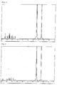
    • FIG. 1 is a 1H-NMR chart of the compound of Example 1 of the present invention (Compound 3).
    • FIG. 2 is a 1H-NMR chart of the compound of Example 2 of the present invention (Compound 4).
    • FIG. 3 is a 1H-NMR chart of the compound of Example 3 of the present invention (Compound 11).
    • FIG. 4 is a 1H-NMR chart of the compound of Example 4 of the present invention (Compound 12).
    • FIG. 5 is a diagram representing the configuration of the EL devices of Examples 8 to 11 and Comparative Examples 1 to 5.
    Mode for Carrying Out the Invention
  • The compounds having a substituted bipyridyl and triphenylene ring structure of the present invention are novel compounds, and may be synthesized by using, for example, the following method. First, the dihalide of a corresponding triphenylene compound is boronated with a compound such as bis(pinacolato)diboron to synthesize a corresponding borate product (refer to Non-Patent Document 5, for example), and this corresponding borate product is reacted with a halogenobipyridine having various substituents in a cross-coupling reaction such as Suzuki coupling (refer to Non-Patent Document 6, for example) to synthesize the compound having a substituted bipyridyl and triphenylene ring structure.
  • The compounds having a substituted bipyridyl and triphenylene ring structure also can be synthesized as follows. First, a halogenobipyridine having various substituents is boronated with a compound such as bis (pinacolato) diboron, and the resulting bipyridine borate product with various substituents is then reacted with the dihalide of a corresponding triphenylene compound in a cross-coupling reaction such as Suzuki coupling.
  • The following presents specific examples of preferred compounds among the compounds of general formulae (1) to (1''''), general formula (2), or general formula (2') having a substituted bipyridyl and triphenylene ring structure. The present invention, however, is not limited to these compounds.
    Figure imgb0008
    Figure imgb0009
    Figure imgb0010
    Figure imgb0011
    Figure imgb0012
    Figure imgb0013
    Figure imgb0014
    Figure imgb0015
    Figure imgb0016
    Figure imgb0017
    Figure imgb0018
    Figure imgb0019
    Figure imgb0020
    Figure imgb0021
    Figure imgb0022
    Figure imgb0023
    Figure imgb0024
    Figure imgb0025
    Figure imgb0026
    Figure imgb0027
    Figure imgb0028
    Figure imgb0029
    Figure imgb0030
    Figure imgb0031
    Figure imgb0032
    Figure imgb0033
    Figure imgb0034
    Figure imgb0035
    Figure imgb0036
    Figure imgb0037
    Figure imgb0038
    Figure imgb0039
    Figure imgb0040
    Figure imgb0041
    Figure imgb0042
    Figure imgb0043
    Figure imgb0044
    Figure imgb0045
    Figure imgb0046
    Figure imgb0047
    Figure imgb0048
    Figure imgb0049
    Figure imgb0050
    Figure imgb0051
    Figure imgb0052
    Figure imgb0053
    Figure imgb0054
    Figure imgb0055
    Figure imgb0056
    Figure imgb0057
    Figure imgb0058
    Figure imgb0059
    Figure imgb0060
    Figure imgb0061
    Figure imgb0062
    Figure imgb0063
    Figure imgb0064
    Figure imgb0065
    Figure imgb0066
    Figure imgb0067
    Figure imgb0068
    Figure imgb0069
    Figure imgb0070
    Figure imgb0071
    Figure imgb0072
    Figure imgb0073
    Figure imgb0074
    Figure imgb0075
  • These compounds were purified by methods such as column chromatography, adsorption using, for example, a silica gel, activated carbon, or activated clay, and recrystallization or crystallization using a solvent. The compounds were identified by using methods such as NMR analysis, mass spectrometry, and elementary analysis. Melting point, glass transition point (Tg), and work function were taken for the measurement of physical properties. Melting point can be used as an index of ease of vapor deposition, glass transition point (Tg) as an index of stability in the thin-film state, and the work function as an index of hole blocking capability.
  • The melting point and the glass transition point (Tg) were measured using a powder, using a high-sensitive differential scanning calorimeter DSC3100S (Bruker AXS).
  • For the measurement of work function, a 100 nm-thick thin film was fabricated on an ITO substrate, and an atmosphere photoelectron spectrometer (AC-3; Riken Keiki Co., Ltd.) was used.
  • The organic EL device of the present invention may have a structure including an anode, a hole transport layer, a light emitting layer, a hole blocking layer, an electron transport layer, and a cathode successively formed on a substrate, optionally with a hole injection layer between the anode and the hole transport layer, an electron injection layer between the electron transport layer and the cathode, or an electron blocking layer between the light emitting layer and the hole transport layer. Some of the organic layers in this multilayer structure may be omitted. For example, the organic EL device may be configured to include an anode, a hole transport layer, a light emitting layer, an electron transport layer, and a cathode successively formed on a substrate.
  • Each of the light emitting layer, the hole transport layer, and the electron transport layer may have a laminate structure of two or more layers.
  • Electrode materials with a large work function, such as ITO and gold, are used as the anode of the organic EL device of the present invention. The hole injection layer of the organic EL device of the present invention may be made of various materials, including, for example, porphyrin compounds as represented by copper phthalocyanine, starburst-type triphenylamine derivatives, triphenylamine trimers and tetramers such as an arylamine compound of a structure in which three or more triphenylamine structures are joined to each other within the molecule via a single bond or a divalent group that does not contain a heteroatom, accepting heterocyclic compounds such as hexacyano azatriphenylene, and coating- type polymer materials. These materials may be formed into a thin film by using a vapor deposition method, or other known methods such as spin coating and an inkjet method.
  • Examples of the material used for the hole transport layer of the organic EL device of the present invention include benzidine derivatives [such as N,N'-diphenyl-N,N'-di (m-tolyl)-benzidine (hereinafter, referred to simply as "TPD"), N,N'-diphenyl-N,N'-di(α-naphthyl)-benzidine (hereinafter, referred to simply as "NPD"), and N,N,N',N'-tetrabiphenylylbenzidine], 1,1-bis[(di-4-tolylamino)phenyl]cyclohexane (hereinafter, referred to simply as "TAPC"), various triphenylamine trimers and tetramers, and carbazole derivatives. These may be deposited alone, or may be used as a single layer deposited as a mixture with other materials, or as a laminate of individually deposited layers, a laminate of layers deposited as a mixture, or a laminate of a layer deposited alone and a layer deposited as a mixture. Examples of the material used for the hole injection/transport layer include coating-type polymer materials such as poly(3,4-ethylenedioxythiophene) (hereinafter, simply "PEDOT")/poly(styrene sulfonate) (hereinafter, simply "PSS"). These materials may be formed into a thin-film by using a vapor deposition method, or other known methods such as spin coating and an inkjet method.
  • Further, the hole injection layer or the hole transport layer may be one obtained by the P-doping of material such as trisbromophenylamine hexachloroantimony in the material commonly used for these layers. Further, for example, polymer compounds having a TPD structure as a part of the compound structure also may be used.
  • Examples of the material used for the electron blocking layer of the organic EL device of the present invention include compounds having an electron blocking effect, including, for example, carbazole derivatives such as 4,4',4''-tri(N-carbazolyl)triphenylamine (hereinafter, simply "TCTA"), 9,9-bis[4-(carbazol-9-yl)phenyl]fluorene, 1,3-bis(carbazol-9-yl)benzene (hereinafter, simply "mCP"), and 2,2-bis(4-carbazol-9-ylphenyl)adamantane (hereinafter, simply "Ad-Cz"); and compounds having a triphenylsilyl group and a triarylamine structure, as represented by 9-[4-(carbazol-9-yl)phenyl]-9-[4-(triphenylsilyl)phenyl]-9 H-fluorene. These may be deposited alone, or may be used as a single layer deposited as a mixture with other materials, or as a laminate of individually deposited layers, a laminate of a layer deposited as a mixture, or a laminate of a layer deposited alone and a layer deposited as a mixture. These materials may be formed into a thin-film by using a vapor deposition method, or other known methods such as spin coating and an inkjet method.
  • Examples of the material used for the light emitting layer of the organic EL device of the present invention include quinolinol derivative metal complexes such as Alq3, various metal complexes, anthracene derivatives, bis(styryl)benzene derivatives, pyrene derivatives, oxazole derivatives, and polyparaphenylene vinylene derivatives, in addition to the compounds having a substituted bipyridyl and triphenylene ring structure of the present invention. Further, the light emitting layer may be configured from a host material and a dopant material. Examples of the host material include thiazole derivatives, benzimidazole derivatives, and polydialkyl fluorene derivatives, in addition to the foregoing light-emitting materials. Examples of the dopant material include quinacridone, coumalin, rubrene, perylene, derivatives thereof, benzopyran derivatives, rhodamine derivatives, and aminostyryl derivatives. These may be deposited alone, or may be used as a single layer deposited as a mixture with other materials, or as a laminate of individually deposited layers, a laminate of layers deposited as a mixture, or a laminate of a layer deposited alone and a layer deposited as a mixture.
  • Further, the light-emitting material may be phosphorescent light-emitting material. Phosphorescent materials as metal complexes of metals such as iridium and platinum may be used as the phosphorescent light-emitting material. Examples of the phosphorescent materials include green phosphorescent materials such as Ir(ppy)3, blue phosphorescent materials such as FIrpic and FIr6, and red phosphorescent materials such as Btp2Ir(acac). Here, carbazole derivatives such as 4,4'-di(N-carbazolyl)biphenyl (hereinafter, simply "CBP"), TCTA, and mCP may be used as the hole injecting and transporting host material. Compounds such as p-bis (triphenylsilyl) benzene (hereinafter, simply "UGH2"), and 2,2',2"-(1,3,5-phenylene)-tris(1-phenyl-1H-benzimidazole) (hereinafter, simply "TPBI") may be used as the electron transporting host material.
  • In order to avoid concentration quenching, the doping of the phosphorescent light-emitting material in the host material should preferably be made by co-evaporation in a range of 1 to 30 weight percent with respect to the whole light emitting layer.
  • These materials may be formed into a thin-film by using a vapor deposition method, or other known methods such as spin coating and an inkjet method.
  • The hole blocking layer of the organic EL device of the present invention may be formed by using hole blocking compounds such as various rare earth complexes, oxazole derivatives, triazole derivatives, and triazine derivatives, in addition to the compounds having a substituted bipyridyl and triphenylene ring structure of present invention, and metal complexes of phenanthroline derivatives such as bathocuproin (hereinafter, simply "BCP"), and metal complexes of quinolinol derivatives such as BAlq. These materials may also serve as the material of the electron transport layer. These may be deposited alone, or may be used as a single layer deposited as a mixture with other materials, or as a laminate of individually deposited layers, a laminate of layers deposited as a mixture, or a laminate of a layer deposited alone and a layer deposited as a mixture. These materials may be formed into a thin-film by using a vapor deposition method, or other known methods such as spin coating and an inkjet method.
  • Examples of the material used for the electron transport layer of the organic EL device of the present invention include various metal complexes, triazole derivatives, triazine derivatives, oxadiazole derivatives, thiadiazole derivatives, carbodiimide derivatives, quinoxaline derivatives, phenanthroline derivatives, and silole derivatives, in addition to the compounds having a substituted bipyridyl and triphenylene ring structure of the present invention, and quinolinol derivative metal complexes such as Alq3 and BAlq. These may be deposited alone, or may be used as a single layer deposited as a mixture with other materials, or as a laminate of individually deposited layers, a laminate of layers deposited as a mixture, or a laminate of a layer deposited alone and a layer deposited as a mixture. These materials may be formed into a thin-film by using a vapor deposition method, or other known methods such as spin coating and an inkjet method.
  • Examples of the material used for the electron injection layer of the organic EL device of the present invention include alkali metal salts (such as lithium fluoride, and cesium fluoride), alkaline earth metal salts (such as magnesium fluoride), and metal oxides (such as aluminum oxide), in addition to the compounds having a substituted bipyridyl and triphenylene ring structure of the present invention. However, the electron injection layer may be omitted upon preferably selecting the electron transport layer and the cathode.
  • The electron injection layer or the electron transport layer may be one obtained by the N-doping of metals such as cesium in the materials commonly used for these layers.
  • The cathode of the organic EL device of the present invention may be made of an electrode material having a low work function (such as aluminum), or an alloy of an electrode material having an even lower work function (such as a magnesium-silver alloy, a magnesium-indium alloy, or an aluminum-magnesium alloy).
  • The following describes an embodiment of the present invention in more detail based on Examples. The present invention, however, is not limited to the following Examples.
  • Example 1 <Synthesis of 2,7-bis(2,2'-bipyridin-5-yl)triphenylene (compound 3)>
  • 2,5-Dibromopyridine (19.5 g), 2-pyridylzinc bromide (150 ml), tetrahydrofuran (90 ml), and tetrakis (triphenylphosphine) palladium (0) (4.33 g) were added to a nitrogen-substituted reaction vessel. After being cooled, the mixture was stirred at 0°C for 2 hours, and then at room temperature for 3 hours. The reaction mixture was added to a 10% disodium dihydrogen ethylenediamine tetraacetate aqueous solution, and stirred for 6 hours. The organic layer was collected by separation after adding chloroform (300 ml) . The organic layer was dried over anhydrous magnesium sulfate, and concentrated to obtain a crude product. The crude product was purified by column chromatography (support: silica gel, eluent: toluene) to obtain a white powder of 5-bromo-2,2'-bipyridine (11.1 g; yield 63%).
  • Separately, 1,2-diiodobenzene (24.4 g), 3-trimethylsilylphenylboronic acid (30 g), sodium hydroxide (8.8 g), tetrakis(triphenylphosphine)palladium(0) (4.3 g), diethylene glycol dimethyl ether (160 ml), and water (40 ml) were added to a nitrogen-substituted reaction vessel. The mixture was heated, and stirred at 95°C for 15 hours. After cooling the mixture to room temperature, water (100 ml) was added, and the organic layer was collected by separation. The organic layer was washed two times with water (100 ml), dried over anhydrous magnesium sulfate, and concentrated to obtain a crude product. The crude product was purified by column chromatography (support: silica gel, eluent: n-hexane) to obtain a white powder of 3,3"-bis(trimethylsilyl)-1,1':2',1"-terphenyl (23.3 g; yield 84%).
  • The 3,3"-bis(trimethylsilyl)-1,1':2',1"-terphenyl (23 g), bromine (12.6 ml), and chloroform (180 ml) were added to a nitrogen-substituted reaction vessel. The mixture was cooled, and stirred at -5°C for 3 hours, and then at room temperature for 4 hours. The organic layer was collected by separation after adding a saturated sodium sulfite aqueous solution (90 ml). The organic layer was then washed two times with water (100 ml), dried over anhydrous magnesium sulfate, and concentrated to obtain a crude product. The crude product was purified by recrystallization with ethanol, and washed with methanol to obtain a white powder of 3,3"-dibromo-1,1':2',1"-terphenyl (15.4 g; yield 65%).
  • The 3,3"-dibromo-1,1':2',1"-terphenyl (12.0 g), molybdenum chloride(V) (16.9 g), and dichloromethane (20 ml) were added to a nitrogen-substituted reaction vessel, and stirred at room temperature for 19 hours. After adding water (100 ml), the reaction mixture was stirred for 30 minutes, and the precipitate was collected by filtration, and washed with methanol to obtain a crude product. After adding chloroform (200 ml), n-hexane (600 ml), and silica gel (36.6 g), the crude product was purified by adsorption, and washed with chloroform to obtain a pale yellow powder of 2, 7-dibromotriphenylene (5.5 g; yield 46%).
  • The 2,7-dibromotriphenylene (5.5 g), bis(pinacolato)diboron (7.9 g), potassium acetate (4.2 g), 1,4-dioxane (50 ml) predried with a 4A molecular sieve, and a [1,1'-bis(diphenylphosphino)ferrocene]palladium(II)dichlor ide-dichloromethane complex (1:1; 0.4 g) were added to a nitrogen-substituted reaction vessel. The mixture was heated, and stirred at 80°C for 10 hours. Chloroform (150 ml) was added after cooling the mixture to 50°C, and the mixture was stirred for 30 minutes. The insoluble matter was removed by filtration, and the filtrate was concentrated to obtain a crude product. The crude product was purified by column chromatography [support: silica gel, eluent: ethyl acetate/n-hexane = 1/5 (v/v)] to obtain a white powder of 2,7-bis(4,4,5,5-tetramethyl-[1,3,2]dioxabororan-2-yl)triph enylene (4.8 g; yield 70%).
  • The 2,7-bis(4,4,5,5-tetramethyl-[1,3,2]dioxabororan-2-yl)triph enylene (2.4 g), the 5-bromo-2,2'-bipyridine (2.5 g), a 2 M potassium carbonate aqueous solution (7.7 ml), tetrakis(triphenylphosphine)palladium(0) (0.3 g), toluene (40 ml), and ethanol (10 ml) were added to a nitrogen-substituted reaction vessel. The mixture was heated, and refluxed for 9 hours while being stirred. After cooling the mixture to room temperature, the precipitate was collected by filtration. The precipitate was dissolved in chloroform (2, 000 ml), and purified by adsorption with a silica gel (11.5 g). The product was recrystallized from 1,2-dichlorobenzene to obtain a yellow powder of 2,7-bis(2,2'-bipyridin-5-yl)triphenylene (compound 3; 1.6 g; yield 60%).
  • The structure of the product yellow powder was identified by NMR. The 1H-NMR measurement result is shown in FIG. 1.
  • 1H-NMR (DMSO-d6) detected 24 hydrogen signals, as follows. δ (ppm) = 9.28(2H), 9.15(2H), 9.02-9.03(2H), 8.93-8.96(2H), 8.72(2H), 8.47-8.56(6H), 8.14-8.16(2H), 7.94-7.98(2H), 7.78-7.79(2H), 7.43-7.46(2H).
  • Example 2 <Synthesis of 2,7-bis(2,2'-bipyridin-6-yl)triphenylene (compound 4)>
  • 2,6-Dibromopyridine (19.5 g), 2-pyridylzinc bromide (150 ml), tetrahydrofuran (90 ml), and tetrakis(triphenylphosphine)palladium(0) (4.33 g) were added to a nitrogen-substituted reaction vessel. The mixture was cooled, and stirred at 0°C for 2 hours, and then at room temperature for 3 hours. The reaction mixture was added to a 10% disodium dihydrogen ethylenediamine tetraacetate aqueous solution, and stirred for 6 hours. The organic layer was collected by separation after adding chloroform (300 ml) . The organic layer was dried over anhydrous magnesium sulfate, and concentrated to obtain a crude product. The crude product was purified by column chromatography (support: silica gel, eluent: toluene) to obtain a white powder of 6-bromo-2,2'-bipyridine (11.1 g; yield 63%).
  • The 6-bromo-2,2'-bipyridine (2.4 g), the 2,7-bis(4,4,5,5-tetramethyl-[1,3,2]dioxabororan-2-yl)triph enylene (2.3 g) synthesized in Example 1, a 2 M potassium carbonate aqueous solution (7.4 ml), tetrakis(triphenylphosphine)palladium(0) (0.3 g), toluene (40 ml), and ethanol (10 ml) were added to a nitrogen-substituted reaction vessel. The mixture was heated, and refluxed for 9 hours while being stirred. After cooling the mixture to room temperature, the precipitate was collected by filtration. The insoluble matter was removed by filtration with chloroform (1,300 ml), and the product was purified by recrystallization with 1,2-dichlorobenzene to obtain a pale yellowish white powder of 2,7-bis(2,2'-bipyridin-6-yl)triphenylene (compound 4; 1.7 g; yield 66%).
  • The structure of the product pale yellowish white powder was identified by NMR. The 1H-NMR measurement result is shown in FIG. 2.
    1H-NMR (DMSO-d6) detected 24 hydrogen signals, as follows. δ (ppm) = 9.50(2H), 8.92-8.98(4H), 8.64-8.70(4H), 8.54-8.57(2H), 8.38-8.40(2H), 8.28-8.30(2H), 8.06-8.10(2H), 7.98-8.01(2H), 7.78-7.80(2H), 7.43-7.45(2H).
  • Example 3 <Synthesis of 2,11-bis(2,2'-bipyridin-5-yl)triphenylene (compound 11)>
  • 1,2-Dibromobenzene (10 g), bis(pinacolato)diboron (23.7 g), potassium acetate (12.5 g), 1,4-dioxane (150 ml) predried with a 4A molecular sieve, and a [1,1'-bis(diphenylphosphino)ferrocene]palladium(II)dichlor ide-dichloromethane complex (1:1; 1.0 g) were added to a nitrogen-substituted reaction vessel. The mixture was heated, and stirred at 80°C for 10 hours. Chloroform (150 ml) was added after cooling the mixture to 50°C, and the mixture was stirred for 30 minutes. The insoluble matter was removed by filtration, and the filtrate was concentrated to obtain a crude product. The crude product was purified by column chromatography [support: silica gel, eluent: ethyl acetate/n-hexane = 1/4 (v/v)] to obtain a white powder of 1,2-bis(4,4,5,5-tetramethyl-[1,3,2]dioxabororan-2-yl)benze ne (7.2 g; yield 54%).
  • Separately, 3,3'-dimethoxy-1,1'-biphenyl (30 g), bromine (15.8 ml), and acetic acid (250 ml) were added to a nitrogen-substituted reaction vessel, and the mixture was stirred at room temperature for 2 hours. After adding a saturated sodium sulfite aqueous solution (90 ml) to the reaction mixture, the organic layer was collected by separation with chloroform (200 ml). The organic layer was washed two times with water (100 ml), dried over anhydrous magnesium sulfate, and concentrated to obtain a crude product. The crude product was washed with ethanol to obtain a white powder of 2,2'-dibromo-3,3'-dimethoxy-1,1'-biphenyl (36.3 g; yield 70%).
  • The 2,2'-dibromo-3,3'-dimethoxy-1,1'-biphenyl (2.8 g), the 1,2-bis(4,4,5,5-tetrame.thyl-[1,3,2]dioxabororan-2-yl)benze ne (3.0 g), potassium phosphate (9.6 g), tetrakis(triphenylphosphine)palladium(0) (0.43 g), tetrahydrofuran (50 ml), and water (15 ml) were added to a nitrogen-substituted reaction vessel. The mixture was heated, and stirred at 60°C for 48 hours. After cooling the mixture to room temperature, the organic layer was collected by separation after adding chloroform (100 ml). The organic layer was washed two times with water (50 ml), dried over anhydrous magnesium sulfate, and concentrated to obtain a crude product. The crude product was purified by column chromatography [support: silica gel, eluent: ethyl acetate/n-hexane/methylene chloride = 1/10/1 (v/v/v)], and washed with methanol to obtain a white powder of 2,11-dimethoxytriphenylene (1.72 g; 65.6%).
  • The 2,11-dimethoxytriphenylene (1.5 g), a boron tribromide:dichloromethane solution (1 mol/L; 10.9 ml), and dichloromethane (50 ml) were added to a nitrogen-substituted reaction vessel cooled to -78°C. The mixture was heated to room temperature, and stirred for 20 hours. After adding water (50 ml) to the reaction mixture, the mixture was stirred for 30 minutes, and the precipitate was collected by filtration. The precipitate was washed with methanol to obtain a white powder of triphenylene-2,11-diol (1.25 g; yield 93%).
  • The triphenylene-2,11-diol (1.25 g), N-phenyl-bis(trifluoromethanesulfoneimide) (6.87 g), sodium carbonate (5.1 g), and dimethylformamide (50 ml) were added to a nitrogen-substituted reaction vessel, and the mixture was stirred at room temperature for 12 hours. After adding water (50 ml) to the reaction mixture, the mixture was stirred for 30 minutes, and the precipitate was collected by filtration. The precipitate was washed with methanol to obtain a white powder of triphenylene-2,11-diyl-bis(trifluoromethanesulfonate) (2.38 g; yield 91%).
  • The triphenylene-2,11-diyl-bis(trifluoromethanesulfonate) (2.3 g), bis (pinacolato) diboron (2.5 g), potassium acetate (1.3 g), 1,4-dioxane (50 ml) predried with a 4A molecular sieve, and a [1,1'-bis(diphenylphosphino)ferrocene]palladium(II)dichlor ide-dichloromethane complex (1:1; 0.1 g) were added to a nitrogen-substituted reaction vessel. The mixture was heated, and stirred at 80°C for 10 hours. Chloroform (150 ml) was added after cooling the mixture to 50°C, and the mixture was stirred for 30 minutes. The insoluble matter was removed by filtration, and the filtrate was concentrated to obtain a crude product. The crude product was purified by column chromatography [support: silica gel, eluent: ethyl acetate/n-hexane = 1/5 (v/v)] to obtain a white powder of 2,11-bis(4,4,5,5-tetramethyl-[1,3,2]dioxabororan-2-yl)trip henylene (1.1 g; yield 52%).
  • The 2,11-bis(4,4,5,5-tetramethyl-[1,3,2]dioxabororan-2-yl)trip henylene (0.9 g), the 5-bromo-2,2'-bipyridine (0.9 g) synthesized in Example 1, a 2 M potassium carbonate aqueous solution (2.9 ml), tetrakis(triphenylphosphine)palladium(0) (0.1 g), toluene (40 ml), and ethanol (10 ml) were added to a nitrogen-substituted reaction vessel. The mixture was heated, and refluxed for 9 hours while being stirred. After cooling the mixture to room temperature, the precipitate was collected by filtration. The precipitate was dissolved in chloroform (1,000 ml), and purified by adsorption with a silica gel (11.5 g). The product was then recrystallized from 1,2-dichlorobenzene to obtain a yellow powder of 2,11-bis(2,2'-bipyridin-5-yl)triphenylene (compound 11; 0.7 g; yield 70%).
  • The structure of the product yellow powder was identified by NMR. The 1H-NMR measurement result is shown in FIG. 3.
    1H-NMR (DMSO-d6) detected 24 hydrogen signals, as follows. δ (ppm) = 9.41(2H), 9.37(2H), 9.95(2H), 8.88-8.85(2H), 8.71(2H), 8.60-8.57(2H), 8.56-8.54(2H), 8.52-8.45(2H), 8.16(2H), 7.95-7.98(2H), 7.74(2H), 7.45(2H).
  • Example 4 <Synthesis of 2,11-bis(2,2'-bipyridin-6-yl)triphenylene (compound 12)>
  • The 2,11-bis(4,4,5,5-tetramethyl-[1,3,2]dioxabororan-2-yl)trip henylene (0.8 g) synthesized in Example 3, the 6-bromo-2,2'-bipyridine (0.8 g) synthesized in Example 2, a 2 M potassium carbonate aqueous solution (2.3 ml), tetrakis(triphenylphosphine)palladium(0) (0.1 g), toluene (40 ml), and ethanol (10 ml) were added to a nitrogen-substituted reaction vessel. The mixture was heated, and refluxed for 9 hours while being stirred. After cooling the mixture to room temperature, the precipitate was collected by filtration. Chloroform (1,300 ml) was added to the precipitate, and the insoluble matter was removed by filtration. The product was then purified by recrystallization with 1,2-dichlorobenzene to obtain a pale yellowish white powder of 2,11-bis(2,2'-bipyridin-6-yl)triphenylene (compound 12; 0.6 g; yield 71%).
  • The structure of the product pale yellowish white powder was identified by NMR. The 1H-NMR measurement result is shown in FIG. 4.
    1H-NMR (DMSO-d6) detected 24 hydrogen signals, as follows. δ (ppm) = 9.74(2H), 8.98(2H), 8.90-8.87(2H), 8.70(2H), 8.66-8.62(4H), 8.48(2H), 8.41(2H), 8.17-8.13(2H), 7.79-7.75(4H), 7.43-7.40(2H).
  • Example 5 <Synthesis of 2,7-di([2,4'-bipyridin]-5-yl)triphenylene (compound 55) >
  • 2,5-Dibromopyridine (9.6 g), 4-pyridineboronic acid (2.5 g), toluene (50 ml), ethanol (40 ml), a 2 M potassium carbonate aqueous solution (15.2 ml), and tetrakis(triphenylphosphine)palladium(0) (1.50 g) were added to a nitrogen-substituted reaction vessel. The mixture was heated, and refluxed for 24 hours while being stirred. After cooling the mixture to room temperature, chloroform (500 ml) and water (300 ml) were added, and the organic layer was collected by separation. The organic layer was washed two times with water (100 ml), dried over anhydrous magnesium sulfate, and concentrated to obtain a crude product. The crude product was purified by column chromatography [support: silica gel, eluent: toluene:ethyl acetate = 1:1 (v/v)] to obtain a white powder of 5-bromo-2,4'-bipyridine (3.3 g; yield 69%).
  • The 5-bromo-2,4'-bipyridine (2.4 g), the 2,7-bis(4,4,5,5-tetramethyl-[1,3,2]dioxabororan-2-yl)triph enylene (2.0 g) synthesized in Example 1, a 2 M potassium carbonate aqueous solution (6.3 ml), tetrakis(triphenylphosphine)palladium(0) (0.3 g), toluene (40 ml), and ethanol (25 ml) were added to a nitrogen-substituted reaction vessel. The mixture was heated, and refluxed for 24 hours while being stirred. After cooling the mixture to room temperature, the precipitate was collected by filtration. Chloroform (1,300 ml) was added to the precipitate, and the insoluble matter was removed by filtration. The product was then purified by recrystallization with 1,2-dichlorobenzene to obtain a pale yellowish white powder of 2,7-di([2,4'-bipyridin]-5-yl)triphenylene (compound 55; 1.1 g; yield 50%).
  • The structure of the pale yellowish white powder was identified by using a matrix-assisted laser desorption/ionization time-of-flight mass spectrometer (AXIMA-CFR Plus; Shimadzu Corporation), and an elementary analysis device (Yanaco CHNCORDER MT-5; Yanamoto Seisakusho).
    MS (m/z) 537 [calculated value (m/z) 536.20], elementary analysis, measured value: C;85.08, H;4.42, N;10.39, calculated value (C38H24N4): C;85.05, H;4.51, N;10.44.
  • Comparative Synthesis Example 1 <Synthesis of 3,3"-bis(2,2'-bipyridin-5-yl)-1,1':2',1"-terphenyl (comparative compound 1)>
  • The 3,3"-dibromo-1,1':2',1"-terphenyl (5.0 g) synthesized in Example 1, bis(pinacolato)diboron (6.9 g), potassium acetate (3.8 g), 1,4-dioxane (50 ml) predried with a 4A molecular sieve, and a [1,1'-bis(diphenylphosphino)ferrocene]palladium(II)dichlor ide-dichloromethane complex (1:1; 0.3 g) were added to a nitrogen-substituted reaction vessel. The mixture was heated, and stirred at 80°C for 11 hours. Chloroform (100 ml) was added after cooling the mixture to 50°C, and the mixture was stirred for 30 minutes. The insoluble matter was removed by filtration, and the filtrate was concentrated to obtain a crude product. The crude product was purified by column chromatography [support: silica gel, eluent: ethyl acetate/n-hexane = 1/20 (v/v) to obtain a white powder of 3,3"-bis(4,4,5,5-tetramethyl-[1,3,2]dioxabororan-2-yl)-1, 1':2',1"-terphenyl (3.8 g; yield 61%).
  • The 3,3"-bis(4,4,5,5-tetramethyl-[1,3,2]dioxabororan-2-yl)-1, 1':2',1"-terphenyl (1.8 g), the 5-bromo-2,2'-bipyridine (1.8 g) synthesized in Example 1, a 2 M potassium carbonate aqueous solution (5.8 ml), tetrakis(triphenylphosphine)palladium(0) (0.2 g), toluene (40 ml), and ethanol (10 ml) were added to a nitrogen-substituted reaction vessel. The mixture was heated, and refluxed for 20 hours while being stirred. After cooling the mixture to room temperature, water (30 ml) and chloroform (100 ml) were added, and the organic layer was collected by separation. The organic layer was washed with water (100 ml), dried over anhydrous magnesium sulfate, and concentrated to obtain a crude product. The crude product was purified by column chromatography [support: NH silica gel, eluent: ethyl acetate/n-hexane = 1/5 (v/v)] to obtain a white powder of 3,3"-bis(2,2'-bipyridin-5-yl)-1,1':2',1"-terphenyl represented by the following structural formula (comparative compound 1; 1.5 g; yield 80%).
    Figure imgb0076
  • The structure of the product white powder was identified by NMR.
    1H-NMR (CDCl3) detected 26 hydrogen signals, as follows. δ (ppm) = 8.65-8.66(2H), 8.51-8.53(2H), 8.31-8.33(2H), 8.08(2H), 7.99-8.01(2H), 7.71-7.79(4H), 7.59-7.61(2H), 7.54-7.56(2H), 7.50-7.52(2H), 7.34-7.38(2H), 7.25-7.28 (4H) .
  • Comparative Synthesis Example 2 <Synthesis of 3,3"-bis(2,2'-bipyridin-6-yl)-1,1':2',1"-terphenyl (comparative compound 2)>
  • The 3,3"-bis(4,4,5,5-tetramethyl-[1,3,2]dioxabororan-2-yl)-1, 1':2',1"-terphenyl (1.8 g) synthesized in Comparative Synthesis Example 1, the 6-bromo-2,2'-bipyridine (1.8 g) synthesized in Example 2, a 2 M potassium carbonate aqueous solution (5.8 ml), tetrakis(triphenylphosphine)palladium(0) (0.2 g), toluene (40 ml), and ethanol (10 ml) were added to a nitrogen-substituted reaction vessel. The mixture was heated, and refluxed for 8 hours while being stirred. After cooling the mixture to room temperature, water (30 ml) and toluene (40 ml) were added, and the organic layer was collected by separation. The organic layer was washed with water (30 ml), dried over anhydrous magnesium sulfate, and concentrated to obtain a crude product. The crude product was purified by column chromatography [support: NH silica gel, eluent: ethyl acetate/n-hexane = 1/5 (v/v)] to obtain a white powder of 3,3"-bis(2,2'-bipyridin-6-yl)-1,1':2',1"-terphenyl represented by the following structural formula (comparative compound 2; 1.5 g; yield 75%).
    Figure imgb0077
  • The structure of the product white powder was identified by NMR.
    1H-NMR (CDCl3) detected 26 hydrogen signals, as follows. δ (ppm) = 8.66-8.68(4H), 8.35-8.40(4H), 7.79-7.83(2H), 7.69-7.72(2H), 7.45-7.58(8H), 7.35-7.39(4H), 7.28-7.31(2H).
  • Comparative Synthesis Example 3 <Synthesis of 4,4"-bis(2,2'-bipyridin-6-yl)-1,1':2',1"-terphenyl (comparative compound 3)>
  • 1,2-Diiodobenzene (20 g), 4-trimethylsilylphenylboronic acid (25 g), sodium hydroxide (7.4 g), tetrakis(triphenylphosphine)palladium(0) (3.6 g), diethylene glycol dimethyl ether (240 ml), and water (60 ml) were added to a nitrogen-substituted reaction vessel. The mixture was heated, and stirred at 95°C for 15 hours. Water (100 ml) was added after cooling the mixture to room temperature, and the organic layer was collected by separation. The organic layer was washed two times with water (100 ml), dried over anhydrous magnesium sulfate, and concentrated to obtain a crude product. The crude product was purified by column chromatography (support: silica gel, eluent: n-hexane) to obtain a white powder of 4,4"-bis(trimethylsilyl)-1,1':2',1"-terphenyl (21.1 g; yield 93%).
  • The 4,4"-bis(trimethylsilyl)-1,1':2',1"-terphenyl (21 g), bromine (11.5 ml), and chloroform (150 ml) were added to a nitrogen-substituted reaction vessel. The mixture was cooled, and stirred at -5°C for 3 hours, and then at room temperature for 4 hours. The organic layer was collected by separation after adding a saturated sodium sulfite aqueous solution (90 ml). The organic layer was then washed two times with water (100 ml), dried over anhydrous magnesium sulfate, and concentrated to obtain a crude product. The crude product was purified by recrystallization with ethanol, and washed with methanol to obtain a white powder of 4,4"-dibromo-1,1':2',1"-terphenyl (14.9 g; yield 68%).
  • The 4,4"-dibromo-1,1':2',1"-terphenyl (5.0 g), bis(pinacolato)diboron (7.2 g), potassium acetate (3.8 g), 1,4-dioxane (50 ml) predried with a 4A molecular sieve, and a [1,1'-bis(diphenylphosphino)ferrocene]palladium(II)dichlor ide-dichloromethane complex (1:1; 0.3 g) were added to a nitrogen-substituted reaction vessel. The mixture was heated, and stirred at 80°C for 10 hours. Chloroform (150 ml) was added after cooling the mixture to 50°C, and the mixture was stirred for 30 minutes. The insoluble matter was removed by filtration, and the filtrate was concentrated to obtain a crude product. The crude product was purified by column chromatography [support: silica gel, eluent: ethyl acetate/n-hexane = 1/5 (v/v)] to obtain a white powder of 4,4"-bis(4,4,5,5-tetramethyl-[1,3,2]dioxabororan-2-yl)-1, 1':2',1"-terphenyl (3.5 g; yield 56%).
  • The 4,4"-bis(4,4,5,5-tetramethyl-[1,3,2]dioxabororan-2-yl)-1, 1':2',1"-terphenyl (2.0 g), the 6-bromo-2,2'-bipyridine (2.0 g) synthesized in Example 2, a 2 M potassium carbonate aqueous solution (6.0 ml), tetrakis(triphenylphosphine)palladium(0) (0.2 g), toluene (32 ml), and ethanol (8 ml) were added to a nitrogen-substituted reaction vessel. The mixture was heated, and refluxed for 9 hours while being stirred. Water (100 ml) was added after cooling the mixture to room temperature, and the organic layer was collected by separation. The organic layer was washed two times with water (100 ml), dried over anhydrous magnesium sulfate, and concentrated to obtain a crude product. The crude product was purified by column chromatography (support: silica gel, eluent: chloroform), and recrystallized with toluene to obtain a white powder of 4,4"-bis(2,2'-bipyridin-6-yl)-1,1':2',1"-terphenyl represented by the following structural formula (comparative compound 3; 1.6 g; yield 74%).
    Figure imgb0078
  • The structure of the product white powder was identified by NMR.
    1H-NMR (CDCl3) detected 26 hydrogen signals, as follows. δ (ppm) = 8.67(2H), 8.60(2H), 8.33(2H), 8.06(4H), 7.78-7.86(4H), 7.74(2H), 7.53-7.48(4H), 7.36(4H), 7.30-7.28(2H).
  • Example 6
  • The melting points and the glass transition points of the compounds of the present invention were determined using a high-sensitive differential scanning calorimeter (DSC 3100S; Bruker AXS).
    Melting point Glass transition point
    Compound of Example 1 of the present invention 338°C None
    Compound of Example 2 of the present invention 285°C None
  • The compounds of the present invention were not shown to have glass transition points. This indicates that the compounds of the present invention have a stable thin-film state.
  • Example 7
  • A 50 nm-thick vapor-deposited film was fabricated on an ITO substrate using the compounds of the present invention. The work function was measured using an atmosphere photoelectron spectrometer (Model AC-3 produced by Riken Keiki Co., Ltd.).
    Work function
    Compound of Example 1 of the present invention 5.74 eV
    Compound of Example 2 of the present invention 5.69 eV
    Compound of Example 3 of the present invention 5.82 eV
    Compound of Example 4 of the present invention 5.73 eV
    Compound of Example 5 of the present invention 6.21 eV
  • As shown above, the compounds of the present invention have work functions greater than the work function 5.4 eV of common hole transport materials such as NPD and TPD, and have high hole blocking capability.
  • Example 8
  • The organic EL device, as illustrated in FIG. 5, was fabricated from a hole transport layer 3, a light emitting layer 4, an electron transport layer 5, an electron injection layer 6, and a cathode (silver electrode) 7 successively formed by vapor deposition on a glass substrate 1 that had been provided beforehand with an ITO electrode as a transparent anode 2.
  • Specifically, the glass substrate 1 having ITO (thickness 100 nm) formed thereon was washed with an organic solvent, and subjected to a UV ozone treatment to wash the surface. The glass substrate with the ITO electrode was then installed, in a vacuum vapor deposition apparatus, and the pressure was reduced to 0.001 Pa or less. This was followed by formation of the hole transport layer 3 by vapor depositing NPD over the transparent anode 2 in a thickness of 50 nm at a deposition rate of 2 Å/s. The light emitting layer 4 was then formed on the hole transport layer 3 by forming Alq3 in a thickness of 20 nm at a deposition rate of 2 Å/s. Then, the electron transport layer 5 was formed on the light emitting layer 4 by forming the compound of Example 1 of the present invention (compound 3) in a thickness of 30 nm at a deposition rate of 2 Å/s. The electron injection layer 6 was then formed on the electron transport layer 5 by forming a magnesium silver alloy in a thickness of 100 nm at a deposition rate of 3.3 Å/s. Finally, the cathode 7 was formed by vapor depositing silver in a thickness of 10 nm. The characteristics of the organic EL device thus fabricated were measured in an atmosphere at ordinary temperature.
  • Table 1 summarizes the results of the emission characteristics measurements performed by applying a DC voltage to the organic EL device fabricated with the compound of Example 1 of the present invention (compound 3).
  • Example 9
  • An organic EL device was fabricated under the same conditions used in Example 8, except that the material of the electron transport layer 5 used in Example 8 was changed to the compound of Example 3 of the present invention (compound 11). The characteristics of the organic EL device thus fabricated were measured in an atmosphere at ordinary temperature. Table 1 summarizes the results of the emission characteristics measurements performed by applying a DC voltage to the organic EL device.
  • Example 10
  • An organic EL device was fabricated under the same conditions used in Example 8, except that the material of the electron transport layer 5 used in Example 8 was changed to the compound of Example 5 of the present invention (compound 55). The characteristics of the organic EL device thus fabricated were measured in an atmosphere at ordinary temperature. Table 1 summarizes the results of the emission characteristics measurements performed by applying a DC voltage to the organic EL device.
  • Comparative Example 1
  • For comparison, an organic EL device was fabricated under the same conditions used in Example 8, except that the material of the electron transport layer 5 used in Example 8 was changed to Alq3. The characteristics of the organic EL device thus fabricated were measured in an atmosphere at ordinary temperature. Table 1 summarizes the results of the emission characteristics measurements performed by applying a DC voltage to the organic EL device.
  • Comparative Example 2
  • For comparison, an organic EL device was fabricated under the same conditions used in Example 8, except that the material of the electron transport layer 5 used in Example 8 was changed to the comparative compound 1. The characteristics of the organic EL device thus fabricated were measured in an atmosphere at ordinary temperature. Table 1 summarizes the results of the emission characteristics measurements performed by applying a DC voltage to the organic EL device.
  • Comparative Example 3
  • For comparison, an organic EL device was fabricated under the same conditions used in Example 8, except that the material of the electron transport layer 5 used in Example 8 was changed to the comparative compound 2. The characteristics of the organic EL device thus fabricated were measured in an atmosphere at ordinary temperature. Table 1 summarizes the results of the emission characteristics measurements performed by applying a DC voltage to the organic EL device.
  • Comparative Example 4
  • For comparison, an organic EL device was fabricated under the same conditions used in Example 8, except that the material of the electron transport layer 5 used in Example 8 was changed to the comparative compound 3. The characteristics of the organic EL device thus fabricated were measured in an atmosphere at ordinary temperature. Table 1 summarizes the results of the emission characteristics measurements performed by applying a DC voltage to the organic EL device. Table 1
    Voltage [V] (@10mA/cm2) Luminance [cd/m2] (@10mA/cm2) Current efficiency [cd/A] (@10mA/cm2) Power efficiency [Im/W] (@10mA/cm2)
    Ex. 8 Compound 3 4.10 376 3.34 2.56
    Ex. 9 Compound 11 4.40 335 3.41 2.43
    Ex. 10 Compound 55 4.60 296 2.81 1.92
    Com. Ex. 1 Alq3 5.70 268 2.60 1.43
    Com. Ex. 2 Comparative compound 1 6.60 303 2.76 1.31
    Com. Ex. 3 Comparative compound 2 7.50 263 2.63 1.10
    Com. Ex. 4 Comparative compound 3 7.40 257 2.45 1.04
  • As can be seen in Table 1, the driving voltage at the current density of 10 mA/cm2 was 4.10 V, 4.40 V, and 4.60 V in Examples 8, 9, and 10, respectively, greatly lower than 5. 70 V of Comparative Example 1 in which Alq3 was used, and 6.60 V to 7.50 V of Comparative Examples 2 to 4 in which the comparative compounds 1 to 3 were used. Further, the luminance, the current efficiency, and the power efficiency all greatly improved at the current density of 10 mA/cm2.
  • Example 11
  • The glass substrate 1 having ITO (thickness 100 nm) formed thereon was washed with an organic solvent, and subjected to a UV ozone treatment to wash the surface. The glass substrate with the ITO electrode was then installed in a vacuum vapor deposition apparatus, and the pressure was reduced to 0.001 Pa or less. This was followed by formation of the hole transport layer 3 by forming NPD over the transparent anode 2 in a thickness of 60 nm at a deposition rate of 2 Å/s. Then, the light emitting layer 4 was formed on the hole transport layer 3 in a thickness of 30 nm by the dual vapor deposition of 2-(tert-butyl)-9,10-diphenylanthracene (TBADN) and blue fluorescence emitter DPAVB at a deposition rate ratio of TBADN:DPAVB = 95:5. The electron transport layer 5 was then formed on the light emitting layer 4 by forming the compound of Example 1 of the present invention (compound 3) in a thickness of 30 nm at a deposition rate of 2 Å/s. Then, the electron injection layer 6 was formed on the electron transport layer 5 by forming a magnesium silver alloy in a thickness of 100 nm at a deposition rate of 3.3 Å/s. Finally, the cathode 7 was formed by vapor depositing silver in a thickness of 10 nm. The characteristics of the organic EL device thus fabricated were measured in an atmosphere at ordinary temperature.
  • Table 2 summarizes the results of the emission characteristics measurements performed by applying a DC voltage to the organic EL device fabricated with the compound of Example 1 of the present invention (compound 3).
  • Comparative Example 5
  • For comparison, an organic EL device was fabricated under the same conditions used in Example 11, except that the material of the electron transport layer 5 used in Example 11 was changed to Alq3. The characteristics of the organic EL device thus fabricated were measured in an atmosphere at ordinary temperature. Table 2 summarizes the results of the emission characteristics measurements performed by applying a DC voltage to the organic EL device. Table 2
    Voltage [V] (@10mA/cm2) Luminance [cd/m2] (@10mA/cm2) Current efficiency [cd/A] (@10mA/cm2) Power efficiency [Im/W] (@10mA/cm2)
    Ex. 11 Compound 3 4.80 712 6.48 4.24
    Com. Ex. 5 Alq3 8.80 772 7.68 2.74
  • As can be seen in Table 2, the driving voltage at the current density of 10 mA/cm2 was 4.80 V in Example 11, greatly lower than 8.80 V of Comparative Example 5 in which Alq3 was used. Further, the power efficiency greatly improved at the current density of 10 mA/cm2.
  • As is clear from these results, the organic EL devices using the compounds having a bipyridyl group and a triphenylene ring structure of the present invention can greatly improve power efficiency, and can achieve a considerably low actual driving voltage compared to the devices that use the common electron transport material Alq3, and the devices that use the comparative compounds 1 to 3 having a non-planar central skeleton structure.
  • As demonstrated above, the organic EL devices using the compounds having a bipyridyl group and a triphenylene ring structure of the present invention have a considerably low driving voltage. The electron mobility of the compounds having a bipyridyl group and a triphenylene ring structure of the present invention is thus expected to be much faster than that of the common electron transport material Alq3.
  • Industrial Applicability
  • The compounds having a bipyridyl group and a triphenylene ring structure of the present invention have a desirable electron injection and transport performance and a stable thin-film state, and are desirable for organic EL devices. The organic EL device produced by using the compounds can have high efficiency and a low actual driving voltage, and can thus have improved durability. There are potential applications for, for example, home electronic appliances and illuminations.
  • Description of Reference Numerals and Signs
  • 1
    Glass substrate
    2
    Transparent anode
    3
    Hole transport layer
    4
    Light emitting layer
    5
    Electron transport layer
    6
    Electron injection layer
    7
    Cathode

Claims (6)

  1. A compound of the following general formula (2) having a substituted bipyridyl and triphenylene ring structure,
    Figure imgb0079
    wherein R19 to R39 may be the same or different, and represent a hydrogen atom, a deuterium atom, a fluorine atom, a chlorine atom, cyano, trifluoromethyl, linear or branched alkyl of 1 to 6 carbon atoms that may have a substituent, a substituted or unsubstituted aromatic hydrocarbon group, a substituted or unsubstituted aromatic heterocyclic group, or a substituted or unsubstituted condensed polycyclic aromatic group, and wherein n3, n4, and n5 may be the same or different, and represent 2 or 3, and the plurality of R22 to R30 may be the same or different.
  2. The compound having a substituted bipyridyl and triphenylene ring structure according to claim 1, wherein the compound is represented by the following general formula (2'),
    Figure imgb0080
    wherein R19 to R39 may be the same or different, and represent a hydrogen atom, a deuterium atom, a fluorine atom, a chlorine atom, cyano, trifluoromethyl, linear or branched alkyl of 1 to 6 carbon atoms that may have a substituent, a substituted or unsubstituted aromatic hydrocarbon group, a substituted or unsubstituted aromatic heterocyclic group, or a substituted or unsubstituted condensed polycyclic aromatic group, and wherein n3, n4, and n5 may be the same or different, and represent 2 or 3, and the plurality of R22 to R30 may be the same or different, respectively.
  3. An organic electroluminescent device comprising a pair of electrodes, and one or more organic layers sandwiched between the pair of electrodes, wherein a compound of the following general formula (2) having a substituted bipyridyl and triphenylene ring structure is used as constituent material of at least one of the organic layers,
    Figure imgb0081
    wherein R19 to R39 may be the same or different, and represent a hydrogen atom, a deuterium atom, a fluorine atom, a chlorine atom, cyano, trifluoromethyl, linear or branched alkyl of 1 to 6 carbon atoms that may have a substituent, a substituted or unsubstituted aromatic hydrocarbon group, a substituted or unsubstituted aromatic heterocyclic group, or a substituted or unsubstituted condensed polycyclic aromatic group, and wherein n3, n4, and n5 may be the same or different, and represent 2 or 3, and the plurality of R22 to R30 may be the same or different, respectively.
  4. The organic electroluminescent device according to claim 3, wherein the organic layer is an electron transport layer, and the compound represented by the general formula (2) is used as at least one of constituent materials in the electron transport layer.
  5. The organic electroluminescent device according to claim 3, wherein the organic layer is an electron injection layer, and the compound represented by the general formula (2) is used as at least one of constituent materials in the electron injection layer.
  6. The organic electroluminescent device according to claim 3, wherein the organic layer is a light emitting layer, and the compound represented by the general formula (2) is used as at least one of constituent materials in the light emitting layer.
EP17001154.8A 2011-02-23 2012-02-23 Compound having substituted triphenylene ring structure, and organic electroluminescent device Withdrawn EP3255040A1 (en)

Applications Claiming Priority (2)

Application Number Priority Date Filing Date Title
JP2011037322 2011-02-23
EP12749099.3A EP2679581B1 (en) 2011-02-23 2012-02-23 Compound containing substituted triphenyle ring structure, and organic electroluminescent element

Related Parent Applications (1)

Application Number Title Priority Date Filing Date
EP12749099.3A Division EP2679581B1 (en) 2011-02-23 2012-02-23 Compound containing substituted triphenyle ring structure, and organic electroluminescent element

Publications (1)

Publication Number Publication Date
EP3255040A1 true EP3255040A1 (en) 2017-12-13

Family

ID=46720537

Family Applications (2)

Application Number Title Priority Date Filing Date
EP12749099.3A Active EP2679581B1 (en) 2011-02-23 2012-02-23 Compound containing substituted triphenyle ring structure, and organic electroluminescent element
EP17001154.8A Withdrawn EP3255040A1 (en) 2011-02-23 2012-02-23 Compound having substituted triphenylene ring structure, and organic electroluminescent device

Family Applications Before (1)

Application Number Title Priority Date Filing Date
EP12749099.3A Active EP2679581B1 (en) 2011-02-23 2012-02-23 Compound containing substituted triphenyle ring structure, and organic electroluminescent element

Country Status (7)

Country Link
US (3) US9685612B2 (en)
EP (2) EP2679581B1 (en)
JP (2) JP5453621B2 (en)
KR (1) KR101975067B1 (en)
CN (1) CN103402981A (en)
TW (1) TWI508958B (en)
WO (1) WO2012114745A1 (en)

Families Citing this family (13)

* Cited by examiner, † Cited by third party
Publication number Priority date Publication date Assignee Title
JPH1144632A (en) * 1997-07-28 1999-02-16 Toa Medical Electronics Co Ltd Method for determining abnormality in data of particle-measuring device
CN103402981A (en) * 2011-02-23 2013-11-20 保土谷化学工业株式会社 Compound containing substituted triphenyle ring structure, and organic electroluminescent element
JP6126577B2 (en) * 2012-02-28 2017-05-10 保土谷化学工業株式会社 Compound having pyridyl group having substituent and triphenylene ring structure, and organic electroluminescence device
KR20140135525A (en) 2013-05-16 2014-11-26 제일모직주식회사 Luminescent material and organic optoelectric device and display device
KR101618683B1 (en) * 2013-05-16 2016-05-09 제일모직 주식회사 Organic compound and organic optoelectric device and display device
KR101779110B1 (en) 2013-10-11 2017-09-18 제일모직 주식회사 Organic optoelectric device and display device
JP6354157B2 (en) * 2013-12-26 2018-07-11 日立化成株式会社 Charge transporting material, ink composition using the material, organic electronics element, organic electroluminescence element, display element, display device and lighting device
KR102255197B1 (en) * 2014-05-02 2021-05-25 삼성디스플레이 주식회사 Organic light emitting device
KR102245164B1 (en) * 2014-08-22 2021-04-27 엘지디스플레이 주식회사 Organic light emitting device and method of fabricating the same
KR101906065B1 (en) 2016-07-27 2018-10-10 주식회사 엘지화학 Polycyclic compound and organic light emitting device comprising the same
JP7002925B2 (en) * 2017-11-13 2022-01-20 東ソー株式会社 Organic electroluminescence device containing dinaphthotetraphenylene compound
CN109575937A (en) * 2018-12-01 2019-04-05 四川师范大学 A kind of truxene ketone-benzophenanthrene disc liquid-crystal compounds and preparation method thereof
CN112409374B (en) * 2020-11-20 2022-10-14 四川师范大学 Preparation method of rigid core direct-connected graphene-like benzophenanthrene discotic liquid crystal and mesomorphism

Citations (9)

* Cited by examiner, † Cited by third party
Publication number Priority date Publication date Assignee Title
JPH0848656A (en) 1994-02-08 1996-02-20 Tdk Corp Compound for organic el element and organic el element
JP2734341B2 (en) 1993-03-26 1998-03-30 住友電気工業株式会社 Organic electroluminescence device
JP3194657B2 (en) 1993-11-01 2001-07-30 松下電器産業株式会社 EL device
WO2003060956A2 (en) 2002-01-18 2003-07-24 Lg Chem, Ltd. New material for transporting electrons and organic electroluminescent display using the same
JP2008150365A (en) * 2006-11-20 2008-07-03 Chisso Corp Electron transport material and organic electroluminescent device using the same
JP2008214307A (en) * 2007-03-07 2008-09-18 Chisso Corp Electron transport material and organic electroluminescent element using the same
JP2008214306A (en) * 2007-03-07 2008-09-18 Chisso Corp Electron transport material and organic electroluminescent element using the same
JP2008247895A (en) * 2007-03-07 2008-10-16 Chisso Corp Electron transport material and organic electroluminescent element using the same
US20090134780A1 (en) * 2005-09-05 2009-05-28 Youhei Ono Electron transport material and organic electroluminescent device using the same

Family Cites Families (5)

* Cited by examiner, † Cited by third party
Publication number Priority date Publication date Assignee Title
JP5011743B2 (en) * 2005-02-15 2012-08-29 東ソー株式会社 Π-conjugated compound having cardo structure, and production method and use thereof
JP4843321B2 (en) * 2006-01-31 2011-12-21 Jnc株式会社 Coumarin compound, material for light emitting device, and organic electroluminescent device
JP2008156266A (en) * 2006-12-22 2008-07-10 Chisso Corp Electron transporting material and organic electroluminescent device produced by using the same
KR101551207B1 (en) * 2008-09-04 2015-09-08 롬엔드하스전자재료코리아유한회사 Novel organic electroluminescent compounds and organic electroluminescent device using the same
CN103402981A (en) * 2011-02-23 2013-11-20 保土谷化学工业株式会社 Compound containing substituted triphenyle ring structure, and organic electroluminescent element

Patent Citations (9)

* Cited by examiner, † Cited by third party
Publication number Priority date Publication date Assignee Title
JP2734341B2 (en) 1993-03-26 1998-03-30 住友電気工業株式会社 Organic electroluminescence device
JP3194657B2 (en) 1993-11-01 2001-07-30 松下電器産業株式会社 EL device
JPH0848656A (en) 1994-02-08 1996-02-20 Tdk Corp Compound for organic el element and organic el element
WO2003060956A2 (en) 2002-01-18 2003-07-24 Lg Chem, Ltd. New material for transporting electrons and organic electroluminescent display using the same
US20090134780A1 (en) * 2005-09-05 2009-05-28 Youhei Ono Electron transport material and organic electroluminescent device using the same
JP2008150365A (en) * 2006-11-20 2008-07-03 Chisso Corp Electron transport material and organic electroluminescent device using the same
JP2008214307A (en) * 2007-03-07 2008-09-18 Chisso Corp Electron transport material and organic electroluminescent element using the same
JP2008214306A (en) * 2007-03-07 2008-09-18 Chisso Corp Electron transport material and organic electroluminescent element using the same
JP2008247895A (en) * 2007-03-07 2008-10-16 Chisso Corp Electron transport material and organic electroluminescent element using the same

Non-Patent Citations (6)

* Cited by examiner, † Cited by third party
Title
J.ORG. CHEM., vol. 60, 1995, pages 7508
SYNTH. COMMUN., vol. 11, 1981, pages 513
THE 50TH APPLIED PHYSICS-ASSOCIATED JOINT LECTURE PRESENTATION, 28P-A-6 LECTURE PREPRINTS, 2003, pages 1413
THE JAPAN SOCIETY OF APPLIED PHYSICS, 9TH LECTURE PREPRINTS, 2001, pages 23 - 31
THE JAPAN SOCIETY OF APPLIED PHYSICS, 9TH LECTURE PREPRINTS, 2001, pages 55 - 61
THE JAPAN SOCIETY OF APPLIED PHYSICS, MOLECULAR ELECTRONICS AND BIOELECTRONICS JOURNAL, vol. 11, no. 1, 2000, pages 13 - 19

Also Published As

Publication number Publication date
KR101975067B1 (en) 2019-05-03
US10026903B2 (en) 2018-07-17
KR20140047592A (en) 2014-04-22
JP5861843B2 (en) 2016-02-16
EP2679581A1 (en) 2014-01-01
US10797242B2 (en) 2020-10-06
JPWO2012114745A1 (en) 2014-07-07
TW201240989A (en) 2012-10-16
JP2014088399A (en) 2014-05-15
US20140034936A1 (en) 2014-02-06
JP5453621B2 (en) 2014-03-26
US20170338417A1 (en) 2017-11-23
CN103402981A (en) 2013-11-20
TWI508958B (en) 2015-11-21
WO2012114745A1 (en) 2012-08-30
EP2679581A4 (en) 2014-08-13
US20170271595A1 (en) 2017-09-21
US9685612B2 (en) 2017-06-20
EP2679581B1 (en) 2017-08-09

Similar Documents

Publication Publication Date Title
US10026903B2 (en) Compound having substituted triphenylene ring structure, and organic electroluminescent device
EP2471771B1 (en) Compound having carbazole ring structure and organic electroluminescent device
EP2679589B1 (en) Compounds having indolocarbazole ring structure, and organic electroluminescent elements
EP2540707A1 (en) Substituted pyridyl compound and organic electroluminescent element
EP3663289A1 (en) Pyrimidine derivatives and an organic electroluminescent devices
EP2492986A1 (en) Organic electroluminescent element
JPWO2013054764A1 (en) Novel benzotriazole derivative and organic electroluminescent device using the derivative
EP2269987A1 (en) Substituted bipyridyl compound and organic electroluminescent element
WO2014024446A1 (en) Compound having triphenylene ring structure, and organic electroluminescent element
EP2669284B1 (en) Compound having pyridoindole ring structure and substituted bipyridyl group, and organic electroluminescent element
EP2704225A1 (en) Organic electroluminescent element
EP2963032A1 (en) Novel naphthotriazole derivative and organic electroluminescence element
WO2014024447A1 (en) Compound having triphenylene ring structure, and organic electroluminescent element
EP2679587A1 (en) Compounds having bipyridyl group and carbazole ring, and organic electroluminescent element
JP5870346B2 (en) COMPOUND HAVING SUBSTITUTED ORTOTERPHENY STRUCTURE AND ORGANIC ELECTROLUMINESCENT DEVICE
JP6126577B2 (en) Compound having pyridyl group having substituent and triphenylene ring structure, and organic electroluminescence device
CN113557233A (en) Trisubstituted benzene compound having nitrogen-containing heterocycle at molecular end and organic electroluminescent element
WO2015156325A1 (en) Quinolinotriazole derivative and organic electroluminescent element

Legal Events

Date Code Title Description
PUAI Public reference made under article 153(3) epc to a published international application that has entered the european phase

Free format text: ORIGINAL CODE: 0009012

AC Divisional application: reference to earlier application

Ref document number: 2679581

Country of ref document: EP

Kind code of ref document: P

AK Designated contracting states

Kind code of ref document: A1

Designated state(s): AL AT BE BG CH CY CZ DE DK EE ES FI FR GB GR HR HU IE IS IT LI LT LU LV MC MK MT NL NO PL PT RO RS SE SI SK SM TR

STAA Information on the status of an ep patent application or granted ep patent

Free format text: STATUS: THE APPLICATION IS DEEMED TO BE WITHDRAWN

18D Application deemed to be withdrawn

Effective date: 20180614