EP3254728A1 - Stoffschlüssige metallische verbindung basierend auf einer galvanischen abscheidung - Google Patents
Stoffschlüssige metallische verbindung basierend auf einer galvanischen abscheidung Download PDFInfo
- Publication number
- EP3254728A1 EP3254728A1 EP17174198.6A EP17174198A EP3254728A1 EP 3254728 A1 EP3254728 A1 EP 3254728A1 EP 17174198 A EP17174198 A EP 17174198A EP 3254728 A1 EP3254728 A1 EP 3254728A1
- Authority
- EP
- European Patent Office
- Prior art keywords
- metal layer
- shell parts
- electronic assembly
- assembly according
- electronic
- Prior art date
- Legal status (The legal status is an assumption and is not a legal conclusion. Google has not performed a legal analysis and makes no representation as to the accuracy of the status listed.)
- Granted
Links
Images


Classifications
-
- H—ELECTRICITY
- H05—ELECTRIC TECHNIQUES NOT OTHERWISE PROVIDED FOR
- H05K—PRINTED CIRCUITS; CASINGS OR CONSTRUCTIONAL DETAILS OF ELECTRIC APPARATUS; MANUFACTURE OF ASSEMBLAGES OF ELECTRICAL COMPONENTS
- H05K9/00—Screening of apparatus or components against electric or magnetic fields
- H05K9/0007—Casings
- H05K9/0009—Casings with provisions to reduce EMI leakage through the joining parts
-
- A—HUMAN NECESSITIES
- A61—MEDICAL OR VETERINARY SCIENCE; HYGIENE
- A61M—DEVICES FOR INTRODUCING MEDIA INTO, OR ONTO, THE BODY; DEVICES FOR TRANSDUCING BODY MEDIA OR FOR TAKING MEDIA FROM THE BODY; DEVICES FOR PRODUCING OR ENDING SLEEP OR STUPOR
- A61M5/00—Devices for bringing media into the body in a subcutaneous, intra-vascular or intramuscular way; Accessories therefor, e.g. filling or cleaning devices, arm rests
- A61M5/14—Infusion devices, e.g. infusing by gravity; Blood infusion; Accessories therefor
- A61M5/142—Pressure infusion, e.g. using pumps
- A61M5/14244—Pressure infusion, e.g. using pumps adapted to be carried by the patient, e.g. portable on the body
- A61M5/14276—Pressure infusion, e.g. using pumps adapted to be carried by the patient, e.g. portable on the body specially adapted for implantation
-
- A—HUMAN NECESSITIES
- A61—MEDICAL OR VETERINARY SCIENCE; HYGIENE
- A61N—ELECTROTHERAPY; MAGNETOTHERAPY; RADIATION THERAPY; ULTRASOUND THERAPY
- A61N1/00—Electrotherapy; Circuits therefor
- A61N1/02—Details
- A61N1/04—Electrodes
- A61N1/05—Electrodes for implantation or insertion into the body, e.g. heart electrode
- A61N1/0526—Head electrodes
- A61N1/0541—Cochlear electrodes
-
- A—HUMAN NECESSITIES
- A61—MEDICAL OR VETERINARY SCIENCE; HYGIENE
- A61N—ELECTROTHERAPY; MAGNETOTHERAPY; RADIATION THERAPY; ULTRASOUND THERAPY
- A61N1/00—Electrotherapy; Circuits therefor
- A61N1/18—Applying electric currents by contact electrodes
- A61N1/32—Applying electric currents by contact electrodes alternating or intermittent currents
- A61N1/36—Applying electric currents by contact electrodes alternating or intermittent currents for stimulation
- A61N1/362—Heart stimulators
-
- A—HUMAN NECESSITIES
- A61—MEDICAL OR VETERINARY SCIENCE; HYGIENE
- A61N—ELECTROTHERAPY; MAGNETOTHERAPY; RADIATION THERAPY; ULTRASOUND THERAPY
- A61N1/00—Electrotherapy; Circuits therefor
- A61N1/18—Applying electric currents by contact electrodes
- A61N1/32—Applying electric currents by contact electrodes alternating or intermittent currents
- A61N1/36—Applying electric currents by contact electrodes alternating or intermittent currents for stimulation
- A61N1/372—Arrangements in connection with the implantation of stimulators
- A61N1/375—Constructional arrangements, e.g. casings
-
- A—HUMAN NECESSITIES
- A61—MEDICAL OR VETERINARY SCIENCE; HYGIENE
- A61N—ELECTROTHERAPY; MAGNETOTHERAPY; RADIATION THERAPY; ULTRASOUND THERAPY
- A61N1/00—Electrotherapy; Circuits therefor
- A61N1/18—Applying electric currents by contact electrodes
- A61N1/32—Applying electric currents by contact electrodes alternating or intermittent currents
- A61N1/38—Applying electric currents by contact electrodes alternating or intermittent currents for producing shock effects
- A61N1/39—Heart defibrillators
-
- B—PERFORMING OPERATIONS; TRANSPORTING
- B81—MICROSTRUCTURAL TECHNOLOGY
- B81B—MICROSTRUCTURAL DEVICES OR SYSTEMS, e.g. MICROMECHANICAL DEVICES
- B81B7/00—Microstructural systems ; Auxiliary parts of microstructural devices or systems
- B81B7/0032—Packages or encapsulation
- B81B7/0058—Packages or encapsulation for protecting against damages due to external chemical or mechanical influences, e.g. shocks or vibrations
-
- B—PERFORMING OPERATIONS; TRANSPORTING
- B81—MICROSTRUCTURAL TECHNOLOGY
- B81B—MICROSTRUCTURAL DEVICES OR SYSTEMS, e.g. MICROMECHANICAL DEVICES
- B81B7/00—Microstructural systems ; Auxiliary parts of microstructural devices or systems
- B81B7/0032—Packages or encapsulation
- B81B7/0064—Packages or encapsulation for protecting against electromagnetic or electrostatic interferences
-
- H—ELECTRICITY
- H05—ELECTRIC TECHNIQUES NOT OTHERWISE PROVIDED FOR
- H05K—PRINTED CIRCUITS; CASINGS OR CONSTRUCTIONAL DETAILS OF ELECTRIC APPARATUS; MANUFACTURE OF ASSEMBLAGES OF ELECTRICAL COMPONENTS
- H05K5/00—Casings, cabinets or drawers for electric apparatus
- H05K5/06—Hermetically-sealed casings
- H05K5/062—Hermetically-sealed casings sealed by a material injected between a non-removable cover and a body, e.g. hardening in situ
-
- H—ELECTRICITY
- H05—ELECTRIC TECHNIQUES NOT OTHERWISE PROVIDED FOR
- H05K—PRINTED CIRCUITS; CASINGS OR CONSTRUCTIONAL DETAILS OF ELECTRIC APPARATUS; MANUFACTURE OF ASSEMBLAGES OF ELECTRICAL COMPONENTS
- H05K5/00—Casings, cabinets or drawers for electric apparatus
- H05K5/06—Hermetically-sealed casings
- H05K5/069—Other details of the casing, e.g. wall structure, passage for a connector, a cable, a shaft
-
- H—ELECTRICITY
- H10—SEMICONDUCTOR DEVICES; ELECTRIC SOLID-STATE DEVICES NOT OTHERWISE PROVIDED FOR
- H10W—GENERIC PACKAGES, INTERCONNECTIONS, CONNECTORS OR OTHER CONSTRUCTIONAL DETAILS OF DEVICES COVERED BY CLASS H10
- H10W76/00—Containers; Fillings or auxiliary members therefor; Seals
- H10W76/60—Seals
-
- H—ELECTRICITY
- H10—SEMICONDUCTOR DEVICES; ELECTRIC SOLID-STATE DEVICES NOT OTHERWISE PROVIDED FOR
- H10W—GENERIC PACKAGES, INTERCONNECTIONS, CONNECTORS OR OTHER CONSTRUCTIONAL DETAILS OF DEVICES COVERED BY CLASS H10
- H10W95/00—Packaging processes not covered by the other groups of this subclass
-
- A—HUMAN NECESSITIES
- A61—MEDICAL OR VETERINARY SCIENCE; HYGIENE
- A61N—ELECTROTHERAPY; MAGNETOTHERAPY; RADIATION THERAPY; ULTRASOUND THERAPY
- A61N1/00—Electrotherapy; Circuits therefor
- A61N1/18—Applying electric currents by contact electrodes
- A61N1/32—Applying electric currents by contact electrodes alternating or intermittent currents
- A61N1/36—Applying electric currents by contact electrodes alternating or intermittent currents for stimulation
- A61N1/372—Arrangements in connection with the implantation of stimulators
- A61N1/375—Constructional arrangements, e.g. casings
- A61N1/37512—Pacemakers
-
- H—ELECTRICITY
- H10—SEMICONDUCTOR DEVICES; ELECTRIC SOLID-STATE DEVICES NOT OTHERWISE PROVIDED FOR
- H10W—GENERIC PACKAGES, INTERCONNECTIONS, CONNECTORS OR OTHER CONSTRUCTIONAL DETAILS OF DEVICES COVERED BY CLASS H10
- H10W90/00—Package configurations
- H10W90/701—Package configurations characterised by the relative positions of pads or connectors relative to package parts
- H10W90/721—Package configurations characterised by the relative positions of pads or connectors relative to package parts of bump connectors
- H10W90/724—Package configurations characterised by the relative positions of pads or connectors relative to package parts of bump connectors between a chip and a stacked insulating package substrate, interposer or RDL
Definitions
- the invention relates to an electronic assembly comprising a sheath assembled from at least two sheath parts, and, for example, an implantable medical electronic device. It further relates to a method for producing such an electronic assembly.
- Hermetic Electronic devices or assemblies require complete (“hermetic”) tightness in certain application situations. These include devices that must work under aggressive environmental conditions or in a living body permanently reliable, u. a. implantable medical electronic devices. Occasionally, however, such a hermetic seal is required by special assemblies in larger devices or devices.
- the invention includes the idea of sealing gaps between shell parts of the assembly or of the device in a "cold" process and, nevertheless, in a material-tight manner. It further contemplates, in view of the known problems of permanently maintaining hermeticity at the interfaces of interconnected parts, to provide a bridging of the gap region, including the adjacent shell part surfaces. Finally, the invention includes the idea of making this bridging or covering with a metal layer deposited galvanically at least on the sections of the adjacent shell parts adjacent to the gap.
- a significant advantage of the proposed solution is the complete elimination of any thermal stress and thus also the associated disadvantages, in particular thermal stresses and a restriction of the choice of materials. It should be specifically pointed out that, according to the proposed concept for the construction of the module shell also materials with very different thermal expansion coefficients (CTE) and materials with very low thermal capacity can be used. Depending on the application, further advantages may be added, such as the elimination of a thermal load of the components or parts received in the module shell, a reduction in the energy consumption during production and thus also the production costs, etc.
- CTE thermal expansion coefficients
- the assembly is designed as an implantable medical electronic device, in particular cardiac pacemaker, cardioverter, cochlear implant or medicament metering pump.
- cardiac pacemaker cardioverter
- cochlear implant or medicament metering pump.
- hermetic tightness is a fundamental requirement, and the conventional thermal processes, for example, for forming the so-called passage between the housing main body and the header of a pacemaker or cardioverter, but also partially to form the housing main body, have so far been significant Restrictions on the choice of materials result.
- realizations of the proposed assembly as a completely hermetically sealed device are not limited to implantable or general medical electronic devices, but such devices may also be in the process control in exploration or chemical plants, in aircraft and aerospace, etc. of importance.
- the electronic assembly is formed as a hermetically sealed and optionally also EMI-tight component of a non-dense electronic device.
- these may be areas provided with a cover or a hood of a populated printed circuit board or another circuit substrate to which higher demands are made with regard to the tightness than with other areas or modules of the corresponding device.
- At least one of the adjacent shell parts is a metal part with a metallically bare surface underneath the deposited metal layer.
- the corresponding metal part can therefore be one which as such does not tend to form a natural oxide layer (which would prevent the galvanic coating), that is to say in particular gold or another noble metal. However, it may also have been subjected to a cleaning process immediately prior to the electrodeposition and / or connected or coated in advance with a non-corroding metal.
- At least one of the adjacent shell parts is a plastic part, in particular a printed circuit board, or a ceramic part, in particular a thick-film substrate, with an additional metallization layer under the deposited metal layer.
- the additional metallization layer (which is also used as an attached or attached additional metal part can be realized) provides the required electrical conductivity for the subsequent metal deposition from the electrolyte. It is basically required only in the area or along an edge where the sealing metal layer is actually to be formed.
- the mutually adjacent shell parts are connected with an adhesive which largely fills the gap region and is conductive at least on the outside thereof.
- the adhesive is conductive on the outer surface of the gap or has been rendered conductive, for example with superficially introduced metal powder or the like.
- a homogeneous conductive adhesive will be used since this is technologically simpler.
- it can be dispensed with in the use of an adhesive bond made at least superficially conductive to make an electrically insulating shell part conductive in advance as such. This would be possible in particular if conductive adhesive is also applied to the surface portion of the insulating sheath part adjoining the gap, thus "metallizing" it as it were.
- the electrodeposited metal layer forms a dense, non-porous layer and thus prevents diffusion.
- these may be inert metals such as, for. As gold, platinum or palladium or non-inert metals such.
- B. Cu or Ni act.
- the deposition may also include several metals as alloy or layer sequence. Typical metal layer thicknesses range between 0.1 - 100 ⁇ m.
- the electrodeposited metal layer can be provided on a passage of the medical electronic device and in particular bridge the gap region between a flange and a conductor element of the implementation and seal.
- the flange part consists of titanium and is partially provided with a noble metal additional part or a noble metal layer and the conductor element has a plastic or ceramic substrate and is partially provided with a noble metal layer.
- the actual housing can also be constructed in accordance with the invention, that is to say in particular comprising two housing shells, the gap area being covered with a galvanically deposited metal layer and thus hermetically sealed.
- a single assembly of a larger device may be one of the adjacent parts of a printed circuit board or a thick film substrate and the other part of a metallic cover part and the printed circuit board or the thick film substrate a corresponding to the opening contour of the lid part configured partial metal coating as a support for the have electrodeposited metal layer.
- the positioning of the shell parts for the galvanic coating is expediently to be as close as possible to one another, ie with the smallest possible gap region. It is understood, however, that in a series production dimensional tolerances of the shell parts are to be considered and a readjustment of the position for each individual assembly or each device usually in terms of cost will not be appropriate.
- the deposited metal layer must be sufficiently thick to ensure a permanent hermetic seal in the gap region, depending on the application, even with certain mechanical stresses of the module or device shell and / or thermal cycling during operation.
- the electrodeposition is carried out in an electrolytic bath, which has a dense layer structure and good adhesion.
- electrolytes may be used which allow accelerated deposition in a gap compared to the surface (eg Dow Chemical EVF).
- the electrodeposited metal layer has a plurality of metals in the form of an alloy and / or a layer sequence, each with different metals in each partial layer.
- the electrodeposited metal layer has a thickness in the range between 0.1 and 100 microns.
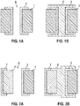
- Fig. 1A shows schematically in the manner of a longitudinal section two workpieces (shell parts of a device shell) 1, which are to be hermetically sealed together by means of the method according to the invention on their mutually facing surfaces
- Fig. 1B shows the workpieces (shell parts) in tightly connected final state.
- the shell parts 1 were each partially provided in advance, in full surface on the surfaces facing each other and additionally in a part of their top and bottom, with a conductive coating 3. They are then fixed with a predetermined gap G between them relative to each other and placed in an electrolytic bath, where galvanically a metal layer 5 is deposited on all metallic surfaces (grows up) and closes the gap G completely and hermetically sealed.
- Fig. 2A again shows two pretreated shell parts 1, 1 ', but with a different material configuration:
- the shell part 1 is again made of an insulating material (such as plastic or ceramic), while the shell part 1' is a metal part.
- the nonconductive member 1 is partially provided with a metal coating 3
- the metallic member is provided with an insulating film 7 on a part of its surfaces to prevent complete coverage with a metal plating layer.
- the parts are brought into a fixed positional relationship with each other and treated under predetermined process conditions in an electrolytic bath, whereby the in Fig. 2B shown configuration is formed.
- all metallic surfaces with a deposited metal layer covered which at the same time fills the original gap between the shell parts 1, 1 'and provides a hermetically sealed joint.
- FIGS. 3A and 3B show a further embodiment, in which two non-conductive parts 1 are connected to the one of the facing surfaces over the entire surface by means of a conductive adhesive 9, after their tops were partially provided with a local metal layer (or even a pressed small metal part) 3 '.
- the parts are only partially immersed in an electrolytic bath, because only their tops (including the free top of the adhesive layer 9) to be provided with a deposited metal layer, and in the electrodeposition process, the top-side metallization forms 5 '.
- This offers in particular a diffusion barrier on the adhesive layer 9 and makes the already existing cohesive connection hermetically sealed.
- the amount of metal consumed for the pretreatment and the electroplating is also significantly lower, and the galvanic process can be completed faster. It also simplifies the alignment of the parts with each other during the electrodeposition.
- FIGS. 4A and 4B a more specific configuration, namely that of a feedthrough 11 of an implantable electromedical device (not shown).
- a titanium flange 1 and a liquid-crystalline polymer material (LCP) -based printed circuit board 15, which pierces the flange perpendicular to its plane of extension, are hermetically sealed together.
- both the surface of the titanium flange 13 and that of the LCP printed circuit board 15 are partially metallized by means of a gold ring 17a or a gold coating 17b.
- This pre-treatment is also required for the titanium flange 13, because its surface carries a natural corrosion layer that would prevent galvanic deposition.
- the annular gap G between them filling and the components are hermetically sealed against each other.
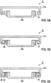
- a further embodiment of the invention is shown schematically in the manner of a longitudinal section in which two titanium shells 23a, 23b of an implant housing 21 are assembled and sealed.
- the half-shells 23a, 23b are provided with a gold coating 27 at the edges.
- a strand conductive adhesive 28 is introduced and cured in the remaining gap between the edges of the fixed in their positional relationship half-shells 23a, 23b.
- a galvanically deposited metal layer 29 then forms on the surfaces of the partial gold layer and the free surface of the conductive adhesive, which makes the implant 23 hermetically sealed.
- the seal is made according to the invention, without the implant being exposed to higher temperatures, as can not be avoided in the laser welding method commonly used.
- FIGS. 6A and 6B Again, in schematic longitudinal cross-sectional views, there is shown a portion of a circuit substrate 33 of an electronic package 31 provided with a protective lid 35. While the lid 35 is made of a metal having a smooth metallic surface which can be electrodeposited without pretreatment, it is deposited on the circuit substrate (e.g. a printed circuit board based on plastic or a ceramic substrate) in turn requires a pre-metallization 37 in the edge area of the lid to be fitted. Alternatively, this metallization can be formed from the same material as the tracks on the substrate and created concurrently with the normal circuit pattern.
- the lid 35 is made of a metal having a smooth metallic surface which can be electrodeposited without pretreatment, it is deposited on the circuit substrate (e.g. a printed circuit board based on plastic or a ceramic substrate) in turn requires a pre-metallization 37 in the edge area of the lid to be fitted.
- this metallization can be formed from the same material as the tracks on the substrate and created concurrently with the normal circuit pattern.
- an adhesive trace 38 is applied from a conductive adhesive, and on this, the lid 35 is placed, so that initially takes place a bonding of the lid to the circuit substrate. Subsequently, a galvanic metallization, which provides the covering and hermetically sealed metal coating 39.
- circuit substrate itself is hermetically sealed (as is the case, for example, with ceramics) or almost hermetically sealed (for example, in the case of an LCP-based printed circuit board), diffusion from the environment into the interior of the sealed assembly is no longer possible.
- a biocompatible, hermetic package can be fabricated without the need for thermal processes above 100 ° C.
- Figs. 7A and 7B show a modification of the last-described embodiment in an assembly 41, which in turn is constructed on a ceramic or plastic substrate 43.
- Main functional component here is a sensor element 44, with corresponding (not separately designated) terminals which extend through the circuit substrate 43 therethrough.
- a hermetic sealing of the peripheral edge of the sensor element 44 on the substrate 43 is required here.
- a galvanically coatable metallization 47 is applied both to the peripheral edge of the sensor element and to the adjacent regions of the substrate 43.
- the non-pre-metallized surface areas of the sensor 44 and the circuit substrate 43 are not electrodepositable due to their lack of conductivity.
- the results in Fig. 7b illustrated configuration with the sensor element annularly partially covering and surrounding deposited metal layer 49. This creates a hermetically sealed connection of the sensor element with the circuit substrate in the edge region of the sensor element.
Landscapes
- Health & Medical Sciences (AREA)
- Engineering & Computer Science (AREA)
- Microelectronics & Electronic Packaging (AREA)
- General Health & Medical Sciences (AREA)
- Biomedical Technology (AREA)
- Life Sciences & Earth Sciences (AREA)
- Animal Behavior & Ethology (AREA)
- Public Health (AREA)
- Veterinary Medicine (AREA)
- Nuclear Medicine, Radiotherapy & Molecular Imaging (AREA)
- Radiology & Medical Imaging (AREA)
- Heart & Thoracic Surgery (AREA)
- Cardiology (AREA)
- Computer Hardware Design (AREA)
- Otolaryngology (AREA)
- Vascular Medicine (AREA)
- Anesthesiology (AREA)
- Hematology (AREA)
- Electromagnetism (AREA)
- Toxicology (AREA)
- Physics & Mathematics (AREA)
- Electrotherapy Devices (AREA)
- Electroplating Methods And Accessories (AREA)
Abstract
Description
- Die Erfindung betrifft eine elektronische Baugruppe, die eine aus mindestens zwei Hüllenteilen zusammengefügte Umhüllung aufweist, und beispielsweise auch ein implantierbares medizinelektronisches Gerät. Sie betrifft des Weiteren ein Verfahren zur Herstellung einer solchen elektronischen Baugruppe.
- Von elektronischen Geräten oder Baugruppen wird in gewissen Anwendungssituationen völlige ("hermetische") Dichtigkeit verlangt. Hierzu zählen Geräte, die unter aggressiven Umweltbedingungen oder auch in einem lebenden Körper dauerhaft zuverlässig arbeiten müssen, also u. a. implantierbare medizinelektronische Geräte. Gelegentlich wird aber auch von speziellen Baugruppen in größeren Geräten oder Vorrichtungen eine solche hermetische Dichtigkeit verlangt.
- Es gibt erprobte Verfahren, um derart dichte elektronische Baugruppen bzw. Geräte mit vertretbarem Aufwand herzustellen. Hierzu zählen - je nach Material und geometrischer Konfiguration der Geräteumhüllung - Schweißverfahren (insbesondere Laserschweißverfahren), Lötverfahren (insbesondere Hartlötverfahren), Sinterverfahren und ähnliche. Bei all diesen Verfahren wird die Baugruppe bzw. das Gerät jedenfalls abschnittsweise einer relativ hohen thermischen Belastung ausgesetzt, die entsprechende thermische Spannungen und ggf. auch gewisse Schädigungen der verwendeten Materialien zur Folge hat. Diese thermischen Spannungen oder gewissen Schädigungen sind grundsätzlich unerwünscht, werden jedoch in der Regel hingenommen. Als grundsätzlicher Nachteil dieser Verfahren ist anzusehen, dass die unvermeidliche thermische Belastung das Spektrum der einsetzbaren Materialien von vornherein einschränkt.
- Es ist daher Aufgabe der Erfindung, eine unter diesen Aspekten verbesserte elektronische Baugruppe und ein Verfahren zur Herstellung einer solchen bereitzustellen, wobei insbesondere thermische Belastungen bei der Herstellung der Hülle und damit einhergehende Beschränkungen der Materialwahl weitestgehend vermieden werden sollen.
- Diese Aufgabe wird in ihrem Vorrichtungsaspekt durch eine elektronische Baugruppe mit den Merkmalen des Anspruchs 1 und in ihrem Verfahrensaspekt durch ein Verfahren mit den Merkmalen des Anspruchs 11 gelöst. Zweckmäßige Fortbildungen des Erfindungsgedankens sind Gegenstand der jeweiligen abhängigen Ansprüche.
- Die Erfindung schließt den Gedanken ein, Spalten zwischen Hüllenteilen der Baugruppe bzw. des Gerätes in einem "kalten" Verfahren und gleichwohl stoffschlüssig zu versiegeln. Sie schließt, angesichts der bekannten Probleme der dauerhaften Aufrechterhaltung hermetischer Dichtigkeit an den Grenzflächen miteinander verbundener Teile, des Weiteren den Gedanken ein, eine Überbrückung bzw. Überdeckung des Spaltbereiches, unter Einschluss der angrenzenden Hüllenteil-Oberflächen, vorzusehen. Schließlich gehört zur Erfindung der Gedanke, diese Überbrückung bzw. Überdeckung mit einer galvanisch mindestens auf die an den Spalt angrenzenden Abschnitte der benachbarten Hüllenteile abgeschiedenen Metallschicht vorzunehmen.
- Ein wesentlicher Vorteil der vorgeschlagenen Lösung besteht im völligen Fortfall jeglicher thermischer Belastung und somit auch der hiermit verbundenen Nachteile, insbesondere thermischer Spannungen und einer Einschränkung der Materialauswahl. Hierbei ist speziell darauf hinzuweisen, dass sich gemäß dem vorgeschlagenen Konzept für den Aufbau der Baugruppen-Hülle auch Materialien mit stark unterschiedlichem thermischen Ausdehnungskoeffizienten (CTE) und Materialien mit sehr geringer thermischer Belastbarkeit einsetzen lassen. Je nach Anwendungsfall, können weitere Vorteile hinzutreten, etwa der Wegfall einer thermischen Belastung der in der Baugruppenhülle aufgenommenen Bauelemente bzw. -teile, eine Reduzierung des Energieaufwandes bei der Herstellung und somit auch der Herstellungskosten usw.
- In einer praktisch wichtigen Ausführung ist die Baugruppe ausgebildet als implantierbares medizinelektronisches Gerät, insbesondere Herzschrittmacher, Kardioverter, Cochlearimplantat oder Medikamentendosierpumpe. Für derartige Geräte ist hermetische Dichtigkeit ein grundlegendes Erfordernis, und die herkömmlichen thermischen Verfahren beispielsweise zur Bildung der sogenannten Durchführung zwischen dem Gehäuse-Hauptteil und dem Kopfteil (Header) eines Schrittmachers oder Kardioverters, teilweise aber auch zur Bildung des Gehäuse-Hauptteils, hatten bisher signifikante Einschränkungen bei der Materialwahl zur Folge. Realisierungen der vorgeschlagenen Baugruppe als vollständig hermetisch dichtes Gerät sind aber nicht auf implantierbare oder allgemeiner medizinelektronische Geräte beschränkt, sondern derartige Geräte können auch bei der Prozesssteuerung in Explorations- oder Chemieanlagen, in der Flugzeugtechnik und Raumfahrt etc. von Bedeutung sein.
- In einer weiteren Ausführung ist die elektronische Baugruppe ausgebildet als hermetisch dichte und optional auch EMI-dichte Komponente eines nicht insgesamt dichten elektronischen Gerätes. Insbesondere kann es sich hierbei um mit einem Deckel bzw. einer Haube versehene Bereiche einer bestückten Leiterplatte oder eines anderen Schaltungssubstrates handeln, an die hinsichtlich der Dichtigkeit höhere Anforderungen als an andere Bereiche bzw. Baugruppen des entsprechenden Gerätes gestellt werden.
- In einer weiteren Ausführung ist mindestens eines der benachbarten Hüllenteile ein Metallteil mit unter der abgeschiedenen Metallschicht metallisch blanker Oberfläche. Das entsprechende Metallteil kann also eines sein, das als solches nicht zur Ausbildung einer natürlichen Oxidschicht (die die galvanische Beschichtung verhindern würde) neigt, also insbesondere Gold oder ein anderes Edelmetall. Es kann aber auch unmittelbar vor der galvanischen Abscheidung einem Reinigungsvorgang unterzogen und/oder vorab mit einem nichtkorrodierenden Metall verbunden oder überzogen worden sein.
- In einer weiteren Ausführung ist mindestens eines der benachbarten Hüllenteile ein Kunststoffteil, insbesondere eine Leiterplatte, oder ein Keramikteil, insbesondere ein Dickschicht-Substrat, mit einer zusätzlichen Metallisierungsschicht unter der abgeschiedenen Metallschicht. Die zusätzliche Metallisierungsschicht (die auch als aufgesetztes oder angefügtes zusätzliches Metallteil realisiert sein kann) sorgt für die erforderliche elektrische Leitfähigkeit für die nachfolgende Metallabscheidung aus dem Elektrolyten. Sie ist grundsätzlich nur in dem Bereich oder entlang einer Kante erforderlich, wo die abdichtende Metallschicht tatsächlich gebildet werden soll.
- In einer weiteren Ausführung der Erfindung sind die einander benachbarten Hüllenteile mit einem Klebstoff verbunden, der den Spaltbereich weitgehend ausfüllt und zumindest an dessen Außenseite leitfähig ist. Hierbei reicht es grundsätzlich aus, wenn der Klebstoff an der äußeren Oberfläche des Spaltes leitfähig ist oder leitfähig gemacht wurde, etwa mit oberflächlich eingebrachtem Metallpulver o. ä.. Typischerweise wird man aber einen homogenen Leitkleber einsetzen, da dies technologisch einfacher ist. Anwendungsbezogen kann beim Einsatz einer mindestens oberflächlich leitfähig gemachten Klebeverbindung davon abgesehen werden, ein elektrisch isolierendes Hüllenteil vorab als solches leitfähig zu machen. Dies wäre insbesondere dann möglich, wenn leitfähiger Klebstoff auch auf den an den Spalt angrenzenden Oberflächenabschnitt des isolierenden Hüllenteils aufgetragen wird, diesen also gewissermaßen "metallisiert".
- In weiteren Ausführungen der Erfindung ist vorgesehen, dass die galvanisch abgeschiedene Metallschicht eine dichte, porenfreie Schicht bildet und so die Diffusion unterbindet. Je nach Anforderungsprofil kann es sich dabei um inerte Metalle wie, z. B. Gold, Platin oder Palladium oder nicht inerte Metalle wie z. B. Cu oder Ni handeln. In einer speziellen Ausführungsform kann die Abscheidung auch mehrere Metalle als Legierung oder Schichtfolge beinhalten. Typische Metallschichtdicken bewegen sich zwischen 0.1 - 100 µm.
- Bei der weiter oben erwähnten Ausführung als medizinelektronisches Gerät kann insbesondere die galvanisch abgeschiedene Metallschicht auf einer Durchführung des medizinelektronischen Gerätes vorgesehen sein und insbesondere den Spaltbereich zwischen einem Flanschteil und einem Leiterelement der Durchführung überbrücken und abdichten. Speziell kann hierbei vorgesehen sein, dass das Flanschteil aus Titan besteht und partiell mit einem Edelmetall-Zusatzteil oder einer Edelmetallschicht versehen ist und das Leiterelement ein Kunststoff- oder Keramiksubstrat aufweist und partiell mit einer Edelmetallschicht versehen ist.
- Des Weiteren kann bei einem solchen implantierbaren Gerät auch das eigentliche Gehäuse erfindungsgemäß aufgebaut sein, also insbesondere aus zwei Gehäuseschalen, der Spaltbereich mit einer galvanisch abgeschiedenen Metallschicht überdeckt und somit hermetisch dicht verschlossen ist.
- In der ebenfalls weiter oben erwähnten Realisierung als einzelne Baugruppe eines größeren Gerätes kann eines der benachbarten Teile eine Leiterplatte oder ein Dickschichtsubstrat und das andere Teil ein metallisches Deckelteil sein und die Leiterplatte oder das Dickschichtsubstrat eine entsprechend der Öffhungskontur des Deckelteils konfigurierte partielle Metallbeschichtung als Unterlage für die galvanisch abgeschiedene Metallschicht aufweisen.
- Verfahrensaspekte der Erfindung in bevorzugten Ausführungen ergeben sich teilweise aus den weiter oben erläuterten Vorrichtungsaspekten und müssen insoweit hier nicht wiederholt werden. Grundsätzlich lassen sich die wesentlichen Schritte des vorgeschlagenen Verfahrens wie folgt darstellen:
- Bereitstellen zweier für eine galvanische Abscheidung inhärent geeigneter oder vorbereiteter Hüllenteile,
- Anordnen der Hüllenteile in einer vorbestimmten Lagebeziehung zueinander, die einen Spaltbereich dazwischen einschließt, und Fixieren der Lagebeziehung der Hüllenteile,
- Verbringen der in ihrer Lagebeziehung fixierten Hüllenteile in ein Elektrolysebad, und
- Ausführen einer galvanischen Abscheidung im Elektrolysebad mit Verfahrensbedingungen, die die Abscheidung einer den Spaltbereich überbrückenden und hermetisch abdichtenden Metallschicht gewährleisten.
- Hierbei ist zu erwähnen, dass die Positionierung der Hüllenteile für die galvanische Beschichtung sinnvollerweise so nahe wie möglich zueinander, also mit möglichst kleinem Spaltbereich, erfolgen wird. Es versteht sich jedoch, dass bei einer Serienproduktion Maßtoleranzen der Hüllenteile zu beachten sind und eine Nachjustierung der Position für jede einzelne Baugruppe bzw. jedes einzelne Gerät mit Blick auf die Kosten normalerweise nicht zweckmäßig sein wird. Hinsichtlich der einzustellenden Verfahrensbedingungen ist zu erwähnen, dass die abgeschiedene Metallschicht hinreichend dick sein muss, um eine dauerhafte hermetische Dichtigkeit im Spaltbereich zu gewährleisten, je nach Anwendungsfall auch bei gewissen mechanischen Beanspruchungen der Baugruppen- bzw. Gerätehülle und/oder bei Temperaturwechselbelastungen im Betrieb.
- In Ausführungen der Erfindung wird die galvanische Abscheidung in einem Elektrolysebad ausgeführt, welches einen dichten Schichtaufbau und eine gute Haftung aufweist. Vorzugweise können Elektrolyte zum Einsatz kommen, die eine beschleunigte Abscheidung in einem Spalt im Vergleich zur Oberfläche ermöglichen (z. B. Dow Chemical EVF).
- In einer weiteren Ausführung weist die galvanisch abgeschiedene Metallschicht mehrere Metalle in Form einer Legierung und/oder einer Schichtfolge mit jeweils unterschiedlichen Metallen in jeder Teilschicht auf.
- In einer noch weiteren Ausführung hat die galvanisch abgeschiedene Metallschicht eine Dicke im Bereich zwischen 0,1 und 100 µm.
- Vorteile und Zweckmäßigkeiten der Erfindung ergeben sich im Übrigen aus der nachfolgenden Beschreibung von Ausführungsbeispielen anhand der Figuren. Von diesen zeigen:
- Fig. 1A und 1B
- Prinzipskizzen zur Erläuterung einer grundsätzlichen Ausführung der Erfindung,
- Fig. 2A und 2B
- Prinzipskizzen zur Erläuterung einer weiteren grundsätzlichen Ausführung der Erfindung,
- Fig. 3A und 3B
- Prinzipskizzen zur Erläuterung einer weiteren grundsätzlichen Ausführung der Erfindung,
- Fig. 4A und 4B
- Prinzipskizzen zur Erläuterung einer Ausführung der Erfindung, bei einem implantierbaren medizinelektronischen Gerät,
- Fig. 5A - 5C
- Prinzipskizzen zur Erläuterung einer weiteren Ausführung der Erfindung, bei einem implantierbaren medizinelektronischen Gerät,
- Fig. 6A und 6B
- Prinzipskizzen zur Erläuterung einer Ausführung der Erfindung, bei einer abgegrenzten elektronischen Baugruppe eines Gerätes, und
- Fig. 7A und 7B
- Prinzipskizzen zur Erläuterung einer weiteren Ausführung der Erfindung, bei einer abgegrenzten elektronischen Baugruppe eines Gerätes.
-
Fig. 1A zeigt schematisch in Art eines Längsschnitts zwei Werkstücke (Hüllenteile einer Gerätehülle) 1, die mittels des erfindungsgemäßen Verfahrens an ihren einander zugewandten Oberflächen hermetisch dicht miteinander verbunden werden sollen, undFig. 1B zeigt die Werkstücke (Hüllenteile) im dicht verbundenen Endzustand. Um das Verfahren anwenden zu können, wurden die Hüllenteile 1 vorab jeweils partiell, und zwar vollflächig an den einander zugewandten Oberflächen und zusätzlich in einem Teil ihrer Ober- und Unterseite, mit einer leitfähigen Beschichtung 3 versehen. Sie werden dann mit einem vorbestimmten Spalt G dazwischen relativ zueinander fixiert und in ein Elektrolysebad gebracht, wo galvanisch eine Metallschicht 5 auf allen metallischen Oberflächen abgeschieden wird (aufwächst) und hierbei den Spalt G vollständig und hermetisch dicht verschließt. -
Fig. 2A zeigt wiederum zwei vorbehandelte Hüllenteile 1, 1', jedoch mit einer anderen Materialkonfiguration: Das Hüllenteil 1 ist wieder aus einem isolierenden Material (etwa Kunststoff oder Keramik) gefertigt, während das Hüllenteil 1' ein Metallteil ist. Wie bei der vorgenannten Ausführung wird zur Ermöglichung der Verfahrensdurchführung das nicht leitende Teil 1 partiell mit einer Metallbeschichtung 3 versehen, wogegen das metallische Teil zur Verhinderung einer vollständigen Bedeckung mit einer galvanisch abgeschiedenen Metallschicht auf einem Teil seiner Oberflächen mit einer Isolierschicht 7 versehen wird. Wiederum werden die Teile in eine feste Positionsbeziehung zueinander gebracht und unter vorbestimmten Prozessbedingungen in einem Elektrolysebad behandelt, wodurch die inFig. 2B gezeigte Konfiguration gebildet wird. Hier sind, ebenso wie bei der ersten Ausführung, sämtliche metallischen Flächen mit einer abgeschiedenen Metallschicht bedeckt, die zugleich den ursprünglichen Spalt zwischen den Hüllenteilen 1, 1' ausfüllt und eine hermetisch dichte Verbindungsstelle liefert. -
Fig. 3A und 3B zeigen eine weitere Ausführung, bei der zwei nichtleitende Teile 1 an den einen der zugewandten Oberflächen vollflächig mittels eines Leitklebers 9 miteinander verbunden werden, nachdem ihre Oberseiten partiell mit einer lokalen Metallschicht (oder auch einem aufgepressten kleinen Metallteil) 3' versehen wurden. Die Teile werden hier nur teilweise in ein Elektrolysebad eingetaucht, weil nur ihre Oberseiten (einschließlich der freien Oberseite der Klebstoffschicht 9) mit einer abgeschiedenen Metallschicht versehen werden sollen, und im galvanischen Abscheidungsprozess bildet sich die Oberseiten-Metallisierung 5'. Diese bietet insbesondere eine Diffusionsbarriere auf der Klebstoffschicht 9 und macht die bereits vorher bestehende stoffschlüssige Verbindung hermetisch dicht. Bei dieser Konfiguration ist auch die Menge des für die Vorbehandlung und die galvanische Beschichtung verbrauchten Metalls deutlich geringer, und der galvanische Prozess kann schneller abgeschlossen werden. Weiterhin vereinfacht es die Ausrichtung der Teile zueinander während der galvanischen Abscheidung. - Während die obigen Ausführungsbeispiele ganz allgemeinen Charakter haben und in ihrer Anwendung nicht auf Hüllenteile einer elektronischen Baugruppe oder bestimmte Geräte beschränkt sind, zeigen
Fig. 4A und 4B eine speziellere Konfiguration, nämlich diejenige einer Durchführung 11 eines implantierbaren elektromedizinischen Gerätes (nicht gezeigt). Hier sollen ein Titanflansch 1 und eine auf einem flüssigkristallinen Polymermaterial (LCP) basierende Leiterplatte 15, die den Flansch senkrecht zu seiner Erstreckungsebene durchstößt, hermetisch dicht miteinander verbunden werden. - Analog wie bei der oben erläuterten ersten und zweiten Ausführung wird sowohl die Oberfläche des Titanflansches 13 als auch diejenige der LCP-Leiterplatte 15 partiell metallisiert, und zwar mittels eines aufgesetzten Goldringes 17a bzw. einer Goldbeschichtung 17b. Diese Vorbehandlung ist auch beim Titanflansch 13 erforderlich, weil dessen Oberfläche eine natürliche Korrosionsschicht trägt, die eine galvanische Abscheidung verhindern würde. In dem in
Fig. 4B gezeigten Endzustand ist eine den Titanflansch und die LCP-Leiterplatte miteinander verbindende, den Ringspalt G zwischen diesen ausfüllende und die Komponenten hermetisch gegeneinander abdichtende Abscheide-Metallisierung 19 ausgebildet. Auch hier besteht eine Abwandlung darin, die Komponenten vorher mittels eines Leitklebers stoffschlüssig miteinander zu verbinden, was insbesondere die Menge des zur Leitfähigmachung der einander zugewandten Oberflächen ansonsten benötigten Goldes reduziert und im Übrigen die Positionierung der Komponenten während der galvanischen Abscheidung vereinfacht. - In
Fig. 5A bis 5C ist eine weitere Ausführung der Erfindung schematisch in Art eines Längsschnittes dargestellt, bei der zwei Titan-Halbschalen 23a, 23b eines Implantatgehäuses 21 zusammengesetzt und abgedichtet werden. Vorab werden die Halbschalen 23a, 23b an den Rändern mit einer Gold-Beschichtung 27 versehen. Anschließend wird in den verbleibenden Spalt zwischen den Rändern der in ihrer Lagebeziehung fixierten Halbschalen 23a, 23b ein Strang Leitkleber 28 eingebracht und ausgehärtet. Im Elektrolysebad bildet sich anschließend auf den Oberflächen der partiellen Goldschicht und der freien Oberfläche des Leitklebers eine galvanisch abgeschiedene Metallschicht 29 aus, die das Implantat 23 hermetisch dicht macht. Die Abdichtung erfolgt erfindungsgemäß, ohne dass das Implantat höheren Temperaturen ausgesetzt wird, wie das beim üblicherweise angewandten Laserschweißverfahren nicht zu vermeiden ist. -
Fig. 6A und 6B zeigen, wiederum in schematischen Längsschnittdarstellungen, einen mit einem schützenden Deckel 35 versehenen Abschnitt eines Schaltungssubstrats 33 einer elektronischen Baugruppe 31. Während der Deckel 35 aus einem Metall mit metallisch blanker Oberfläche besteht, welches ohne Vorbehandlung galvanisch beschichtet werden kann, ist auf dem Schaltungssubstrat (etwa einer Leiterplatte auf Kunststoffbasis oder einem Keramiksubstrat) im Randbereich des aufzusetzenden Deckels wiederum eine Vorab-Metallisierung 37 erforderlich. Alternativ kann diese Metallisierung aus dem gleichen Material wie die Leiterbahnen auf dem Substrat ausgeformt werden und gleichzeitig mit dem normalen Leiterbild erzeugt werden. Auf diese Metallisierung 37 wird eine Klebstoffspur 38 aus einem leitfähigen Klebstoff aufgebracht, und auf diese wird der Deckel 35 aufgesetzt, so dass zunächst eine Verklebung des Deckels mit dem Schaltungssubstrat erfolgt. Anschließend erfolgt eine galvanische Metallisierung, die den abdeckenden und hermetisch dichten Metallüberzug 39 liefert. - Ist das Schaltungssubstrat selbst hermetisch dicht (was zum Beispiel bei Keramik der Fall ist) oder nahezu hermetisch dicht (beispielsweise bei einer LCP-basierten Leiterplatte), ist eine Diffusion aus der Umgebung in das Innere der abgedichteten Baugruppe nicht mehr bzw. kaum noch möglich. In Verbindung mit der den Deckel und die Klebespur überziehenden Metallisierung kann ein biokompatibles, hermetisches Package gefertigt werden, ohne dass thermische Prozesse bei über 100°C eingesetzt werden müssten.
-
Fig. 7A und 7B zeigen eine Abwandlung der zuletzt beschriebenen Ausführung bei einer Baugruppe 41, die wiederum auf einem Keramik- oder Kunststoff-Substrat 43 aufgebaut ist. Haupt-Funktionsbestandteil ist hier ein Sensorelement 44, mit entsprechenden (nicht gesondert bezeichneten) Anschlüssen, die durch das Schaltungssubstrat 43 hindurch verlaufen. Erforderlich ist hier eine hermetische Abdichtung des Umfangsrandes des Sensorelementes 44 auf dem Substrat 43. Hierzu werden zunächst sowohl auf den Umfangsrand des Sensorelementes als auch auf die benachbarten Bereiche des Substrats 43 eine galvanisch beschichtungsfähige Metallisierung 47 aufgebracht. Die nicht vorab metallisierten Oberflächenbereiche des Sensors 44 und des Schaltungssubstrats 43 sind wegen ihrer fehlenden Leitfähigkeit nicht galvanisch beschichtbar. Nach Behandlung im Elektrolysebad ergibt sich die inFig. 7b dargestellte Konfiguration, mit einer das Sensorelement ringförmig partiell bedeckenden und umgebenden abgeschiedenen Metallschicht 49. Diese schafft eine hermetisch dichte Verbindung des Sensorelementes mit dem Schaltungssubstrat im Kantenbereich des Sensorelementes. - Die Ausführung der Erfindung ist nicht auf die oben beschriebenen Beispiele und Aspekte beschränkt, sondern ebenso in einer Vielzahl von Abwandlungen möglich, die im Rahmen fachmännischen Handelns liegen.
Claims (15)
- Elektronische Baugruppe (31, 41), die eine aus mindestens zwei Hüllenteilen (1, 1'; 13, 15; 23a, 23b; 33, 35; 43, 44) zusammengefügte Umhüllung aufweist, wobei mindestens ein Spaltbereich (G) zwischen zwei einander benachbarten Hüllenteilen durch eine mindestens auf an den Spaltbereich angrenzende Abschnitte der benachbarten Hüllenteile galvanisch abgeschiedene, den Spaltbereich überbrückende Metallschicht (5; 19; 29; 39; 49) hermetisch dicht verschlossen ist.
- Elektronische Baugruppe nach Anspruch 1, ausgebildet als implantierbares medizinelektronisches Gerät, insbesondere Herzschrittmacher, Kardioverter, Cochlearimplantat oder Medikamentendosierpumpe.
- Elektronische Baugruppe nach Anspruch 1, ausgebildet als hermetisch dichte und insbesondere EMI-dichte Komponente (31; 41) eines nicht insgesamt dichten elektronischen Gerätes.
- Elektronische Baugruppe nach einem der vorangehenden Ansprüche, wobei mindestens eines der benachbarten Hüllenteile (1, 1'; 13, 15; 23a, 23b; 33, 35; 43, 44) ein Metallteil (1', 23a, 23b; 35) mit unter der abgeschiedenen Metallschicht metallisch blanker Oberfläche ist.
- Elektronische Baugruppe nach einem der vorangehenden Ansprüche, wobei mindestens eines der benachbarten Hüllenteile ein nicht leitender Teil (1; 15; 33; 43), etwa ein Kunststoffteil, insbesondere eine Leiterplatte, oder ein Keramikteil, insbesondere ein Dickschicht-Substrat, mit einer zusätzlichen Metallisierungsschicht (3; 3'; 37; 47) unter der abgeschiedenen Metallschicht (5; 39; 49) ist.
- Elektronische Baugruppe nach einem der vorangehenden Ansprüche, wobei die einander benachbarten Hüllenteile (1; 23a; 23b; 33, 35) mit einem Klebstoff (9; 28; 38) verbunden sind, der den Spaltbereich (G) weitgehend ausfüllt und zumindest an dessen Außenseite leitfähig ist.
- Elektronische Baugruppe nach einem der vorangehenden Ansprüche, wobei die galvanisch abgeschiedene Metallschicht (1, 1'; 13, 15; 23a, 23b; 33, 35; 43, 44) eine dichte, porenfreie Schicht bildet und insbesondere ein inertes Metall wie, z. B. Gold, Platin oder Palladium oder ein nicht inertes Metall wie z. B. Cu oder Ni aufweist.
- Elektronische Baugruppe nach Anspruch 2 und einem der Ansprüche 4 bis 7, wobei die galvanisch abgeschiedene Metallschicht (19) auf einer Durchführung (11) des medizinelektronischen Gerätes vorgesehen ist und insbesondere den Spaltbereich (G) zwischen einem Flanschteil (13) und einem Leiterelement (15) der Durchführung überbrückt und abdichtet.
- Elektronische Baugruppe nach Anspruch 8, wobei das Flanschteil (13) aus Titan besteht und partiell mit einem Edelmetall-Zusatzteil (17a) oder einer Edelmetallschicht versehen ist und das Leiterelement (15) ein Kunststoff- oder Keramiksubstrat aufweist und partiell mit einer Edelmetallschicht (17b) versehen ist.
- Elektronische Baugruppe nach Anspruch 3 und einem der Ansprüche 4 bis 7, wobei eines der benachbarten Teile eine Leiterplatte (33) oder ein Dickschichtsubstrat und das andere Teil ein metallisches Deckelteil (35) ist und die Leiterplatte oder das Dickschichtsubstrat eine entsprechend der Öffnungskontur des Deckelteils konfigurierte partielle Metallbeschichtung (37) als Unterlage für die galvanisch abgeschiedene Metallschicht (39) aufweist.
- Elektronische Baugruppe nach einem der vorangehenden Ansprüche, wobei die galvanisch abgeschiedene Metallschicht mehrere Metalle in Form einer Legierung und/oder einer Schichtfolge mit jeweils unterschiedlichen Metallen in jeder Teilschicht aufweist.
- Elektronische Baugruppe nach einem der vorangehenden Ansprüche, wobei die galvanisch abgeschiedene Metallschicht eine Dicke im Bereich zwischen 0,1 und 100 µm aufweist.
- Verfahren zur Herstellung einer elektronischen Baugruppe nach einem der vorangehenden Ansprüche, welches die Schritte aufweist:Bereitstellen zweier für eine galvanische Abscheidung inhärent geeigneter oder vorbereiteter Hüllenteile(1, 1'; 13, 15; 23a, 23b; 33, 35; 43, 44),Anordnen der Hüllenteile in einer vorbestimmten Lagebeziehung zueinander, die einen Spaltbereich (G) dazwischen einschließt, und Fixieren der Lagebeziehung der Hüllenteile,Verbringen der in ihrer Lagebeziehung fixierten Hüllenteile in ein Elektrolysebad undAusführen einer galvanischen Abscheidung im Elektrolysebad mit Verfahrensbedingungen, die die Abscheidung einer den Spaltbereich überbrückenden und hermetisch abdichtenden Metallschicht (5; 19; 29; 39; 49) gewährleisten.
- Verfahren nach Anspruch 13, wobei das Bereitstellen für eine galvanische Beschichtung vorbereiteter Hüllenteile das mindestens partielle Aufbringen einer Metallisierung (3; 3'; 17b; 37; 47) oder Verbinden mit einem Edelmetallteil (17a) mindestens eines der Hüllenteile (1; 13; 15; 23a; 23b; 33; 43; 44) aufweist.
- Verfahren nach Anspruch 13 oder 14, wobei das Fixieren der Lagebeziehung der Hüllenteile (1; 23a, 23b; 33, 35) deren Verkleben, insbesondere mittels eines Leitklebers und mindestens teilweise Aushärten des Klebers (9; 28; 38) einschließt.
Applications Claiming Priority (1)
| Application Number | Priority Date | Filing Date | Title |
|---|---|---|---|
| DE102016110539.2A DE102016110539A1 (de) | 2016-06-08 | 2016-06-08 | Stoffschlüssige metallische Verbindung basierend auf einer galvanischen Abscheidung |
Publications (2)
| Publication Number | Publication Date |
|---|---|
| EP3254728A1 true EP3254728A1 (de) | 2017-12-13 |
| EP3254728B1 EP3254728B1 (de) | 2020-09-30 |
Family
ID=59030793
Family Applications (1)
| Application Number | Title | Priority Date | Filing Date |
|---|---|---|---|
| EP17174198.6A Active EP3254728B1 (de) | 2016-06-08 | 2017-06-02 | Stoffschlüssige metallische verbindung basierend auf einer galvanischen abscheidung |
Country Status (3)
| Country | Link |
|---|---|
| US (1) | US10154617B2 (de) |
| EP (1) | EP3254728B1 (de) |
| DE (1) | DE102016110539A1 (de) |
Families Citing this family (2)
| Publication number | Priority date | Publication date | Assignee | Title |
|---|---|---|---|---|
| DE102018211186A1 (de) | 2018-07-06 | 2020-01-09 | Biotronik Se & Co. Kg | Implantat mit eingebetteter Leiterbahn und Herstellungsverfahren |
| EP4226957A1 (de) * | 2022-02-10 | 2023-08-16 | F. Hoffmann-La Roche AG | Am körper tragbare medizinische vorrichtung mit dichtungselement |
Citations (3)
| Publication number | Priority date | Publication date | Assignee | Title |
|---|---|---|---|---|
| US20020019669A1 (en) * | 1999-11-29 | 2002-02-14 | Epic Biosonics Inc. | Totally implantable cochlear prosthesis |
| DE102005053765A1 (de) * | 2005-11-10 | 2007-05-16 | Epcos Ag | MEMS-Package und Verfahren zur Herstellung |
| US20090289349A1 (en) * | 2008-05-21 | 2009-11-26 | Spatial Photonics, Inc. | Hermetic sealing of micro devices |
Family Cites Families (9)
| Publication number | Priority date | Publication date | Assignee | Title |
|---|---|---|---|---|
| US4372037A (en) * | 1975-03-03 | 1983-02-08 | Hughes Aircraft Company | Large area hybrid microcircuit assembly |
| JPS58186951A (ja) * | 1982-04-24 | 1983-11-01 | Toshiba Corp | 電子部品のパッケ−ジング方法 |
| US5333095A (en) * | 1993-05-03 | 1994-07-26 | Maxwell Laboratories, Inc., Sierra Capacitor Filter Division | Feedthrough filter capacitor assembly for human implant |
| US5736607A (en) * | 1995-06-05 | 1998-04-07 | Analog Devices, Inc. | Hermetically sealed dies and die attach materials |
| US5750926A (en) * | 1995-08-16 | 1998-05-12 | Alfred E. Mann Foundation For Scientific Research | Hermetically sealed electrical feedthrough for use with implantable electronic devices |
| SE517022C2 (sv) * | 1999-12-07 | 2002-04-02 | Imego Ab | Förseglingsanordning samt metod för hermetisk försegling |
| DE10164494B9 (de) * | 2001-12-28 | 2014-08-21 | Epcos Ag | Verkapseltes Bauelement mit geringer Bauhöhe sowie Verfahren zur Herstellung |
| DE102011112476A1 (de) * | 2011-09-05 | 2013-03-07 | Epcos Ag | Bauelement und Verfahren zum Herstellen eines Bauelements |
| US8946879B2 (en) * | 2012-07-27 | 2015-02-03 | Analog Devices, Inc. | Packages and methods for 3D integration including two stacked dies with a portion of one die extending into a hole of the other die |
-
2016
- 2016-06-08 DE DE102016110539.2A patent/DE102016110539A1/de not_active Withdrawn
-
2017
- 2017-06-02 EP EP17174198.6A patent/EP3254728B1/de active Active
- 2017-06-05 US US15/613,470 patent/US10154617B2/en active Active
Patent Citations (3)
| Publication number | Priority date | Publication date | Assignee | Title |
|---|---|---|---|---|
| US20020019669A1 (en) * | 1999-11-29 | 2002-02-14 | Epic Biosonics Inc. | Totally implantable cochlear prosthesis |
| DE102005053765A1 (de) * | 2005-11-10 | 2007-05-16 | Epcos Ag | MEMS-Package und Verfahren zur Herstellung |
| US20090289349A1 (en) * | 2008-05-21 | 2009-11-26 | Spatial Photonics, Inc. | Hermetic sealing of micro devices |
Also Published As
| Publication number | Publication date |
|---|---|
| EP3254728B1 (de) | 2020-09-30 |
| US20170359924A1 (en) | 2017-12-14 |
| DE102016110539A1 (de) | 2017-12-14 |
| US10154617B2 (en) | 2018-12-11 |
Similar Documents
| Publication | Publication Date | Title |
|---|---|---|
| DE10164502B4 (de) | Verfahren zur hermetischen Verkapselung eines Bauelements | |
| EP2329860B1 (de) | Anschlussgehäuse und dessen Herstellung | |
| DE102016112289B4 (de) | Leiterrahmen und Verfahren zur Herstellung desselben | |
| DE69119969T2 (de) | Elektrisch leitende Abdeckungen, elektrisch leitende Abdeckungen von elektronischen Apparaten und Verfahren zur Herstellung elektrisch leitender Abdeckungen | |
| DE4102019C1 (de) | ||
| DE69629305T2 (de) | Hermetisch abgedichtete elektrische durchführung zur verwendung bei implantierbaren elektronischen vorrichtungen | |
| DE2359851A1 (de) | Verfahren zum vergiessen eines metallstueckes mit einem keramikteil mittels eines lotes | |
| EP3278119B1 (de) | Additives verfahren zur herstellung eines kontaktabstandswandlers sowie kontaktabstandswandler | |
| DE3839891C2 (de) | Verfahren zum Herstellen von Lötschichten auf elektronischen Chip-Bauteilen | |
| DE19606074A1 (de) | Verfahren zum Bilden einer Goldplattierungselektrode, ein Substrat auf Basis des Elektrodenbildungsverfahrens und ein Drahtverbindungsverfahren, das dieses Elektrodenbildungsverfahren anwendet | |
| EP3254728B1 (de) | Stoffschlüssige metallische verbindung basierend auf einer galvanischen abscheidung | |
| EP3229566A1 (de) | Verbindungselement für eine elektronische bauelementanordnung und verfahren zum herstellen desselben, elektronische bauelementanordnung und verfahren zum herstellen desselben | |
| DE19822794C1 (de) | Mehrfachnutzen für elektronische Bauelemente, insbesondere akustische Oberflächenwellen-Bauelemente | |
| DE102014222818A1 (de) | Elektronik-Sandwichstruktur mit zwei mittels einer Sinterschicht zusammengesinterten Fügepartnern | |
| EP2965783B1 (de) | Verfahren zur herstellung eines stifts für eine durchführung eines elektromedizinischen implantats und einer durchführung | |
| DE1102914B (de) | Verfahren zur Herstellung von Halbleiteranordnungen, wie Dioden, Transistoren od. dgl., mit einem Silizium-Halbleiterkoerper | |
| DE3325133A1 (de) | Mikrowellenschaltungsplatte und verfahren zu ihrer herstellung | |
| DE1665771C2 (de) | Verfahren zur Herstellung gedruckter Schaltungsplatten | |
| DE19548062A1 (de) | Elektrisches Bauelement, insbesondere mit akustischen Oberflächenwellen arbeitendes Bauelement - OFW-Bauelement - sowie ein Verfahren zu dessen Herstellung | |
| DE102012213555A1 (de) | Verfahren zur Herstellung eines Substrats für ein Leistungshalbleiterbauelement und Substrat | |
| DE102024119573B3 (de) | Verfahren zum Bilden einer Schaltkreisvorrichtung und Schaltkreisvorrichtung | |
| DE102015121979B4 (de) | Gehäuse für ein elektrisches Bauelement und Verfahren zur Herstellung eines Gehäuses für ein elektrisches Bauelement | |
| DE102009040632B4 (de) | Halbleiter-Bauelement und Verfahren zum Herstellen eines Halbleiter-Bauelements und damit hergestelltes Halbleiter-Bauelement | |
| EP3069759A1 (de) | Implantierbares elektromedizinisches gerät mit einer durchführung mit einem einstückigen kunststoff-grundkörper | |
| DE1043918B (de) | Verfahren zum Verbinden eines nichtmetallischen Stoffes, z. B. Keramik, mit einem Metallteil durch Loeten |
Legal Events
| Date | Code | Title | Description |
|---|---|---|---|
| PUAI | Public reference made under article 153(3) epc to a published international application that has entered the european phase |
Free format text: ORIGINAL CODE: 0009012 |
|
| STAA | Information on the status of an ep patent application or granted ep patent |
Free format text: STATUS: THE APPLICATION HAS BEEN PUBLISHED |
|
| AK | Designated contracting states |
Kind code of ref document: A1 Designated state(s): AL AT BE BG CH CY CZ DE DK EE ES FI FR GB GR HR HU IE IS IT LI LT LU LV MC MK MT NL NO PL PT RO RS SE SI SK SM TR |
|
| AX | Request for extension of the european patent |
Extension state: BA ME |
|
| STAA | Information on the status of an ep patent application or granted ep patent |
Free format text: STATUS: REQUEST FOR EXAMINATION WAS MADE |
|
| 17P | Request for examination filed |
Effective date: 20180611 |
|
| RBV | Designated contracting states (corrected) |
Designated state(s): AL AT BE BG CH CY CZ DE DK EE ES FI FR GB GR HR HU IE IS IT LI LT LU LV MC MK MT NL NO PL PT RO RS SE SI SK SM TR |
|
| GRAP | Despatch of communication of intention to grant a patent |
Free format text: ORIGINAL CODE: EPIDOSNIGR1 |
|
| STAA | Information on the status of an ep patent application or granted ep patent |
Free format text: STATUS: GRANT OF PATENT IS INTENDED |
|
| INTG | Intention to grant announced |
Effective date: 20200424 |
|
| GRAS | Grant fee paid |
Free format text: ORIGINAL CODE: EPIDOSNIGR3 |
|
| GRAA | (expected) grant |
Free format text: ORIGINAL CODE: 0009210 |
|
| STAA | Information on the status of an ep patent application or granted ep patent |
Free format text: STATUS: THE PATENT HAS BEEN GRANTED |
|
| AK | Designated contracting states |
Kind code of ref document: B1 Designated state(s): AL AT BE BG CH CY CZ DE DK EE ES FI FR GB GR HR HU IE IS IT LI LT LU LV MC MK MT NL NO PL PT RO RS SE SI SK SM TR |
|
| REG | Reference to a national code |
Ref country code: CH Ref legal event code: EP Ref country code: GB Ref legal event code: FG4D Free format text: NOT ENGLISH |
|
| REG | Reference to a national code |
Ref country code: DE Ref legal event code: R096 Ref document number: 502017007471 Country of ref document: DE Ref country code: AT Ref legal event code: REF Ref document number: 1318179 Country of ref document: AT Kind code of ref document: T Effective date: 20201015 |
|
| REG | Reference to a national code |
Ref country code: IE Ref legal event code: FG4D Free format text: LANGUAGE OF EP DOCUMENT: GERMAN |
|
| PG25 | Lapsed in a contracting state [announced via postgrant information from national office to epo] |
Ref country code: FI Free format text: LAPSE BECAUSE OF FAILURE TO SUBMIT A TRANSLATION OF THE DESCRIPTION OR TO PAY THE FEE WITHIN THE PRESCRIBED TIME-LIMIT Effective date: 20200930 Ref country code: NO Free format text: LAPSE BECAUSE OF FAILURE TO SUBMIT A TRANSLATION OF THE DESCRIPTION OR TO PAY THE FEE WITHIN THE PRESCRIBED TIME-LIMIT Effective date: 20201230 Ref country code: SE Free format text: LAPSE BECAUSE OF FAILURE TO SUBMIT A TRANSLATION OF THE DESCRIPTION OR TO PAY THE FEE WITHIN THE PRESCRIBED TIME-LIMIT Effective date: 20200930 Ref country code: GR Free format text: LAPSE BECAUSE OF FAILURE TO SUBMIT A TRANSLATION OF THE DESCRIPTION OR TO PAY THE FEE WITHIN THE PRESCRIBED TIME-LIMIT Effective date: 20201231 Ref country code: HR Free format text: LAPSE BECAUSE OF FAILURE TO SUBMIT A TRANSLATION OF THE DESCRIPTION OR TO PAY THE FEE WITHIN THE PRESCRIBED TIME-LIMIT Effective date: 20200930 Ref country code: BG Free format text: LAPSE BECAUSE OF FAILURE TO SUBMIT A TRANSLATION OF THE DESCRIPTION OR TO PAY THE FEE WITHIN THE PRESCRIBED TIME-LIMIT Effective date: 20201230 |
|
| PG25 | Lapsed in a contracting state [announced via postgrant information from national office to epo] |
Ref country code: LV Free format text: LAPSE BECAUSE OF FAILURE TO SUBMIT A TRANSLATION OF THE DESCRIPTION OR TO PAY THE FEE WITHIN THE PRESCRIBED TIME-LIMIT Effective date: 20200930 Ref country code: RS Free format text: LAPSE BECAUSE OF FAILURE TO SUBMIT A TRANSLATION OF THE DESCRIPTION OR TO PAY THE FEE WITHIN THE PRESCRIBED TIME-LIMIT Effective date: 20200930 |
|
| REG | Reference to a national code |
Ref country code: NL Ref legal event code: MP Effective date: 20200930 |
|
| REG | Reference to a national code |
Ref country code: LT Ref legal event code: MG4D |
|
| PG25 | Lapsed in a contracting state [announced via postgrant information from national office to epo] |
Ref country code: EE Free format text: LAPSE BECAUSE OF FAILURE TO SUBMIT A TRANSLATION OF THE DESCRIPTION OR TO PAY THE FEE WITHIN THE PRESCRIBED TIME-LIMIT Effective date: 20200930 Ref country code: SM Free format text: LAPSE BECAUSE OF FAILURE TO SUBMIT A TRANSLATION OF THE DESCRIPTION OR TO PAY THE FEE WITHIN THE PRESCRIBED TIME-LIMIT Effective date: 20200930 Ref country code: CZ Free format text: LAPSE BECAUSE OF FAILURE TO SUBMIT A TRANSLATION OF THE DESCRIPTION OR TO PAY THE FEE WITHIN THE PRESCRIBED TIME-LIMIT Effective date: 20200930 Ref country code: RO Free format text: LAPSE BECAUSE OF FAILURE TO SUBMIT A TRANSLATION OF THE DESCRIPTION OR TO PAY THE FEE WITHIN THE PRESCRIBED TIME-LIMIT Effective date: 20200930 Ref country code: PT Free format text: LAPSE BECAUSE OF FAILURE TO SUBMIT A TRANSLATION OF THE DESCRIPTION OR TO PAY THE FEE WITHIN THE PRESCRIBED TIME-LIMIT Effective date: 20210201 Ref country code: NL Free format text: LAPSE BECAUSE OF FAILURE TO SUBMIT A TRANSLATION OF THE DESCRIPTION OR TO PAY THE FEE WITHIN THE PRESCRIBED TIME-LIMIT Effective date: 20200930 Ref country code: LT Free format text: LAPSE BECAUSE OF FAILURE TO SUBMIT A TRANSLATION OF THE DESCRIPTION OR TO PAY THE FEE WITHIN THE PRESCRIBED TIME-LIMIT Effective date: 20200930 |
|
| PG25 | Lapsed in a contracting state [announced via postgrant information from national office to epo] |
Ref country code: AL Free format text: LAPSE BECAUSE OF FAILURE TO SUBMIT A TRANSLATION OF THE DESCRIPTION OR TO PAY THE FEE WITHIN THE PRESCRIBED TIME-LIMIT Effective date: 20200930 Ref country code: ES Free format text: LAPSE BECAUSE OF FAILURE TO SUBMIT A TRANSLATION OF THE DESCRIPTION OR TO PAY THE FEE WITHIN THE PRESCRIBED TIME-LIMIT Effective date: 20200930 Ref country code: PL Free format text: LAPSE BECAUSE OF FAILURE TO SUBMIT A TRANSLATION OF THE DESCRIPTION OR TO PAY THE FEE WITHIN THE PRESCRIBED TIME-LIMIT Effective date: 20200930 Ref country code: IS Free format text: LAPSE BECAUSE OF FAILURE TO SUBMIT A TRANSLATION OF THE DESCRIPTION OR TO PAY THE FEE WITHIN THE PRESCRIBED TIME-LIMIT Effective date: 20210130 |
|
| PG25 | Lapsed in a contracting state [announced via postgrant information from national office to epo] |
Ref country code: SK Free format text: LAPSE BECAUSE OF FAILURE TO SUBMIT A TRANSLATION OF THE DESCRIPTION OR TO PAY THE FEE WITHIN THE PRESCRIBED TIME-LIMIT Effective date: 20200930 |
|
| REG | Reference to a national code |
Ref country code: DE Ref legal event code: R097 Ref document number: 502017007471 Country of ref document: DE |
|
| PLBE | No opposition filed within time limit |
Free format text: ORIGINAL CODE: 0009261 |
|
| STAA | Information on the status of an ep patent application or granted ep patent |
Free format text: STATUS: NO OPPOSITION FILED WITHIN TIME LIMIT |
|
| PG25 | Lapsed in a contracting state [announced via postgrant information from national office to epo] |
Ref country code: DK Free format text: LAPSE BECAUSE OF FAILURE TO SUBMIT A TRANSLATION OF THE DESCRIPTION OR TO PAY THE FEE WITHIN THE PRESCRIBED TIME-LIMIT Effective date: 20200930 |
|
| 26N | No opposition filed |
Effective date: 20210701 |
|
| PG25 | Lapsed in a contracting state [announced via postgrant information from national office to epo] |
Ref country code: IT Free format text: LAPSE BECAUSE OF FAILURE TO SUBMIT A TRANSLATION OF THE DESCRIPTION OR TO PAY THE FEE WITHIN THE PRESCRIBED TIME-LIMIT Effective date: 20200930 |
|
| PG25 | Lapsed in a contracting state [announced via postgrant information from national office to epo] |
Ref country code: SI Free format text: LAPSE BECAUSE OF FAILURE TO SUBMIT A TRANSLATION OF THE DESCRIPTION OR TO PAY THE FEE WITHIN THE PRESCRIBED TIME-LIMIT Effective date: 20200930 |
|
| PG25 | Lapsed in a contracting state [announced via postgrant information from national office to epo] |
Ref country code: MC Free format text: LAPSE BECAUSE OF FAILURE TO SUBMIT A TRANSLATION OF THE DESCRIPTION OR TO PAY THE FEE WITHIN THE PRESCRIBED TIME-LIMIT Effective date: 20200930 |
|
| GBPC | Gb: european patent ceased through non-payment of renewal fee |
Effective date: 20210602 |
|
| REG | Reference to a national code |
Ref country code: BE Ref legal event code: MM Effective date: 20210630 |
|
| PG25 | Lapsed in a contracting state [announced via postgrant information from national office to epo] |
Ref country code: LU Free format text: LAPSE BECAUSE OF NON-PAYMENT OF DUE FEES Effective date: 20210602 |
|
| PG25 | Lapsed in a contracting state [announced via postgrant information from national office to epo] |
Ref country code: GB Free format text: LAPSE BECAUSE OF NON-PAYMENT OF DUE FEES Effective date: 20210602 |
|
| PG25 | Lapsed in a contracting state [announced via postgrant information from national office to epo] |
Ref country code: IS Free format text: LAPSE BECAUSE OF FAILURE TO SUBMIT A TRANSLATION OF THE DESCRIPTION OR TO PAY THE FEE WITHIN THE PRESCRIBED TIME-LIMIT Effective date: 20210130 Ref country code: FR Free format text: LAPSE BECAUSE OF NON-PAYMENT OF DUE FEES Effective date: 20210630 |
|
| PG25 | Lapsed in a contracting state [announced via postgrant information from national office to epo] |
Ref country code: BE Free format text: LAPSE BECAUSE OF NON-PAYMENT OF DUE FEES Effective date: 20210630 |
|
| PG25 | Lapsed in a contracting state [announced via postgrant information from national office to epo] |
Ref country code: HU Free format text: LAPSE BECAUSE OF FAILURE TO SUBMIT A TRANSLATION OF THE DESCRIPTION OR TO PAY THE FEE WITHIN THE PRESCRIBED TIME-LIMIT; INVALID AB INITIO Effective date: 20170602 |
|
| PG25 | Lapsed in a contracting state [announced via postgrant information from national office to epo] |
Ref country code: CY Free format text: LAPSE BECAUSE OF FAILURE TO SUBMIT A TRANSLATION OF THE DESCRIPTION OR TO PAY THE FEE WITHIN THE PRESCRIBED TIME-LIMIT Effective date: 20200930 |
|
| P01 | Opt-out of the competence of the unified patent court (upc) registered |
Effective date: 20230615 |
|
| REG | Reference to a national code |
Ref country code: AT Ref legal event code: MM01 Ref document number: 1318179 Country of ref document: AT Kind code of ref document: T Effective date: 20220602 |
|
| PG25 | Lapsed in a contracting state [announced via postgrant information from national office to epo] |
Ref country code: AT Free format text: LAPSE BECAUSE OF NON-PAYMENT OF DUE FEES Effective date: 20220602 |
|
| REG | Reference to a national code |
Ref country code: DE Ref legal event code: R082 Ref document number: 502017007471 Country of ref document: DE Representative=s name: SCHULZ JUNGHANS PATENTANWAELTE PARTGMBB, DE Ref country code: DE Ref legal event code: R082 Ref document number: 502017007471 Country of ref document: DE Representative=s name: RANDOLL, SOEREN, DIPL.-CHEM. UNIV. DR. RER. NA, DE Ref country code: DE Ref legal event code: R081 Ref document number: 502017007471 Country of ref document: DE Owner name: DYCONEX AG, CH Free format text: FORMER OWNER: BIOTRONIK SE & CO. KG, 12359 BERLIN, DE |
|
| PG25 | Lapsed in a contracting state [announced via postgrant information from national office to epo] |
Ref country code: MK Free format text: LAPSE BECAUSE OF FAILURE TO SUBMIT A TRANSLATION OF THE DESCRIPTION OR TO PAY THE FEE WITHIN THE PRESCRIBED TIME-LIMIT Effective date: 20200930 |
|
| REG | Reference to a national code |
Ref country code: DE Ref legal event code: R082 Ref document number: 502017007471 Country of ref document: DE Representative=s name: SCHULZ JUNGHANS PATENTANWAELTE PARTGMBB, DE |
|
| PG25 | Lapsed in a contracting state [announced via postgrant information from national office to epo] |
Ref country code: MT Free format text: LAPSE BECAUSE OF FAILURE TO SUBMIT A TRANSLATION OF THE DESCRIPTION OR TO PAY THE FEE WITHIN THE PRESCRIBED TIME-LIMIT Effective date: 20200930 |
|
| PGFP | Annual fee paid to national office [announced via postgrant information from national office to epo] |
Ref country code: DE Payment date: 20250618 Year of fee payment: 9 |
|
| PGFP | Annual fee paid to national office [announced via postgrant information from national office to epo] |
Ref country code: IE Payment date: 20250618 Year of fee payment: 9 |
|
| PGFP | Annual fee paid to national office [announced via postgrant information from national office to epo] |
Ref country code: CH Payment date: 20250701 Year of fee payment: 9 |
|
| PG25 | Lapsed in a contracting state [announced via postgrant information from national office to epo] |
Ref country code: TR Free format text: LAPSE BECAUSE OF FAILURE TO SUBMIT A TRANSLATION OF THE DESCRIPTION OR TO PAY THE FEE WITHIN THE PRESCRIBED TIME-LIMIT Effective date: 20200930 |
|
| REG | Reference to a national code |
Ref country code: CH Ref legal event code: R17 Free format text: ST27 STATUS EVENT CODE: U-0-0-R10-R17 (AS PROVIDED BY THE NATIONAL OFFICE) Effective date: 20260113 |