EP3249448B1 - Sichtwinkel verändernder verbundfilm und anzeigevorrichtung - Google Patents
Sichtwinkel verändernder verbundfilm und anzeigevorrichtung Download PDFInfo
- Publication number
- EP3249448B1 EP3249448B1 EP17169921.8A EP17169921A EP3249448B1 EP 3249448 B1 EP3249448 B1 EP 3249448B1 EP 17169921 A EP17169921 A EP 17169921A EP 3249448 B1 EP3249448 B1 EP 3249448B1
- Authority
- EP
- European Patent Office
- Prior art keywords
- film
- polarizing
- polarizing film
- phase compensation
- composite film
- Prior art date
- Legal status (The legal status is an assumption and is not a legal conclusion. Google has not performed a legal analysis and makes no representation as to the accuracy of the status listed.)
- Active
Links
Images




Classifications
-
- G—PHYSICS
- G02—OPTICS
- G02B—OPTICAL ELEMENTS, SYSTEMS OR APPARATUS
- G02B5/00—Optical elements other than lenses
- G02B5/30—Polarising elements
- G02B5/3025—Polarisers, i.e. arrangements capable of producing a definite output polarisation state from an unpolarised input state
- G02B5/3033—Polarisers, i.e. arrangements capable of producing a definite output polarisation state from an unpolarised input state in the form of a thin sheet or foil, e.g. Polaroid
- G02B5/3041—Polarisers, i.e. arrangements capable of producing a definite output polarisation state from an unpolarised input state in the form of a thin sheet or foil, e.g. Polaroid comprising multiple thin layers, e.g. multilayer stacks
-
- G—PHYSICS
- G02—OPTICS
- G02B—OPTICAL ELEMENTS, SYSTEMS OR APPARATUS
- G02B27/00—Optical systems or apparatus not provided for by any of the groups G02B1/00 - G02B26/00, G02B30/00
- G02B27/28—Optical systems or apparatus not provided for by any of the groups G02B1/00 - G02B26/00, G02B30/00 for polarising
-
- G—PHYSICS
- G02—OPTICS
- G02F—OPTICAL DEVICES OR ARRANGEMENTS FOR THE CONTROL OF LIGHT BY MODIFICATION OF THE OPTICAL PROPERTIES OF THE MEDIA OF THE ELEMENTS INVOLVED THEREIN; NON-LINEAR OPTICS; FREQUENCY-CHANGING OF LIGHT; OPTICAL LOGIC ELEMENTS; OPTICAL ANALOGUE/DIGITAL CONVERTERS
- G02F1/00—Devices or arrangements for the control of the intensity, colour, phase, polarisation or direction of light arriving from an independent light source, e.g. switching, gating or modulating; Non-linear optics
- G02F1/01—Devices or arrangements for the control of the intensity, colour, phase, polarisation or direction of light arriving from an independent light source, e.g. switching, gating or modulating; Non-linear optics for the control of the intensity, phase, polarisation or colour
- G02F1/13—Devices or arrangements for the control of the intensity, colour, phase, polarisation or direction of light arriving from an independent light source, e.g. switching, gating or modulating; Non-linear optics for the control of the intensity, phase, polarisation or colour based on liquid crystals, e.g. single liquid crystal display cells
- G02F1/133—Constructional arrangements; Operation of liquid crystal cells; Circuit arrangements
- G02F1/1333—Constructional arrangements; Manufacturing methods
- G02F1/1335—Structural association of cells with optical devices, e.g. polarisers or reflectors
- G02F1/133528—Polarisers
-
- G—PHYSICS
- G02—OPTICS
- G02F—OPTICAL DEVICES OR ARRANGEMENTS FOR THE CONTROL OF LIGHT BY MODIFICATION OF THE OPTICAL PROPERTIES OF THE MEDIA OF THE ELEMENTS INVOLVED THEREIN; NON-LINEAR OPTICS; FREQUENCY-CHANGING OF LIGHT; OPTICAL LOGIC ELEMENTS; OPTICAL ANALOGUE/DIGITAL CONVERTERS
- G02F1/00—Devices or arrangements for the control of the intensity, colour, phase, polarisation or direction of light arriving from an independent light source, e.g. switching, gating or modulating; Non-linear optics
- G02F1/01—Devices or arrangements for the control of the intensity, colour, phase, polarisation or direction of light arriving from an independent light source, e.g. switching, gating or modulating; Non-linear optics for the control of the intensity, phase, polarisation or colour
- G02F1/13—Devices or arrangements for the control of the intensity, colour, phase, polarisation or direction of light arriving from an independent light source, e.g. switching, gating or modulating; Non-linear optics for the control of the intensity, phase, polarisation or colour based on liquid crystals, e.g. single liquid crystal display cells
- G02F1/133—Constructional arrangements; Operation of liquid crystal cells; Circuit arrangements
- G02F1/1333—Constructional arrangements; Manufacturing methods
- G02F1/1335—Structural association of cells with optical devices, e.g. polarisers or reflectors
- G02F1/1336—Illuminating devices
- G02F1/13362—Illuminating devices providing polarized light, e.g. by converting a polarisation component into another one
-
- G—PHYSICS
- G02—OPTICS
- G02F—OPTICAL DEVICES OR ARRANGEMENTS FOR THE CONTROL OF LIGHT BY MODIFICATION OF THE OPTICAL PROPERTIES OF THE MEDIA OF THE ELEMENTS INVOLVED THEREIN; NON-LINEAR OPTICS; FREQUENCY-CHANGING OF LIGHT; OPTICAL LOGIC ELEMENTS; OPTICAL ANALOGUE/DIGITAL CONVERTERS
- G02F1/00—Devices or arrangements for the control of the intensity, colour, phase, polarisation or direction of light arriving from an independent light source, e.g. switching, gating or modulating; Non-linear optics
- G02F1/01—Devices or arrangements for the control of the intensity, colour, phase, polarisation or direction of light arriving from an independent light source, e.g. switching, gating or modulating; Non-linear optics for the control of the intensity, phase, polarisation or colour
- G02F1/13—Devices or arrangements for the control of the intensity, colour, phase, polarisation or direction of light arriving from an independent light source, e.g. switching, gating or modulating; Non-linear optics for the control of the intensity, phase, polarisation or colour based on liquid crystals, e.g. single liquid crystal display cells
- G02F1/133—Constructional arrangements; Operation of liquid crystal cells; Circuit arrangements
- G02F1/1333—Constructional arrangements; Manufacturing methods
- G02F1/1335—Structural association of cells with optical devices, e.g. polarisers or reflectors
- G02F1/13363—Birefringent elements, e.g. for optical compensation
-
- G—PHYSICS
- G02—OPTICS
- G02B—OPTICAL ELEMENTS, SYSTEMS OR APPARATUS
- G02B5/00—Optical elements other than lenses
- G02B5/30—Polarising elements
- G02B5/3025—Polarisers, i.e. arrangements capable of producing a definite output polarisation state from an unpolarised input state
- G02B5/3033—Polarisers, i.e. arrangements capable of producing a definite output polarisation state from an unpolarised input state in the form of a thin sheet or foil, e.g. Polaroid
-
- G—PHYSICS
- G02—OPTICS
- G02B—OPTICAL ELEMENTS, SYSTEMS OR APPARATUS
- G02B5/00—Optical elements other than lenses
- G02B5/30—Polarising elements
- G02B5/3083—Birefringent or phase retarding elements
-
- G—PHYSICS
- G02—OPTICS
- G02F—OPTICAL DEVICES OR ARRANGEMENTS FOR THE CONTROL OF LIGHT BY MODIFICATION OF THE OPTICAL PROPERTIES OF THE MEDIA OF THE ELEMENTS INVOLVED THEREIN; NON-LINEAR OPTICS; FREQUENCY-CHANGING OF LIGHT; OPTICAL LOGIC ELEMENTS; OPTICAL ANALOGUE/DIGITAL CONVERTERS
- G02F1/00—Devices or arrangements for the control of the intensity, colour, phase, polarisation or direction of light arriving from an independent light source, e.g. switching, gating or modulating; Non-linear optics
- G02F1/01—Devices or arrangements for the control of the intensity, colour, phase, polarisation or direction of light arriving from an independent light source, e.g. switching, gating or modulating; Non-linear optics for the control of the intensity, phase, polarisation or colour
- G02F1/13—Devices or arrangements for the control of the intensity, colour, phase, polarisation or direction of light arriving from an independent light source, e.g. switching, gating or modulating; Non-linear optics for the control of the intensity, phase, polarisation or colour based on liquid crystals, e.g. single liquid crystal display cells
- G02F1/133—Constructional arrangements; Operation of liquid crystal cells; Circuit arrangements
- G02F1/1333—Constructional arrangements; Manufacturing methods
- G02F1/1335—Structural association of cells with optical devices, e.g. polarisers or reflectors
- G02F1/13363—Birefringent elements, e.g. for optical compensation
- G02F1/133633—Birefringent elements, e.g. for optical compensation using mesogenic materials
-
- G—PHYSICS
- G02—OPTICS
- G02F—OPTICAL DEVICES OR ARRANGEMENTS FOR THE CONTROL OF LIGHT BY MODIFICATION OF THE OPTICAL PROPERTIES OF THE MEDIA OF THE ELEMENTS INVOLVED THEREIN; NON-LINEAR OPTICS; FREQUENCY-CHANGING OF LIGHT; OPTICAL LOGIC ELEMENTS; OPTICAL ANALOGUE/DIGITAL CONVERTERS
- G02F2413/00—Indexing scheme related to G02F1/13363, i.e. to birefringent elements, e.g. for optical compensation, characterised by the number, position, orientation or value of the compensation plates
- G02F2413/08—Indexing scheme related to G02F1/13363, i.e. to birefringent elements, e.g. for optical compensation, characterised by the number, position, orientation or value of the compensation plates with a particular optical axis orientation
Definitions
- the invention relates to a composite film and a display device, and particularly relates to a composite film capable of limiting the viewing angle and reducing large-angle light leakage and a display device using the same.
- a display device In order to allow multiple viewers to watch together, a display device usually has a display effect of wide viewing angle.
- a light control film (LCF) is usually placed on a display panel or a backlight module of the conventional display device, so as to filter large-angle light.
- the light control film is quite expensive.
- a periodic structure of the light control film is not only easy to generate Moire pattern with the display device, but also to make overall brightness of the display device decrease by about 30%.
- US 2010/289989 A1 describes an optical element being arranged in such a manner that a screen thereof can be hardly observed from a predetermined direction, and a deterioration of an image quality caused by moire does not occur.
- the optical element is constituted by a first polarizing layer, a second polarizing layer, and a liquid crystal layer arranged between these two polarizing layers.
- absorption axes of the first polarizing layer and the second polarizing layer are located parallel to each other, the liquid crystal layer is made of hybrid-aligned discotic liquid crystal; and an alignment axis of the liquid crystal layer is located parallel to, or perpendicular to both absorption axis of the first polarizing layer and the second polarizing layer.
- US 2009/021657 A1 describes a further viewing angle control film comprising polarizing layers and phase control layers.
- US 2015/346532 A1 describes a liquid display including a liquid crystal display panel having a first substrate and a second substrate.
- An upper polarizer is disposed on an outer surface of the first substrate.
- a viewing angle control film is disposed on the upper polarizer.
- the viewing angle control film includes a polarizing layer having a transmission axis substantially parallel to a transmission axis of the upper polarizer and a phase retardation layer including a birefringence material having an optical axis with a poloidal angle of about 40 degrees to about 75 degrees.
- the invention provides a composite film, which can limit viewing angle and reduce large-angle light leakage.
- the invention also provides a display device using the above composite film, so as to achieve the requirements of anti-spy or viewing angle limitations.
- an embodiment of the invention provides a composite film as specified in appended claim 1.
- an embodiment of the invention provides a display device including a backlight module, a display panel, and the abovementioned composite film.
- the display panel is disposed at one side of the backlight module.
- the composite film is disposed at one side of the backlight module and overlapped with the display panel.
- the embodiments of the invention have at least one of the advantages or effects below.
- the first optical axis of each first phase compensation film is inclined relative to the first polarizing film, and the orthographic projection of the first optical axis on the first polarizing film is parallel to the axial direction of the first transmission axis.
- a polarization direction of a light beam incident the composite film in a large angle along the direction perpendicular to the axial direction of the first transmission axis can be deflected by each first phase compensation film, such that the large-angle light beam is absorbed by the second polarizing film.
- the composite film can limit viewing angle and reduce large-angle light leakage.
- the display device using the composite film can achieve the requirements of anti-spy and viewing angle limitations.
- FIG. 1A and FIG. 1B are schematic cross-sectional diagrams of a composite film on an X-Z plane and on a Y-Z plane according to a first embodiment respectively, wherein the X-Z plane refers to a reference plane constituted by an X direction and a Z direction, and the Y-Z plane refers to a reference plane constituted by a Y direction and the Z direction.
- the X, Y and Z directions are perpendicular to each other.
- a composite film 100 includes a first polarizing film 110, one polarizing film 120 and one first phase compensation film 130 not according to the claimed invention or multiple polarizing films 120 and phase compensation films 130 according to the claimed invention.
- the at least one second polarizing film 120 is disposed at one side of the first polarizing film 110, and the at least one first phase compensation film 130 is disposed between the first polarizing film 110 and the at least one second polarizing film 120.
- the first polarizing film 110 has a first transmission axis T1, which is suitable to convert a light beam incident the composite film 100 into a linearly polarized light oscillating along a specific direction.
- the first polarizing film 110 may be a linear polarizing film.
- the first polarizing film 110 may be composed of a cholesterol liquid crystal layer and a quarter wave plate.
- Each second polarizing film 120 has a second transmission axis T2 parallel to the first transmission axis T1. If the light beam polarized by the first polarizing film 110 is not deflected (i.e., the polarization direction is still parallel to the first transmission axis T1 and the second transmission axis T2) by the at least one first phase compensation film 130 after passing through the at least one first phase compensation film 130, the light beam will pass through the at least one second polarizing film 120.
- each second polarizing film 120 may be an absorption-type polarizing film. The filtration refers to that the polarized light beam is absorbed by the second polarizing film 120.
- Each second polarizing film 120 may be a linear polarizing film.
- each second polarizing film 120 may be composed of a cholesterol liquid crystal layer and a quarter wave plate.
- Each first phase compensation film 130 has a first optical axis T3.
- An orthographic projection PT3 of the first optical axis T3 on the first polarizing film 110 is parallel to an axial direction of the first transmission axis T1, and a first included angle ⁇ 1 between the first optical axis T3 and the first polarizing film 110 is greater than 0 degrees and less than 90 degrees.
- the first optical axis T3 is not perpendicular or parallel to the first polarizing film 110.
- each first phase compensation film 130 is an O-plate, for example.
- each first phase compensation film 130 is composed of a liquid crystal polymer LCP, for example.
- the invention is not limited thereto.
- each first phase compensation film 130 may also be formed from a polymer material by pulling and extension.
- each first phase compensation film 130 may be a liquid crystal panel, and an axial direction of the first optical axis T3 is controlled by electrical control means.
- numbers of the at least one second polarizing film 120 and the at least one first phase compensation film 130 are one respectively. However, the invention is not limited thereto. In other embodiments, the numbers of the at least one second polarizing film 120 and the at least one first phase compensation film 130 may be more than one respectively.
- the non-polarized light beams B1, B2 and B3 include a transverse electric wave TE and a transverse magnetic wave TM respectively, wherein an oscillation direction of the transverse electric wave TE is perpendicular to an incident plane (i.e., paper surface), and an oscillation direction of the transverse magnetic wave TM is parallel to the incident plane.
- the incident plane is the X-Z plane.
- the transverse electric wave TE is oscillated along the direction parallel to the Y direction
- the transverse magnetic wave TM is oscillated on the X-Z plane.
- the axial direction of the first transmission axis T1 of the first polarizing film 110 is parallel to the X direction and perpendicular to the Y and Z directions. Therefore, the transverse magnetic wave TM oscillated on the X-Z plane will pass through the first polarizing film 110, and the transverse electric wave TE oscillated along the direction parallel to the Y direction will be filtered by the first polarizing film 110.
- the first polarizing film 110 may be a reflection-type polarizing film.
- the filtration refers to that the transverse electric wave TE is reflected by the first polarizing film 110 so as to be deflected.
- the first polarizing film 110 may also be an absorption-type polarizing film.
- the filtration refers to that the transverse electric wave TE is absorbed by the first polarizing film 110.
- the incident plane is the Y-Z plane.
- the transverse electric wave TE is oscillated along the direction parallel to the X direction
- the transverse magnetic wave TM is oscillated on the Y-Z plane.
- the axial direction of the first transmission axis T1 of the first polarizing film 110 is parallel to the X direction and perpendicular to the Y and Z directions. Therefore, the transverse magnetic wave TM oscillated on the Y-Z plane will be filtered by the first polarizing film 110, and the transverse electric wave TE oscillated along the direction parallel to the X direction will pass through the first polarizing film 110.
- the polarization directions of the linearly polarized light beams B1', B2' and B3' on polarization planes A, B and C are all parallel to the projection of the first optical axis T3 of the first phase compensation film 130 on the polarization planes A, B and C (referring to the projection of the liquid crystal polymer LCP on the polarization planes A, B and C).
- the polarization direction of the linearly polarized light beams B1', B2' and B3' passing through the first phase compensation film 130 is consistent with the polarization direction of the linearly polarized light beams B1', B2' and B3' passing through the first polarizing film 110, and the linearly polarized light beams B1', B2' and B3' passing through the first phase compensation film 130 may continue passing through the second polarizing film 120.
- the polarization direction of the linearly polarized light B1' forward incident the composite film 100 is parallel to the projection of the first optical axis T3 of the first phase compensation film 130 on the polarization plane A (referring to the projection of the liquid crystal polymer LCP on the polarization plane A).
- the polarization directions of the linearly polarized light beams B2' and B3' i.e., the oscillation direction of the transverse electric wave TE
- the polarization directions of the linearly polarized light beams B2' and B3' are not parallel (including an angle) to the projection of the first optical axis T3 (referring to the projection of the liquid crystal polymer LCP on the polarization planes B and C) of the first phase compensation film 130 on the polarization planes B and C. Therefore, after passing through the first phase compensation film 130, only the linearly polarized light B1' passes through the second polarizing film 120.
- the polarization directions of the linearly polarized light beams B2' and B3' are deflected by the first phase compensation film 130.
- the transverse electric wave TE oscillated along the direction parallel to the X direction originally is converted to the transverse magnetic wave TM oscillated on the Y-Z plane. Since the oscillation direction of the transverse magnetic wave TM is perpendicular to the second transmission axis T2, the linearly polarized light beams B2' and B3' are filtered by the second polarizing film 120 (e.g., absorption).
- the composite film 100 can limit viewing angle along the Y direction and reduce large-angle light leakage along the Y direction.
- the display device using the composite film 100 may achieve the requirements of anti-spy along the Y direction or the limitation of viewing angle along the Y direction and the reduction of large-angle light leakage along the Y direction.
- the composite film 100 can limit viewing angle along the X direction and reduce large-angle light leakage along the X direction.
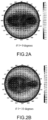
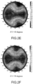
- FIG. 2A to FIG. 2J are viewing angle distribution diagrams of the composite film of FIG. 1A at a first included angle of 0 degrees to 90 degrees respectively. It can be seen from FIG. 2A to FIG. 2J that, when the first included angle ⁇ 1 is between 40 degrees and 80 degrees, on the azimuth of 90 degrees and 270 degrees (i.e., along the Y direction in FIG. 1A and FIG. 1B ), the light intensity is rapidly decreased from the zenith angle of 0 degrees to 90 degrees and is nearly symmetrical on the azimuth of 90 degrees and 270 degrees.
- the composite film 100 not only can limit viewing angle along the Y direction and reduce large-angle light leakage along the Y direction, but also can have the advantage of brightness uniformity.
- the first included angle ⁇ 1 is between 50 degrees and 70 degrees, the effects of narrow viewing angle, reduction of light leakage and brightness uniformity may be further improved.
- the ratio of the linearly polarized light beams B2' and B3' incident the composite film 100 in a large angle along the Y direction filtered by the second polarizing film 120 is related to the amount of phase retardation provided by the first phase compensation film 130.
- the amount of phase retardation is the product of an absolute value of a difference between refractive indexes (e.g., a refractive index ne of a non-ordinary light minus a refractive index no of an ordinary light) of each first phase compensation film 130 and a thickness H130 of the first phase compensation film 130.
- the amount of phase retardation of each first phase compensation film 130 is between 0.1 ⁇ m and 8 ⁇ m, for example, and the thickness H130 of each first phase compensation film 130 is between 1 ⁇ m and 40 ⁇ m, for example.
- FIG. 3 is a schematic cross-sectional diagram of a composite film on the X-Z plane according to an embodiment of the invention.
- FIG. 4 is a diagram illustrating a relationship of light incident angle-transmittance of the composite film of FIG. 3 .
- FIG. 5 and FIG. 6 are schematic diagrams of composite films respectively.
- the main difference between a composite film 200 and the composite film 100 of FIG. 1A is as follows.
- the numbers of the at least one second polarizing film 120 and the at least one first phase compensation film 130 are multiple respectively, and the first phase compensation films 130 are disposed between two adjacent second polarizing films 120 and between the first polarizing film 110 and the second polarizing film 120 closest to the first polarizing film 110 respectively.
- the numbers of the at least one second polarizing film 120 and the at least one first phase compensation film 130 are three respectively.
- the first included angle ⁇ 1 is different, the viewing angle distribution thereof is different. Additionally, the amount of phase retardation of the first phase compensation film 130 is changed with different thickness H130 of the first phase compensation film 130. Thereby, the transmittance curve is also different. Therefore, the embodiment may allow the first included angle ⁇ 1 to be different, and allow the thickness H130 of the first phase compensation film 130 to be different so as to obtain different transmittance curves. Also, the desired transmittance curve is obtained by multiplying each of the transmittance curves.
- the first included angles ⁇ 1 are between 40 degrees and 80 degrees respectively, for example, and the thicknesses H130 of the first phase compensation films 130 corresponding to the first included angles ⁇ 1 between 40 degrees and 80 degrees are between 1 ⁇ m and 40 ⁇ m, for example.
- the structure of the single-layer first polarizing film 110, the single-layer second polarizing film 120 and the single-layer first phase compensation film 130 is adopted by the composite films corresponding to curves C1, C2 and C3 respectively, wherein the structural difference corresponding to the curves C1, C2 and C3 is that the thicknesses H130 of the first phase compensation films 130 are 5 ⁇ m, 6 ⁇ m and 9 ⁇ m respectively, and the first included angles ⁇ 1 are 60 degrees, 62 degrees and 67 degrees respectively.
- the structure of the single-layer first polarizing film 110, the three-layer second polarizing film 120 and the three-layer first phase compensation film 130 is adopted by the composite film corresponding to a curve C4, and the three-layer first phase compensation film 130 adopts the first phase compensation films 130 corresponding to the curves C1, C2 and C3 respectively.
- the structure adopting the three-layer first phase compensation film 130 e.g., as the curve C4 shown
- the structure adopting the three-layer first phase compensation film 130 not only can have better limited viewing angle (the narrowest viewing angle), but also can effectively reduce large-angle light leakage.
- the light transmittance of the light beam of which the incident angle greater than 40 degrees is restricted lower than or equal to 5 %, even close to 0%.
- the composite film 300 includes not only the first polarizing film 110, the at least one second polarizing film 120, and the at least one first phase compensation film 130, but also includes a third polarizing film 310, at least one fourth polarizing film 320, at least one second phase compensation film 330, and a half-wave plate 340.
- the at least one fourth polarizing film 320 is disposed at one side of the third polarizing film 310, and the at least one second phase compensation film 330 is disposed between the third polarizing film 310 and the at least one fourth polarizing film 320.
- the half-wave plate 340 is disposed at one side of the at least one second polarizing film 120 away from the first polarizing film 110 and located between the at least one second polarizing film 120 and the third polarizing film 310.
- the third polarizing film 310 has a third transmission axis T4, and the third transmission axis T4 is perpendicular to the first transmission axis T1.
- Each fourth polarizing film 320 has a fourth transmission axis T5 parallel to the third transmission axis T4.
- the third polarizing film 310 and each fourth polarizing film 320 may be linear polarizing films respectively.
- the third polarizing film 310 and each fourth polarizing film 320 may be composed of a cholesterol liquid crystal layer and a quarter wave plate respectively.
- Each second phase compensation film 330 has a second optical axis T6.
- An orthographic projection PT6 of the second optical axis T6 on the third polarizing film 310 is parallel to an axial direction of the third transmission axis T4, and a second included angle ⁇ 2 between the second optical axis T6 and the third polarizing film 310 is greater than 0 degrees and less than 90 degrees.
- Each second phase compensation film 330 is an O-plate, for example.
- each second phase compensation film 330 is composed of a liquid crystal polymer LCP, for example.
- the invention is not limited thereto. In other embodiments, each second phase compensation film 330 may also be formed from a polymer material by pulling and extension.
- each second phase compensation film 330 may be a liquid crystal panel, and an axial direction of the second optical axis T6 may be controlled by electrical control means.
- the design of the second included angle ⁇ 2 and a thickness H330 of each second phase compensation film 330 can be referred to the related description of the first included angle ⁇ 1 and the thickness H130 of each first phase compensation film 130 in FIG. 1A , and is not repeated herein.
- numbers of the at least one second polarizing film 120, the at least one first phase compensation film 130, the at least one fourth polarizing film 320, and the at least one second phase compensation film 330 are one respectively. In other embodiments, the numbers of the at least one second polarizing film 120, the at least one first phase compensation film 130, the at least one fourth polarizing film 320, and the at least one second phase compensation film 330 may be more than one respectively.
- the composite film 300 can limit viewing angle along the Y direction and reduce large-angle light leakage along the Y direction. Additionally, the polarization direction of the light beam from the at least one second polarizing film 120 can be deflected by the disposition of the half-wave plate 340. For example, the transverse magnetic wave TM oscillated on the X-Z plane originally (referring to FIG. 1A ) is converted to the transverse electric wave TE oscillated along the direction parallel to the Y direction (referring to FIG.
- the composite film 300 can limit viewing angle along the X direction and reduce large-angle light leakage along the X direction.
- the composite film 300 can limit viewing angle along the X direction and the Y direction and reduce large-angle light leakage along the X direction and the Y direction simultaneously.
- the first polarizing film 110 may be an absorption-type polarizing film or a reflection-type polarizing film
- each second polarizing film 120, the third polarizing film 310, and each fourth polarizing film 320 may be absorption-type polarizing films.
- the main difference between a composite film 400 and the composite film 300 of FIG. 5 is as follows.
- the half-wave plate 340 is disposed at one side of the first polarizing film 110 away from the at least one second polarizing film 120 and located between the first polarizing film 110 and the at least one fourth polarizing film 320.
- the third polarizing film 310 may be an absorption-type polarizing film or a reflection-type polarizing film
- each fourth polarizing film 320, the first polarizing film 110, and each second polarizing film 120 may be absorption-type polarizing films.
- FIG. 7 to FIG. 12 are schematic cross-sectional diagrams of display devices on the X-Z plane according to the first embodiment to a sixth embodiment respectively.
- a display device 10 includes a backlight module 12, a display panel 14, and a composite film 16.
- the backlight module 12 is adapted to provide an illumination light beam, which can be a direct-type backlight module or an edge-type backlight module, but is not limited thereto.
- the display panel 14 is disposed at one side of the backlight module 12, which is adapted to convert the illumination light beam provided by the backlight module 12 to a display light beam having display information.
- the display panel 14 may be a liquid crystal display panel, but is not limited thereto.
- the display panel 14 may include a lower polarizing plate 14A, an upper polarizing plate 14B, and a display unit 14C located between the lower polarizing plate 14A and the upper polarizing plate 14B.
- the display unit 14C may include an active element array substrate (not shown), a color filter substrate (not shown), and a liquid crystal layer (not shown) located between the active element array substrate and the color filter substrate.
- the lower polarizing plate 14A and the upper polarizing plate 14B are disposed on two opposite surfaces of the display unit 14C respectively, wherein transmission axes T7 and T8 of the lower polarizing plate 14A and the upper polarizing plate 14B are perpendicular to each other, for example, but is not limited to.
- the composite film 16 is disposed at one side of the backlight module 12 and overlapped with the display panel 14.
- the composite film 16 is disposed between the backlight module 12 and the display panel 14, and the lower polarizing plate 14A is disposed adjacent to the second polarizing film 120. Therefore, the transmission axis T7 of the lower polarizing plate 14A is parallel to the second transmission axis T2 of the second polarizing film 120, such that the polarized illumination light beam incident from the second polarizing film 120 can pass through the lower polarizing plate 14A.
- the composite film 16 may adopt the structure of the composite film 100 as shown in FIG. 1A .
- the composite film 300 can limit viewing angle along a single direction (e.g., Y direction) and reduce large-angle light leakage along a single direction (e.g., Y direction).
- the display device 10 adopting the composite film 16 can achieve the requirements of anti-spy on a single direction (e.g., Y direction) or the limitation of viewing angle along a single direction (e.g., Y direction) and the reduction of large-angle light leakage along a single direction (e.g., Y direction).
- the display device 10 may be a display device for vehicle.
- the first transmission axis T1 and the second transmission axis T2 can be parallel to the Y direction
- the first optical axis T3 can be inclined relative to the Y direction, so as to limit viewing angle along the X direction and reduce large-angle light leakage along the X direction.
- the display device 10 may achieve the requirements of anti-spy along the X direction or the limitation of viewing angle along the X direction and the reduction of large-angle light leakage along the X direction when the display device is a personal computer or a public computer, for example, but is not limited thereto. If it is desired to further improve the effects of anti-spy on a single direction or the limitation of viewing angle along a single direction and the reduction of the large-angle light leakage along a single direction, the numbers of the at least one second polarizing film 120 and the at least one first phase compensation film 130 can be further increased, such as using the structure of the composite film 200 in FIG. 3 .
- the structure of the composite film 300 in FIG. 5 or the structure of the composite film 400 in FIG. 6 can be adopted.
- the following embodiments are applicable to the above improvements, and are not repeated hereinafter.
- the first polarizing film 110 can adopt an absorption-type polarizing film or a reflection-type polarizing film. If the first polarizing film 110 adopts the reflection-type polarizing film, the linearly polarized light of which the polarization direction is perpendicular to the first transmission axis T1 can be reflected back to the backlight module 12 by the first polarizing film 110, so as to effectively improve light utilization; thereby, the brightness of the display device 10 is enhanced.
- the at least one second polarizing film 120 can adopt the absorption-type polarizing film so as to reduce stray light.
- FIG. 8 to FIG. 12 Other embodied forms of the display device are illustrated by the following FIG. 8 to FIG. 12 , wherein the same components are represented by the same notations, and the illustration of the same components is referred to the related description of FIG. 7 , and is not repeated again.
- a transmission axis T7' of a lower polarizing plate 14A' of the display panel 14' is not required to be disposed parallel to the transmission axis T2 of the second polarizing film 120 closest to the lower polarizing plate 14A'.
- the transmission axis T7' is parallel to the Y direction and perpendicular to the transmission axis T2.
- a transmission axis T8' of an upper polarizing plate 14B' of the display panel 14' is parallel to the X direction and perpendicular to the transmission axis T7', for example.
- the display device 10' further includes a half-wave plate 18.
- the half-wave plate 18 is located between the display panel 14' and the composite film 16.
- the polarization direction of the light beam from the at least one second polarizing film 120 can be deflected by the half-wave plate 18, for example, the transverse magnetic wave TM oscillated on the X-Z plane originally (referring to FIG. 1A ) is converted to the transverse electric wave TE oscillated along the direction parallel to the Y direction (referring to FIG. 1A ), such that the polarization direction of the light beam passing through the half-wave plate 18 is parallel to the transmission axis T7' of the lower polarizing plate 14A'.
- the light beam can pass through the lower polarizing plate 14A'.
- the main difference between a display device 20 and the display device 10 of FIG. 7 is as follows.
- the second polarizing film 120 farthest away from the first polarizing film 110 is served as a lower polarizing plate of a display panel 24. That is, the lower polarizing plate 14A of the display panel 14 in FIG. 7 can be omitted in the display panel 24 of the display device 20.
- a polarizing layer in the polarized-type backlight module can be integrated with the first polarizing film 110.
- the polarizing layer in the polarized-type backlight module can be omitted.
- the main difference between a display device 30 and the display device 10 of FIG. 7 is as follows.
- a display panel 34 is disposed between the composite film 16 and the backlight module 12, and the upper polarizing plate 14B of the display panel 34 is disposed adjacent to the first polarizing film 110. Therefore, the transmission axis T8 of the upper polarizing plate 14B is parallel to the first transmission axis T1 of the first polarizing film 110, such that the polarized display light beam incident from the upper polarizing plate 14B can pass through the first polarizing film 110.
- the invention is not limited thereto. As shown in FIG.
- the transmission axis T8' of the upper polarizing plate 14B' of the display panel 34' is not required to be disposed parallel to the first transmission axis T1 of the first polarizing film 110.
- the transmission axis T8' may be perpendicular to the first transmission axis T1 of the first polarizing film 110 and parallel to the Y direction.
- the transmission axis T7' of the lower polarizing plate 14A' of the display panel 34' is parallel to the X direction and perpendicular to the transmission axis T8', for example.
- the display device 30' may further include the half-wave plate 18.
- the half-wave plate 18 is located between the display panel 34' and the composite film 16.
- the polarization direction of the light beam from the upper polarizing plate 14B' can be deflected by the half-wave plate 18, for example, the transverse electric wave TE oscillated along the direction parallel to the Y direction originally (referring to FIG. 1A ) is converted to the transverse magnetic wave TM oscillated on the X-Z plane (referring to FIG. 1A ), such that the polarization direction of the light beam passing through the half-wave plate 18 is parallel to the first transmission axis T1 of the first polarizing film 110.
- the light beam can pass through the first polarizing film 110.
- the first polarizing film 110 and each second polarizing film 120 adopt absorption-type polarizing films so as to reduce stray light.
- the main difference between a display device 40 and the display device 30 of FIG. 10 is as follows.
- the first polarizing film 110 is served as an upper polarizing plate of the display panel 44. That is, the upper polarizing plate 14B of the display panel 34 in FIG. 9 can be omitted in the display panel 44 of the display device 40.
- the embodiments of the invention have at least one of the advantages or effects below.
- the first optical axis of each first phase compensation film is inclined relative to the first polarizing film, and the orthographic projection of the first optical axis on the first polarizing film is parallel to the axial direction of the first transmission axis.
- the polarization direction of the light beam incident the composite film in a large angle along the direction perpendicular to the axial direction of the first transmission axis can be deflected by each first phase compensation film, such that the large-angle light beam is absorbed by the second polarizing film.
- the composite film can limit viewing angle and reduce large-angle light leakage.
- the display device using the composite film can achieve the requirements of anti-spy and viewing angle limitations.
- the term "the invention”, “the present invention” or the like does not necessarily limit the claim scope to a specific embodiment, and the reference to particularly preferred exemplary embodiments of the invention does not imply a limitation on the invention, and no such limitation is to be inferred.
- the claims may refer to use “first”, “second”, etc. following with noun or element. Such terms should be understood as a nomenclature and should not be construed as giving the limitation on the number of the elements modified by such nomenclature unless specific number has been given.
- the abstract of the disclosure is provided to comply with the rules requiring an abstract, which will allow a searcher to quickly ascertain the subject matter of the technical disclosure of any patent issued from this disclosure.
Landscapes
- Physics & Mathematics (AREA)
- General Physics & Mathematics (AREA)
- Optics & Photonics (AREA)
- Nonlinear Science (AREA)
- Mathematical Physics (AREA)
- Chemical & Material Sciences (AREA)
- Crystallography & Structural Chemistry (AREA)
- Polarising Elements (AREA)
- Liquid Crystal (AREA)
Claims (10)
- Verbundfolie (100), die umfasst:mehrere Polarisationsfolien (110, 120), wobei jede Polarisationsfolie eine jeweilige Durchlassachse (T1, T2) besitzt, wobei die Durchlassachsen der Polarisationsfolien zueinander parallel sind; undmehrere Phasenkompensationsfolien (130), wobei jede Phasenkompensationsfolie zwischen zwei benachbarten Polarisationsfolien (110, 120) angeordnet ist, wobei jede Phasenkompensationsfolie (130) eine optische Achse (T3) besitzt, wobei eine orthografische Projektion (PT3) der optischen Achse (T3) auf die Polarisationsfolien (110, 120) parallel zu einer axialen Richtung der Durchlassachsen (T1, T2) ist und ein eingeschlossener Winkel (θ1) zwischen der optischen Achse (T3) und der Polarisationsfolie (110, 120) größer als 0 Grad und kleiner als 90 Grad ist,dadurch gekennzeichnet, dass die Dicken (H130) der Phasenkompensationsfolien (130) voneinander verschieden sind.
- Verbundfolie (100) nach Anspruch 1, wobei die Anzahl der Polarisationsfolien (120) vier ist und jene der Phasenkompensationsfolien (130) drei ist.
- Verbundfolie (100) nach Anspruch 2, wobei die eingeschlossenen Winkel (θ1) zwischen den optischen Achsen (T3) und den Polarisationsfolien (110, 120) voneinander verschieden sind.
- Verbundfolie (100) nach Anspruch 3, wobei die eingeschlossenen Winkel (θ1) jeweils zwischen 40 Grad und 80 Grad liegen und die Dicken der Phasenkompensationsfolien (130), die den eingeschlossenen Winkeln (θ1) zwischen 40 Grad und 80 Grad entsprechen, zwischen 1 µm und 40 µm liegen.
- Verbundfolie (100) nach einem der vorhergehenden Ansprüche, wobei jede Polarisationsfolie (110, 120) eine Polarisationsfolie vom Absorptionstyp ist.
- Verbundfolie (100) nach einem der vorhergehenden Ansprüche, die ferner eine Halbwellenplatte umfasst, die an einer Seite der Polarisationsfolien (110, 120) angeordnet ist.
- Anzeigevorrichtung (10), die umfasst:ein Hintergrundbeleuchtungsmodul (12);eine Anzeigetafel (14), die auf einer Seite des Hintergrundbeleuchtungsmoduls (12) angeordnet ist, undeine Verbundfolie (100) nach einem der Ansprüche 1 bis 6, die auf einer Seite des Hintergrundbeleuchtungsmoduls (12) angeordnet ist und sich mit der Anzeigetafel (14) überschneidet.
- Anzeigevorrichtung (10) nach Anspruch 7, wobei die Anzeigetafel (14) zwischen der Verbundfolie (100) und dem Hintergrundbeleuchtungsmodul (12) angeordnet ist und eine der Polarisationsfolien (110, 120) angrenzend an die Anzeigetafel (14) als eine obere Polarisationsplatte der Anzeigetafel (14) dient.
- Anzeigevorrichtung (10) nach Anspruch 8, wobei die Polarisationsfolien (110, 129) Polarisationsfolien vom Absorptionstyp sind.
- Anzeigevorrichtung (10) nach einem der Ansprüche 7 bis 9, wobei ein Produkt aus einem Absolutwert eines Unterschieds zwischen Brechungsindizes jeder Phasenkompensationsfolie (130) und aus einer Dicke jeder Phasenkompensationsfolie (130) zwischen 0,1 µm und 8 µm liegt.
Applications Claiming Priority (1)
| Application Number | Priority Date | Filing Date | Title |
|---|---|---|---|
| TW105116042A TWI606286B (zh) | 2016-05-24 | 2016-05-24 | 複合膜以及顯示裝置 |
Publications (2)
| Publication Number | Publication Date |
|---|---|
| EP3249448A1 EP3249448A1 (de) | 2017-11-29 |
| EP3249448B1 true EP3249448B1 (de) | 2023-05-31 |
Family
ID=58709235
Family Applications (1)
| Application Number | Title | Priority Date | Filing Date |
|---|---|---|---|
| EP17169921.8A Active EP3249448B1 (de) | 2016-05-24 | 2017-05-08 | Sichtwinkel verändernder verbundfilm und anzeigevorrichtung |
Country Status (5)
| Country | Link |
|---|---|
| US (1) | US10641936B2 (de) |
| EP (1) | EP3249448B1 (de) |
| JP (1) | JP6898146B2 (de) |
| CN (1) | CN107422409B (de) |
| TW (1) | TWI606286B (de) |
Families Citing this family (47)
| Publication number | Priority date | Publication date | Assignee | Title |
|---|---|---|---|---|
| KR102367295B1 (ko) * | 2015-06-26 | 2022-02-23 | 도레이첨단소재 주식회사 | 반사편광자 및 이를 포함하는 백라이트 유닛 |
| US10475418B2 (en) | 2015-10-26 | 2019-11-12 | Reald Spark, Llc | Intelligent privacy system, apparatus, and method thereof |
| WO2017200950A1 (en) | 2016-05-19 | 2017-11-23 | Reald Spark, Llc | Wide angle imaging directional backlights |
| TWM537663U (zh) | 2016-10-25 | 2017-03-01 | 揚昇照明股份有限公司 | 視角控制裝置以及可控制視角顯示裝置 |
| TWI605287B (zh) | 2016-12-29 | 2017-11-11 | 揚昇照明股份有限公司 | 顯示裝置 |
| CN108345139B (zh) | 2017-01-25 | 2022-04-22 | 中强光电股份有限公司 | 视角可切换显示装置 |
| US10126575B1 (en) | 2017-05-08 | 2018-11-13 | Reald Spark, Llc | Optical stack for privacy display |
| CN110809732B (zh) | 2017-05-08 | 2025-01-10 | 瑞尔D斯帕克有限责任公司 | 用于成像定向背光源的光学叠堆 |
| US11327358B2 (en) | 2017-05-08 | 2022-05-10 | Reald Spark, Llc | Optical stack for directional display |
| TWI878209B (zh) | 2017-09-15 | 2025-04-01 | 美商瑞爾D斯帕克有限責任公司 | 顯示裝置及應用於顯示裝置的視角控制光學元件 |
| US10948648B2 (en) | 2017-09-29 | 2021-03-16 | Reald Spark, Llc | Backlights having stacked waveguide and optical components with different coefficients of friction |
| WO2019090246A1 (en) | 2017-11-06 | 2019-05-09 | Reald Spark, Llc | Privacy display apparatus |
| CN207650518U (zh) | 2017-12-26 | 2018-07-24 | 扬升照明股份有限公司 | 视角可切换装置以及视角可切换显示模块 |
| KR102759510B1 (ko) | 2018-01-25 | 2025-02-04 | 리얼디 스파크, 엘엘씨 | 프라이버시 디스플레이를 위한 터치스크린 |
| CA3089476A1 (en) | 2018-01-25 | 2019-08-01 | Reald Spark, Llc | Reflective optical stack for privacy display |
| KR102759511B1 (ko) | 2018-03-22 | 2025-02-03 | 리얼디 스파크, 엘엘씨 | 지향성 백라이트용 광학 도파관 |
| WO2020005748A1 (en) | 2018-06-29 | 2020-01-02 | Reald Spark, Llc | Optical stack for privacy display |
| CN112602011A (zh) | 2018-07-18 | 2021-04-02 | 瑞尔D斯帕克有限责任公司 | 用于可切换定向显示器的光学堆叠 |
| CN109143442A (zh) * | 2018-09-14 | 2019-01-04 | 京东方科技集团股份有限公司 | 一种偏光片、显示模组及显示装置 |
| WO2020072643A1 (en) | 2018-10-03 | 2020-04-09 | Reald Spark, Llc | Privacy display control apparatus |
| US11092852B2 (en) | 2018-11-07 | 2021-08-17 | Reald Spark, Llc | Directional display apparatus |
| US11287677B2 (en) | 2019-01-07 | 2022-03-29 | Reald Spark, Llc | Optical stack for privacy display |
| US11029566B2 (en) | 2019-02-12 | 2021-06-08 | Reald Spark, Llc | Diffuser for privacy display |
| TWI912252B (zh) | 2019-07-02 | 2026-01-21 | 美商瑞爾D斯帕克有限責任公司 | 定向顯示設備 |
| US11099447B2 (en) | 2019-08-02 | 2021-08-24 | Reald Spark, Llc | Optical stack for privacy display |
| CN114730549B (zh) | 2019-10-02 | 2025-07-11 | 瑞尔D斯帕克有限责任公司 | 隐私显示设备 |
| US11733578B2 (en) | 2019-11-13 | 2023-08-22 | ReaID Spark, LLC | Display device with uniform off-axis luminance reduction |
| WO2021118936A1 (en) | 2019-12-10 | 2021-06-17 | Reald Spark, Llc | Control of reflections of a display device |
| EP4440248A3 (de) | 2019-12-18 | 2024-10-16 | RealD Spark, LLC | Umgebungslichtsteuerung für eine datenschutzanzeige |
| US11719868B2 (en) * | 2020-01-06 | 2023-08-08 | Gentex Corporation | Haze matching in a masked display assembly |
| US11353752B2 (en) | 2020-04-30 | 2022-06-07 | Reald Spark, Llc | Directional display apparatus |
| US11237417B2 (en) | 2020-04-30 | 2022-02-01 | Reald Spark, Llc | Directional display apparatus |
| EP4143631A4 (de) | 2020-04-30 | 2024-05-29 | RealD Spark, LLC | Richtungsanzeigegerät |
| US11624944B2 (en) | 2020-07-29 | 2023-04-11 | Reald Spark, Llc | Backlight for switchable directional display |
| TWI898003B (zh) | 2020-07-29 | 2025-09-21 | 美商瑞爾D斯帕克有限責任公司 | 光瞳照明裝置 |
| CN114839815A (zh) * | 2021-02-01 | 2022-08-02 | 中强光电股份有限公司 | 显示装置 |
| US11892717B2 (en) | 2021-09-30 | 2024-02-06 | Reald Spark, Llc | Marks for privacy display |
| CN114200704B (zh) * | 2021-12-10 | 2023-09-26 | 武汉华星光电技术有限公司 | 显示面板及显示装置 |
| TW202332973A (zh) | 2022-02-09 | 2023-08-16 | 美商瑞爾D斯帕克有限責任公司 | 具均勻減低偏軸亮度之顯示裝置 |
| EP4476588A4 (de) | 2022-02-09 | 2025-12-31 | Reald Spark Llc | Beobachterverfolgte privatsphärenanzeige |
| CN119053908A (zh) | 2022-04-07 | 2024-11-29 | 瑞尔D斯帕克有限责任公司 | 定向显示设备 |
| CN115453781B (zh) * | 2022-09-13 | 2025-04-22 | 上海天马微电子有限公司 | 防窥显示模组及显示装置 |
| CN115793324B (zh) * | 2022-12-09 | 2024-02-09 | 厦门天马微电子有限公司 | 显示模组和显示装置 |
| CN116224595B (zh) * | 2023-03-15 | 2025-09-16 | 业成光电(深圳)有限公司 | 平视显示系统及车辆 |
| TW202441227A (zh) | 2023-03-29 | 2024-10-16 | 美商瑞爾D斯帕克有限責任公司 | 角度濾光片標記 |
| JP2026515841A (ja) | 2023-04-25 | 2026-05-19 | リアルディー スパーク エルエルシー | 切り替え可能なプライバシーディスプレイ |
| WO2025030030A2 (en) | 2023-08-03 | 2025-02-06 | Reald Spark, Llc | Privacy displays |
Citations (2)
| Publication number | Priority date | Publication date | Assignee | Title |
|---|---|---|---|---|
| US20090021657A1 (en) * | 2007-07-20 | 2009-01-22 | Yungshun Yang | Viewing angle controllable liquid crystal display |
| US20100149459A1 (en) * | 2007-07-09 | 2010-06-17 | Koji Yabuta | View angle control element and display device provided with the same |
Family Cites Families (56)
| Publication number | Priority date | Publication date | Assignee | Title |
|---|---|---|---|---|
| KR0130554B1 (ko) | 1984-03-19 | 1998-04-11 | 유젠 웬닝거 | 합성수지 매트릭스 및 이에 분산된 액정으로 이루어진 광변조제와 그 제조방법 |
| JPH0580302A (ja) | 1991-09-21 | 1993-04-02 | Semiconductor Energy Lab Co Ltd | 液晶電気光学装置 |
| JP3416302B2 (ja) * | 1994-11-22 | 2003-06-16 | 住友化学工業株式会社 | 液晶ディスプレイ用バックライト装置およびそれを用いた液晶表示装置 |
| US6452650B1 (en) | 1996-09-25 | 2002-09-17 | Matsushita Electric Industrial Co., Ltd. | Polymer dispersion type liquid crystal display element, producing method therefor and apparatus for use in the producing method |
| GB9724781D0 (en) | 1997-11-24 | 1998-01-21 | Ncr Int Inc | Visual displays |
| JP3998897B2 (ja) | 2000-08-11 | 2007-10-31 | セイコーエプソン株式会社 | 液晶表示装置 |
| US6819381B2 (en) | 2002-10-28 | 2004-11-16 | Eastman Kodak Company | Compensation films for liquid crystal displays |
| KR100910559B1 (ko) | 2002-12-24 | 2009-08-03 | 삼성전자주식회사 | 액정 표시 장치 |
| US7201955B2 (en) | 2003-11-26 | 2007-04-10 | E. I. Du Pont De Nemours And Company | Privacy screen for a display |
| JP4369222B2 (ja) | 2003-12-26 | 2009-11-18 | 帝人株式会社 | 広視野角偏光フィルム |
| JP2005266215A (ja) | 2004-03-18 | 2005-09-29 | Toshiba Matsushita Display Technology Co Ltd | 液晶表示装置および抵抗検出式タッチパネル |
| GB2413394A (en) | 2004-04-20 | 2005-10-26 | Sharp Kk | Display |
| JP2006106439A (ja) * | 2004-10-06 | 2006-04-20 | Sharp Corp | 表示装置および電子機器 |
| JP4536489B2 (ja) | 2004-11-15 | 2010-09-01 | 株式会社 日立ディスプレイズ | 光学素子及びそれを用いた表示装置 |
| TWI261124B (en) | 2005-02-22 | 2006-09-01 | Tpo Displays Corp | Liquid crystal display and wide viewing angle crossed polarizer |
| JP3974631B2 (ja) | 2005-03-02 | 2007-09-12 | 日東電工株式会社 | 光学フィルムおよびその製造方法、ならびに該光学フィルムを用いた画像表示装置 |
| WO2006095518A1 (ja) | 2005-03-07 | 2006-09-14 | Nitto Denko Corporation | 液晶パネル、液晶テレビおよび液晶表示装置 |
| EP1930750A1 (de) | 2005-09-09 | 2008-06-11 | Nitto Denko Corporation | Polarisationsplatte mit optischer kompensationsschicht, flüssigkristallschirm mit polarisationsplatte mit optischer kompensationsschicht und bildanzeigeeinheit |
| CN1982976A (zh) * | 2005-12-13 | 2007-06-20 | 奇美电子股份有限公司 | 可切换视角的液晶显示器及其可调变偏光片 |
| KR20070071346A (ko) | 2005-12-30 | 2007-07-04 | 쓰리엠 이노베이티브 프로퍼티즈 컴파니 | 복굴절성 중합체 층을 포함하는 휘도 증강용 광학필름복합체 |
| EP1975689A4 (de) | 2006-01-20 | 2010-01-06 | Nec Corp | Mobiles endgerät |
| TWI320866B (en) | 2006-02-03 | 2010-02-21 | Tpo Displays Corp | Vertical alignment liquid crystal displays |
| US20070236939A1 (en) | 2006-03-31 | 2007-10-11 | 3M Innovative Properties Company | Structured Composite Optical Films |
| US20070236636A1 (en) | 2006-03-31 | 2007-10-11 | Watson Philip E | Contrast ratio enhancement optical stack |
| JP2007279146A (ja) * | 2006-04-03 | 2007-10-25 | Sharp Corp | 視野角制御フィルタおよび表示装置 |
| US20100007818A1 (en) | 2006-06-20 | 2010-01-14 | Nec Corporation | Illumination apparatus, illuminating method and display apparatus |
| JP2008003450A (ja) | 2006-06-26 | 2008-01-10 | Sumitomo Chemical Co Ltd | 複合偏光板、それを用いた液晶表示装置、複合偏光板の製造法及びそれに用いる光学補償フィルムの製造法 |
| US7880843B2 (en) | 2006-07-05 | 2011-02-01 | Sharp Kabushiki Kaisha | Liquid crystal display device and viewing angle control panel |
| US8045097B2 (en) | 2006-08-09 | 2011-10-25 | Sharp Kabushiki Kaisha | Liquid crystal display device and viewing angle control module |
| JP2008096458A (ja) | 2006-10-05 | 2008-04-24 | Sharp Corp | ディスプレイおよびそれに用いられる視野角制御装置 |
| TW200903053A (en) | 2007-07-09 | 2009-01-16 | Shenzhen Tcl Corporate Res Ltd | Optical compound film and LCD using the same |
| CN101414022B (zh) | 2007-10-17 | 2010-10-13 | 财团法人工业技术研究院 | 偏振光学元件、液晶显示器、偏振光源及方法 |
| EP2075601A1 (de) | 2007-12-24 | 2009-07-01 | Lofo High Tech Film GmbH | Optische Kompensationsfolien für Flüssigkristallanzeigen und damit zusammenhängende Erfindungen |
| JP5129682B2 (ja) | 2008-08-04 | 2013-01-30 | スタンレー電気株式会社 | 液晶表示素子 |
| JP2010079287A (ja) | 2008-08-28 | 2010-04-08 | Fujifilm Corp | 液晶表示装置 |
| TW201031969A (en) | 2009-02-18 | 2010-09-01 | Wintek Corp | Image display device and illumination control device |
| KR20100116079A (ko) | 2009-04-21 | 2010-10-29 | 삼성전자주식회사 | 가변 확산 필름을 갖는 표시장치 |
| JP2011002596A (ja) | 2009-06-18 | 2011-01-06 | Mitsubishi Electric Corp | 液晶表示装置 |
| TWI386732B (zh) | 2009-08-19 | 2013-02-21 | Taiwan Tft Lcd Ass | 液晶顯示器以及雙軸補償膜 |
| JP5566785B2 (ja) | 2010-06-22 | 2014-08-06 | 日東電工株式会社 | 複合シート |
| WO2012090769A1 (ja) | 2010-12-28 | 2012-07-05 | シャープ株式会社 | 光学素子、及び、液晶表示装置 |
| US8520176B2 (en) * | 2011-02-01 | 2013-08-27 | Industrial Technology Research Institute | Stereoscopic display module, method for manufacturing the same and manufacturing system thereof |
| CN202141874U (zh) | 2011-07-13 | 2012-02-08 | 京东方科技集团股份有限公司 | 一种偏光调光装置 |
| CN109062448B (zh) | 2013-11-12 | 2021-07-02 | 宸鸿光电科技股份有限公司 | 有机发光二极管触控显示设备 |
| KR20150087494A (ko) | 2014-01-22 | 2015-07-30 | 삼성디스플레이 주식회사 | 윈도우 부재의 제조 방법 |
| JP2015200866A (ja) | 2014-03-31 | 2015-11-12 | 日東電工株式会社 | 光学部材、偏光板のセットおよび液晶表示装置 |
| KR20150137217A (ko) * | 2014-05-28 | 2015-12-09 | 삼성디스플레이 주식회사 | 액정표시장치 |
| KR20170010848A (ko) | 2014-05-30 | 2017-02-01 | 쓰리엠 이노베이티브 프로퍼티즈 컴파니 | 가변 시야각 광학 시스템 |
| WO2016195786A1 (en) | 2015-06-03 | 2016-12-08 | Apple Inc | Electronic device display with switchable film structures |
| US10247982B2 (en) | 2015-06-03 | 2019-04-02 | Apple Inc. | Electronic device display with switchable film structures |
| CN108027470B (zh) | 2015-10-05 | 2020-12-18 | 株式会社Lg化学 | 光学膜 |
| US10705358B2 (en) | 2016-02-02 | 2020-07-07 | Apple, Inc. | Display apparatus with adjustable angles-of-view comprising backlight structures having an electrically adjustable lens array that adjusts backlight illumination |
| CN106168719A (zh) | 2016-08-30 | 2016-11-30 | 深圳市华星光电技术有限公司 | 一种超薄型液晶显示器及其制作方法 |
| TWM537663U (zh) | 2016-10-25 | 2017-03-01 | 揚昇照明股份有限公司 | 視角控制裝置以及可控制視角顯示裝置 |
| US11327358B2 (en) | 2017-05-08 | 2022-05-10 | Reald Spark, Llc | Optical stack for directional display |
| CN110662996B (zh) | 2017-05-29 | 2022-04-19 | 富士胶片株式会社 | 显示装置 |
-
2016
- 2016-05-24 TW TW105116042A patent/TWI606286B/zh active
-
2017
- 2017-05-08 EP EP17169921.8A patent/EP3249448B1/de active Active
- 2017-05-10 JP JP2017093562A patent/JP6898146B2/ja active Active
- 2017-05-10 US US15/591,123 patent/US10641936B2/en active Active
- 2017-05-23 CN CN201710367192.3A patent/CN107422409B/zh active Active
Patent Citations (2)
| Publication number | Priority date | Publication date | Assignee | Title |
|---|---|---|---|---|
| US20100149459A1 (en) * | 2007-07-09 | 2010-06-17 | Koji Yabuta | View angle control element and display device provided with the same |
| US20090021657A1 (en) * | 2007-07-20 | 2009-01-22 | Yungshun Yang | Viewing angle controllable liquid crystal display |
Also Published As
| Publication number | Publication date |
|---|---|
| TW201741748A (zh) | 2017-12-01 |
| JP6898146B2 (ja) | 2021-07-07 |
| US20170343715A1 (en) | 2017-11-30 |
| TWI606286B (zh) | 2017-11-21 |
| CN107422409A (zh) | 2017-12-01 |
| CN107422409B (zh) | 2019-08-09 |
| EP3249448A1 (de) | 2017-11-29 |
| US10641936B2 (en) | 2020-05-05 |
| JP2017211645A (ja) | 2017-11-30 |
Similar Documents
| Publication | Publication Date | Title |
|---|---|---|
| US10641936B2 (en) | Composite film and display device | |
| US11874576B2 (en) | Optical stack for privacy display | |
| US11474397B2 (en) | Optical stack for switchable directional display | |
| US11016318B2 (en) | Optical stack for switchable directional display | |
| US10921622B2 (en) | Anti-peeping control device and backlight module and display using same | |
| CN113167953A (zh) | 定向显示设备 | |
| CN114341681A (zh) | 用于防窥显示器的光学堆叠 | |
| WO2020146091A1 (en) | Optical stack for privacy display | |
| EP3622342A1 (de) | Optischer stapel für direktionale anzeige | |
| US20180210243A1 (en) | Viewing angle switchable display apparatus | |
| KR101096310B1 (ko) | 액정 표시 장치 | |
| JP5145418B2 (ja) | 液晶表示装置 | |
| US20180364405A1 (en) | Polarized type viewing angle control element, polarized type viewing angle control display module, and polarized type viewing angle control light source module | |
| EP3473923A1 (de) | Vorrichtung zur steuerung eines polarisierten betrachtungswinkels, steuergerät für polarisierten betrachtungswinkel und steuerlichtquellenmodul für polarisierten betrachtungswinkel | |
| US20060077325A1 (en) | Cholesteric liquid crystal light control film | |
| US6879356B2 (en) | Optical device having an E-mode polarizer | |
| US20250208453A1 (en) | Anti-peep module and display device | |
| WO2019208263A1 (ja) | 液晶表示装置 | |
| KR101948827B1 (ko) | 투명 액정표시장치 | |
| KR20000065950A (ko) | 보상필름을 이용한 액정표시장치 | |
| KR20080038703A (ko) | 콜레스테릭액정필름을 포함하는 액정표시장치 |
Legal Events
| Date | Code | Title | Description |
|---|---|---|---|
| PUAI | Public reference made under article 153(3) epc to a published international application that has entered the european phase |
Free format text: ORIGINAL CODE: 0009012 |
|
| STAA | Information on the status of an ep patent application or granted ep patent |
Free format text: STATUS: THE APPLICATION HAS BEEN PUBLISHED |
|
| AK | Designated contracting states |
Kind code of ref document: A1 Designated state(s): AL AT BE BG CH CY CZ DE DK EE ES FI FR GB GR HR HU IE IS IT LI LT LU LV MC MK MT NL NO PL PT RO RS SE SI SK SM TR |
|
| AX | Request for extension of the european patent |
Extension state: BA ME |
|
| STAA | Information on the status of an ep patent application or granted ep patent |
Free format text: STATUS: REQUEST FOR EXAMINATION WAS MADE |
|
| 17P | Request for examination filed |
Effective date: 20180517 |
|
| RBV | Designated contracting states (corrected) |
Designated state(s): AL AT BE BG CH CY CZ DE DK EE ES FI FR GB GR HR HU IE IS IT LI LT LU LV MC MK MT NL NO PL PT RO RS SE SI SK SM TR |
|
| RAP1 | Party data changed (applicant data changed or rights of an application transferred) |
Owner name: CORETRONIC CORPORATION |
|
| RAP1 | Party data changed (applicant data changed or rights of an application transferred) |
Owner name: CORETRONIC CORPORATION |
|
| STAA | Information on the status of an ep patent application or granted ep patent |
Free format text: STATUS: EXAMINATION IS IN PROGRESS |
|
| 17Q | First examination report despatched |
Effective date: 20200220 |
|
| GRAP | Despatch of communication of intention to grant a patent |
Free format text: ORIGINAL CODE: EPIDOSNIGR1 |
|
| RIC1 | Information provided on ipc code assigned before grant |
Ipc: G02B 5/30 20060101ALN20221215BHEP Ipc: G02F 1/13363 20060101ALI20221215BHEP Ipc: G02B 27/28 20060101AFI20221215BHEP |
|
| STAA | Information on the status of an ep patent application or granted ep patent |
Free format text: STATUS: GRANT OF PATENT IS INTENDED |
|
| INTG | Intention to grant announced |
Effective date: 20230119 |
|
| GRAS | Grant fee paid |
Free format text: ORIGINAL CODE: EPIDOSNIGR3 |
|
| GRAA | (expected) grant |
Free format text: ORIGINAL CODE: 0009210 |
|
| STAA | Information on the status of an ep patent application or granted ep patent |
Free format text: STATUS: THE PATENT HAS BEEN GRANTED |
|
| AK | Designated contracting states |
Kind code of ref document: B1 Designated state(s): AL AT BE BG CH CY CZ DE DK EE ES FI FR GB GR HR HU IE IS IT LI LT LU LV MC MK MT NL NO PL PT RO RS SE SI SK SM TR |
|
| REG | Reference to a national code |
Ref country code: GB Ref legal event code: FG4D Ref country code: CH Ref legal event code: EP |
|
| REG | Reference to a national code |
Ref country code: DE Ref legal event code: R096 Ref document number: 602017069165 Country of ref document: DE |
|
| REG | Reference to a national code |
Ref country code: AT Ref legal event code: REF Ref document number: 1571275 Country of ref document: AT Kind code of ref document: T Effective date: 20230615 |
|
| REG | Reference to a national code |
Ref country code: IE Ref legal event code: FG4D |
|
| REG | Reference to a national code |
Ref country code: LT Ref legal event code: MG9D |
|
| REG | Reference to a national code |
Ref country code: NL Ref legal event code: MP Effective date: 20230531 |
|
| REG | Reference to a national code |
Ref country code: AT Ref legal event code: MK05 Ref document number: 1571275 Country of ref document: AT Kind code of ref document: T Effective date: 20230531 |
|
| PG25 | Lapsed in a contracting state [announced via postgrant information from national office to epo] |
Ref country code: SE Free format text: LAPSE BECAUSE OF FAILURE TO SUBMIT A TRANSLATION OF THE DESCRIPTION OR TO PAY THE FEE WITHIN THE PRESCRIBED TIME-LIMIT Effective date: 20230531 Ref country code: NO Free format text: LAPSE BECAUSE OF FAILURE TO SUBMIT A TRANSLATION OF THE DESCRIPTION OR TO PAY THE FEE WITHIN THE PRESCRIBED TIME-LIMIT Effective date: 20230831 Ref country code: ES Free format text: LAPSE BECAUSE OF FAILURE TO SUBMIT A TRANSLATION OF THE DESCRIPTION OR TO PAY THE FEE WITHIN THE PRESCRIBED TIME-LIMIT Effective date: 20230531 Ref country code: AT Free format text: LAPSE BECAUSE OF FAILURE TO SUBMIT A TRANSLATION OF THE DESCRIPTION OR TO PAY THE FEE WITHIN THE PRESCRIBED TIME-LIMIT Effective date: 20230531 |
|
| PG25 | Lapsed in a contracting state [announced via postgrant information from national office to epo] |
Ref country code: RS Free format text: LAPSE BECAUSE OF FAILURE TO SUBMIT A TRANSLATION OF THE DESCRIPTION OR TO PAY THE FEE WITHIN THE PRESCRIBED TIME-LIMIT Effective date: 20230531 Ref country code: PL Free format text: LAPSE BECAUSE OF FAILURE TO SUBMIT A TRANSLATION OF THE DESCRIPTION OR TO PAY THE FEE WITHIN THE PRESCRIBED TIME-LIMIT Effective date: 20230531 Ref country code: NL Free format text: LAPSE BECAUSE OF FAILURE TO SUBMIT A TRANSLATION OF THE DESCRIPTION OR TO PAY THE FEE WITHIN THE PRESCRIBED TIME-LIMIT Effective date: 20230531 Ref country code: LV Free format text: LAPSE BECAUSE OF FAILURE TO SUBMIT A TRANSLATION OF THE DESCRIPTION OR TO PAY THE FEE WITHIN THE PRESCRIBED TIME-LIMIT Effective date: 20230531 Ref country code: LT Free format text: LAPSE BECAUSE OF FAILURE TO SUBMIT A TRANSLATION OF THE DESCRIPTION OR TO PAY THE FEE WITHIN THE PRESCRIBED TIME-LIMIT Effective date: 20230531 Ref country code: IS Free format text: LAPSE BECAUSE OF FAILURE TO SUBMIT A TRANSLATION OF THE DESCRIPTION OR TO PAY THE FEE WITHIN THE PRESCRIBED TIME-LIMIT Effective date: 20230930 Ref country code: HR Free format text: LAPSE BECAUSE OF FAILURE TO SUBMIT A TRANSLATION OF THE DESCRIPTION OR TO PAY THE FEE WITHIN THE PRESCRIBED TIME-LIMIT Effective date: 20230531 Ref country code: GR Free format text: LAPSE BECAUSE OF FAILURE TO SUBMIT A TRANSLATION OF THE DESCRIPTION OR TO PAY THE FEE WITHIN THE PRESCRIBED TIME-LIMIT Effective date: 20230901 |
|
| PG25 | Lapsed in a contracting state [announced via postgrant information from national office to epo] |
Ref country code: FI Free format text: LAPSE BECAUSE OF FAILURE TO SUBMIT A TRANSLATION OF THE DESCRIPTION OR TO PAY THE FEE WITHIN THE PRESCRIBED TIME-LIMIT Effective date: 20230531 |
|
| PG25 | Lapsed in a contracting state [announced via postgrant information from national office to epo] |
Ref country code: SK Free format text: LAPSE BECAUSE OF FAILURE TO SUBMIT A TRANSLATION OF THE DESCRIPTION OR TO PAY THE FEE WITHIN THE PRESCRIBED TIME-LIMIT Effective date: 20230531 |
|
| PG25 | Lapsed in a contracting state [announced via postgrant information from national office to epo] |
Ref country code: SM Free format text: LAPSE BECAUSE OF FAILURE TO SUBMIT A TRANSLATION OF THE DESCRIPTION OR TO PAY THE FEE WITHIN THE PRESCRIBED TIME-LIMIT Effective date: 20230531 Ref country code: SK Free format text: LAPSE BECAUSE OF FAILURE TO SUBMIT A TRANSLATION OF THE DESCRIPTION OR TO PAY THE FEE WITHIN THE PRESCRIBED TIME-LIMIT Effective date: 20230531 Ref country code: RO Free format text: LAPSE BECAUSE OF FAILURE TO SUBMIT A TRANSLATION OF THE DESCRIPTION OR TO PAY THE FEE WITHIN THE PRESCRIBED TIME-LIMIT Effective date: 20230531 Ref country code: PT Free format text: LAPSE BECAUSE OF FAILURE TO SUBMIT A TRANSLATION OF THE DESCRIPTION OR TO PAY THE FEE WITHIN THE PRESCRIBED TIME-LIMIT Effective date: 20231002 Ref country code: EE Free format text: LAPSE BECAUSE OF FAILURE TO SUBMIT A TRANSLATION OF THE DESCRIPTION OR TO PAY THE FEE WITHIN THE PRESCRIBED TIME-LIMIT Effective date: 20230531 Ref country code: DK Free format text: LAPSE BECAUSE OF FAILURE TO SUBMIT A TRANSLATION OF THE DESCRIPTION OR TO PAY THE FEE WITHIN THE PRESCRIBED TIME-LIMIT Effective date: 20230531 Ref country code: CZ Free format text: LAPSE BECAUSE OF FAILURE TO SUBMIT A TRANSLATION OF THE DESCRIPTION OR TO PAY THE FEE WITHIN THE PRESCRIBED TIME-LIMIT Effective date: 20230531 |
|
| REG | Reference to a national code |
Ref country code: DE Ref legal event code: R097 Ref document number: 602017069165 Country of ref document: DE |
|
| PLBE | No opposition filed within time limit |
Free format text: ORIGINAL CODE: 0009261 |
|
| STAA | Information on the status of an ep patent application or granted ep patent |
Free format text: STATUS: NO OPPOSITION FILED WITHIN TIME LIMIT |
|
| PG25 | Lapsed in a contracting state [announced via postgrant information from national office to epo] |
Ref country code: SI Free format text: LAPSE BECAUSE OF FAILURE TO SUBMIT A TRANSLATION OF THE DESCRIPTION OR TO PAY THE FEE WITHIN THE PRESCRIBED TIME-LIMIT Effective date: 20230531 |
|
| 26N | No opposition filed |
Effective date: 20240301 |
|
| PG25 | Lapsed in a contracting state [announced via postgrant information from national office to epo] |
Ref country code: SI Free format text: LAPSE BECAUSE OF FAILURE TO SUBMIT A TRANSLATION OF THE DESCRIPTION OR TO PAY THE FEE WITHIN THE PRESCRIBED TIME-LIMIT Effective date: 20230531 Ref country code: IT Free format text: LAPSE BECAUSE OF FAILURE TO SUBMIT A TRANSLATION OF THE DESCRIPTION OR TO PAY THE FEE WITHIN THE PRESCRIBED TIME-LIMIT Effective date: 20230531 |
|
| PG25 | Lapsed in a contracting state [announced via postgrant information from national office to epo] |
Ref country code: BG Free format text: LAPSE BECAUSE OF FAILURE TO SUBMIT A TRANSLATION OF THE DESCRIPTION OR TO PAY THE FEE WITHIN THE PRESCRIBED TIME-LIMIT Effective date: 20230531 |
|
| PG25 | Lapsed in a contracting state [announced via postgrant information from national office to epo] |
Ref country code: BG Free format text: LAPSE BECAUSE OF FAILURE TO SUBMIT A TRANSLATION OF THE DESCRIPTION OR TO PAY THE FEE WITHIN THE PRESCRIBED TIME-LIMIT Effective date: 20230531 |
|
| REG | Reference to a national code |
Ref country code: CH Ref legal event code: PL |
|
| PG25 | Lapsed in a contracting state [announced via postgrant information from national office to epo] |
Ref country code: MC Free format text: LAPSE BECAUSE OF FAILURE TO SUBMIT A TRANSLATION OF THE DESCRIPTION OR TO PAY THE FEE WITHIN THE PRESCRIBED TIME-LIMIT Effective date: 20230531 |
|
| PG25 | Lapsed in a contracting state [announced via postgrant information from national office to epo] |
Ref country code: LU Free format text: LAPSE BECAUSE OF NON-PAYMENT OF DUE FEES Effective date: 20240508 |
|
| GBPC | Gb: european patent ceased through non-payment of renewal fee |
Effective date: 20240508 |
|
| PG25 | Lapsed in a contracting state [announced via postgrant information from national office to epo] |
Ref country code: MC Free format text: LAPSE BECAUSE OF FAILURE TO SUBMIT A TRANSLATION OF THE DESCRIPTION OR TO PAY THE FEE WITHIN THE PRESCRIBED TIME-LIMIT Effective date: 20230531 Ref country code: LU Free format text: LAPSE BECAUSE OF NON-PAYMENT OF DUE FEES Effective date: 20240508 Ref country code: CH Free format text: LAPSE BECAUSE OF NON-PAYMENT OF DUE FEES Effective date: 20240531 |
|
| REG | Reference to a national code |
Ref country code: BE Ref legal event code: MM Effective date: 20240531 |
|
| PG25 | Lapsed in a contracting state [announced via postgrant information from national office to epo] |
Ref country code: IE Free format text: LAPSE BECAUSE OF NON-PAYMENT OF DUE FEES Effective date: 20240508 |
|
| PG25 | Lapsed in a contracting state [announced via postgrant information from national office to epo] |
Ref country code: BE Free format text: LAPSE BECAUSE OF NON-PAYMENT OF DUE FEES Effective date: 20240531 |
|
| PG25 | Lapsed in a contracting state [announced via postgrant information from national office to epo] |
Ref country code: FR Free format text: LAPSE BECAUSE OF NON-PAYMENT OF DUE FEES Effective date: 20240531 |
|
| PG25 | Lapsed in a contracting state [announced via postgrant information from national office to epo] |
Ref country code: GB Free format text: LAPSE BECAUSE OF NON-PAYMENT OF DUE FEES Effective date: 20240508 |
|
| PG25 | Lapsed in a contracting state [announced via postgrant information from national office to epo] |
Ref country code: CY Free format text: LAPSE BECAUSE OF FAILURE TO SUBMIT A TRANSLATION OF THE DESCRIPTION OR TO PAY THE FEE WITHIN THE PRESCRIBED TIME-LIMIT; INVALID AB INITIO Effective date: 20170508 |
|
| PG25 | Lapsed in a contracting state [announced via postgrant information from national office to epo] |
Ref country code: HU Free format text: LAPSE BECAUSE OF FAILURE TO SUBMIT A TRANSLATION OF THE DESCRIPTION OR TO PAY THE FEE WITHIN THE PRESCRIBED TIME-LIMIT; INVALID AB INITIO Effective date: 20170508 |
|
| PG25 | Lapsed in a contracting state [announced via postgrant information from national office to epo] |
Ref country code: TR Free format text: LAPSE BECAUSE OF FAILURE TO SUBMIT A TRANSLATION OF THE DESCRIPTION OR TO PAY THE FEE WITHIN THE PRESCRIBED TIME-LIMIT Effective date: 20230531 |
|
| PGFP | Annual fee paid to national office [announced via postgrant information from national office to epo] |
Ref country code: DE Payment date: 20260527 Year of fee payment: 10 |