EP3234589B1 - Mems-gaschromatograph und verfahren zur formung einer separatorsäule für einen mems-gaschromatographen - Google Patents
Mems-gaschromatograph und verfahren zur formung einer separatorsäule für einen mems-gaschromatographen Download PDFInfo
- Publication number
- EP3234589B1 EP3234589B1 EP15870978.2A EP15870978A EP3234589B1 EP 3234589 B1 EP3234589 B1 EP 3234589B1 EP 15870978 A EP15870978 A EP 15870978A EP 3234589 B1 EP3234589 B1 EP 3234589B1
- Authority
- EP
- European Patent Office
- Prior art keywords
- layer
- device layer
- channel
- trenches
- continuous
- Prior art date
- Legal status (The legal status is an assumption and is not a legal conclusion. Google has not performed a legal analysis and makes no representation as to the accuracy of the status listed.)
- Active
Links
Images






Classifications
-
- G—PHYSICS
- G01—MEASURING; TESTING
- G01N—INVESTIGATING OR ANALYSING MATERIALS BY DETERMINING THEIR CHEMICAL OR PHYSICAL PROPERTIES
- G01N30/00—Investigating or analysing materials by separation into components using adsorption, absorption or similar phenomena or using ion-exchange, e.g. chromatography or field flow fractionation
- G01N30/02—Column chromatography
- G01N30/60—Construction of the column
- G01N30/6095—Micromachined or nanomachined, e.g. micro- or nanosize
-
- B—PERFORMING OPERATIONS; TRANSPORTING
- B81—MICROSTRUCTURAL TECHNOLOGY
- B81B—MICROSTRUCTURAL DEVICES OR SYSTEMS, e.g. MICROMECHANICAL DEVICES
- B81B1/00—Devices without movable or flexible elements, e.g. microcapillary devices
- B81B1/002—Holes characterised by their shape, in either longitudinal or sectional plane
-
- B—PERFORMING OPERATIONS; TRANSPORTING
- B81—MICROSTRUCTURAL TECHNOLOGY
- B81C—PROCESSES OR APPARATUS SPECIALLY ADAPTED FOR THE MANUFACTURE OR TREATMENT OF MICROSTRUCTURAL DEVICES OR SYSTEMS
- B81C1/00—Manufacture or treatment of devices or systems in or on a substrate
- B81C1/00015—Manufacture or treatment of devices or systems in or on a substrate for manufacturing microsystems
- B81C1/00023—Manufacture or treatment of devices or systems in or on a substrate for manufacturing microsystems without movable or flexible elements
- B81C1/00119—Arrangement of basic structures like cavities or channels, e.g. suitable for microfluidic systems
-
- G—PHYSICS
- G01—MEASURING; TESTING
- G01N—INVESTIGATING OR ANALYSING MATERIALS BY DETERMINING THEIR CHEMICAL OR PHYSICAL PROPERTIES
- G01N30/00—Investigating or analysing materials by separation into components using adsorption, absorption or similar phenomena or using ion-exchange, e.g. chromatography or field flow fractionation
- G01N30/02—Column chromatography
- G01N30/60—Construction of the column
-
- G—PHYSICS
- G01—MEASURING; TESTING
- G01N—INVESTIGATING OR ANALYSING MATERIALS BY DETERMINING THEIR CHEMICAL OR PHYSICAL PROPERTIES
- G01N30/00—Investigating or analysing materials by separation into components using adsorption, absorption or similar phenomena or using ion-exchange, e.g. chromatography or field flow fractionation
- G01N30/02—Column chromatography
- G01N2030/022—Column chromatography characterised by the kind of separation mechanism
- G01N2030/025—Gas chromatography
Definitions
- the present invention relates to a method of forming a microelectromechanical system device for a gas chromatograph and a microelectromechanical system device for a gas chromatograph.
- Micro gas chromatography ( ⁇ GC) systems provide a portable, cost effective alternative to conventional gas chromatography (GC) systems and have a wide range of applications in industries such as pharmaceutical, environmental monitoring, petroleum distillation, clinical chemistry, and food processing.
- a typical ⁇ GC system is a hybrid integration of several micro-scale modules such as a preconcentrator, a separation column, a gas detector, and a plurality of micro valves and pumps.
- a ⁇ GC system benefits from a separator column having a smooth sidewall profile to improve measurement accuracy and function as an effective alternative to conventional GC systems.
- Such ⁇ GC systems also benefit from separator columns formed with small channel cross sections and long channel lengths.
- the separator columns of existing ⁇ GC systems are often formed by using an etching process to define the column in the substrate or by using a mold. These manufacturing methods make formation of a smooth sidewall profile difficult due to the inherent limitations of these processes.
- the packaging density of a separator column formed by these existing methods is also limited due the limitations in the scale of the features that can be produced using etching or mold techniques to form the separator column.
- US2014/220723 discloses a method for forming micro-electro-mechanical devices, which involves releasing micro-electro-mechanical structure by etching sacrificial layer with etchant such that portion of sacrificial layer between structure and side of substrate is removed.
- a manufacturing method that enables production of a micro gas chromatograph with atomic smooth channel sidewalls and a high channel packaging density is further desirable.
- MEMS microelectromechanical system
- the one or more atomic-smooth, continuous channels includes a first continuous channel and a second continuous channel
- the device layer defines (i) a first ingress leading into the first continuous channel and a first egress leading out of first continuous channel and (ii) a second ingress leading into the second continuous channel and a second egress leading out of the second continuous channel
- the first continuous channel is disposed substantially along a first plane through the device layer
- the second continuous channel is disposed substantially along a second plane through the device layer
- the first egress of the first continuous channel is joined to the second ingress of the second continuous channel such that first and second continuous channels form a single continuous channel passing through the device layer.
- the method includes etching a trench portion from the upper surface of the device layer to the buried oxide layer, the trench portion encompassing a first portion of the device layer that includes the one or more atomic-smooth, continuous channels, filling the trench portion with an oxide, depositing a passivation layer above the device layer and the oxide-filled trench portion, etching a plurality of vent holes through the passivation layer at locations corresponding to the oxide-filled trench portion, releasing the oxide from within the trench portion to thermally decouple the first portion of the device layer from a second portion of the device layer, and sealing the vent holes, releasing the oxide from within the trench portion includes performing a hydrofluoric acid (HF) vapor etch release, and sealing the vent holes includes performing a clean high temperature seal in an epi reactor.
- HF hydrofluoric acid
- the method includes forming a spacer from the upper surface of the device layer to the buried oxide layer to electrically isolate a side electrode within the device layer prior to etching the plurality of trenches, the spacer positioned proximate to at least a portion of the one or more atomic-smooth continuous channels, depositing a passivation layer above the device layer, the spacer and the side electrode, patterning a portion of the passivation layer to expose the side electrode, depositing a metal layer above the patterned passivation layer and the exposed side electrode, and patterning the metal layer to form a metal portion that is in electrical communication with the side electrode, the metal portion and the side electrode enabling electrostatic biasing of a material conveyed through the one or more atomic-smooth, continuous channels.
- the method includes depositing a passivation layer above the device layer, depositing a metal layer above the passivation layer, patterning the metal layer to form a metal portion proximate to a portion of the one or more atomic-smooth, continuous channels, the metal portion is configured as one more of an upper electrode, a local heater element, and a Seebeck element, the sequential path of the spaced trenches forms one or more of a repeating square wave, a repeating sine wave, a triangular wave, a sawtooth wave, and a meandering path through the device layer when viewed facing the upper surface of the device layer from above, the sequential path of spaced trenches includes trenches that are arranged in one or more of (i) a single-file line, one-trench-behind-the-other-trench and (ii) two or more trenches wide when viewed facing the upper surface of the device layer from above, the one or more atomic-smooth, continuous channels have cross sections that are
- annealing the SOI wafer comprises annealing the SOI wafer in a reducing ambient, at an elevated temperature greater than 1000 degrees Celsius, and for a duration of 10 seconds to 10 minutes, releasing a portion of the buried oxide layer comprises performing a hydrofluoric acid (HF) vapor etch release
- providing an SOI wafer comprises one of providing an SOI wafer having a device layer with a relatively thick layer thickness such that subsequent annealing of the SOI wafer forms at least two atomic-smooth, continuous channels within the device layer, or providing an SOI wafer having a device layer with a relatively thin layer thickness such that subsequent annealing of the SOI wafer forms one atomic-smooth, continuous channel within the device layer.
- MEMS microelectromechanical system
- a side electrode is defined within the released portion of the device layer by a spacer comprising a nitride portion, the side electrode positioned proximate to a portion of the at least one channel, and a metal portion extends through a portion of the passivation layer such that the metal portion is in electrical communication with the side electrode, a trench portion extends between the passivation layer and the cavity, the trench portion encompassing the released portion of the device layer such that the trench portion and the cavity thermally decouple the released portion from an unreleased portion of the device layer, the at least one channel includes a first channel and a second channel, and the released portion of the device layer defines (i) a first ingress leading into the first channel and a first egress leading out of first channel and (ii) a second ingress leading into the second channel and a second egress leading out of the second channel.
- the first channel is disposed substantially along a first plane through the released portion of the device layer
- the second channel is disposed substantially along a second plane through the released portion of the device layer, the second plane spaced from the first plane
- the first and second channels are disposed substantially along a common plane through the released portion of the device layer
- the device layer is a layer of either mono- or poly-crystalline silicon having a thickness of approximately 5 to 50 ⁇ m
- the buried oxide layer has a thickness of approximately 0.5 to 2.5 ⁇ m.
- FIGs. 1 and 2 depict a section view and a top view, respectively, of an electronic device 100 according to a first embodiment.
- the electronic device 100 includes a base layer 102, a buried oxide layer 104, and a device layer 106.
- the buried oxide layer 104 separates the base layer 102 from the device layer 106.
- a cavity 108 etched from a portion of the buried oxide layer 104 isolates a portion of the base layer 102 from the device layer 106.
- the device layer 106 is anchored to the base layer 102 by a portion 105 of the buried oxide layer 104 that remains after the etching of the cavity 108.
- a continuous first channel 110 is disposed between an upper surface 112 and a lower surface 114 of the device layer 106.
- the first channel 110 in the embodiment shown extends substantially along a first plane spaced between the upper and the lower surfaces 112, 114. In other embodiments, the first channel 110 extends in a variable manner along, above, and/or below the first plane such that the first channel 110 forms a first undulating channel enclosed within the device layer 106.
- the electronic device 100 also includes a continuous second channel 134 disposed between the upper surface 112 and the first channel 110 within the cap layer 106.
- the second channel 134 in the embodiment shown extends substantially along a second plane spaced between the upper surface 112 and the first channel 110.
- the second channel 134 extends in a variable manner along, above, and/or below the second plane such that the second channel 134 forms an undulating channel enclosed within the device layer 106.
- the first channel 110 and the second channel 134 are aligned such that the path of the first channel 110 through the cap layer 106 is shown as identical to the path of the second channel 134 through the cap layer 106.
- the path of the first channel 110 includes at least some portions that are different than the path of the second channel 134.
- the first channel 110 and the second channel 134 are configured to enable a material, such as a gaseous composition, to pass through the channels 110, 134 between at least one ingress portion and at least one egress portion.
- the first channel 110 includes a first ingress portion (not shown) that enables the material to enter the first channel 110 and a first egress portion (not shown) that enables material to exit the first channel 210.
- the second channel 134 includes a second ingress portion 136 that allows material to enter the second channel 134 and a second egress portion 138 that enables material to exit the second channel 134.
- first channel 110 and the second channel 134 are joined such that the material enters the channels 110, 134 at the ingress portion of one channel, passes through the channels 110, 134, and exits the channels 110, 134 at the egress portion of the other channel.
- the ingress portion 136 and the egress portion 138 of the second channel 134 are shown at specific locations in FIG. 2 , these portions 136, 138 in other embodiments can be located at different positions in the device layer 106. Similarly, the ingress and the egress portions of the first channel 110 can be located at different positions in the device layer 106. In embodiments with the first channel 110 and the second channel 134 joined, the ingress portion and the egress portion can also be located at positions different than those positions depicted in FIG. 2 .
- the first channel 110 is shown having an oval-shaped cross section when viewed along a section plane that passes perpendicular to the path of the channel through the device layer 106. In other embodiments, the first channel 110 has a cross section different than the oval-shaped cross section.
- the cross section of the first channel in any embodiment can be constant, variable, or can include both constant and variable portions along the channel path.
- the second channel 134 is also shown having an oval-shaped cross section when viewed along the section plane. In other embodiments, the second channel 134 has a cross section different than the oval-shaped cross section.
- the cross section of the second channel 134 in any embodiment can be constant, variable, or can include both constant and variable portions along the channel path. In some embodiments, at least some portions of the first channel 110 have cross sections that are different than the cross section of the second channel 134.
- the electronic device 100 is shown with a passivation layer 116 located above the device layer 106.
- a first metal portion 118 is disposed above the passivation layer 116 and positioned proximate to at least a portion of the channels 110, 134.
- the first metal portion 118 is configured as an upper electrode that electrostatically biases the material that passes through the portion of the channels 110, 134 near the upper electrode.
- the first metal portion 118 in other embodiments is configured as a local heater element that locally heats the material passing through the channels 110, 134 near the heater element.
- the first metal portion 118 is configured as a Seebeck element utilizing the Seebeck effect to actively heat or cool the material passing through the channel 110, 134.
- the passivation layer 116 in any of these embodiments electrically insulates the first metal portion 118 from the device layer 106.
- the electronic device 100 further includes a side electrode 122 defined within the device layer 106 by at least one spacer 124.
- the spacer 124 includes a nitride portion that extends through the device layer 106 and between the cavity 108 and the passivation layer 116 to electrically insulate the side electrode 122 from the device layer 106.
- the passivation layer 116 includes a contact portion that enables a second metal portion 119 to contact the side electrode 122 for electrical communication therebetween.
- the side electrode 122 is positioned proximate to at least a portion of the channels 110, 134 such that side electrode 122 can electrostatically bias the material passing through the portion of the channels 110, 134 near the side electrode 122.
- a trench portion 132 extends through the device layer 106 and between the passivation layer 116 and the cavity 108 to isolate a first portion 128 of the device layer 106 from a second portion 130 of the device layer. As shown in the figures, the first and the second channels 110, 134 are substantially encompassed within the first portion 128 of the device layer 106. The trench portion 132 and the cavity 108 are configured to thermally decouple the first portion 128 of the device layer 106 from the second portion 130 of the device layer 106.
- the passivation layer 116 substantially supports the first portion 128 of the device layer 106 and anchors the first portion 128 to the base layer 102 by connection to the second portion 130 of the device layer 106, which in turn is connected to the buried oxide portion 105.
- FIGs. 3-6 depict alternative embodiments of an electronic device provided by omitting and/or combining selected features of the electronic device 100 of FIG. 1 .
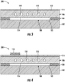
- FIG. 3 shows an electronic device 200 including only the first channel 110 within the device layer 106.
- the device layer 106 is a layer of either mono- or poly-crystalline silicon having a thickness of approximately 5 to 50 ⁇ m.
- the buried oxide layer 104 is shown having a thickness of approximately 0.5 to 2.5 ⁇ m
- FIG. 4 depicts the electronic device 200 of FIG. 3 with only the first metal portion 118 disposed above the passivation layer 116 and positioned proximate to the first channel 110.
- the first metal portion 118 can be configured as one or more of an upper electrode, a local heater element, and a Seebeck element.
- FIG. 5 shows the electronic device 200 of FIG. 3 with only the side electrode 122 defined within the device layer 106.
- the side electrode 122 is positioned proximate to at least a portion of the channel 110 such that side electrode 122 can electrostatically bias the material passing through the portion of the channel 110 near the side electrode 122.
- FIG. 6 depicts the electronic device 200 of FIG.3 with only the trench portion 132 disposed within the device layer 106 to thermally decouple the first portion 128 of the device layer 106 from the second portion 130.
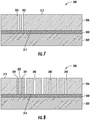
- a silicon-on-insulator (SOI) wafer 300 including a base layer 302, a buried oxide layer 304, and a device layer 306 is initially etched to define a first trench portion 325 through the device layer 306 and between an upper surface 312 and a lower surface 314 of the device layer 306.
- the first trench portion 325 is filled with a low stress nitride to form a nitride portion or spacer 324 that defines an electrically isolated side electrode 322 within the device layer 306.
- the device layer 306 is etched again to define a plurality of channel-forming trenches 340 between the upper and the lower surfaces 312, 314 of the device layer 306.
- FIGs. 9 and 10 depict a section view and a top view, respectively, of the wafer 300 after a hydrofluoric acid (HF) vapor etch release is performed which releases a portion of the buried oxide layer 304 located proximate to the channel-forming trenches 340. A portion 305 of the buried oxide layer 304 not released by the HF vapor etch release remains to anchor the device layer 306 to the base layer 302.
- HF hydrofluoric acid
- the spaced channel-forming trenches 340 in the embodiment shown are aligned one-behind-the-other along a path in the device layer 306 in the form of a repeating square wave.
- the channel-forming trenches 340 may be aligned along channel paths of different forms such as a repeating sine wave, a triangular wave, a sawtooth wave, and/or a meandering path through the device layer 306.
- the device layer 306 is etched to define a single trench (not shown) that defines a continuous channel-forming trench that extends through the device layer 306.
- the continuous channel-forming trench in this embodiment follows a path substantially similar to that of the spaced channel-forming trenches 340 described above with reference to FIG. 10 .
- the device layer 306 of the wafer 300 may include one or more distinct channel-forming portions similar to the spaced channel-forming trenches 340 and the continuous channel-forming trench.
- the SOI wafer 300 is subjected to an annealing process in a reducing ambient.
- the reducing ambient in the embodiment shown is hydrogen (H 2 ) ambient, while other reducing ambients may be used in other embodiments.
- the annealing process is carried out at an elevated temperature greater than 1000 degrees Celsius for a duration of ten (10) seconds to ten (10) minutes.
- FIGs. 11 and 12 depict section and top views, respectively, of the SOI wafer 300 after the wafer 300 is subjected to the annealing process.
- the annealing of the wafer 300 enables portions of silicon in the device layer 306 to migrate across the channel-forming trenches 340 near the upper and the lower surfaces 312, 314 of the device layer 306 and seal off the trenches 340 at the upper and the lower surfaces 312, 314.
- the spacing of the channel-forming trenches 340 along the channel path in the device layer 306 is such that a portion of the silicon between adjacent channel-forming trenches migrates towards the upper and the lower surfaces 312, 314 and across the channel-forming trenches 340.
- the channel-forming trenches unite and form a smooth channel portion therebetween.
- the annealing process forms a continuous first channel 310 and a continuous second channel 324 similar to the first and the second channels 110, 134 discussed above with reference to FIGs. 1 and 2 .
- the sealing off of the channel-forming trenches 340 at the lower surface 314 of the device layer due to the annealing process also defines a cavity 308 bounded by the base layer 302, the buried oxide layer 304, and the device layer 306. The process of silicon migration is described in more detail in U.S. Patent No 7,235,456 .
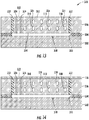
- the device layer 306 includes a second trench portion 332 etched between the passivation layer 116 and the cavity 308.
- the second trench portion 332 is etched and refilled with oxide prior to the annealing of the SOI wafer 300 ( FIG. 13 ).
- a passivation layer 116 is then deposited above the device layer 306, the spacer 324, and the oxide-filled second trench portion 332 ( FIG. 14 ).
- a plurality of vent holes (not shown) is etched through the passivation layer 116 at locations corresponding to the oxide-filled second trench portion 332.
- An HF vapor etch release is performed which releases the oxide within the second trench portion 332 to isolate a first portion 328 of the device layer 306 from a second portion 330 ( FIG. 15 ).
- a clean high temperature seal is then performed in an epi reactor to seal the vent holes.
- the SOI wafer 300 provided according to the above-described process can be further processed to form the electronic device 100 of FIGs. 1 and 2 .
- a portion of the passivation layer 116 adjacent to the side electrode is patterned to expose the side electrode 122.
- a metal layer is then deposited above the passivation layer 116 and the exposed side electrode 122.
- the metal layer is patterned to form the first metal portion 118 above the channels 110, 134 and the second metal portion 119 which contacts the side electrode 122 through the patterned portion of the passivation layer 116 for electrical communication therebetween.
- the process described above with reference to FIGs. 7-15 may be modified in a number of ways to provide additional electronic device variants such as those variants described above with reference to FIGs. 3-6 .
- the electronic device 300 of FIG. 3 is provided by etching the channel-forming trenches (340 in FIG. 8 ) through a device layer having a relatively thin thickness (compare 106 in FIG. 3 to 306 in FIG. 8 ).
- the thinner device layer 106 enables the channel-forming trenches to extend for a lesser length between the upper and the lower surfaces of the device layer 106. Accordingly, when the SOI wafer is annealed as described above with reference to FIGs. 11 and 12 , the resulting silicon migration forms a single, atomic-smooth, continuous channel 110 within the device layer 106.
- a passivation layer 116 is then deposited over the sealed device layer 106.
- FIG. 4 depicts the electronic device 300 of FIG. 3 with a first metal portion 118 patterned from a metal layer deposited above the passivation layer 116.
- FIG. 5 shows the electronic device 300 of FIG. 3 with a side electrode 122 defined within the device layer 106.
- the device layer 106 Prior to forming the first channel 110, the device layer 106 is etched to form a trench portion (325 in FIG. 7 ). The trench portion 325 is then filled with a nitride portion to form a spacer 124, which electrically isolates the side electrode 122 therein.
- the passivation layer 116 is patterned to expose a portion of the side electrode 122.
- a metal layer is deposited above the passivation layer 116 and the exposed side electrode 122.
- FIG. 6 shows the electronic device 300 of FIG. 3 with a second trench portion 132 etched through the device layer 106 in accordance with the process described with reference to FIGs. 13-14 .
- the second trench portion 132 thermally decouples the first portion 128 of the device layer 106, which includes the first channel 110, from the second portion 130.
- FIGS. 16-19 illustrate a further modification of the above described process to form an electronic device with a continuous channel having different cross sections along the channel path.
- an SOI wafer 400 including a base layer 402, a buried oxide layer 404, and a device layer 406 is etched in a similar manner as the SOI wafer 300 ( FIGs. 9 and 10 ) to define a plurality of channel-forming trenches 440 through the device layer 406 and between an upper surface 412 and a lower surface 414 of the device layer 406.
- a hydrofluoric acid (HF) vapor etch release is performed which releases a portion of the buried oxide layer 404 located proximate to the channel-forming trenches 440.
- the portion 405 of the buried oxide layer 404 not released by the HF vapor etch release remains to anchor the device layer 406 to the base layer 402.
- FIG. 17 shows a top view of the SOI wafer 400 of FIG. 16 after performance of the HF vapor etch release.
- the SOI wafer 400 in the embodiment shown in FIGs. 16 and 17 differs from the SOI wafer 300 shown in FIGs. 9 and 10 in that the wafer 400 includes at least one portion of trenches 460 arranged both one-behind-the-other and side-by-side along the channel path in the device layer 406.
- the transition from the trenches 440 to the trenches 460 is shown going from one-trench-wide to five-trenches-wide, other transition configurations are possible.
- the number of side-by-side trenches for any portion of the channel path may increase or decrease by one or more trenches at every consecutive trench position along the channel path to form a graded transition.
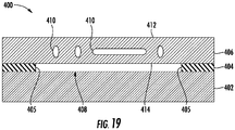
- FIGs. 18 and 19 show the SOI wafer 400 of FIGs. 16 and 17 after the wafer 400 is subjected to the annealing process as described above.
- the migration of silicon portions across all of the channel-forming trenches 440, 460 and from between all adjacent channel-forming trenches 440, 460 results in the formation of an atomic-smooth, continuous channel 410 through the device layer 406.
- the annealing process also results in the formation of a cavity 408 defined by the base layer 402, the device layer 406, and the remaining portions 405 of the buried oxide layer 404 after the annealing process.
- the annealing of SOI wafer 400 results in the channel 410 having a plate-like cross section along the portion of the channel formed from the trenches 460.
- a plate-like cross section is depicted in FIGs. 16 and 17 , other cross sectional geometries may be formed by varying one or more of the number, the spacing, the geometry, and the path of the channel-forming trenches formed in the device layer.
- the above-described processes enable the production of micro-gas-chromatographs with novel separator columns.
- the separator columns provided by the disclosed methods enable small channel cross sections and long channel lengths with atomic smooth channel sidewalls, high channel packaging density, multiple channels positioned on top of each other, and channel segments that are thermally decoupled from the substrates.
- the micro-gas-chromatographs produced according to the above-described processes enable electrostatic and thermal actuators to be positioned in close proximity to the separator columns such that the material passing through the columns can be locally heated and/or cooled and/or electrically biased.
Landscapes
- Chemical & Material Sciences (AREA)
- Engineering & Computer Science (AREA)
- Analytical Chemistry (AREA)
- General Physics & Mathematics (AREA)
- Biochemistry (AREA)
- Pathology (AREA)
- Immunology (AREA)
- Physics & Mathematics (AREA)
- Health & Medical Sciences (AREA)
- Life Sciences & Earth Sciences (AREA)
- General Health & Medical Sciences (AREA)
- Manufacturing & Machinery (AREA)
- Microelectronics & Electronic Packaging (AREA)
- Nanotechnology (AREA)
- Dispersion Chemistry (AREA)
- Computer Hardware Design (AREA)
- Micromachines (AREA)
- Other Investigation Or Analysis Of Materials By Electrical Means (AREA)
Claims (20)
- Verfahren zum Bilden einer Vorrichtung eines mikroelektromechanischen Systems (MEMS-Vorrichtung) für einen Gaschromatographen, das Folgendes umfasst:Bereitstellen eines Silizium-auf-Isolator-Wafers (SOI-Wafers) (300), der eine Grundschicht (302), eine Vorrichtungsschicht (306) über der Grundschicht (302) und eine vergrabene Oxidschicht (304) zwischen der Grundschicht (302) und einer unteren Oberfläche (314) der Vorrichtungsschicht (306) enthält;Ätzen mehrerer Gräben (340) von einer oberen Oberfläche (312) der Vorrichtungsschicht (306) zur vergrabenen Oxidschicht (304), wobei die Gräben (340) entlang eines aufeinanderfolgenden Weges in der Vorrichtungsschicht (306) beabstandet sind;Freisetzen eines Abschnitts der vergrabenen Oxidschicht (304) durch die Gräben (340); undGlühen des SOI-Wafers (300), um die Gräben (340) an der oberen und der unteren Oberfläche (312, 314) der Vorrichtungsschicht (306) abzudichten, um (i) einen oder mehrere atomar glatte, ununterbrochene Kanäle (310, 334) in der Vorrichtungsschicht (306) und (ii) einen Hohlraum (308), der durch die Grundschicht (302), die vergrabene Oxidschicht (304) und die untere Oberfläche (314) der Vorrichtungsschicht (306) begrenzt ist, zu bilden;wobei das Glühen des SOI-Wafers (300) ermöglicht, dass Abschnitte des Siliziums in der Vorrichtungsschicht (306) in der Nähe der oberen und der unteren Oberfläche (312, 314) der Vorrichtungsschicht (306) quer zu den Gräben (340) migrieren und die Gräben (340) an der oberen und der unteren Oberfläche (312, 314) abdichten;wobei die fortgesetzte Migration der Siliziumabschnitte quer zu den Gräben (340) und aus den Abschnitten zwischen benachbarten Gräben (340) die Bildung des einen oder der mehreren atomar glatten, ununterbrochenen Kanäle (310, 334) durch die Vorrichtungsschicht (306) ergibt; undwobei das Abdichten der Gräben (340) an der unteren Oberfläche (314) der Vorrichtungsschicht (306) aufgrund des Glühens des SOI-Wafers (300) außerdem den Hohlraum (308) definiert.
- Verfahren nach Anspruch 1, wobei:der eine oder die mehreren atomar glatten, ununterbrochenen Kanäle (310, 334) einen ersten ununterbrochenen Kanal (310) und einen zweiten ununterbrochenen Kanal (334) enthalten, unddie Vorrichtungsschicht (306) (i) einen ersten Eingang, der in den ersten ununterbrochenen Kanal (310) führt, und einen ersten Ausgang, der aus dem ersten ununterbrochenen Kanal (310) führt, und (ii) einen zweiten Eingang, der in den zweiten ununterbrochenen Kanal (334) führt, und einen zweiten Ausgang, der aus dem zweiten ununterbrochenen Kanal (334) führt, definiert.
- Verfahren nach Anspruch 2, wobei:der erste ununterbrochene Kanal (310) im Wesentlichen entlang einer ersten Ebene durch die Vorrichtungsschicht (306) angeordnet ist,der zweite ununterbrochene Kanal (334) im Wesentlichen entlang einer zweiten Ebene durch die Vorrichtungsschicht (306) angeordnet ist, wobei die zweite Ebene von der ersten Ebene beabstandet ist, undder erste Ausgang des ersten ununterbrochenen Kanals (310) mit dem zweiten Eingang des zweiten ununterbrochenen Kanals (334) verbunden ist, derart, dass der erste und der zweite ununterbrochene Kanal einen einzigen ununterbrochenen Kanal bilden, der durch die Vorrichtungsschicht (306) verläuft.
- Verfahren nach Anspruch 1, das ferner Folgendes umfasst:Ätzen eines Grabenabschnitts (332) von der oberen Oberfläche (312) der Vorrichtungsschicht (306) zur vergrabenen Oxidschicht (304), wobei der Grabenabschnitt (332) einen ersten Abschnitt der Vorrichtungsschicht (306), der den einen oder die mehreren atomar glatten, ununterbrochenen Kanäle (310, 334) enthält, umgibt;Befüllen des Grabenabschnitts (332) mit einem Oxid;Auftragen einer Passivierungsschicht (116) über der Vorrichtungsschicht (306) und dem mit einem Oxid gefüllten Grabenabschnitt (332);Ätzen mehrerer Lüftungslöcher durch die Passivierungsschicht (116) an Orten, die dem mit einem Oxid gefüllten Grabenabschnitt (332) entsprechen;Freisetzen des Oxids aus dem Inneren des Grabenabschnitts (332), um den ersten Abschnitt der Vorrichtungsschicht (306) von einem zweiten Abschnitt der Vorrichtungsschicht thermisch zu entkoppeln; undAbdichten der Lüftungslöcher.
- Verfahren nach Anspruch 4, wobei:das Freisetzen des Oxids aus dem Inneren des Grabenabschnitts (332) das Durchführen eines Freisetzens mittels eines Fluorwasserstoffsäuredampf-Ätzmittels (HF-Dampf-Ätzmittels) enthält, unddas Abdichten der Lüftungslöcher das Durchführen einer reinen Hochtemperaturabdichtung in einem "Epi"-Reaktor enthält.
- Verfahren nach Anspruch 1, das ferner Folgendes umfasst:Bilden eines Abstandselements (324) von der oberen Oberfläche (312) der Vorrichtungsschicht (306) zur vergrabenen Oxidschicht (304), um eine Seitenelektrode (322) in der Vorrichtungsschicht (306) elektrisch zu isolieren, vor dem Ätzen der mehreren Gräben (340), wobei das Abstandselement (324) in räumlicher Nähe zumindest zu einem Abschnitt des einen oder der mehreren atomar glatten, ununterbrochenen Kanäle (310, 334) angeordnet ist;Auftragen einer Passivierungsschicht (116) über der Vorrichtungsschicht (306), dem Abstandselement (324) und der Seitenelektrode (322);Strukturieren eines Abschnitts der Passivierungsschicht (116), um die Seitenelektrode (322) freizulegen;Auftragen einer Metallschicht über der strukturierten Passivierungsschicht (116) und der freiliegenden Seitenelektrode (322); undStrukturieren der Metallschicht, um einen Metallabschnitt zu bilden, der sich mit der Seitenelektrode (322) in elektrischer Verbindung befindet, wobei der Metallabschnitt und die Seitenelektrode (322) ein elektrostatisches Vorbelasten eines Materials, das durch den einen oder die mehreren atomar glatten, ununterbrochenen Kanäle (310, 334) befördert wird, ermöglichen.
- Verfahren nach Anspruch 1, das ferner Folgendes umfasst:Auftragen einer Passivierungsschicht (116) über der Vorrichtungsschicht (306);Auftragen einer Metallschicht über der Passivierungsschicht (116);Strukturieren der Metallschicht, um in räumlicher Nähe zu einem Abschnitt des einen oder der mehreren atomar glatten, ununterbrochenen Kanäle (310, 334) einen Metallabschnitt zu bilden,wobei der Metallabschnitt als eine obere Elektrode und/oder ein lokales Heizelement und/oder ein Seebeck-Element konfiguriert ist.
- Verfahren nach Anspruch 1, wobei der aufeinanderfolgende Weg der beabstandeten Gräben (340) eine sich wiederholende Rechteckwelle und/oder eine sich wiederholende Sinuswelle und/oder eine Dreieckswelle und/oder eine Sägezahnwelle und/oder einen mäandernden Weg durch die Vorrichtungsschicht bildet, wenn er der oberen Oberfläche (312) der Vorrichtungsschicht (306) zugewandt von oben betrachtet wird.
- Verfahren nach Anspruch 1, wobei der aufeinanderfolgendes Weg der beabstandeten Gräben (340) Gräben enthält, die (i) in einer Reihe einer nach dem anderen, ein Graben nach dem anderen Graben und/oder (ii) zwei oder mehr Gräben breit angeordnet sind, wenn er der oberen Oberfläche der Vorrichtungsschicht (306) zugewandt von oben betrachtet wird.
- Verfahren nach Anspruch 1, wobei der eine oder die mehreren atomar glatten, ununterbrochenen Kanäle (310, 334) Querschnitte aufweisen, die konstant und/oder veränderlich und/oder eine Kombination von konstanten und veränderlichen Abschnitten sind, wenn sie entlang einer Schnittebene betrachtet werden, die senkrecht zu einem Weg der Kanäle durch die Vorrichtungsschicht (306) verläuft.
- Verfahren nach Anspruch 1, wobei das Glühen des SOI-Wafers (300) das Glühen des SOI-Wafers (300):in einer reduzierenden Umgebung,bei einer hohen Temperatur höher als 1000 Grad Celsius, undfür eine Dauer von 10 Sekunden bis 10 Minuten umfasst.
- Verfahren nach Anspruch 1, wobei das Freisetzen eines Abschnitts der vergrabenen Oxidschicht (304) das Durchführen eines Freisetzens mittels eines Fluorwasserstoffsäuredampf-Ätzmittels (HF-Dampf-Ätzmittels) umfasst.
- Verfahren nach Anspruch 1, wobei das Bereitstellen eines SOI-Wafers (300) Folgendes umfasst:entweder das Bereitstellen eines SOI-Wafers (300), der eine Vorrichtungsschicht (306) mit einer dicken Schichtdicke aufweist, derart, dass das aufeinanderfolgende Glühen des SOI-Wafers (300) mindestens zwei atomar glatte, ununterbrochene Kanäle in der Vorrichtungsschicht bildet, oderdas Bereitstellen eines SOI-Wafers (300), der eine Vorrichtungsschicht mit einer dünnen Schichtdicke aufweist, derart, dass das aufeinanderfolgende Glühen des SOI-Wafers (300) einen atomar glatten, ununterbrochenen Kanal in der Vorrichtungsschicht (306) bildet.
- Vorrichtung eines mikroelektromechanischen Systems (MEMS-Vorrichtung) für einen Gaschromatographen, die Folgendes umfasst:eine Grundschicht (102);eine Vorrichtungsschicht (106), die durch einen Abschnitt einer vergrabenen Oxidschicht (104) über der Grundschicht (102) vertikal getragen wird;einen Hohlraum (108) in der vergrabenen Oxidschicht (104), der sich zwischen der Grundschicht (102) und einem freigesetzten Abschnitt der Vorrichtungsschicht (106), der durch Freisetzen eines Abschnitts der vergrabenen Oxidschicht (104) erhalten wird, horizontal erstreckt; undeine Passivierungsschicht (116), die den freigesetzten Abschnitt der Vorrichtungsschicht (106) über dem Hohlraum (108) trägt, wobei der freigesetzte Abschnitt einen oder mehrere atomar glatte, ununterbrochene Kanäle (110, 134) enthält, die sich in dem freigesetzten Abschnitt unter einer oberen Oberfläche (112) des freigesetzten Abschnitts und über einer unteren Oberfläche (114) des freigesetzten Abschnitts horizontal erstrecken.
- MEMS-Vorrichtung nach Anspruch 14, die ferner Folgendes umfasst:eine Seitenelektrode (122), die in dem freigesetzten Abschnitt der Vorrichtungsschicht (106) durch ein Abstandselement (124) definiert ist, das einen Nitridabschnitt umfasst, wobei die Seitenelektrode (122) in räumlicher Nähe zu einem Abschnitt des einen oder der mehreren atomar glatten, ununterbrochenen Kanäle (110, 134) angeordnet ist; undeinen Metallabschnitt (119), der sich durch einen Abschnitt der Passivierungsschicht (116) erstreckt, derart, dass sich der Metallabschnitt (119) mit der Seitenelektrode (122) in elektrischer Verbindung befindet.
- MEMS-Vorrichtung nach Anspruch 14, die ferner Folgendes umfasst:
einen Grabenabschnitt (132), der sich zwischen der Passivierungsschicht (116) und dem Hohlraum (108) erstreckt, wobei der Grabenabschnitt (132) den freigesetzten Abschnitt der Vorrichtungsschicht (106) umgibt, derart, dass der Grabenabschnitt (132) und der Hohlraum (108) den freigesetzten Abschnitt von einem nicht freigesetzten Abschnitt der Vorrichtungsschicht (106) thermisch entkoppeln. - MEMS-Vorrichtung nach Anspruch 14, wobei:der eine oder die mehreren atomar glatten, ununterbrochenen Kanäle (110, 134) einen ersten Kanal (110) und einen zweiten Kanal (134) enthalten, undder freigesetzte Abschnitt der Vorrichtungsschicht (106) (i) einen ersten Eingang, der in den ersten Kanal (110) führt, und einen ersten Ausgang, der aus dem ersten Kanal (110) führt, und (ii) einen zweiten Eingang, der in den zweiten Kanal (134) führt, und einen zweiten Ausgang, der aus dem zweiten Kanal (134) führt, definiert.
- MEMS-Vorrichtung nach Anspruch 17, wobei:der erste Kanal (110) im Wesentlichen entlang einer ersten Ebene durch den freigesetzten Abschnitt der Vorrichtungsschicht (106) angeordnet ist, undder zweite Kanal (134) im Wesentlichen entlang einer zweiten Ebene durch den freigesetzten Abschnitt der Vorrichtungsschicht (106) angeordnet ist, wobei die zweite Ebene von der ersten Ebene beabstandet ist.
- MEMS-Vorrichtung nach Anspruch 17, wobei der erste und der zweite Kanal (110, 134) im Wesentlichen entlang einer gemeinsamen Ebene durch den freigesetzten Abschnitt der Vorrichtungsschicht (106) angeordnet sind.
- MEMS-Vorrichtung nach Anspruch 14, wobei:die Vorrichtungsschicht (106) eine Schicht entweder aus mono- oder polykristallinem Silizium ist, die eine Dicke von etwa 5 bis 50 µm aufweist, unddie vergrabene Oxidschicht (104) eine Dicke von etwa 0,5 bis 2,5 µm aufweist.
Applications Claiming Priority (2)
| Application Number | Priority Date | Filing Date | Title |
|---|---|---|---|
| US201462093047P | 2014-12-17 | 2014-12-17 | |
| PCT/US2015/066076 WO2016100504A2 (en) | 2014-12-17 | 2015-12-16 | A mems gas chromatograph and method of forming a separator column for a mems gas chromatograph |
Publications (3)
| Publication Number | Publication Date |
|---|---|
| EP3234589A2 EP3234589A2 (de) | 2017-10-25 |
| EP3234589A4 EP3234589A4 (de) | 2018-08-15 |
| EP3234589B1 true EP3234589B1 (de) | 2020-04-15 |
Family
ID=56127844
Family Applications (1)
| Application Number | Title | Priority Date | Filing Date |
|---|---|---|---|
| EP15870978.2A Active EP3234589B1 (de) | 2014-12-17 | 2015-12-16 | Mems-gaschromatograph und verfahren zur formung einer separatorsäule für einen mems-gaschromatographen |
Country Status (3)
| Country | Link |
|---|---|
| US (1) | US10060888B2 (de) |
| EP (1) | EP3234589B1 (de) |
| WO (1) | WO2016100504A2 (de) |
Families Citing this family (5)
| Publication number | Priority date | Publication date | Assignee | Title |
|---|---|---|---|---|
| CN107285269A (zh) * | 2017-06-23 | 2017-10-24 | 中国科学院苏州纳米技术与纳米仿生研究所 | 微机电系统器件及其制备方法 |
| CN108151735B (zh) * | 2017-12-08 | 2020-05-19 | 华中科技大学 | 一种利用soi片制作高精度mems惯性传感器的方法 |
| CN109962067B (zh) * | 2017-12-22 | 2023-12-29 | 中国科学院上海微系统与信息技术研究所 | 基于soi的微色谱柱及微热导检测器的集成芯片及制备方法 |
| CN112368234B (zh) * | 2019-04-03 | 2023-11-21 | 京东方科技集团股份有限公司 | 微纳米通道结构、传感器及其制备方法、微流体装置 |
| CN114684772B (zh) * | 2020-12-31 | 2025-07-04 | 中芯集成电路(宁波)有限公司 | 半导体器件及其制作方法 |
Family Cites Families (8)
| Publication number | Priority date | Publication date | Assignee | Title |
|---|---|---|---|---|
| JP4074051B2 (ja) * | 1999-08-31 | 2008-04-09 | 株式会社東芝 | 半導体基板およびその製造方法 |
| WO2007082745A1 (en) * | 2006-01-18 | 2007-07-26 | Universite Catholique De Louvain | Selective etching for semiconductor devices |
| US7563633B2 (en) | 2006-08-25 | 2009-07-21 | Robert Bosch Gmbh | Microelectromechanical systems encapsulation process |
| EP2256084B1 (de) * | 2009-05-27 | 2012-07-11 | Nxp B.V. | Verfahren zur Herstellung eines MEMS-Elementes |
| WO2011154363A2 (en) * | 2010-06-07 | 2011-12-15 | Commissariat à l'énergie atomique et aux énergies alternatives | Analysis device including a mems and/or nems network |
| US8343789B2 (en) * | 2010-08-17 | 2013-01-01 | Taiwan Semiconductor Manufacturing Company, Ltd. | Microstructure device with an improved anchor |
| AU2013222069A1 (en) * | 2012-02-26 | 2014-10-16 | Solexel, Inc. | Systems and methods for laser splitting and device layer transfer |
| US8940639B2 (en) * | 2012-12-18 | 2015-01-27 | Analog Devices, Inc. | Methods and structures for using diamond in the production of MEMS |
-
2015
- 2015-12-16 WO PCT/US2015/066076 patent/WO2016100504A2/en not_active Ceased
- 2015-12-16 US US15/535,522 patent/US10060888B2/en active Active
- 2015-12-16 EP EP15870978.2A patent/EP3234589B1/de active Active
Non-Patent Citations (1)
| Title |
|---|
| None * |
Also Published As
| Publication number | Publication date |
|---|---|
| US10060888B2 (en) | 2018-08-28 |
| EP3234589A4 (de) | 2018-08-15 |
| US20170363588A1 (en) | 2017-12-21 |
| WO2016100504A2 (en) | 2016-06-23 |
| WO2016100504A3 (en) | 2016-08-11 |
| EP3234589A2 (de) | 2017-10-25 |
Similar Documents
| Publication | Publication Date | Title |
|---|---|---|
| US10060888B2 (en) | MEMS gas chromatograph and method of forming a separator column for a MEMS gas chromatograph | |
| US9102519B2 (en) | Semiconductor devices and methods of forming thereof | |
| US7678600B2 (en) | Process for manufacturing a membrane of semiconductor material integrated in, and electrically insulated from, a substrate | |
| CN101119924B (zh) | 带有双膜片的微机械膜片传感器 | |
| US8481400B2 (en) | Semiconductor manufacturing and semiconductor device with semiconductor structure | |
| US8994127B2 (en) | Method of fabricating isolating semiconductor structures using a layout of trenches and openings | |
| KR101892776B1 (ko) | 면외 이격체로 형성된 전극 | |
| JP2017052092A (ja) | 変更した応力特性を有する薄膜を形成する方法 | |
| US9783407B2 (en) | Method for making a suspended membrane structure with buried electrode | |
| US9643836B2 (en) | Method for producing a pressure sensor and corresponding sensor | |
| US8759136B2 (en) | Method for creating monocrystalline piezoresistors | |
| KR20070046087A (ko) | 기판상의 층을 에칭하기 위한 방법 | |
| US8138556B2 (en) | Pre-released structure device | |
| TWI616394B (zh) | 增強之微機電系統裝置及其製造方法 | |
| US8470184B2 (en) | Method for making a cavity in the thickness of a substrate which may form a site for receiving a component | |
| JP2014120729A (ja) | 半導体基板の製造方法および半導体装置 | |
| US9114975B2 (en) | Micromechanical component and method for producing a micromechanical component having a thin-layer cap | |
| US10585074B2 (en) | Method of fabricating a MEMS and/or NEMS structure comprising at least two elements suspended from a support at different distances from said support | |
| US8430255B2 (en) | Method of accurately spacing Z-axis electrode | |
| US10370240B2 (en) | Layer structure and method of manufacturing a layer structure | |
| US12503361B2 (en) | MEMS sensor and method of manufacturing MEMS sensor | |
| KR20140022881A (ko) | 매입형 플러그를 갖춘 웨이퍼 | |
| CN119731116A (zh) | 用于制造具有电连接部的硅层系统的方法 | |
| JP2018096938A (ja) | 半導体デバイス、およびその製造方法 | |
| JP2010097833A (ja) | 基板を貫通してマイクロ電気機械デバイスに至る電気接続部 |
Legal Events
| Date | Code | Title | Description |
|---|---|---|---|
| STAA | Information on the status of an ep patent application or granted ep patent |
Free format text: STATUS: THE INTERNATIONAL PUBLICATION HAS BEEN MADE |
|
| PUAI | Public reference made under article 153(3) epc to a published international application that has entered the european phase |
Free format text: ORIGINAL CODE: 0009012 |
|
| STAA | Information on the status of an ep patent application or granted ep patent |
Free format text: STATUS: REQUEST FOR EXAMINATION WAS MADE |
|
| 17P | Request for examination filed |
Effective date: 20170717 |
|
| AK | Designated contracting states |
Kind code of ref document: A2 Designated state(s): AL AT BE BG CH CY CZ DE DK EE ES FI FR GB GR HR HU IE IS IT LI LT LU LV MC MK MT NL NO PL PT RO RS SE SI SK SM TR |
|
| AX | Request for extension of the european patent |
Extension state: BA ME |
|
| RIN1 | Information on inventor provided before grant (corrected) |
Inventor name: KIM, BONGSANG Inventor name: STEHLE, JOCHEN Inventor name: O'BRIEN, GARY Inventor name: FEYN, ANDO |
|
| DAV | Request for validation of the european patent (deleted) | ||
| DAX | Request for extension of the european patent (deleted) | ||
| A4 | Supplementary search report drawn up and despatched |
Effective date: 20180716 |
|
| RIC1 | Information provided on ipc code assigned before grant |
Ipc: H01L 21/77 20170101ALN20180710BHEP Ipc: B81C 1/00 20060101ALI20180710BHEP Ipc: G01N 30/60 20060101AFI20180710BHEP Ipc: B81B 7/00 20060101ALI20180710BHEP |
|
| GRAP | Despatch of communication of intention to grant a patent |
Free format text: ORIGINAL CODE: EPIDOSNIGR1 |
|
| STAA | Information on the status of an ep patent application or granted ep patent |
Free format text: STATUS: GRANT OF PATENT IS INTENDED |
|
| RIC1 | Information provided on ipc code assigned before grant |
Ipc: B81C 1/00 20060101ALI20191016BHEP Ipc: B81B 7/00 20060101ALI20191016BHEP Ipc: G01N 30/60 20060101AFI20191016BHEP Ipc: H01L 21/77 20170101ALN20191016BHEP |
|
| INTG | Intention to grant announced |
Effective date: 20191108 |
|
| RIN1 | Information on inventor provided before grant (corrected) |
Inventor name: O'BRIEN, GARY Inventor name: FEYN, ANDO Inventor name: STEHLE, JOCHEN Inventor name: KIM, BONGSANG |
|
| GRAS | Grant fee paid |
Free format text: ORIGINAL CODE: EPIDOSNIGR3 |
|
| GRAA | (expected) grant |
Free format text: ORIGINAL CODE: 0009210 |
|
| STAA | Information on the status of an ep patent application or granted ep patent |
Free format text: STATUS: THE PATENT HAS BEEN GRANTED |
|
| AK | Designated contracting states |
Kind code of ref document: B1 Designated state(s): AL AT BE BG CH CY CZ DE DK EE ES FI FR GB GR HR HU IE IS IT LI LT LU LV MC MK MT NL NO PL PT RO RS SE SI SK SM TR |
|
| REG | Reference to a national code |
Ref country code: CH Ref legal event code: EP |
|
| RAP2 | Party data changed (patent owner data changed or rights of a patent transferred) |
Owner name: ROBERT BOSCH GMBH |
|
| REG | Reference to a national code |
Ref country code: DE Ref legal event code: R096 Ref document number: 602015050907 Country of ref document: DE |
|
| REG | Reference to a national code |
Ref country code: IE Ref legal event code: FG4D |
|
| REG | Reference to a national code |
Ref country code: AT Ref legal event code: REF Ref document number: 1257924 Country of ref document: AT Kind code of ref document: T Effective date: 20200515 |
|
| REG | Reference to a national code |
Ref country code: NL Ref legal event code: MP Effective date: 20200415 |
|
| REG | Reference to a national code |
Ref country code: LT Ref legal event code: MG4D |
|
| PG25 | Lapsed in a contracting state [announced via postgrant information from national office to epo] |
Ref country code: PT Free format text: LAPSE BECAUSE OF FAILURE TO SUBMIT A TRANSLATION OF THE DESCRIPTION OR TO PAY THE FEE WITHIN THE PRESCRIBED TIME-LIMIT Effective date: 20200817 Ref country code: FI Free format text: LAPSE BECAUSE OF FAILURE TO SUBMIT A TRANSLATION OF THE DESCRIPTION OR TO PAY THE FEE WITHIN THE PRESCRIBED TIME-LIMIT Effective date: 20200415 Ref country code: IS Free format text: LAPSE BECAUSE OF FAILURE TO SUBMIT A TRANSLATION OF THE DESCRIPTION OR TO PAY THE FEE WITHIN THE PRESCRIBED TIME-LIMIT Effective date: 20200815 Ref country code: GR Free format text: LAPSE BECAUSE OF FAILURE TO SUBMIT A TRANSLATION OF THE DESCRIPTION OR TO PAY THE FEE WITHIN THE PRESCRIBED TIME-LIMIT Effective date: 20200716 Ref country code: NO Free format text: LAPSE BECAUSE OF FAILURE TO SUBMIT A TRANSLATION OF THE DESCRIPTION OR TO PAY THE FEE WITHIN THE PRESCRIBED TIME-LIMIT Effective date: 20200715 Ref country code: LT Free format text: LAPSE BECAUSE OF FAILURE TO SUBMIT A TRANSLATION OF THE DESCRIPTION OR TO PAY THE FEE WITHIN THE PRESCRIBED TIME-LIMIT Effective date: 20200415 Ref country code: SE Free format text: LAPSE BECAUSE OF FAILURE TO SUBMIT A TRANSLATION OF THE DESCRIPTION OR TO PAY THE FEE WITHIN THE PRESCRIBED TIME-LIMIT Effective date: 20200415 Ref country code: NL Free format text: LAPSE BECAUSE OF FAILURE TO SUBMIT A TRANSLATION OF THE DESCRIPTION OR TO PAY THE FEE WITHIN THE PRESCRIBED TIME-LIMIT Effective date: 20200415 |
|
| REG | Reference to a national code |
Ref country code: AT Ref legal event code: MK05 Ref document number: 1257924 Country of ref document: AT Kind code of ref document: T Effective date: 20200415 |
|
| PG25 | Lapsed in a contracting state [announced via postgrant information from national office to epo] |
Ref country code: RS Free format text: LAPSE BECAUSE OF FAILURE TO SUBMIT A TRANSLATION OF THE DESCRIPTION OR TO PAY THE FEE WITHIN THE PRESCRIBED TIME-LIMIT Effective date: 20200415 Ref country code: BG Free format text: LAPSE BECAUSE OF FAILURE TO SUBMIT A TRANSLATION OF THE DESCRIPTION OR TO PAY THE FEE WITHIN THE PRESCRIBED TIME-LIMIT Effective date: 20200715 Ref country code: HR Free format text: LAPSE BECAUSE OF FAILURE TO SUBMIT A TRANSLATION OF THE DESCRIPTION OR TO PAY THE FEE WITHIN THE PRESCRIBED TIME-LIMIT Effective date: 20200415 Ref country code: LV Free format text: LAPSE BECAUSE OF FAILURE TO SUBMIT A TRANSLATION OF THE DESCRIPTION OR TO PAY THE FEE WITHIN THE PRESCRIBED TIME-LIMIT Effective date: 20200415 |
|
| PG25 | Lapsed in a contracting state [announced via postgrant information from national office to epo] |
Ref country code: AL Free format text: LAPSE BECAUSE OF FAILURE TO SUBMIT A TRANSLATION OF THE DESCRIPTION OR TO PAY THE FEE WITHIN THE PRESCRIBED TIME-LIMIT Effective date: 20200415 |
|
| REG | Reference to a national code |
Ref country code: DE Ref legal event code: R097 Ref document number: 602015050907 Country of ref document: DE |
|
| PG25 | Lapsed in a contracting state [announced via postgrant information from national office to epo] |
Ref country code: SM Free format text: LAPSE BECAUSE OF FAILURE TO SUBMIT A TRANSLATION OF THE DESCRIPTION OR TO PAY THE FEE WITHIN THE PRESCRIBED TIME-LIMIT Effective date: 20200415 Ref country code: EE Free format text: LAPSE BECAUSE OF FAILURE TO SUBMIT A TRANSLATION OF THE DESCRIPTION OR TO PAY THE FEE WITHIN THE PRESCRIBED TIME-LIMIT Effective date: 20200415 Ref country code: ES Free format text: LAPSE BECAUSE OF FAILURE TO SUBMIT A TRANSLATION OF THE DESCRIPTION OR TO PAY THE FEE WITHIN THE PRESCRIBED TIME-LIMIT Effective date: 20200415 Ref country code: DK Free format text: LAPSE BECAUSE OF FAILURE TO SUBMIT A TRANSLATION OF THE DESCRIPTION OR TO PAY THE FEE WITHIN THE PRESCRIBED TIME-LIMIT Effective date: 20200415 Ref country code: AT Free format text: LAPSE BECAUSE OF FAILURE TO SUBMIT A TRANSLATION OF THE DESCRIPTION OR TO PAY THE FEE WITHIN THE PRESCRIBED TIME-LIMIT Effective date: 20200415 Ref country code: IT Free format text: LAPSE BECAUSE OF FAILURE TO SUBMIT A TRANSLATION OF THE DESCRIPTION OR TO PAY THE FEE WITHIN THE PRESCRIBED TIME-LIMIT Effective date: 20200415 Ref country code: CZ Free format text: LAPSE BECAUSE OF FAILURE TO SUBMIT A TRANSLATION OF THE DESCRIPTION OR TO PAY THE FEE WITHIN THE PRESCRIBED TIME-LIMIT Effective date: 20200415 Ref country code: RO Free format text: LAPSE BECAUSE OF FAILURE TO SUBMIT A TRANSLATION OF THE DESCRIPTION OR TO PAY THE FEE WITHIN THE PRESCRIBED TIME-LIMIT Effective date: 20200415 |
|
| PLBE | No opposition filed within time limit |
Free format text: ORIGINAL CODE: 0009261 |
|
| STAA | Information on the status of an ep patent application or granted ep patent |
Free format text: STATUS: NO OPPOSITION FILED WITHIN TIME LIMIT |
|
| PG25 | Lapsed in a contracting state [announced via postgrant information from national office to epo] |
Ref country code: PL Free format text: LAPSE BECAUSE OF FAILURE TO SUBMIT A TRANSLATION OF THE DESCRIPTION OR TO PAY THE FEE WITHIN THE PRESCRIBED TIME-LIMIT Effective date: 20200415 Ref country code: SK Free format text: LAPSE BECAUSE OF FAILURE TO SUBMIT A TRANSLATION OF THE DESCRIPTION OR TO PAY THE FEE WITHIN THE PRESCRIBED TIME-LIMIT Effective date: 20200415 |
|
| 26N | No opposition filed |
Effective date: 20210118 |
|
| PG25 | Lapsed in a contracting state [announced via postgrant information from national office to epo] |
Ref country code: SI Free format text: LAPSE BECAUSE OF FAILURE TO SUBMIT A TRANSLATION OF THE DESCRIPTION OR TO PAY THE FEE WITHIN THE PRESCRIBED TIME-LIMIT Effective date: 20200415 |
|
| REG | Reference to a national code |
Ref country code: CH Ref legal event code: PL |
|
| PG25 | Lapsed in a contracting state [announced via postgrant information from national office to epo] |
Ref country code: MC Free format text: LAPSE BECAUSE OF FAILURE TO SUBMIT A TRANSLATION OF THE DESCRIPTION OR TO PAY THE FEE WITHIN THE PRESCRIBED TIME-LIMIT Effective date: 20200415 |
|
| REG | Reference to a national code |
Ref country code: BE Ref legal event code: MM Effective date: 20201231 |
|
| PG25 | Lapsed in a contracting state [announced via postgrant information from national office to epo] |
Ref country code: IE Free format text: LAPSE BECAUSE OF NON-PAYMENT OF DUE FEES Effective date: 20201216 Ref country code: LU Free format text: LAPSE BECAUSE OF NON-PAYMENT OF DUE FEES Effective date: 20201216 |
|
| PG25 | Lapsed in a contracting state [announced via postgrant information from national office to epo] |
Ref country code: CH Free format text: LAPSE BECAUSE OF NON-PAYMENT OF DUE FEES Effective date: 20201231 Ref country code: LI Free format text: LAPSE BECAUSE OF NON-PAYMENT OF DUE FEES Effective date: 20201231 |
|
| PG25 | Lapsed in a contracting state [announced via postgrant information from national office to epo] |
Ref country code: TR Free format text: LAPSE BECAUSE OF FAILURE TO SUBMIT A TRANSLATION OF THE DESCRIPTION OR TO PAY THE FEE WITHIN THE PRESCRIBED TIME-LIMIT Effective date: 20200415 Ref country code: MT Free format text: LAPSE BECAUSE OF FAILURE TO SUBMIT A TRANSLATION OF THE DESCRIPTION OR TO PAY THE FEE WITHIN THE PRESCRIBED TIME-LIMIT Effective date: 20200415 Ref country code: CY Free format text: LAPSE BECAUSE OF FAILURE TO SUBMIT A TRANSLATION OF THE DESCRIPTION OR TO PAY THE FEE WITHIN THE PRESCRIBED TIME-LIMIT Effective date: 20200415 |
|
| PG25 | Lapsed in a contracting state [announced via postgrant information from national office to epo] |
Ref country code: MK Free format text: LAPSE BECAUSE OF FAILURE TO SUBMIT A TRANSLATION OF THE DESCRIPTION OR TO PAY THE FEE WITHIN THE PRESCRIBED TIME-LIMIT Effective date: 20200415 |
|
| PG25 | Lapsed in a contracting state [announced via postgrant information from national office to epo] |
Ref country code: BE Free format text: LAPSE BECAUSE OF NON-PAYMENT OF DUE FEES Effective date: 20201231 |
|
| PGFP | Annual fee paid to national office [announced via postgrant information from national office to epo] |
Ref country code: DE Payment date: 20250224 Year of fee payment: 10 |
|
| PGFP | Annual fee paid to national office [announced via postgrant information from national office to epo] |
Ref country code: GB Payment date: 20251218 Year of fee payment: 11 |
|
| PGFP | Annual fee paid to national office [announced via postgrant information from national office to epo] |
Ref country code: FR Payment date: 20251217 Year of fee payment: 11 |