EP3232468A1 - Heat dissipation structure of semiconductor device - Google Patents
Heat dissipation structure of semiconductor device Download PDFInfo
- Publication number
- EP3232468A1 EP3232468A1 EP17151972.1A EP17151972A EP3232468A1 EP 3232468 A1 EP3232468 A1 EP 3232468A1 EP 17151972 A EP17151972 A EP 17151972A EP 3232468 A1 EP3232468 A1 EP 3232468A1
- Authority
- EP
- European Patent Office
- Prior art keywords
- heat dissipation
- semiconductor device
- heat
- dissipation structure
- thermal conductivity
- Prior art date
- Legal status (The legal status is an assumption and is not a legal conclusion. Google has not performed a legal analysis and makes no representation as to the accuracy of the status listed.)
- Granted
Links
Images
Classifications
-
- H—ELECTRICITY
- H10—SEMICONDUCTOR DEVICES; ELECTRIC SOLID-STATE DEVICES NOT OTHERWISE PROVIDED FOR
- H10W—GENERIC PACKAGES, INTERCONNECTIONS, CONNECTORS OR OTHER CONSTRUCTIONAL DETAILS OF DEVICES COVERED BY CLASS H10
- H10W40/00—Arrangements for thermal protection or thermal control
- H10W40/20—Arrangements for cooling
- H10W40/22—Arrangements for cooling characterised by their shape, e.g. having conical or cylindrical projections
-
- H—ELECTRICITY
- H10—SEMICONDUCTOR DEVICES; ELECTRIC SOLID-STATE DEVICES NOT OTHERWISE PROVIDED FOR
- H10W—GENERIC PACKAGES, INTERCONNECTIONS, CONNECTORS OR OTHER CONSTRUCTIONAL DETAILS OF DEVICES COVERED BY CLASS H10
- H10W40/00—Arrangements for thermal protection or thermal control
- H10W40/20—Arrangements for cooling
- H10W40/22—Arrangements for cooling characterised by their shape, e.g. having conical or cylindrical projections
- H10W40/226—Arrangements for cooling characterised by their shape, e.g. having conical or cylindrical projections characterised by projecting parts, e.g. fins to increase surface area
- H10W40/228—Arrangements for cooling characterised by their shape, e.g. having conical or cylindrical projections characterised by projecting parts, e.g. fins to increase surface area the projecting parts being wire-shaped or pin-shaped
-
- H—ELECTRICITY
- H10—SEMICONDUCTOR DEVICES; ELECTRIC SOLID-STATE DEVICES NOT OTHERWISE PROVIDED FOR
- H10W—GENERIC PACKAGES, INTERCONNECTIONS, CONNECTORS OR OTHER CONSTRUCTIONAL DETAILS OF DEVICES COVERED BY CLASS H10
- H10W40/00—Arrangements for thermal protection or thermal control
- H10W40/20—Arrangements for cooling
- H10W40/22—Arrangements for cooling characterised by their shape, e.g. having conical or cylindrical projections
- H10W40/226—Arrangements for cooling characterised by their shape, e.g. having conical or cylindrical projections characterised by projecting parts, e.g. fins to increase surface area
-
- H—ELECTRICITY
- H10—SEMICONDUCTOR DEVICES; ELECTRIC SOLID-STATE DEVICES NOT OTHERWISE PROVIDED FOR
- H10W—GENERIC PACKAGES, INTERCONNECTIONS, CONNECTORS OR OTHER CONSTRUCTIONAL DETAILS OF DEVICES COVERED BY CLASS H10
- H10W40/00—Arrangements for thermal protection or thermal control
- H10W40/20—Arrangements for cooling
- H10W40/231—Arrangements for cooling characterised by their places of attachment or cooling paths
-
- H—ELECTRICITY
- H10—SEMICONDUCTOR DEVICES; ELECTRIC SOLID-STATE DEVICES NOT OTHERWISE PROVIDED FOR
- H10W—GENERIC PACKAGES, INTERCONNECTIONS, CONNECTORS OR OTHER CONSTRUCTIONAL DETAILS OF DEVICES COVERED BY CLASS H10
- H10W40/00—Arrangements for thermal protection or thermal control
- H10W40/20—Arrangements for cooling
- H10W40/231—Arrangements for cooling characterised by their places of attachment or cooling paths
- H10W40/235—Arrangements for cooling characterised by their places of attachment or cooling paths attached to package parts
-
- H—ELECTRICITY
- H10—SEMICONDUCTOR DEVICES; ELECTRIC SOLID-STATE DEVICES NOT OTHERWISE PROVIDED FOR
- H10W—GENERIC PACKAGES, INTERCONNECTIONS, CONNECTORS OR OTHER CONSTRUCTIONAL DETAILS OF DEVICES COVERED BY CLASS H10
- H10W40/00—Arrangements for thermal protection or thermal control
- H10W40/60—Securing means for detachable heating or cooling arrangements, e.g. clamps
- H10W40/611—Bolts or screws
-
- H—ELECTRICITY
- H10—SEMICONDUCTOR DEVICES; ELECTRIC SOLID-STATE DEVICES NOT OTHERWISE PROVIDED FOR
- H10W—GENERIC PACKAGES, INTERCONNECTIONS, CONNECTORS OR OTHER CONSTRUCTIONAL DETAILS OF DEVICES COVERED BY CLASS H10
- H10W40/00—Arrangements for thermal protection or thermal control
- H10W40/70—Fillings or auxiliary members in containers or in encapsulations for thermal protection or control
- H10W40/77—Auxiliary members characterised by their shape
-
- H—ELECTRICITY
- H10—SEMICONDUCTOR DEVICES; ELECTRIC SOLID-STATE DEVICES NOT OTHERWISE PROVIDED FOR
- H10W—GENERIC PACKAGES, INTERCONNECTIONS, CONNECTORS OR OTHER CONSTRUCTIONAL DETAILS OF DEVICES COVERED BY CLASS H10
- H10W70/00—Package substrates; Interposers; Redistribution layers [RDL]
- H10W70/60—Insulating or insulated package substrates; Interposers; Redistribution layers
- H10W70/62—Insulating or insulated package substrates; Interposers; Redistribution layers characterised by their interconnections
- H10W70/63—Vias, e.g. via plugs
- H10W70/635—Through-vias
-
- H—ELECTRICITY
- H10—SEMICONDUCTOR DEVICES; ELECTRIC SOLID-STATE DEVICES NOT OTHERWISE PROVIDED FOR
- H10W—GENERIC PACKAGES, INTERCONNECTIONS, CONNECTORS OR OTHER CONSTRUCTIONAL DETAILS OF DEVICES COVERED BY CLASS H10
- H10W70/00—Package substrates; Interposers; Redistribution layers [RDL]
- H10W70/60—Insulating or insulated package substrates; Interposers; Redistribution layers
- H10W70/62—Insulating or insulated package substrates; Interposers; Redistribution layers characterised by their interconnections
- H10W70/65—Shapes or dispositions of interconnections
-
- H—ELECTRICITY
- H10—SEMICONDUCTOR DEVICES; ELECTRIC SOLID-STATE DEVICES NOT OTHERWISE PROVIDED FOR
- H10W—GENERIC PACKAGES, INTERCONNECTIONS, CONNECTORS OR OTHER CONSTRUCTIONAL DETAILS OF DEVICES COVERED BY CLASS H10
- H10W74/00—Encapsulations, e.g. protective coatings
- H10W74/10—Encapsulations, e.g. protective coatings characterised by their shape or disposition
- H10W74/111—Encapsulations, e.g. protective coatings characterised by their shape or disposition the semiconductor body being completely enclosed
- H10W74/129—Encapsulations, e.g. protective coatings characterised by their shape or disposition the semiconductor body being completely enclosed forming a chip-scale package [CSP]
-
- H—ELECTRICITY
- H10—SEMICONDUCTOR DEVICES; ELECTRIC SOLID-STATE DEVICES NOT OTHERWISE PROVIDED FOR
- H10W—GENERIC PACKAGES, INTERCONNECTIONS, CONNECTORS OR OTHER CONSTRUCTIONAL DETAILS OF DEVICES COVERED BY CLASS H10
- H10W40/00—Arrangements for thermal protection or thermal control
- H10W40/20—Arrangements for cooling
- H10W40/231—Arrangements for cooling characterised by their places of attachment or cooling paths
- H10W40/242—Arrangements for cooling characterised by their places of attachment or cooling paths comprising thermal conductors between chips and the and the arrangements for cooling, e.g. compliant heat-spreaders
-
- H—ELECTRICITY
- H10—SEMICONDUCTOR DEVICES; ELECTRIC SOLID-STATE DEVICES NOT OTHERWISE PROVIDED FOR
- H10W—GENERIC PACKAGES, INTERCONNECTIONS, CONNECTORS OR OTHER CONSTRUCTIONAL DETAILS OF DEVICES COVERED BY CLASS H10
- H10W40/00—Arrangements for thermal protection or thermal control
- H10W40/60—Securing means for detachable heating or cooling arrangements, e.g. clamps
-
- H—ELECTRICITY
- H10—SEMICONDUCTOR DEVICES; ELECTRIC SOLID-STATE DEVICES NOT OTHERWISE PROVIDED FOR
- H10W—GENERIC PACKAGES, INTERCONNECTIONS, CONNECTORS OR OTHER CONSTRUCTIONAL DETAILS OF DEVICES COVERED BY CLASS H10
- H10W72/00—Interconnections or connectors in packages
- H10W72/071—Connecting or disconnecting
- H10W72/073—Connecting or disconnecting of die-attach connectors
- H10W72/07331—Connecting techniques
-
- H—ELECTRICITY
- H10—SEMICONDUCTOR DEVICES; ELECTRIC SOLID-STATE DEVICES NOT OTHERWISE PROVIDED FOR
- H10W—GENERIC PACKAGES, INTERCONNECTIONS, CONNECTORS OR OTHER CONSTRUCTIONAL DETAILS OF DEVICES COVERED BY CLASS H10
- H10W90/00—Package configurations
- H10W90/701—Package configurations characterised by the relative positions of pads or connectors relative to package parts
- H10W90/731—Package configurations characterised by the relative positions of pads or connectors relative to package parts of die-attach connectors
- H10W90/734—Package configurations characterised by the relative positions of pads or connectors relative to package parts of die-attach connectors between a chip and a stacked insulating package substrate, interposer or RDL
Definitions
- the present invention relates to a heat dissipation structure (also referred to as cooling structure) of a surface-mount semiconductor device, in particular, to a heat dissipation structure with heat dissipation and insulating reliability applicable to thin packaged semiconductor device.
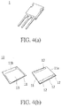
- Fig. 4(a) is a general stereogram of a lead type discrete part 1 of the prior art
- Fig. 4(b) is a general stereogram of a surface-mount semiconductor device 10 developed in recent years.
- Such a semiconductor device 10, as shown in Fig. 4(b) is received in an ultrathin package 11, for example, it includes: an electric bonding surface 11a provided with more than one electrode (terminal) 12 electrically connected with a substrate; and a heat dissipation surface 11b, wherein a large heat dissipation electrode 13 is provided on an opposite side of the electric bonding surface 11a.
- an electric bonding surface 11a provided with more than one electrode (terminal) 12 electrically connected with a substrate
- a heat dissipation surface 11b wherein a large heat dissipation electrode 13 is provided on an opposite side of the electric bonding surface 11a.
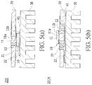
- Fig. 5(a) is a general sectional view of a heat dissipation structure 201 of the prior art
- Fig. 5(b) is a general sectional view of a heat dissipation structure 201A as the varying example.
- a semiconductor device 10 is carried via an insulated part 41 in a manner of bonding or contacting the heat dissipation surface 11b downwards, and an electrode 12 of the electric bonding surface 11a is welded to a lower surface pattern 22 of the substrate 20.
- heat produced by the semiconductor device 10 is transferred to the heat sink 30 from the heat dissipation surface 11b via the insulated part 41.
- the lower surface pattern 22 of the substrate 20 is contacted onto the heat sink 30 via the insulated part 41, and an upper surface pattern 21 of the substrate 20 and the electrode 12 of the electric bonding surface 11a of the semiconductor device 10 are welded together.
- heat produced by the semiconductor device 10 is transferred to the heat sink 30 from the electrode 12 of the electric bonding surface 11a via a thermal via or inlay disposed on the substrate 20 and the insulated part 41.
- the heat dissipation structures 201 and 201A have the following problems, but problem 1) has to be eliminated at first, that is, a thermal resistor between the semiconductor device 10 and the heat sink 30 as a heating element becomes minimum. Then, preferably, problem 2) to problem 4) can also be eliminated.
- the present invention is directed to a heat dissipation structure of a semiconductor device with excellent heat dissipation applicable to surface-mount thin semiconductor devices, and preferably, a heat dissipation structure of a semiconductor device also with excellent insulating reliability is provided.
- the semiconductor device has an electric bonding surface electrically connected with a substrate and a heat dissipation surface on an opposite side thereof, wherein the heat dissipation surface is bonded or contacted to a conductive member with high thermal conductivity via a non-insulated member, and the conductive member with high thermal conductivity is bonded or contacted to a heat dissipation part via a first insulated member.
- the thickness of the conductive member with high thermal conductivity is greater than that of the semiconductor device, the conductive member with high thermal conductivity, in a top view, is less than the heat dissipation part, and in a situation where the semiconductor device and the conductive member with high thermal conductivity, for example, are both set as a substantially rectangular shape in a top view, the length of each side of the conductive member with high thermal conductivity is greater than the sum of twice the thickness of the conductive member with high thermal conductivity and the length of each side of the semiconductor device.
- the conductive member with high thermal conductivity in a top view, is not limited to the substantially rectangular shape, for example, it may also be a substantially round shape, as long as the size thereof is determined according to the substantially rectangular shape.
- the first insulated member, in a top view is greater than the conductive member with high thermal conductivity.
- heat produced by the semiconductor device is transferred to the conductive member with high thermal conductivity from the heat dissipation surface via the non-insulated member to be diffused, and then is transferred to the heat dissipation part via the first insulated member, which thus has excellent heat dissipation.
- the heat dissipation structure of a semiconductor device of the present invention it is also possible to configure a second insulated member between the substrate and the conductive member with high thermal conductivity in a manner of covering the periphery of the semiconductor device and at least one part of a pattern of the substrate. Then, the second insulated member may also be configured in a manner of occupying a space between the substrate and the heat dissipation part.
- the second insulated member may also have a through-hole for fixing to the heat dissipation part.
- the second insulated member may also be configured through an insulation heat-resistant resin formed or cut processed product, an insulation heat-resistant tape, an insulation heat-resistant sealing element, or a combination of any two or more thereof.
- the heat dissipation structure of a semiconductor device with such a structure can have excellent heat dissipation and can also avoid damage to insulation.
- heat produced by the semiconductor device is transferred to the conductive member with high thermal conductivity from the heat dissipation surface via the non-insulated member to be diffused, and then is transferred to the heat dissipation part via the first insulated member, which thus has excellent heat dissipation.
- the heat dissipation structure can have excellent heat dissipation and can also avoid damage to insulation.
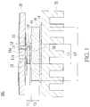
- Fig. 1 is a general sectional view of a heat dissipation structure 101 according to a first embodiment of the present invention.
- a heat spreader 31 as an example of a non-insulated thermal diffusion device (having a conductive heat dissipation part) is carried via a thin sheet-like insulated part 41 in a manner of bonding or contacting.
- a semiconductor device 10 as an example of a heating element and received in an ultrathin package 11 is carried, in a manner of bonding or contacting the heat dissipation surface 11b downwards, via the thin non-insulated part 32.
- the electrode 12 of the electric bonding surface 11a is electrically connected to a lower surface pattern 22 of the substrate 20 through welding or the like.
- the electrodes 12 and the heat dissipation electrode 13 are configured on an inner side relative to the appearance of the package 11, and are controlled to be a substantial package thickness T1.
- the package thickness T1 for example, is preferably below 2 mm.
- the thickness T2 of the heat spreader 31 is preferably, for example, above 2 mm, and the size thereof is greater than that of the semiconductor device 10 but less than that of the heat spreader 30. If the length of one side of the semiconductor device 10 is set as L1, the length L2 of each side of the heat spreader 31 is preferably set as above L1+2 ⁇ T2.
- a material thereof for example, high thermal conductivity metal whose thermal conductivity is above 190 W/mk may be listed, specifically, copper or aluminum may be listed, but it is not limited to the materials.
- the non-insulated part 32 for example, the material whose thermal conductivity is above 20 W/mk may be listed, specifically, solder or graphite may be listed, but it is not limited to the materials.
- the insulated part 41 for example, is set as a member whose thermal conductivity is 1 W/mk to 10 W/mk and withstanding voltage is above 1500 V, and in order to ensure an insulation distance, it is preferably greater than the heat spreader 31.
- the heat dissipation surface 11b of the semiconductor device 10 is contacted to the heat spreader 31 in a non-insulating manner, and the heat spreader 31 contacts the heat sink 30 in a non-insulating manner.
- heat produced by the semiconductor device 10 is transferred to the heat spreader 31 from the heat dissipation surface 11b via the non-insulated part 32 to be diffused, and then is transferred to the heat sink 30 via the insulated part 41, which thus has excellent heat dissipation.
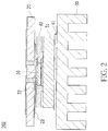
- Fig. 2 is a general sectional view of a heat dissipation structure 102 according to a second embodiment of the present invention.
- like reference signs are marked for components the same as those of the first embodiment, and the following focuses on describing their differences.
- a sectional horizontal L-shaped insulated part 42 is further inserted between the substrate 20 and the heat spreader 31 in a manner of covering the periphery of the semiconductor device 10 and the pattern of the substrate 20 (a pattern that at least can become a high voltage difference with the heat spreader 31).
- it is not limited to insertion of the insulated part 42, as long as it is configured through coating of the same insulating material or the like in a manner that the insulating material is present on the periphery of the semiconductor device 10. That is, it is set as a structure having an insulating layer of an insulating material in a space sandwiched between the substrate 20 and the heat spreader 31 on the periphery of the semiconductor device 10.
- an insulation heat-resistant resin e.g., PolyPhenylenesulfide (PPS)
- PPS PolyPhenylenesulfide
- an insulation heat-resistant resin e.g., epoxy or silicone or the like
- sealing element e.g., epoxy or silicone or the like
- a bonding or contacting portion of the heat spreader 31 to the package 11 of the semiconductor device 10 is higher than the surrounding.
- the heat dissipation structure 102 the heat dissipation surface 11b of the semiconductor device 10 is contacted to the heat spreader 31 in a non-insulating manner, and the heat spreader 31 contacts the heat sink 30 in an insulating manner, and then the periphery of the semiconductor device 10 and the pattern of the substrate 20 are covered by the insulated part 42.
- the structure can have excellent heat dissipation and can also avoid damage to insulation.
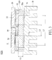
- Fig. 3 is a general sectional view of a heat dissipation structure 102A of a varying example of the second embodiment of the present invention.
- like reference signs are marked for components the same as those of the first embodiment, and the following focuses on describing their differences.
- an insulated part 42A that occupies the remaining space is inserted between the substrate 20 and the heat sink 30, and is fixed to a screw hole 30a disposed on the heat sink 30 by using a screw 50.
- the insulated part 42A, between the substrate 20 and the heat sink 30, not only covers the semiconductor device 10, but also covers the entire periphery also including a lower surface (also including a lower surface pattern 22) of the substrate 20, the non-insulated part 32, the heat spreader 31 and the insulated part 41.
- solder or graphite or the like may be listed, but it is not limited to the materials.
- the thickness T2 is preferably above 2 mm. If the length of one side of the semiconductor device 10 is set as L1, the size (the length of each side is set as L2) is preferably greater than L1+2 ⁇ T2 but less than the heat sink 30.
- an insulated sheet e.g., the thermal conductivity is 5 W/mk
- the thermal conductivity is 5 W/mk
- heat sink 30 for example, an aluminium-made heat sink may be listed, but it is not limited thereto.
- the heat dissipation structure 102A similar to the heat dissipation structure 102 of the second embodiment, the heat dissipation surface 11b of the semiconductor device 10 is contacted to the heat spreader 31 in a non-insulating manner, and the heat spreader 31 contacts the heat sink 30 in an insulating manner, and then the surrounding of the electrodes 12 of the semiconductor device 10 is covered by the insulated part 42A.
- the structure can have excellent heat dissipation and can also avoid damage to insulation.
Landscapes
- Cooling Or The Like Of Semiconductors Or Solid State Devices (AREA)
- Cooling Or The Like Of Electrical Apparatus (AREA)
- Physics & Mathematics (AREA)
- Geometry (AREA)
- Engineering & Computer Science (AREA)
- Microelectronics & Electronic Packaging (AREA)
Abstract
Description
- The present invention relates to a heat dissipation structure (also referred to as cooling structure) of a surface-mount semiconductor device, in particular, to a heat dissipation structure with heat dissipation and insulating reliability applicable to thin packaged semiconductor device.
-
Fig. 4(a) is a general stereogram of a lead typediscrete part 1 of the prior art, andFig. 4(b) is a general stereogram of a surface-mount semiconductor device 10 developed in recent years. - With high speed of a semiconductor switch element, parasitic inductance of the element has to be reduced. Different from the discrete part 1 (e.g., lead type Insulated Gate Bipolar Transistor (IGBT)) of the prior art shown in
Fig. 4(a) , for example, in thesemiconductor device 10 shown inFig. 4(b) , the speed of the switch is very high, and thus, in order to implement the parasitic inductance as small as possible, device package thinning is being promoted. - Such a
semiconductor device 10, as shown inFig. 4(b) , is received in anultrathin package 11, for example, it includes: anelectric bonding surface 11a provided with more than one electrode (terminal) 12 electrically connected with a substrate; and aheat dissipation surface 11b, wherein a largeheat dissipation electrode 13 is provided on an opposite side of theelectric bonding surface 11a. During mounting of thesemiconductor device 10, excellent heat dissipation and insulating reliability are required, for example, technologies ofPatent Document 1 to Patent Document 3 are proposed. -
- Patent Document 1: Japanese Patent Gazette No.
2014-241340 - Patent Document 2: Japanese Patent Gazette No.
2000-311971 - Patent Document 3: Japanese Patent Gazette No.
2008-028163 -
Fig. 5(a) is a general sectional view of aheat dissipation structure 201 of the prior art, andFig. 5(b) is a general sectional view of aheat dissipation structure 201A as the varying example. - In the
heat dissipation structure 201 shown inFig. 5(a) , on aheat sink 30 as an example of having a conductive heat-dissipation/cooling part (hereinafter referred to as "heat-dissipation part"), asemiconductor device 10 is carried via aninsulated part 41 in a manner of bonding or contacting theheat dissipation surface 11b downwards, and anelectrode 12 of theelectric bonding surface 11a is welded to alower surface pattern 22 of thesubstrate 20. - According to the
heat dissipation structure 201, heat produced by thesemiconductor device 10 is transferred to theheat sink 30 from theheat dissipation surface 11b via theinsulated part 41. - Moreover, in the
heat dissipation structure 201A shown inFig. 5(b) , thelower surface pattern 22 of thesubstrate 20 is contacted onto theheat sink 30 via theinsulated part 41, and anupper surface pattern 21 of thesubstrate 20 and theelectrode 12 of theelectric bonding surface 11a of thesemiconductor device 10 are welded together. - According to the
heat dissipation structure 201A, heat produced by thesemiconductor device 10 is transferred to theheat sink 30 from theelectrode 12 of theelectric bonding surface 11a via a thermal via or inlay disposed on thesubstrate 20 and theinsulated part 41. - The
heat dissipation structures semiconductor device 10 and theheat sink 30 as a heating element becomes minimum. Then, preferably, problem 2) to problem 4) can also be eliminated. - 1) heat dissipation (cooling) performance of the heating element (semiconductor device 10) (thermal conduction of the insulated part 41)
- 2) insulation of an upper surface electrode and a lower surface electrode on the
package 11 - 3) insulation of the
package 11 from the heat dissipation part - 4) electric wiring of the
substrate 20 and insulation of the heat dissipation part - In view of such problems of the former technology, the present invention is directed to a heat dissipation structure of a semiconductor device with excellent heat dissipation applicable to surface-mount thin semiconductor devices, and preferably, a heat dissipation structure of a semiconductor device also with excellent insulating reliability is provided.
- In order to achieve the objective, in the heat dissipation structure of the semiconductor device of the present invention, the semiconductor device has an electric bonding surface electrically connected with a substrate and a heat dissipation surface on an opposite side thereof, wherein the heat dissipation surface is bonded or contacted to a conductive member with high thermal conductivity via a non-insulated member, and the conductive member with high thermal conductivity is bonded or contacted to a heat dissipation part via a first insulated member.
- Herein, preferably, the thickness of the conductive member with high thermal conductivity is greater than that of the semiconductor device, the conductive member with high thermal conductivity, in a top view, is less than the heat dissipation part, and in a situation where the semiconductor device and the conductive member with high thermal conductivity, for example, are both set as a substantially rectangular shape in a top view, the length of each side of the conductive member with high thermal conductivity is greater than the sum of twice the thickness of the conductive member with high thermal conductivity and the length of each side of the semiconductor device. However, the conductive member with high thermal conductivity, in a top view, is not limited to the substantially rectangular shape, for example, it may also be a substantially round shape, as long as the size thereof is determined according to the substantially rectangular shape. Moreover, preferably, the first insulated member, in a top view, is greater than the conductive member with high thermal conductivity.
- According to the heat dissipation structure of a semiconductor device, heat produced by the semiconductor device is transferred to the conductive member with high thermal conductivity from the heat dissipation surface via the non-insulated member to be diffused, and then is transferred to the heat dissipation part via the first insulated member, which thus has excellent heat dissipation.
- In the heat dissipation structure of a semiconductor device of the present invention, it is also possible to configure a second insulated member between the substrate and the conductive member with high thermal conductivity in a manner of covering the periphery of the semiconductor device and at least one part of a pattern of the substrate. Then, the second insulated member may also be configured in a manner of occupying a space between the substrate and the heat dissipation part.
- Here, the second insulated member may also have a through-hole for fixing to the heat dissipation part. The second insulated member, for example, may also be configured through an insulation heat-resistant resin formed or cut processed product, an insulation heat-resistant tape, an insulation heat-resistant sealing element, or a combination of any two or more thereof.
- The heat dissipation structure of a semiconductor device with such a structure can have excellent heat dissipation and can also avoid damage to insulation.
- According to the heat dissipation structure of a semiconductor device of the present invention, heat produced by the semiconductor device is transferred to the conductive member with high thermal conductivity from the heat dissipation surface via the non-insulated member to be diffused, and then is transferred to the heat dissipation part via the first insulated member, which thus has excellent heat dissipation.
- Then, when a second insulated member is configured between the substrate and the conductive member with high thermal conductivity in a manner of covering the periphery of the semiconductor device and at least one part of a pattern of the substrate, the heat dissipation structure can have excellent heat dissipation and can also avoid damage to insulation.
-
-
Fig. 1 is a general sectional view of aheat dissipation structure 101 according to a first embodiment of the present invention. -
Fig. 2 is a general sectional view of aheat dissipation structure 102 according to a second embodiment of the present invention. -
Fig. 3 is a general sectional view of aheat dissipation structure 102A of a varying example of the second embodiment of the present invention. -
Fig. 4(a) is a general stereogram of a lead typediscrete part 1 of the prior art, andFig. 4(b) is a general stereogram of a surface-mount semiconductor device 10 like a GaN device developed in recent years. -
Fig. 5(a) is a general sectional view of aheat dissipation structure 201 of the prior art, andFig. 5(b) is a general sectional view of aheat dissipation structure 201A as a varying example thereof. - Several embodiments of the present invention are described below with reference to the accompanying drawings.
-
Fig. 1 is a general sectional view of aheat dissipation structure 101 according to a first embodiment of the present invention. - As shown in
Fig. 1 , in theheat dissipation structure 101, on a heat sink 30 (e.g., thermal conductivity is above 190 W/mk) as an example of having a conductive heat dissipation part, aheat spreader 31 as an example of a non-insulated thermal diffusion device (having a conductive heat dissipation part) is carried via a thin sheet-like insulatedpart 41 in a manner of bonding or contacting. On theheat spreader 31, asemiconductor device 10 as an example of a heating element and received in anultrathin package 11 is carried, in a manner of bonding or contacting theheat dissipation surface 11b downwards, via the thinnon-insulated part 32. Theelectrode 12 of theelectric bonding surface 11a is electrically connected to alower surface pattern 22 of thesubstrate 20 through welding or the like. - In the
semiconductor device 10, theelectrodes 12 and theheat dissipation electrode 13 are configured on an inner side relative to the appearance of thepackage 11, and are controlled to be a substantial package thickness T1. The package thickness T1, for example, is preferably below 2 mm. - The thickness T2 of the
heat spreader 31, is preferably, for example, above 2 mm, and the size thereof is greater than that of thesemiconductor device 10 but less than that of theheat spreader 30. If the length of one side of thesemiconductor device 10 is set as L1, the length L2 of each side of theheat spreader 31 is preferably set as above L1+2×T2. As a material thereof, for example, high thermal conductivity metal whose thermal conductivity is above 190 W/mk may be listed, specifically, copper or aluminum may be listed, but it is not limited to the materials. - As the
non-insulated part 32, for example, the material whose thermal conductivity is above 20 W/mk may be listed, specifically, solder or graphite may be listed, but it is not limited to the materials. - The
insulated part 41, for example, is set as a member whose thermal conductivity is 1 W/mk to 10 W/mk and withstanding voltage is above 1500 V, and in order to ensure an insulation distance, it is preferably greater than theheat spreader 31. - According to the
heat dissipation structure 101, theheat dissipation surface 11b of thesemiconductor device 10 is contacted to theheat spreader 31 in a non-insulating manner, and theheat spreader 31 contacts theheat sink 30 in a non-insulating manner. Thus, heat produced by thesemiconductor device 10 is transferred to theheat spreader 31 from theheat dissipation surface 11b via thenon-insulated part 32 to be diffused, and then is transferred to theheat sink 30 via theinsulated part 41, which thus has excellent heat dissipation. -
Fig. 2 is a general sectional view of aheat dissipation structure 102 according to a second embodiment of the present invention. In addition, like reference signs are marked for components the same as those of the first embodiment, and the following focuses on describing their differences. - As shown in
Fig. 2 , in theheat dissipation structure 102, in addition to the structure of theheat dissipation structure 101 of the first embodiment, a sectional horizontal L-shapedinsulated part 42 is further inserted between thesubstrate 20 and theheat spreader 31 in a manner of covering the periphery of thesemiconductor device 10 and the pattern of the substrate 20 (a pattern that at least can become a high voltage difference with the heat spreader 31). However, it is not limited to insertion of theinsulated part 42, as long as it is configured through coating of the same insulating material or the like in a manner that the insulating material is present on the periphery of thesemiconductor device 10. That is, it is set as a structure having an insulating layer of an insulating material in a space sandwiched between thesubstrate 20 and theheat spreader 31 on the periphery of thesemiconductor device 10. - As the
insulated part 42, for example, an insulation heat-resistant resin (e.g., PolyPhenylenesulfide (PPS)) formed or cut processed product, an insulation heat-resistant tape, an insulation heat-resistant resin (e.g., epoxy or silicone or the like) sealing element, or a combination of any two or more thereof may be listed, but it is not limited to the materials. - Preferably, a bonding or contacting portion of the
heat spreader 31 to thepackage 11 of thesemiconductor device 10 is higher than the surrounding. - According to the
heat dissipation structure 102, theheat dissipation surface 11b of thesemiconductor device 10 is contacted to theheat spreader 31 in a non-insulating manner, and theheat spreader 31 contacts theheat sink 30 in an insulating manner, and then the periphery of thesemiconductor device 10 and the pattern of thesubstrate 20 are covered by theinsulated part 42. Thus, the structure can have excellent heat dissipation and can also avoid damage to insulation. -
Fig. 3 is a general sectional view of aheat dissipation structure 102A of a varying example of the second embodiment of the present invention. In addition, like reference signs are marked for components the same as those of the first embodiment, and the following focuses on describing their differences. - As shown in
Fig. 3 , in theheat dissipation structure 102A, in place of theinsulated part 42 in the structure of theheat dissipation structure 102 of the second embodiment, aninsulated part 42A that occupies the remaining space is inserted between thesubstrate 20 and theheat sink 30, and is fixed to ascrew hole 30a disposed on theheat sink 30 by using ascrew 50. Theinsulated part 42A, between thesubstrate 20 and theheat sink 30, not only covers thesemiconductor device 10, but also covers the entire periphery also including a lower surface (also including a lower surface pattern 22) of thesubstrate 20, thenon-insulated part 32, theheat spreader 31 and theinsulated part 41. - As the
non-insulated part 32, solder or graphite or the like may be listed, but it is not limited to the materials. - As the
heat spreader 31, for example, copper-made heat spreaders may be listed, but it is not limited thereto. The thickness T2, for example, is preferably above 2 mm. If the length of one side of thesemiconductor device 10 is set as L1, the size (the length of each side is set as L2) is preferably greater than L1+2×T2 but less than theheat sink 30. - As the
insulated part 41, an insulated sheet (e.g., the thermal conductivity is 5 W/mk) may be listed, but it is not limited thereto. - As the
heat sink 30, for example, an aluminium-made heat sink may be listed, but it is not limited thereto. - According to the
heat dissipation structure 102A, similar to theheat dissipation structure 102 of the second embodiment, theheat dissipation surface 11b of thesemiconductor device 10 is contacted to theheat spreader 31 in a non-insulating manner, and theheat spreader 31 contacts theheat sink 30 in an insulating manner, and then the surrounding of theelectrodes 12 of thesemiconductor device 10 is covered by theinsulated part 42A. Thus, the structure can have excellent heat dissipation and can also avoid damage to insulation. - The structures of the embodiments described above and the varying examples thereof may also be combined with each other as long as there are no special obstructive factors or the like.
- In addition, the present invention can be implemented with other various forms without departing from its purport or main features. Therefore, the implementations or embodiments described are merely simple illustrations in all aspects, and should not be construed as limitations. The scope of the present invention is shown by the claims and is not subject to any constraint of the text of the specification. Then, variations or changes within the equivalent scope of the claims all fall within the scope of the present invention.
Claims (7)
- A heat dissipation structure of a semiconductor device, the semiconductor device(10) having an electric bonding surface(11a) electrically connected with a substrate(20) and a heat dissipation surface(11b) on an opposite side thereof, wherein
the heat dissipation surface(11b) is bonded or contacted to a conductive member with high thermal conductivity(31) via a non-insulated member(32), and
the conductive member with high thermal conductivity(31) is bonded or contacted to a heat dissipation part(30) via a first insulated member(41). - The heat dissipation structure of a semiconductor device according to claim 1, wherein
the thickness of the conductive member with high thermal conductivity(31) is greater than that of the semiconductor device(10),
the conductive member with high thermal conductivity(31), in a top view, is less than the heat dissipation part, and
in a situation where the semiconductor device(10) and the conductive member with high thermal conductivity(31) are both set as a substantially rectangular shape in a top view, length of each side of the conductive member with high thermal conductivity(31) is greater than the sum of twice the thickness of the conductive member with high thermal conductivity(31) and length of each side of the semiconductor device(10). - The heat dissipation structure of a semiconductor device according to claim 1 or 2, wherein
the first insulated member(41), in a top view, is greater than the conductive member with high thermal conductivity(31). - The heat dissipation structure of a semiconductor device according to any of claims 1 to 3, wherein
a second insulated member(42) is configured between the substrate(20) and the conductive member with high thermal conductivity(31) in a manner of covering the periphery of the semiconductor device(10) and at least one part of a pattern of the substrate(20). - The heat dissipation structure of a semiconductor device according to claim 4, wherein
the second insulated member(42) is configured in a manner of occupying a space between the substrate(20) and the heat dissipation part(30). - The heat dissipation structure of a semiconductor device according to claim 5, wherein
the second insulated member has a through-hole for fixing to the heat dissipation part. - The heat dissipation structure of a semiconductor device according to any of claims 4 to 6, wherein
the second insulated member(42) is configured through an insulation heat-resistant resin formed or cut processed product, an insulation heat-resistant tape, an insulation heat-resistant sealing element, or a combination of any two or more thereof.
Applications Claiming Priority (1)
| Application Number | Priority Date | Filing Date | Title |
|---|---|---|---|
| JP2016081964A JP6711098B2 (en) | 2016-04-15 | 2016-04-15 | Heat dissipation structure of semiconductor device |
Publications (2)
| Publication Number | Publication Date |
|---|---|
| EP3232468A1 true EP3232468A1 (en) | 2017-10-18 |
| EP3232468B1 EP3232468B1 (en) | 2021-01-06 |
Family
ID=57838279
Family Applications (1)
| Application Number | Title | Priority Date | Filing Date |
|---|---|---|---|
| EP17151972.1A Not-in-force EP3232468B1 (en) | 2016-04-15 | 2017-01-18 | Heat dissipation structure of a semiconductor device |
Country Status (7)
| Country | Link |
|---|---|
| US (1) | US9997430B2 (en) |
| EP (1) | EP3232468B1 (en) |
| JP (1) | JP6711098B2 (en) |
| KR (1) | KR101946467B1 (en) |
| CN (1) | CN107301987B (en) |
| PT (1) | PT3232468T (en) |
| TW (1) | TWI648829B (en) |
Cited By (1)
| Publication number | Priority date | Publication date | Assignee | Title |
|---|---|---|---|---|
| EP4297080A1 (en) * | 2022-06-20 | 2023-12-27 | Siemens Aktiengesellschaft | Circuit assembly with a circuit carrier and a semiconductor module |
Families Citing this family (5)
| Publication number | Priority date | Publication date | Assignee | Title |
|---|---|---|---|---|
| JP6693441B2 (en) * | 2017-02-27 | 2020-05-13 | オムロン株式会社 | Electronic device and manufacturing method thereof |
| CN110137720B (en) * | 2018-02-09 | 2022-07-26 | 富士康(昆山)电脑接插件有限公司 | Fixing device for fixing radiator and abutting device thereof |
| KR102185824B1 (en) | 2019-01-04 | 2020-12-02 | 강병혁 | Heat dissipation structure of semiconductor package for power conversion |
| JP7675595B2 (en) * | 2021-08-18 | 2025-05-13 | 三菱電機株式会社 | Semiconductor Module |
| JP7771709B2 (en) | 2021-12-14 | 2025-11-18 | オムロン株式会社 | Mounting boards and electrical devices equipped with mounting boards |
Citations (11)
| Publication number | Priority date | Publication date | Assignee | Title |
|---|---|---|---|---|
| US6111322A (en) * | 1996-05-20 | 2000-08-29 | Hitachi, Ltd. | Semiconductor device and manufacturing method thereof |
| JP2000311971A (en) | 1999-04-28 | 2000-11-07 | Hitachi Ltd | Semiconductor device and its heat sink |
| JP2008028163A (en) | 2006-07-21 | 2008-02-07 | Mitsubishi Materials Corp | Power module device |
| DE60315469T2 (en) * | 2003-10-29 | 2008-04-24 | Power One Italy S.P.A. | Heat dissipating insert, circuit with such an insert and method of manufacture |
| US20100327431A1 (en) * | 2009-06-29 | 2010-12-30 | Touzelbaev Maxat N | Semiconductor Chip Thermal Interface Structures |
| US20110240279A1 (en) * | 2010-03-30 | 2011-10-06 | International Business Machines Corporation | Hybrid liquid metal-solder thermal interface |
| US20130314877A1 (en) * | 2012-05-28 | 2013-11-28 | Fujitsu Limited | Semiconductor package and wiring board unit |
| EP2770530A2 (en) * | 2013-02-22 | 2014-08-27 | Fujitsu Limited | Electronic component unit and fixing structure |
| US20140239482A1 (en) * | 2013-02-26 | 2014-08-28 | Shinobu Kourakata | Integrated heat spreader for multi-chip packages |
| JP2014241340A (en) | 2013-06-11 | 2014-12-25 | 株式会社デンソー | Heat radiation insulation sheet and semiconductor apparatus |
| DE102014205958A1 (en) * | 2014-03-31 | 2015-10-01 | Lemförder Electronic GmbH | Semiconductor switching element arrangement and control device for a vehicle |
Family Cites Families (25)
| Publication number | Priority date | Publication date | Assignee | Title |
|---|---|---|---|---|
| JPH0458551A (en) * | 1990-06-28 | 1992-02-25 | Nec Corp | Multichip module |
| JPH08264688A (en) * | 1995-03-28 | 1996-10-11 | Sumitomo Kinzoku Electro Device:Kk | Ceramic package for semiconductor |
| JPH09139451A (en) * | 1995-11-15 | 1997-05-27 | Hitachi Ltd | Semiconductor device with heat radiation fin, mounting method and removal method thereof |
| JPH09213847A (en) * | 1996-02-01 | 1997-08-15 | Hitachi Ltd | Semiconductor integrated circuit device, manufacturing method thereof, and electronic device using the same |
| US6292367B1 (en) * | 2000-06-22 | 2001-09-18 | International Business Machines Corporation | Thermally efficient semiconductor chip |
| JP3855726B2 (en) | 2001-10-23 | 2006-12-13 | 松下電器産業株式会社 | Power module |
| JP3934565B2 (en) * | 2003-02-21 | 2007-06-20 | 富士通株式会社 | Semiconductor device |
| JP4173751B2 (en) * | 2003-02-28 | 2008-10-29 | 株式会社ルネサステクノロジ | Semiconductor device |
| TWI242863B (en) * | 2003-09-15 | 2005-11-01 | Siliconware Precision Industries Co Ltd | Heat dissipating structure and semiconductor package with the heat dissipating structure |
| US20050133908A1 (en) * | 2003-12-18 | 2005-06-23 | Advanced Thermal Technologies | Chip assembly with glue-strengthening holes |
| JP4986435B2 (en) * | 2005-10-12 | 2012-07-25 | 株式会社ソニー・コンピュータエンタテインメント | Semiconductor device and method for producing semiconductor device |
| TW200824073A (en) * | 2006-11-24 | 2008-06-01 | Siliconware Precision Industries Co Ltd | Heat-dissipation semiconductor package and fabrication method thereof |
| TWI355048B (en) * | 2006-12-13 | 2011-12-21 | Siliconware Precision Industries Co Ltd | Heat-dissipation semiconductor package and heat-di |
| TWI353047B (en) * | 2006-12-28 | 2011-11-21 | Siliconware Precision Industries Co Ltd | Heat-dissipating-type semiconductor package |
| JP4539773B2 (en) * | 2008-03-07 | 2010-09-08 | 株式会社デンソー | Semiconductor device and manufacturing method thereof |
| CN101960591A (en) * | 2008-03-28 | 2011-01-26 | 日本电气株式会社 | Semiconductor device, semiconductor device manufacturing method, printed circuit board and electronic device |
| CN102714195B (en) * | 2009-12-14 | 2015-05-06 | 松下电器产业株式会社 | Semiconductor device |
| JP2012033559A (en) * | 2010-07-28 | 2012-02-16 | J Devices:Kk | Semiconductor device |
| JP2012074425A (en) * | 2010-09-28 | 2012-04-12 | Daikin Ind Ltd | Power module |
| KR101198848B1 (en) * | 2010-12-22 | 2012-11-07 | (주)포인트엔지니어링 | Semiconductor Device and Fabricating Method thereof |
| JP2013004953A (en) * | 2011-06-22 | 2013-01-07 | Denso Corp | Electronic control device |
| WO2013051387A1 (en) * | 2011-10-07 | 2013-04-11 | 富士電機株式会社 | Pcb attachment structure and semiconductor device using structure |
| US8952503B2 (en) * | 2013-01-29 | 2015-02-10 | International Business Machines Corporation | Organic module EMI shielding structures and methods |
| US9576930B2 (en) * | 2013-11-08 | 2017-02-21 | Taiwan Semiconductor Manufacturing Co., Ltd. | Thermally conductive structure for heat dissipation in semiconductor packages |
| WO2015072428A1 (en) * | 2013-11-12 | 2015-05-21 | Jnc株式会社 | Heat sink |
-
2016
- 2016-04-15 JP JP2016081964A patent/JP6711098B2/en not_active Expired - Fee Related
-
2017
- 2017-01-18 PT PT171519721T patent/PT3232468T/en unknown
- 2017-01-18 EP EP17151972.1A patent/EP3232468B1/en not_active Not-in-force
- 2017-01-20 CN CN201710045272.7A patent/CN107301987B/en not_active Expired - Fee Related
- 2017-01-20 US US15/410,781 patent/US9997430B2/en not_active Expired - Fee Related
- 2017-03-23 TW TW106109642A patent/TWI648829B/en not_active IP Right Cessation
- 2017-03-29 KR KR1020170039895A patent/KR101946467B1/en not_active Expired - Fee Related
Patent Citations (11)
| Publication number | Priority date | Publication date | Assignee | Title |
|---|---|---|---|---|
| US6111322A (en) * | 1996-05-20 | 2000-08-29 | Hitachi, Ltd. | Semiconductor device and manufacturing method thereof |
| JP2000311971A (en) | 1999-04-28 | 2000-11-07 | Hitachi Ltd | Semiconductor device and its heat sink |
| DE60315469T2 (en) * | 2003-10-29 | 2008-04-24 | Power One Italy S.P.A. | Heat dissipating insert, circuit with such an insert and method of manufacture |
| JP2008028163A (en) | 2006-07-21 | 2008-02-07 | Mitsubishi Materials Corp | Power module device |
| US20100327431A1 (en) * | 2009-06-29 | 2010-12-30 | Touzelbaev Maxat N | Semiconductor Chip Thermal Interface Structures |
| US20110240279A1 (en) * | 2010-03-30 | 2011-10-06 | International Business Machines Corporation | Hybrid liquid metal-solder thermal interface |
| US20130314877A1 (en) * | 2012-05-28 | 2013-11-28 | Fujitsu Limited | Semiconductor package and wiring board unit |
| EP2770530A2 (en) * | 2013-02-22 | 2014-08-27 | Fujitsu Limited | Electronic component unit and fixing structure |
| US20140239482A1 (en) * | 2013-02-26 | 2014-08-28 | Shinobu Kourakata | Integrated heat spreader for multi-chip packages |
| JP2014241340A (en) | 2013-06-11 | 2014-12-25 | 株式会社デンソー | Heat radiation insulation sheet and semiconductor apparatus |
| DE102014205958A1 (en) * | 2014-03-31 | 2015-10-01 | Lemförder Electronic GmbH | Semiconductor switching element arrangement and control device for a vehicle |
Cited By (2)
| Publication number | Priority date | Publication date | Assignee | Title |
|---|---|---|---|---|
| EP4297080A1 (en) * | 2022-06-20 | 2023-12-27 | Siemens Aktiengesellschaft | Circuit assembly with a circuit carrier and a semiconductor module |
| WO2023247103A1 (en) * | 2022-06-20 | 2023-12-28 | Siemens Aktiengesellschaft | Circuit assembly with a circuit carrier and a semiconductor component |
Also Published As
| Publication number | Publication date |
|---|---|
| TW201803049A (en) | 2018-01-16 |
| KR101946467B1 (en) | 2019-02-08 |
| KR20170118599A (en) | 2017-10-25 |
| US9997430B2 (en) | 2018-06-12 |
| CN107301987A (en) | 2017-10-27 |
| US20170301602A1 (en) | 2017-10-19 |
| PT3232468T (en) | 2021-01-18 |
| JP2017191904A (en) | 2017-10-19 |
| CN107301987B (en) | 2019-11-05 |
| JP6711098B2 (en) | 2020-06-17 |
| EP3232468B1 (en) | 2021-01-06 |
| TWI648829B (en) | 2019-01-21 |
Similar Documents
| Publication | Publication Date | Title |
|---|---|---|
| US9997430B2 (en) | Heat dissipation structure of semiconductor device | |
| US9728484B2 (en) | Power module package and method for manufacturing the same | |
| US10170394B2 (en) | Semiconductor device | |
| US20150214138A1 (en) | Semiconductor device | |
| US10672677B2 (en) | Semiconductor package structure | |
| US9433075B2 (en) | Electric power semiconductor device | |
| US10468315B2 (en) | Power module | |
| US9666557B2 (en) | Small footprint semiconductor package | |
| KR102499825B1 (en) | Packaged power semiconductor device | |
| US11315850B2 (en) | Semiconductor device | |
| US10510636B2 (en) | Electronic module | |
| US11081412B2 (en) | Semiconductor device | |
| JP6834815B2 (en) | Semiconductor module | |
| US10600712B2 (en) | Electronic device | |
| CN107851631B (en) | semiconductor device | |
| CN104934398B (en) | Electronic unit and lead frame | |
| US20170194296A1 (en) | Semiconductor module | |
| CN107026129A (en) | Semiconductor device | |
| EP3327768A1 (en) | Heat dissipation structure of semiconductor device | |
| US9099451B2 (en) | Power module package and method of manufacturing the same | |
| JP2017005129A (en) | Semiconductor device | |
| CN109671687A (en) | Power module | |
| US20150179540A1 (en) | Semiconductor device | |
| US11257732B2 (en) | Semiconductor module and semiconductor device | |
| KR20160093267A (en) | Power semiconductor module |
Legal Events
| Date | Code | Title | Description |
|---|---|---|---|
| PUAI | Public reference made under article 153(3) epc to a published international application that has entered the european phase |
Free format text: ORIGINAL CODE: 0009012 |
|
| STAA | Information on the status of an ep patent application or granted ep patent |
Free format text: STATUS: REQUEST FOR EXAMINATION WAS MADE |
|
| 17P | Request for examination filed |
Effective date: 20170118 |
|
| AK | Designated contracting states |
Kind code of ref document: A1 Designated state(s): AL AT BE BG CH CY CZ DE DK EE ES FI FR GB GR HR HU IE IS IT LI LT LU LV MC MK MT NL NO PL PT RO RS SE SI SK SM TR |
|
| AX | Request for extension of the european patent |
Extension state: BA ME |
|
| RBV | Designated contracting states (corrected) |
Designated state(s): AL AT BE BG CH CY CZ DE DK EE ES FI FR GB GR HR HU IE IS IT LI LT LU LV MC MK MT NL NO PL PT RO RS SE SI SK SM TR |
|
| GRAJ | Information related to disapproval of communication of intention to grant by the applicant or resumption of examination proceedings by the epo deleted |
Free format text: ORIGINAL CODE: EPIDOSDIGR1 |
|
| STAA | Information on the status of an ep patent application or granted ep patent |
Free format text: STATUS: GRANT OF PATENT IS INTENDED |
|
| GRAP | Despatch of communication of intention to grant a patent |
Free format text: ORIGINAL CODE: EPIDOSNIGR1 |
|
| INTG | Intention to grant announced |
Effective date: 20200803 |
|
| GRAS | Grant fee paid |
Free format text: ORIGINAL CODE: EPIDOSNIGR3 |
|
| GRAA | (expected) grant |
Free format text: ORIGINAL CODE: 0009210 |
|
| STAA | Information on the status of an ep patent application or granted ep patent |
Free format text: STATUS: THE PATENT HAS BEEN GRANTED |
|
| AK | Designated contracting states |
Kind code of ref document: B1 Designated state(s): AL AT BE BG CH CY CZ DE DK EE ES FI FR GB GR HR HU IE IS IT LI LT LU LV MC MK MT NL NO PL PT RO RS SE SI SK SM TR |
|
| REG | Reference to a national code |
Ref country code: GB Ref legal event code: FG4D |
|
| REG | Reference to a national code |
Ref country code: AT Ref legal event code: REF Ref document number: 1353288 Country of ref document: AT Kind code of ref document: T Effective date: 20210115 Ref country code: CH Ref legal event code: EP |
|
| REG | Reference to a national code |
Ref country code: PT Ref legal event code: SC4A Ref document number: 3232468 Country of ref document: PT Date of ref document: 20210118 Kind code of ref document: T Free format text: AVAILABILITY OF NATIONAL TRANSLATION Effective date: 20210112 |
|
| REG | Reference to a national code |
Ref country code: DE Ref legal event code: R096 Ref document number: 602017030750 Country of ref document: DE |
|
| REG | Reference to a national code |
Ref country code: IE Ref legal event code: FG4D |
|
| REG | Reference to a national code |
Ref country code: NL Ref legal event code: FP |
|
| PGFP | Annual fee paid to national office [announced via postgrant information from national office to epo] |
Ref country code: IT Payment date: 20210329 Year of fee payment: 5 Ref country code: FR Payment date: 20210128 Year of fee payment: 5 Ref country code: NL Payment date: 20210113 Year of fee payment: 5 Ref country code: PT Payment date: 20210113 Year of fee payment: 5 |
|
| PGFP | Annual fee paid to national office [announced via postgrant information from national office to epo] |
Ref country code: DE Payment date: 20201224 Year of fee payment: 5 |
|
| REG | Reference to a national code |
Ref country code: AT Ref legal event code: MK05 Ref document number: 1353288 Country of ref document: AT Kind code of ref document: T Effective date: 20210106 |
|
| REG | Reference to a national code |
Ref country code: LT Ref legal event code: MG9D |
|
| PG25 | Lapsed in a contracting state [announced via postgrant information from national office to epo] |
Ref country code: HR Free format text: LAPSE BECAUSE OF FAILURE TO SUBMIT A TRANSLATION OF THE DESCRIPTION OR TO PAY THE FEE WITHIN THE PRESCRIBED TIME-LIMIT Effective date: 20210106 Ref country code: GR Free format text: LAPSE BECAUSE OF FAILURE TO SUBMIT A TRANSLATION OF THE DESCRIPTION OR TO PAY THE FEE WITHIN THE PRESCRIBED TIME-LIMIT Effective date: 20210407 Ref country code: FI Free format text: LAPSE BECAUSE OF FAILURE TO SUBMIT A TRANSLATION OF THE DESCRIPTION OR TO PAY THE FEE WITHIN THE PRESCRIBED TIME-LIMIT Effective date: 20210106 Ref country code: NO Free format text: LAPSE BECAUSE OF FAILURE TO SUBMIT A TRANSLATION OF THE DESCRIPTION OR TO PAY THE FEE WITHIN THE PRESCRIBED TIME-LIMIT Effective date: 20210406 Ref country code: LT Free format text: LAPSE BECAUSE OF FAILURE TO SUBMIT A TRANSLATION OF THE DESCRIPTION OR TO PAY THE FEE WITHIN THE PRESCRIBED TIME-LIMIT Effective date: 20210106 Ref country code: BG Free format text: LAPSE BECAUSE OF FAILURE TO SUBMIT A TRANSLATION OF THE DESCRIPTION OR TO PAY THE FEE WITHIN THE PRESCRIBED TIME-LIMIT Effective date: 20210406 |
|
| PG25 | Lapsed in a contracting state [announced via postgrant information from national office to epo] |
Ref country code: SE Free format text: LAPSE BECAUSE OF FAILURE TO SUBMIT A TRANSLATION OF THE DESCRIPTION OR TO PAY THE FEE WITHIN THE PRESCRIBED TIME-LIMIT Effective date: 20210106 Ref country code: AT Free format text: LAPSE BECAUSE OF FAILURE TO SUBMIT A TRANSLATION OF THE DESCRIPTION OR TO PAY THE FEE WITHIN THE PRESCRIBED TIME-LIMIT Effective date: 20210106 Ref country code: RS Free format text: LAPSE BECAUSE OF FAILURE TO SUBMIT A TRANSLATION OF THE DESCRIPTION OR TO PAY THE FEE WITHIN THE PRESCRIBED TIME-LIMIT Effective date: 20210106 Ref country code: PL Free format text: LAPSE BECAUSE OF FAILURE TO SUBMIT A TRANSLATION OF THE DESCRIPTION OR TO PAY THE FEE WITHIN THE PRESCRIBED TIME-LIMIT Effective date: 20210106 Ref country code: LV Free format text: LAPSE BECAUSE OF FAILURE TO SUBMIT A TRANSLATION OF THE DESCRIPTION OR TO PAY THE FEE WITHIN THE PRESCRIBED TIME-LIMIT Effective date: 20210106 |
|
| PGFP | Annual fee paid to national office [announced via postgrant information from national office to epo] |
Ref country code: GB Payment date: 20210423 Year of fee payment: 5 |
|
| REG | Reference to a national code |
Ref country code: CH Ref legal event code: PL |
|
| PG25 | Lapsed in a contracting state [announced via postgrant information from national office to epo] |
Ref country code: LU Free format text: LAPSE BECAUSE OF NON-PAYMENT OF DUE FEES Effective date: 20210118 Ref country code: IS Free format text: LAPSE BECAUSE OF FAILURE TO SUBMIT A TRANSLATION OF THE DESCRIPTION OR TO PAY THE FEE WITHIN THE PRESCRIBED TIME-LIMIT Effective date: 20210506 |
|
| REG | Reference to a national code |
Ref country code: BE Ref legal event code: MM Effective date: 20210131 |
|
| REG | Reference to a national code |
Ref country code: DE Ref legal event code: R097 Ref document number: 602017030750 Country of ref document: DE |
|
| PG25 | Lapsed in a contracting state [announced via postgrant information from national office to epo] |
Ref country code: SM Free format text: LAPSE BECAUSE OF FAILURE TO SUBMIT A TRANSLATION OF THE DESCRIPTION OR TO PAY THE FEE WITHIN THE PRESCRIBED TIME-LIMIT Effective date: 20210106 Ref country code: EE Free format text: LAPSE BECAUSE OF FAILURE TO SUBMIT A TRANSLATION OF THE DESCRIPTION OR TO PAY THE FEE WITHIN THE PRESCRIBED TIME-LIMIT Effective date: 20210106 Ref country code: CZ Free format text: LAPSE BECAUSE OF FAILURE TO SUBMIT A TRANSLATION OF THE DESCRIPTION OR TO PAY THE FEE WITHIN THE PRESCRIBED TIME-LIMIT Effective date: 20210106 Ref country code: MC Free format text: LAPSE BECAUSE OF FAILURE TO SUBMIT A TRANSLATION OF THE DESCRIPTION OR TO PAY THE FEE WITHIN THE PRESCRIBED TIME-LIMIT Effective date: 20210106 |
|
| PLBE | No opposition filed within time limit |
Free format text: ORIGINAL CODE: 0009261 |
|
| STAA | Information on the status of an ep patent application or granted ep patent |
Free format text: STATUS: NO OPPOSITION FILED WITHIN TIME LIMIT |
|
| PG25 | Lapsed in a contracting state [announced via postgrant information from national office to epo] |
Ref country code: SK Free format text: LAPSE BECAUSE OF FAILURE TO SUBMIT A TRANSLATION OF THE DESCRIPTION OR TO PAY THE FEE WITHIN THE PRESCRIBED TIME-LIMIT Effective date: 20210106 Ref country code: RO Free format text: LAPSE BECAUSE OF FAILURE TO SUBMIT A TRANSLATION OF THE DESCRIPTION OR TO PAY THE FEE WITHIN THE PRESCRIBED TIME-LIMIT Effective date: 20210106 Ref country code: CH Free format text: LAPSE BECAUSE OF NON-PAYMENT OF DUE FEES Effective date: 20210131 Ref country code: DK Free format text: LAPSE BECAUSE OF FAILURE TO SUBMIT A TRANSLATION OF THE DESCRIPTION OR TO PAY THE FEE WITHIN THE PRESCRIBED TIME-LIMIT Effective date: 20210106 Ref country code: LI Free format text: LAPSE BECAUSE OF NON-PAYMENT OF DUE FEES Effective date: 20210131 |
|
| 26N | No opposition filed |
Effective date: 20211007 |
|
| PG25 | Lapsed in a contracting state [announced via postgrant information from national office to epo] |
Ref country code: AL Free format text: LAPSE BECAUSE OF FAILURE TO SUBMIT A TRANSLATION OF THE DESCRIPTION OR TO PAY THE FEE WITHIN THE PRESCRIBED TIME-LIMIT Effective date: 20210106 Ref country code: IE Free format text: LAPSE BECAUSE OF NON-PAYMENT OF DUE FEES Effective date: 20210118 Ref country code: ES Free format text: LAPSE BECAUSE OF FAILURE TO SUBMIT A TRANSLATION OF THE DESCRIPTION OR TO PAY THE FEE WITHIN THE PRESCRIBED TIME-LIMIT Effective date: 20210106 |
|
| PG25 | Lapsed in a contracting state [announced via postgrant information from national office to epo] |
Ref country code: SI Free format text: LAPSE BECAUSE OF FAILURE TO SUBMIT A TRANSLATION OF THE DESCRIPTION OR TO PAY THE FEE WITHIN THE PRESCRIBED TIME-LIMIT Effective date: 20210106 |
|
| PG25 | Lapsed in a contracting state [announced via postgrant information from national office to epo] |
Ref country code: IS Free format text: LAPSE BECAUSE OF FAILURE TO SUBMIT A TRANSLATION OF THE DESCRIPTION OR TO PAY THE FEE WITHIN THE PRESCRIBED TIME-LIMIT Effective date: 20210506 |
|
| PG25 | Lapsed in a contracting state [announced via postgrant information from national office to epo] |
Ref country code: BE Free format text: LAPSE BECAUSE OF NON-PAYMENT OF DUE FEES Effective date: 20210131 |
|
| REG | Reference to a national code |
Ref country code: DE Ref legal event code: R119 Ref document number: 602017030750 Country of ref document: DE |
|
| REG | Reference to a national code |
Ref country code: NL Ref legal event code: MM Effective date: 20220201 |
|
| GBPC | Gb: european patent ceased through non-payment of renewal fee |
Effective date: 20220118 |
|
| PG25 | Lapsed in a contracting state [announced via postgrant information from national office to epo] |
Ref country code: PT Free format text: LAPSE BECAUSE OF NON-PAYMENT OF DUE FEES Effective date: 20220718 Ref country code: NL Free format text: LAPSE BECAUSE OF NON-PAYMENT OF DUE FEES Effective date: 20220201 Ref country code: GB Free format text: LAPSE BECAUSE OF NON-PAYMENT OF DUE FEES Effective date: 20220118 Ref country code: DE Free format text: LAPSE BECAUSE OF NON-PAYMENT OF DUE FEES Effective date: 20220802 |
|
| PG25 | Lapsed in a contracting state [announced via postgrant information from national office to epo] |
Ref country code: FR Free format text: LAPSE BECAUSE OF NON-PAYMENT OF DUE FEES Effective date: 20220131 |
|
| PG25 | Lapsed in a contracting state [announced via postgrant information from national office to epo] |
Ref country code: IT Free format text: LAPSE BECAUSE OF NON-PAYMENT OF DUE FEES Effective date: 20220118 |
|
| PG25 | Lapsed in a contracting state [announced via postgrant information from national office to epo] |
Ref country code: HU Free format text: LAPSE BECAUSE OF FAILURE TO SUBMIT A TRANSLATION OF THE DESCRIPTION OR TO PAY THE FEE WITHIN THE PRESCRIBED TIME-LIMIT; INVALID AB INITIO Effective date: 20170118 |
|
| PG25 | Lapsed in a contracting state [announced via postgrant information from national office to epo] |
Ref country code: CY Free format text: LAPSE BECAUSE OF FAILURE TO SUBMIT A TRANSLATION OF THE DESCRIPTION OR TO PAY THE FEE WITHIN THE PRESCRIBED TIME-LIMIT Effective date: 20210106 |
|
| PG25 | Lapsed in a contracting state [announced via postgrant information from national office to epo] |
Ref country code: MK Free format text: LAPSE BECAUSE OF FAILURE TO SUBMIT A TRANSLATION OF THE DESCRIPTION OR TO PAY THE FEE WITHIN THE PRESCRIBED TIME-LIMIT Effective date: 20210106 |
|
| PG25 | Lapsed in a contracting state [announced via postgrant information from national office to epo] |
Ref country code: TR Free format text: LAPSE BECAUSE OF FAILURE TO SUBMIT A TRANSLATION OF THE DESCRIPTION OR TO PAY THE FEE WITHIN THE PRESCRIBED TIME-LIMIT Effective date: 20210106 |
|
| PG25 | Lapsed in a contracting state [announced via postgrant information from national office to epo] |
Ref country code: MT Free format text: LAPSE BECAUSE OF FAILURE TO SUBMIT A TRANSLATION OF THE DESCRIPTION OR TO PAY THE FEE WITHIN THE PRESCRIBED TIME-LIMIT Effective date: 20210106 |