EP3229560B1 - Flächenelement zum leuchten und heizen - Google Patents
Flächenelement zum leuchten und heizen Download PDFInfo
- Publication number
- EP3229560B1 EP3229560B1 EP17000667.0A EP17000667A EP3229560B1 EP 3229560 B1 EP3229560 B1 EP 3229560B1 EP 17000667 A EP17000667 A EP 17000667A EP 3229560 B1 EP3229560 B1 EP 3229560B1
- Authority
- EP
- European Patent Office
- Prior art keywords
- layer
- illumination
- heating
- planar element
- element according
- Prior art date
- Legal status (The legal status is an assumption and is not a legal conclusion. Google has not performed a legal analysis and makes no representation as to the accuracy of the status listed.)
- Active
Links
Images


Classifications
-
- H—ELECTRICITY
- H05—ELECTRIC TECHNIQUES NOT OTHERWISE PROVIDED FOR
- H05B—ELECTRIC HEATING; ELECTRIC LIGHT SOURCES NOT OTHERWISE PROVIDED FOR; CIRCUIT ARRANGEMENTS FOR ELECTRIC LIGHT SOURCES, IN GENERAL
- H05B33/00—Electroluminescent light sources
- H05B33/12—Light sources with substantially two-dimensional [2D] radiating surfaces
-
- G—PHYSICS
- G09—EDUCATION; CRYPTOGRAPHY; DISPLAY; ADVERTISING; SEALS
- G09F—DISPLAYING; ADVERTISING; SIGNS; LABELS OR NAME-PLATES; SEALS
- G09F13/00—Illuminated signs; Luminous advertising
- G09F13/20—Illuminated signs; Luminous advertising with luminescent surfaces or parts
- G09F13/22—Illuminated signs; Luminous advertising with luminescent surfaces or parts electroluminescent
-
- H—ELECTRICITY
- H10—SEMICONDUCTOR DEVICES; ELECTRIC SOLID-STATE DEVICES NOT OTHERWISE PROVIDED FOR
- H10K—ORGANIC ELECTRIC SOLID-STATE DEVICES
- H10K30/00—Organic devices sensitive to infrared radiation, light, electromagnetic radiation of shorter wavelength or corpuscular radiation
- H10K30/80—Constructional details
- H10K30/88—Passivation; Containers; Encapsulations
-
- H—ELECTRICITY
- H10—SEMICONDUCTOR DEVICES; ELECTRIC SOLID-STATE DEVICES NOT OTHERWISE PROVIDED FOR
- H10K—ORGANIC ELECTRIC SOLID-STATE DEVICES
- H10K71/00—Manufacture or treatment specially adapted for the organic devices covered by this subclass
- H10K71/10—Deposition of organic active material
- H10K71/12—Deposition of organic active material using liquid deposition, e.g. spin coating
- H10K71/13—Deposition of organic active material using liquid deposition, e.g. spin coating using printing techniques, e.g. ink-jet printing or screen printing
-
- H—ELECTRICITY
- H10—SEMICONDUCTOR DEVICES; ELECTRIC SOLID-STATE DEVICES NOT OTHERWISE PROVIDED FOR
- H10K—ORGANIC ELECTRIC SOLID-STATE DEVICES
- H10K30/00—Organic devices sensitive to infrared radiation, light, electromagnetic radiation of shorter wavelength or corpuscular radiation
-
- H—ELECTRICITY
- H10—SEMICONDUCTOR DEVICES; ELECTRIC SOLID-STATE DEVICES NOT OTHERWISE PROVIDED FOR
- H10K—ORGANIC ELECTRIC SOLID-STATE DEVICES
- H10K30/00—Organic devices sensitive to infrared radiation, light, electromagnetic radiation of shorter wavelength or corpuscular radiation
- H10K30/50—Photovoltaic [PV] devices
-
- Y—GENERAL TAGGING OF NEW TECHNOLOGICAL DEVELOPMENTS; GENERAL TAGGING OF CROSS-SECTIONAL TECHNOLOGIES SPANNING OVER SEVERAL SECTIONS OF THE IPC; TECHNICAL SUBJECTS COVERED BY FORMER USPC CROSS-REFERENCE ART COLLECTIONS [XRACs] AND DIGESTS
- Y02—TECHNOLOGIES OR APPLICATIONS FOR MITIGATION OR ADAPTATION AGAINST CLIMATE CHANGE
- Y02E—REDUCTION OF GREENHOUSE GAS [GHG] EMISSIONS, RELATED TO ENERGY GENERATION, TRANSMISSION OR DISTRIBUTION
- Y02E10/00—Energy generation through renewable energy sources
- Y02E10/50—Photovoltaic [PV] energy
- Y02E10/549—Organic PV cells
-
- Y—GENERAL TAGGING OF NEW TECHNOLOGICAL DEVELOPMENTS; GENERAL TAGGING OF CROSS-SECTIONAL TECHNOLOGIES SPANNING OVER SEVERAL SECTIONS OF THE IPC; TECHNICAL SUBJECTS COVERED BY FORMER USPC CROSS-REFERENCE ART COLLECTIONS [XRACs] AND DIGESTS
- Y02—TECHNOLOGIES OR APPLICATIONS FOR MITIGATION OR ADAPTATION AGAINST CLIMATE CHANGE
- Y02E—REDUCTION OF GREENHOUSE GAS [GHG] EMISSIONS, RELATED TO ENERGY GENERATION, TRANSMISSION OR DISTRIBUTION
- Y02E70/00—Other energy conversion or management systems reducing GHG emissions
- Y02E70/30—Systems combining energy storage with energy generation of non-fossil origin
Definitions
- the invention relates to a surface element for lighting and heating.
- the publication EP 1 927 507 discloses an LED assembly for installation in a luminaire.
- the invention is therefore based on the object to provide a device with which heating and lighting functions are provided in combination and which have the widest possible field of application due to their design.
- the invention relates to a surface element for lighting and heating. It will be on registration DE 10 2013 016 158.4 directed.
- the surface element for lighting and heating essentially consists of a multilayer which has at least one illumination layer and at least one heating layer and an insulating layer and / or ceramic layer arranged between them.
- the at least one illumination layer consists of a transparent front electrode layer and a back electrode layer with a luminescent layer and dielectric layer arranged therebetween.
- a luminous voltage is applied between the front electrode layer and the back electrode layer and a heating voltage can be applied to the at least one heating layer.
- the surface element is not limited in its geometric shape on a flat surface. Rather, it is also possible to produce surface elements which have a curved surface or even a surface that is curved several times. It is also advantageous in particular that such surface elements can be adapted to spatial conditions on site and thus can be installed to save space.
- Such a configuration of a surface element according to the invention is particularly advantageous in the case of a small amount of space, since it requires very little space in space and no separate lighting and heating devices have to be installed.
- the power supply is usually designed such that both the heating voltage and the lighting voltage is in a range between 12 volts and 300 volts. However, other voltage ranges are conceivable.
- the voltages to be used are usually based on the application example and the dimensions of the light and heating layer.
- a surface element according to the invention to any type of surface, for example to surfaces of glass, paper, plastic, granite, metal or the like.
- the individual layers would be applied to the respective surface in the appropriate sequence, wherein the illumination layer forms the outer layer and is arranged in the direction of the space which is to be illuminated by the illumination layer.
- the outer layer of the illumination layer indicative of the space to be illuminated is the transparent front electrode layer on which, if appropriate, a transparent substrate layer for protecting the front electrode layer is applied.
- the surface element according to the invention it is also possible not to apply the surface element according to the invention with its layers directly on the surface to be coated. Rather, the illumination layer and the heating layer can also be applied to a substrate layer, so that a film-like surface element is given.
- a sheet-like surface element is very widely used in its application, since it is absolutely flexible in its design and can be applied to various types of surfaces. This results in excellent applications in many areas of daily life, such as in building or in the automotive industry and / or the like.
- Such layers can be easily produced by conventional methods and applied to corresponding surfaces.
- printing methods for example screen printing or offset printing.
- the separate substrate layer is between 10 .mu.m and 1000 .mu.m thick.
- a thin film is obtained, which is maximum in the range of 1 mm thick and which can be arranged on corresponding surfaces.
- the front electrode layer silver nano-Wires, carbon nanotubes, PEDOT / PSS materials (materials of poly-3,4-ethylenedioxythiophene doped with polystyrene sulfonate), ITO pigments (pigments of indium tin oxide), Zinc oxide, alumina, organic solutions, emulsifiers, thickeners, thinners, conditioners, viscosity agents, adhesives, anti-oxidants and / or the like materials.
- Such materials are particularly well suited for use as a front electrode layer, since they are very transparent, and thus only a very small proportion of the light generated by the luminescent layer is absorbed by the front electrode layer. The light emitted by the luminescent layer can thus pass through the front electrode layer essentially without loss and can be used to illuminate the room.
- the back electrode layer contains silver, copper, tin, zinc, carbon, PEDOT / PSS materials (polystyrene sulfonate doped poly-3,4-ethylene dioxythiophene materials), zinc oxide, alumina, organic solvents, emulsifiers, thickeners, thinners, conditioners, viscosity agents, adhesives, anti-oxidants and / or the like materials. Due to the material properties of the materials used, the back electrode layer and the front electrode layer have the necessary electrical and / or electronic properties for use as electrodes, so that the illumination layer can be operated very efficiently with these electrodes.
- Nano-zinc sulphide, europium, silicon nitride, organic solutions, emulsifiers, thickeners or thinners, conditioners, viscosity agents, adhesives, anti-oxidant agents and / or similar materials are particularly suitable for use of the luminescent layer proved to be particularly useful.
- organic solutions have proved to be particularly suitable here, since they produce the corresponding light for illuminating the room in a very energy-efficient manner, for example as organic light-emitting diodes.
- the luminescent layer or the illumination layer can be operated very energy-efficiently, wherein approximately the entire electrical energy that is supplied via the luminous voltage of the illumination layer is converted into light energy.
- the dielectric layer contains barium titanate, insulators, organic solvents, emulsifiers, thickeners, conditioners, viscosity agents, adhesives, anti-oxidant agents, and / or similar materials.
- the heating layer essentially comprises carbon nanotubes, organic solutions, emulsifiers, thickeners, thinners, conditioners, viscosity agents, adhesives, anti-oxidant agents and / or similar materials.
- the materials used here as a heating layer convert almost 100% of the electrical energy fed in via the heating voltage into heat.
- a maximum temperature above 200 ° (523 K) can be generated by the surface element according to the invention.
- the insulation layer essentially comprises PET, PVC, organic solutions, emulsifiers, thickeners, thinners, conditioners, viscosity agents, adhesives, anti-oxidant agents and / or similar materials.
- a ceramic layer may be provided between the illumination layer and the heating layer.
- the ceramic layer substantially contains nano-ceramics, organic solutions, emulsifiers, thickeners, thinners, conditioners, viscosity agents, adhesives, anti-oxidants and / or the like materials and, due to its good thermal conductivity, essentially serves to better heat the heat generated by the heating element to leave the room environment.
- the substrate layer essentially contains glass, paper, plastic, granite, metal and / or similar materials. From such materials very thin substrate layers can be produced, so that surface elements in the form of preferably flexible films for all possible applications can be made in a simple way. Such flexible films can be arranged on many possible surfaces and used there for heating and lighting of rooms.
- switches and / or regulating devices are provided with which the heating voltage and the lighting voltage can be switched on and off and regulated, wherein the switches and / or control devices as external elements or as internal integrated or external elements, such as brightness meter, motion sensors, Timers, dimmers and / or temperature and / or the like are formed.
- the luminescent layer is designed for illumination with a light intensity of up to 500 Cd / m 2, preferably for flicker and / or glare-free and particularly preferably for illumination in different colors.
- the heating layer is designed for heating up to 523 K maximum.
- the individual layers of the surface element according to the invention for illumination and for heating can be in the form of paste, which are applied to any material, for example by a screen printing process, which lights and heats when printed with the pastes.
- the advantage of the surface element according to the invention is that the coatings are absolutely flexible and allow a thickness of less than one millimeter. The size of the coating is not limited. Another advantage is that the light shines very uniformly glare and flicker-free with very low power consumption in definable colors. Luminous intensities of up to 500 Cd / m 2 are conceivable.
- the heating coating converts nearly 100% of the electrical energy into heat and can produce maximum temperatures above 200 ° C (523 K).
- the developed surface element is suitable for heating and lighting for indoor and outdoor use. It can withstand moisture and moisture. Even under water, the coating can be used.
- the temperature range can be between minus 45 ° C (228 K) and plus 150 ° C (423 K).
- the operating time is extremely long and is currently several 1000 hours.
- the advantage of the surface element according to the invention lies in the optimized use of materials of the energy-converting layers. This makes it possible for the first time to produce such combination products by means of a simple production method, for example a screen printing process.
- the combination of heating and lighting functions are weight advantages and price advantages always available if you want to use light and heating in one place or must.
- the invention is further based on the object to provide a surface element for lighting and storing energy, which is lightweight, inexpensive and very thin.
- the surface element according to the invention for illuminating and storing energy has a multilayer comprising at least one illumination layer for lighting, at least one battery layer for storing energy and at least one carrier element as a base for printing the other layers, wherein the at least one illumination layer and the at least one Battery layer at least partially superimposed on the at least one carrier element are printed.
- a multilayer is to be understood as a sequence of several layers.
- a supporting element is a layer backing made of ceramic fleece, PET film, paper, special films such as Capton, Navion of Dupont, acrylic, Plexiglas, Makrolon, glass, granite, metal or the like.
- the carrier element faces the battery layer, as well as that the carrier element faces the illumination layer.
- the layers are arranged directly on top of each other. However, an indirect arrangement with at least one intermediate layer is conceivable. However, any number of layers are possible.
- the carrier element is designed as a rectangular layer. However, any other shapes are conceivable.
- the carrier element is designed as a film. This is advantageous because in this way results in a particularly lightweight construction, which is passable on any surface.
- the carrier element is transparent. This is particularly advantageous in order to be transparent to the light of a luminescent layer.
- a non-transparent carrier element is also conceivable.
- the illumination layer represents a total area monochrome illumination.
- a segmented illumination layer which is at least a partial surface segment for illumination excitable. It is conceivable that a partial surface segment has the form of an advertising image, a letter segment or character segment.
- the segment can be used as a luminous advertising element or reference element.
- a composition of the illumination layer of a plurality of separately controllable light segments is conceivable. This is advantageous because in this way the surface element can represent different forms of light.
- For driving an electronic circuit board is conceivable, which is arranged as a further layer adjacent to the illumination layer and having contacts to the individual partial surface segments of the illumination layer. This is advantageous because in this way the controller is installed directly in the surface element.
- the at least one illumination layer has a front electrode layer and a back electrode layer with a luminescent layer and dielectric layer arranged therebetween, wherein a luminous voltage can be applied between the front electrode layer and the backplate layer.
- Advantageous materials for the Fronelektroden slaughter, the back electrode layer, the luminescent layer and the dielectric layer correspond to the materials of these layers in the surface element for lighting and heating.
- Advantageous thicknesses of these layers correspond to the advantageous thicknesses in the surface element for lighting and heating.
- This four-layer structure is particularly advantageous.
- the dielectric layer serves to adjust a capacitance.
- the surface element further comprises an energy conversion unit for converting irradiated light energy into electrical energy.
- an energy conversion unit for converting irradiated light energy into electrical energy.
- the energy conversion unit is embodied as a transparent layer, in particular such that the at least one battery layer directly or indirectly follows the at least one illumination layer and the at least one illumination layer follows the at least one energy conversion unit.
- the energy conversion layer is transparent, it can be used as a transmissive layer for the light of the illumination layer when the incident light decreases, for example, at dusk. It is conceivable that a via between the energy converter layer and the battery layer through the illumination layer allows the transfer of the electrical layer generated in the energy converter layer into the battery layer. The further contracting advantageously makes it possible to release the energy stored in the battery layer for the excitation of the illumination layer.
- the at least one energy conversion unit is not transparent, preferably such that at least one combined layer of the surface element is formed from a partial surface region designed as an illumination layer and a partial surface region designed as an energy converter unit, particularly preferably such that one over the other at least one battery layer directly or indirectly followed by at least one combined layer.
- the partial surface areas of the energy conversion unit and the illumination layer are arranged side by side in the extension direction of the layers. This is particularly advantageous, since in this way no further layer is arranged adjacent to the illumination layer which would attenuate the emitting light.
- internally known energy converter units that are not transparent, more effective and have a greater efficiency over transparent energy converter units. The disadvantage here is that not the entire surface of the surface element is available for the energy conversion unit and the illumination layer. It is advantageous, however, that the battery layer both adjacent to the energy converter layer and adjacent to the Lighting layer can be arranged, which in both cases allows better energy transport.
- the energy conversion unit comprises one another at least one transparent front electrode layer and / or thereafter directly or indirectly at least one support structure layer for stabilizing the surface element and / or thereafter directly or indirectly at least one layer of solar active material and / or thereafter directly or indirectly at least one transport layer and / or thereafter indirectly or directly at least one baking electrode layer and / or thereafter directly or indirectly at least one encapsulation layer, wherein a voltage can advantageously be applied between the transparent front electrode layer and the baking electrode layer.
- the transport layer and the carrier structure layer are dispensed with. This is advantageous because in this way a particularly thin embodiment is possible.
- the disadvantage, however, is that the transport layer has a maintenance of charge separation particularly good properties.
- the solar-active material without a stabilizing support structure layer loses its effect.
- the support structure layer glasses Plexiglas, metal foils, plastic films and similar flexible or rigid substrates are conceivable.
- the transport layer negative and positive forms of organic and inorganic substances are conceivable. Their job is to transport the electrons better.
- the encapsulation is formed as an insulating layer.
- the encapsulation adjoining the baking electrode advantageously has a thickness of between 500 nanometers and 250 micrometers.
- the baking electrode advantageously has a thickness of between 100 nanometers and 15 micrometers.
- the transport layer advantageously has a thickness of between 50 nanometers and 5 micrometers.
- the solar active material advantageously has a thickness between 50 nanometers and 5 microbeter.
- the support structure advantageously has a thickness of between 100 nanometers and 5 microbeters.
- the front electrode advantageously has a thickness of between 100 nanometers and 5 micrometers.
- the encapsulation adjacent to the front electrode advantageously has a thickness of between 20 and 250 micrometers.
- the battery layer has at least two printed substrate layers, between at least one separator with an electrolyte and on the outer sides at least one encapsulation layer.
- the encapsulation layer is formed in each case as an insulating layer.
- the substrate layers are advantageously formed from a foil material.
- any materials are conceivable which also come into question for the carrier element.
- Graphenes, graphite, organic solutions, emulsifiers, thickeners or thinners, conditioners, viscosity agents, adhesives and antioxidants are conceivable as materials for the battery layer.
- the battery layer is designed as a supercapacitor, also called an ultracapacitor.
- a brightness sensor preferably integrated with further control units in the surface element. This is advantageous since in this way it is possible to automatically switch over between battery charge operation by means of an energy converter layer and lighting operation of the illumination layer as a function of the brightness.
- the encapsulation layers are formed as insulating layers and / or the surface element has at least one further intermediate layer, preferably formed as an insulating layer, as a flexible substrate, as a rigid substrate or as a printed or unprinted electronic layer.
- these additional layers can advantageously be adapted, added or omitted.
- the surface element as an advertising sign, both indoor and outdoor and / or as a sign, z. B. designed as a road sign or as a security shield or for an emergency exit and / or as Zudirigetafel.
- the use is not limited thereto.
- the object is also achieved by a method for producing a surface element, wherein at least one of the layers is printed by screen printing on the carrier element.
- the advantage of the screen printing process is that the optimum layer thicknesses can be applied very quickly at the desired height. Speeds of up to 400 m 2 per hour are possible with the corresponding printing press.
- At least one ceramic layer as an intermediate layer is advantageously conceivable.
- a ceramic layer of nanoceramics, organic solutions, emulsifiers, thickeners, thinners, conditioners, viscosity agents, adhesives, antioxidants and / or other substances is advantageously conceivable.
- the layer thicknesses of an accumulator layer are advantageously 20 to 250 micrometers for the encapsulation, advantageously 3 to 250 micrometers for the printed substrate, and advantageously 500 nanometers to 250 micrometers for the separator, including electrolytes.
- the luminous intensities of the illumination layer are advantageously between candelas per m 2 to 10,000 candelas per m 2 .
- the energy densities of the battery are advantageously between 15 watt-hours per kilogram and 800 watt-hours per kilogram.
- the surface elements in a temperature range between - 40 ° to + 90 ° C are ready for use.
- a contacting frame is conceivable. This is advantageous since such an inner region of the surface element is not affected. However, also through holes in the middle region are conceivable.
- a frame may be exemplified as an aluminum or plastic frame.
- control elements are brightness sensors, timers or a micro-switch, of which at least one element is advantageously integrated into the surface element. However, this also electronic switch outside the surface element.
- FIGS. 1 and 2 illustrated embodiments show surface elements which are applied to a substrate layer 8.
- a transparent substrate layer 8 is used, on which a transparent front electrode layer 4 of a lighting layer 1 is applied.
- a luminescent layer 6 and, subsequently, a dielectric layer 7 are applied to the front electrode layer 4.
- the illumination layer 1 is terminated by a back electrode layer 5.
- a luminous voltage U L can be applied between the front electrode 4 and the baking electrode 5.
- this luminous voltage U L can be between 12 volts and 300 volts.
- lower and higher voltages are also conceivable.
- an insulating layer 3 for electrical / electronic separation of the illumination layer 1 and a still following heating layer 2 is applied, to which a ceramic layer 9 connects.
- the heating layer 2 is finally arranged, to which a heating voltage U H can be applied.
- the heating voltage U H can assume different voltages depending on the application, but is preferably in the range between 12 volts and 300 volts.
- a non-transparent substrate layer 8 is provided, on which on one side the illumination layer 1 with the transparent front electrode 4 and the baking electrode 5 is arranged, between which in turn a luminescent layer 6 and a dielectric layer 7 are introduced.
- an insulating layer 3 is in turn arranged for the electrical / electronic separation of the illumination layer 1 and the heating layer 2.
- a ceramic layer 9 is also arranged in this embodiment, through which the heat generated by the heating layer 2 can be better released to the environment.
- those in the FIGS. 1 and 2 illustrated embodiments of the surface element according to the invention are prepared by screen printing, wherein the starting materials of the individual layers are present as pastes. It has proven useful to use the materials mentioned in the introduction of the individual layers, wherein advantageously the pastes for producing the individual layers all have nanoparticles.
- the substrate layer 2 made of a plastic, the front electrode layer 4 of PEDOT / PSS, the luminescent layer 6 of an organic solution, the dielectric layer 7 of barium titanad, the back electrode layer 5 of silver, the insulating layer 3 of PVC, the ceramic layer 9 of nanoceramics and the heating layer. 2 made of carbon nanotubes.
- FIG. 3 and 4 show two exemplary embodiments of a surface element 10 for lighting and storing energy.
- Fig. 3 shows a surface element 10 with a transparent energy converter unit 20.
- a battery layer 60 is first arranged on a support member 100.
- an illumination layer 40 is first arranged on a support member 100.
- the surface element 10 is shown in a lighting mode.
- the light 18 emitted by the illumination layer 40 is shown in the form of arrows.
- the carrier element 100 is arranged on the side of the energy converter unit 20 as a transparent substrate layer. Such an arrangement is for example in Fig. 4 shown, but with a non-transparent energy converter unit 20. Reference numerals are not necessarily re-explained.
- the illumination layer 40 is formed with the energy conversion unit 20 as a combined layer.
- the support member 14 is disposed adjacent to the combined layer. It is also conceivable here for the carrier element 14 to be arranged adjacent to the battery layer 60. Depending on which side of the carrier element is arranged, the order in which the layers are printed changes.
- Fig. 5 shows an exemplary battery layer 60.
- a separator 66 including electrolyte is surrounded by two layers of printed substrate 64, 68. On one side there is a positive terminal 72, on the other side a negative terminal 74.
- the two printed substrate layers 64, 68 are surrounded by encapsulation layers 62, 70.
- Fig. 6 shows an exemplary energy converter layer 20. This is shown in the irradiation mode.
- Reference numeral 12 represents the incident light 12 in the form of arrows.
- a transparent encapsulation 22 On the side facing the incident light 12 is a transparent encapsulation 22.
- Adjacent to the encapsulation 22 facing the incident light 12 is a transparent front electronics with an electrode connection 25.
- Adjacent to the front electrode is a support structure 26, adjoining this a solar active material 28, adjacent thereto a transport layer 21, adjacent thereto a baking electrode 23.
- this baking electrode can be made transparent or non-transparent and has a minus connection 27.
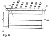
- Fig. 7 and Fig. 8 each show a layer structure of an illumination layer 40. This is shown in the illumination mode with emitted light 18.
- a front electrode layer 42 adjoining this a luminescent layer 44, adjoining this a dielectric layer 46 and adjacent thereto a back electrode layer 48.
- a voltage U L can be applied between front electrode layer 42 and back electrode layer 48.
- a carrier element 50 is shown, which is formed as a transparent substrate layer.
Landscapes
- Physics & Mathematics (AREA)
- Engineering & Computer Science (AREA)
- General Physics & Mathematics (AREA)
- Theoretical Computer Science (AREA)
- Manufacturing & Machinery (AREA)
- Electromagnetism (AREA)
- Electroluminescent Light Sources (AREA)
- Surface Heating Bodies (AREA)
- Resistance Heating (AREA)
Priority Applications (2)
| Application Number | Priority Date | Filing Date | Title |
|---|---|---|---|
| PL17000667T PL3229560T3 (pl) | 2013-09-30 | 2014-09-16 | Element powierzchniowy do świecenia i ogrzewania |
| HRP20191276TT HRP20191276T1 (hr) | 2013-09-30 | 2019-07-16 | Ravni element za rasvjetu i grijanje |
Applications Claiming Priority (2)
| Application Number | Priority Date | Filing Date | Title |
|---|---|---|---|
| DE102013016158.4A DE102013016158B4 (de) | 2013-09-30 | 2013-09-30 | Flächenelement zum Leuchten und Heizen |
| EP14003214.5A EP2854486B1 (de) | 2013-09-30 | 2014-09-16 | Flächenelement zum leuchten und erzeugen sowie speichern von energie |
Related Parent Applications (2)
| Application Number | Title | Priority Date | Filing Date |
|---|---|---|---|
| EP14003214.5A Division-Into EP2854486B1 (de) | 2013-09-30 | 2014-09-16 | Flächenelement zum leuchten und erzeugen sowie speichern von energie |
| EP14003214.5A Division EP2854486B1 (de) | 2013-09-30 | 2014-09-16 | Flächenelement zum leuchten und erzeugen sowie speichern von energie |
Publications (2)
| Publication Number | Publication Date |
|---|---|
| EP3229560A1 EP3229560A1 (de) | 2017-10-11 |
| EP3229560B1 true EP3229560B1 (de) | 2019-05-01 |
Family
ID=51661827
Family Applications (2)
| Application Number | Title | Priority Date | Filing Date |
|---|---|---|---|
| EP17000667.0A Active EP3229560B1 (de) | 2013-09-30 | 2014-09-16 | Flächenelement zum leuchten und heizen |
| EP14003214.5A Active EP2854486B1 (de) | 2013-09-30 | 2014-09-16 | Flächenelement zum leuchten und erzeugen sowie speichern von energie |
Family Applications After (1)
| Application Number | Title | Priority Date | Filing Date |
|---|---|---|---|
| EP14003214.5A Active EP2854486B1 (de) | 2013-09-30 | 2014-09-16 | Flächenelement zum leuchten und erzeugen sowie speichern von energie |
Country Status (6)
| Country | Link |
|---|---|
| EP (2) | EP3229560B1 (pl) |
| DE (1) | DE102013016158B4 (pl) |
| ES (2) | ES2733855T3 (pl) |
| HR (1) | HRP20191276T1 (pl) |
| PL (2) | PL2854486T3 (pl) |
| TR (1) | TR201911261T4 (pl) |
Families Citing this family (3)
| Publication number | Priority date | Publication date | Assignee | Title |
|---|---|---|---|---|
| DE102013016158B4 (de) | 2013-09-30 | 2016-02-18 | Futuredynamics Gmbh | Flächenelement zum Leuchten und Heizen |
| EP3858675B1 (de) * | 2020-01-28 | 2023-08-02 | CT-Coating AG | Warndreieck mit einer folie, haltevorrichtung für das warndreieck, herstellungsverfahren für die folie |
| PL3962233T3 (pl) | 2020-08-25 | 2024-07-22 | CT-Coating AG | Płaski moduł grzewczy, płaski korpus grzewczy, płyta brukowa, system brukowy i sposób wytwarzania modułu grzewczego |
Family Cites Families (23)
| Publication number | Priority date | Publication date | Assignee | Title |
|---|---|---|---|---|
| US6601983B1 (en) * | 2001-07-18 | 2003-08-05 | Vincent A. Runfola | Led vehicular light assembly with heater |
| DE10241728B4 (de) * | 2002-09-10 | 2006-03-16 | Saint-Gobain Glass Deutschland Gmbh | Mehrschichtiges elektrisches beheizbares Flächenelement |
| DE10306720B4 (de) * | 2003-02-18 | 2005-11-24 | Triebold, Klaus-Jörg | Beleuchtungs- und Signalleuchte für Fußgänger und Sport- und Freizeitaktivitäten |
| DE102004031033A1 (de) * | 2004-06-25 | 2006-01-12 | Behr Gmbh & Co. Kg | Vorrichtung zum Beheizen von lichtdurchlässigen Abdeckungen von Strahlen |
| US20060123679A1 (en) * | 2004-12-11 | 2006-06-15 | Debra Scruggs | Battery powered, solar recharged, self contained, universal reflective character display unit |
| DE202006005427U1 (de) * | 2006-04-04 | 2006-06-08 | Emde, Thomas | Beleuchtungsvorrichtung |
| DE102006056271A1 (de) * | 2006-11-27 | 2008-05-29 | Pintsch Bamag Antriebs- Und Verkehrstechnik Gmbh | LED-Leuchte, insbesondere LED-Scheinwerfer und LED-Signallicht, LED-Anordnung für eine Leuchte wie insbesondere einen Scheinwerfer oder ein Signallicht sowie Heizung für eine LED-Leuchte |
| DE102007015472A1 (de) * | 2007-03-30 | 2008-10-02 | Siemens Ag | Aktives Fenster |
| DE202007008574U1 (de) * | 2007-06-14 | 2007-08-16 | Schneider, Ingo F., Dipl.-Ing. | Solares Leuchtdisplay für den Außeneinsatz (Solar Media Modul) |
| US7914162B1 (en) * | 2007-08-23 | 2011-03-29 | Grand General Accessories Manufacturing | LED light assembly having heating board |
| US7810262B2 (en) * | 2008-03-17 | 2010-10-12 | Eli Sadon | Solar powered led illuminated alphanumeric display |
| KR100996503B1 (ko) * | 2008-06-27 | 2010-11-25 | 한국기계연구원 | 전도성 고분자 투명전극을 이용한 oled 및 그 제조방법 |
| US20100214774A1 (en) * | 2009-02-26 | 2010-08-26 | Tzu-Wei Liu | Light emitting device with a solar bulb |
| KR101089507B1 (ko) * | 2009-12-02 | 2011-12-05 | 금호전기주식회사 | 조명 장치 |
| US20110252678A1 (en) * | 2010-04-12 | 2011-10-20 | Dale Jones | Method, apparatus and system for constant led night brightness based on daytime solar charging |
| RU2013147701A (ru) * | 2011-04-05 | 2015-05-10 | Юниверсити Оф Флорида Ресеч Фаундейшен Инк. | Способ и устройство для обеспечения окна, содержащего устройство освещения на основе, по меньшей мере, частично прозрачного органического светоизлучающего устройства с односторонним излучением и чувствительную к ик-излучению фотоэлектрическую панель |
| JP5792806B2 (ja) * | 2011-05-17 | 2015-10-14 | パイオニア株式会社 | 発光装置用ブロック |
| WO2012170609A2 (en) * | 2011-06-07 | 2012-12-13 | Stephen Katsaros | Window-mounted solar light |
| JP2013115356A (ja) * | 2011-11-30 | 2013-06-10 | Panasonic Corp | 発光装置 |
| DE102012204786A1 (de) * | 2012-03-26 | 2013-09-26 | Osram Gmbh | Leuchtvorrichtung mit leuchtstoffkörper auf kühlkörper |
| DE202012005908U1 (de) * | 2012-06-16 | 2012-07-05 | Automotive Lighting Reutlingen Gmbh | Abdeckscheibe für eine Beleuchtungseinrichtung mit einerEnteisungseinrichtung und Beleuchtungseinrichtung mit einer Enteisungseinrichtung |
| DE202012006496U1 (de) * | 2012-07-04 | 2012-08-06 | P.H. Wert-Design E.K. | Leuchte |
| DE102013016158B4 (de) | 2013-09-30 | 2016-02-18 | Futuredynamics Gmbh | Flächenelement zum Leuchten und Heizen |
-
2013
- 2013-09-30 DE DE102013016158.4A patent/DE102013016158B4/de active Active
-
2014
- 2014-09-16 TR TR2019/11261T patent/TR201911261T4/tr unknown
- 2014-09-16 PL PL14003214T patent/PL2854486T3/pl unknown
- 2014-09-16 EP EP17000667.0A patent/EP3229560B1/de active Active
- 2014-09-16 ES ES17000667T patent/ES2733855T3/es active Active
- 2014-09-16 PL PL17000667T patent/PL3229560T3/pl unknown
- 2014-09-16 ES ES14003214.5T patent/ES2639297T3/es active Active
- 2014-09-16 EP EP14003214.5A patent/EP2854486B1/de active Active
-
2019
- 2019-07-16 HR HRP20191276TT patent/HRP20191276T1/hr unknown
Non-Patent Citations (1)
| Title |
|---|
| None * |
Also Published As
| Publication number | Publication date |
|---|---|
| PL2854486T3 (pl) | 2017-12-29 |
| ES2639297T3 (es) | 2017-10-26 |
| PL3229560T3 (pl) | 2019-10-31 |
| DE102013016158B4 (de) | 2016-02-18 |
| DE102013016158A1 (de) | 2015-04-02 |
| ES2733855T3 (es) | 2019-12-03 |
| EP2854486B1 (de) | 2017-06-07 |
| EP2854486A1 (de) | 2015-04-01 |
| TR201911261T4 (tr) | 2019-08-21 |
| EP3229560A1 (de) | 2017-10-11 |
| HRP20191276T1 (hr) | 2019-10-18 |
Similar Documents
| Publication | Publication Date | Title |
|---|---|---|
| DE102006060781B4 (de) | Organisches Leuchtmittel | |
| DE69729867T2 (de) | Elktrolumineszentes system in einer monolithischen struktur | |
| WO2009030701A1 (de) | Elektrolumineszenz-anordnung auf textilen materialien | |
| EP2189042A1 (de) | Kennzeichen mit elektrolumineszenz-leuchteffekt, verfahren zu dessen herstellung | |
| DE10322561A1 (de) | Glaselement mit Lichtrahmen | |
| EP2163136A1 (de) | Anorganisches dickfilm-ac elektrolumineszenzelement mit zumindest zwei einspeisungen und herstellverfahren und anwendung | |
| WO2008003621A1 (de) | 3d-el-hdvf element und herstellungsverfahren und anwendung | |
| EP2854486B1 (de) | Flächenelement zum leuchten und erzeugen sowie speichern von energie | |
| DE102020119072A1 (de) | Beleuchtbare fahrzeugbaugruppe und beleuchtungsverfahren für eine fahrzeugbaugruppe | |
| EP1425990A1 (de) | Einrichtungselement mit selbstleuchtenden Sichtflächen und Verfahren zur Herstellung | |
| DE20005419U1 (de) | Elektrolumineszenz-Leuchtkörper | |
| DE102014104230A1 (de) | Strahlungsemittierendes Bauteil und Verfahren zur Herstellung eines strahlungsemittierenden Bauteils | |
| EP2334151A1 (de) | Verfahren zur Herstellung eines Elektrolumineszenz-Elements mittels Sprühapplikation auf beliebig geformten Gegenständen | |
| EP2215892A1 (de) | Mindestens einschichtiges anorganisches dickfilm-ac elektrolumineszenz-system mit unterschiedlich konturierten und weitgehend transparenten leitschichten, verfahren zu dessen herstellung und dessen verwendung | |
| DE102008057606A1 (de) | Kombinationsleuchte | |
| DE102010002885B4 (de) | Beleuchtungseinheit mit organischer Leuchtdiode, deren Verwendung als Display sowie Verfahren zur Herstellung der Beleuchtungseinheit | |
| EP1738614B1 (de) | Mehrfarb-elektrolumineszenz-element | |
| EP1993326A1 (de) | Teilchen mit Nanostrukturen enthaltendes Elektrolumineszenzelement | |
| DE102017207482A1 (de) | Elektrolumineszierendes übertragungslaminat und hieraus erlangte elektrolumineszierende übertragungseinheit | |
| EP2018793B1 (de) | Verfahren zum herstellen einer elektrolumineszenzanordnung sowie nach einem solchen verfahren hergestellte elektrolumineszenzanordnung | |
| EP1152643B1 (de) | Anzeigevorrichtung mit mindestens einer elektrolumineszierenden Fläche | |
| EP2924759B1 (de) | Leuchtmodul und herstellungsverfahren für ein leuchtmodul | |
| DE202009016123U1 (de) | Elektrolumineszierender Folienverbund mit einem Schutzfolienlaminat | |
| WO2005104625A1 (de) | Beleuchtungsschichtsystem und verfahren zur herstellung desselben | |
| CN2353011Y (zh) | 带发光屏的可透视广告贴 |
Legal Events
| Date | Code | Title | Description |
|---|---|---|---|
| PUAI | Public reference made under article 153(3) epc to a published international application that has entered the european phase |
Free format text: ORIGINAL CODE: 0009012 |
|
| STAA | Information on the status of an ep patent application or granted ep patent |
Free format text: STATUS: THE APPLICATION HAS BEEN PUBLISHED |
|
| AC | Divisional application: reference to earlier application |
Ref document number: 2854486 Country of ref document: EP Kind code of ref document: P |
|
| AK | Designated contracting states |
Kind code of ref document: A1 Designated state(s): AL AT BE BG CH CY CZ DE DK EE ES FI FR GB GR HR HU IE IS IT LI LT LU LV MC MK MT NL NO PL PT RO RS SE SI SK SM TR |
|
| STAA | Information on the status of an ep patent application or granted ep patent |
Free format text: STATUS: REQUEST FOR EXAMINATION WAS MADE |
|
| 17P | Request for examination filed |
Effective date: 20180409 |
|
| RBV | Designated contracting states (corrected) |
Designated state(s): AL AT BE BG CH CY CZ DE DK EE ES FI FR GB GR HR HU IE IS IT LI LT LU LV MC MK MT NL NO PL PT RO RS SE SI SK SM TR |
|
| STAA | Information on the status of an ep patent application or granted ep patent |
Free format text: STATUS: EXAMINATION IS IN PROGRESS |
|
| 17Q | First examination report despatched |
Effective date: 20180817 |
|
| GRAP | Despatch of communication of intention to grant a patent |
Free format text: ORIGINAL CODE: EPIDOSNIGR1 |
|
| STAA | Information on the status of an ep patent application or granted ep patent |
Free format text: STATUS: GRANT OF PATENT IS INTENDED |
|
| INTG | Intention to grant announced |
Effective date: 20181211 |
|
| GRAS | Grant fee paid |
Free format text: ORIGINAL CODE: EPIDOSNIGR3 |
|
| GRAA | (expected) grant |
Free format text: ORIGINAL CODE: 0009210 |
|
| STAA | Information on the status of an ep patent application or granted ep patent |
Free format text: STATUS: THE PATENT HAS BEEN GRANTED |
|
| AC | Divisional application: reference to earlier application |
Ref document number: 2854486 Country of ref document: EP Kind code of ref document: P |
|
| AK | Designated contracting states |
Kind code of ref document: B1 Designated state(s): AL AT BE BG CH CY CZ DE DK EE ES FI FR GB GR HR HU IE IS IT LI LT LU LV MC MK MT NL NO PL PT RO RS SE SI SK SM TR |
|
| REG | Reference to a national code |
Ref country code: GB Ref legal event code: FG4D Free format text: NOT ENGLISH |
|
| REG | Reference to a national code |
Ref country code: CH Ref legal event code: EP Ref country code: AT Ref legal event code: REF Ref document number: 1128669 Country of ref document: AT Kind code of ref document: T Effective date: 20190515 |
|
| REG | Reference to a national code |
Ref country code: DE Ref legal event code: R096 Ref document number: 502014011621 Country of ref document: DE |
|
| REG | Reference to a national code |
Ref country code: IE Ref legal event code: FG4D Free format text: LANGUAGE OF EP DOCUMENT: GERMAN |
|
| REG | Reference to a national code |
Ref country code: CH Ref legal event code: NV Representative=s name: ROTTMANN, ZIMMERMANN + PARTNER AG, CH |
|
| REG | Reference to a national code |
Ref country code: HR Ref legal event code: TUEP Ref document number: P20191276 Country of ref document: HR |
|
| REG | Reference to a national code |
Ref country code: NL Ref legal event code: FP |
|
| REG | Reference to a national code |
Ref country code: LT Ref legal event code: MG4D |
|
| REG | Reference to a national code |
Ref country code: HR Ref legal event code: ODRP Ref document number: P20191276 Country of ref document: HR Payment date: 20190717 Year of fee payment: 6 |
|
| REG | Reference to a national code |
Ref country code: HR Ref legal event code: T1PR Ref document number: P20191276 Country of ref document: HR |
|
| PG25 | Lapsed in a contracting state [announced via postgrant information from national office to epo] |
Ref country code: FI Free format text: LAPSE BECAUSE OF FAILURE TO SUBMIT A TRANSLATION OF THE DESCRIPTION OR TO PAY THE FEE WITHIN THE PRESCRIBED TIME-LIMIT Effective date: 20190501 Ref country code: AL Free format text: LAPSE BECAUSE OF FAILURE TO SUBMIT A TRANSLATION OF THE DESCRIPTION OR TO PAY THE FEE WITHIN THE PRESCRIBED TIME-LIMIT Effective date: 20190501 Ref country code: PT Free format text: LAPSE BECAUSE OF FAILURE TO SUBMIT A TRANSLATION OF THE DESCRIPTION OR TO PAY THE FEE WITHIN THE PRESCRIBED TIME-LIMIT Effective date: 20190901 Ref country code: NO Free format text: LAPSE BECAUSE OF FAILURE TO SUBMIT A TRANSLATION OF THE DESCRIPTION OR TO PAY THE FEE WITHIN THE PRESCRIBED TIME-LIMIT Effective date: 20190801 Ref country code: SE Free format text: LAPSE BECAUSE OF FAILURE TO SUBMIT A TRANSLATION OF THE DESCRIPTION OR TO PAY THE FEE WITHIN THE PRESCRIBED TIME-LIMIT Effective date: 20190501 Ref country code: LT Free format text: LAPSE BECAUSE OF FAILURE TO SUBMIT A TRANSLATION OF THE DESCRIPTION OR TO PAY THE FEE WITHIN THE PRESCRIBED TIME-LIMIT Effective date: 20190501 |
|
| PG25 | Lapsed in a contracting state [announced via postgrant information from national office to epo] |
Ref country code: LV Free format text: LAPSE BECAUSE OF FAILURE TO SUBMIT A TRANSLATION OF THE DESCRIPTION OR TO PAY THE FEE WITHIN THE PRESCRIBED TIME-LIMIT Effective date: 20190501 Ref country code: RS Free format text: LAPSE BECAUSE OF FAILURE TO SUBMIT A TRANSLATION OF THE DESCRIPTION OR TO PAY THE FEE WITHIN THE PRESCRIBED TIME-LIMIT Effective date: 20190501 Ref country code: BG Free format text: LAPSE BECAUSE OF FAILURE TO SUBMIT A TRANSLATION OF THE DESCRIPTION OR TO PAY THE FEE WITHIN THE PRESCRIBED TIME-LIMIT Effective date: 20190801 |
|
| REG | Reference to a national code |
Ref country code: ES Ref legal event code: FG2A Ref document number: 2733855 Country of ref document: ES Kind code of ref document: T3 Effective date: 20191203 |
|
| PG25 | Lapsed in a contracting state [announced via postgrant information from national office to epo] |
Ref country code: IS Free format text: LAPSE BECAUSE OF FAILURE TO SUBMIT A TRANSLATION OF THE DESCRIPTION OR TO PAY THE FEE WITHIN THE PRESCRIBED TIME-LIMIT Effective date: 20190901 |
|
| PG25 | Lapsed in a contracting state [announced via postgrant information from national office to epo] |
Ref country code: CZ Free format text: LAPSE BECAUSE OF FAILURE TO SUBMIT A TRANSLATION OF THE DESCRIPTION OR TO PAY THE FEE WITHIN THE PRESCRIBED TIME-LIMIT Effective date: 20190501 Ref country code: SK Free format text: LAPSE BECAUSE OF FAILURE TO SUBMIT A TRANSLATION OF THE DESCRIPTION OR TO PAY THE FEE WITHIN THE PRESCRIBED TIME-LIMIT Effective date: 20190501 Ref country code: DK Free format text: LAPSE BECAUSE OF FAILURE TO SUBMIT A TRANSLATION OF THE DESCRIPTION OR TO PAY THE FEE WITHIN THE PRESCRIBED TIME-LIMIT Effective date: 20190501 Ref country code: EE Free format text: LAPSE BECAUSE OF FAILURE TO SUBMIT A TRANSLATION OF THE DESCRIPTION OR TO PAY THE FEE WITHIN THE PRESCRIBED TIME-LIMIT Effective date: 20190501 Ref country code: RO Free format text: LAPSE BECAUSE OF FAILURE TO SUBMIT A TRANSLATION OF THE DESCRIPTION OR TO PAY THE FEE WITHIN THE PRESCRIBED TIME-LIMIT Effective date: 20190501 |
|
| REG | Reference to a national code |
Ref country code: DE Ref legal event code: R097 Ref document number: 502014011621 Country of ref document: DE |
|
| PG25 | Lapsed in a contracting state [announced via postgrant information from national office to epo] |
Ref country code: IT Free format text: LAPSE BECAUSE OF FAILURE TO SUBMIT A TRANSLATION OF THE DESCRIPTION OR TO PAY THE FEE WITHIN THE PRESCRIBED TIME-LIMIT Effective date: 20190501 Ref country code: SM Free format text: LAPSE BECAUSE OF FAILURE TO SUBMIT A TRANSLATION OF THE DESCRIPTION OR TO PAY THE FEE WITHIN THE PRESCRIBED TIME-LIMIT Effective date: 20190501 |
|
| PLBE | No opposition filed within time limit |
Free format text: ORIGINAL CODE: 0009261 |
|
| STAA | Information on the status of an ep patent application or granted ep patent |
Free format text: STATUS: NO OPPOSITION FILED WITHIN TIME LIMIT |
|
| 26N | No opposition filed |
Effective date: 20200204 |
|
| PG25 | Lapsed in a contracting state [announced via postgrant information from national office to epo] |
Ref country code: SI Free format text: LAPSE BECAUSE OF FAILURE TO SUBMIT A TRANSLATION OF THE DESCRIPTION OR TO PAY THE FEE WITHIN THE PRESCRIBED TIME-LIMIT Effective date: 20190501 Ref country code: MC Free format text: LAPSE BECAUSE OF FAILURE TO SUBMIT A TRANSLATION OF THE DESCRIPTION OR TO PAY THE FEE WITHIN THE PRESCRIBED TIME-LIMIT Effective date: 20190501 |
|
| PG25 | Lapsed in a contracting state [announced via postgrant information from national office to epo] |
Ref country code: LU Free format text: LAPSE BECAUSE OF NON-PAYMENT OF DUE FEES Effective date: 20190916 Ref country code: IE Free format text: LAPSE BECAUSE OF NON-PAYMENT OF DUE FEES Effective date: 20190916 |
|
| REG | Reference to a national code |
Ref country code: HR Ref legal event code: ODRP Ref document number: P20191276 Country of ref document: HR Payment date: 20200904 Year of fee payment: 7 |
|
| PG25 | Lapsed in a contracting state [announced via postgrant information from national office to epo] |
Ref country code: CY Free format text: LAPSE BECAUSE OF FAILURE TO SUBMIT A TRANSLATION OF THE DESCRIPTION OR TO PAY THE FEE WITHIN THE PRESCRIBED TIME-LIMIT Effective date: 20190501 |
|
| PG25 | Lapsed in a contracting state [announced via postgrant information from national office to epo] |
Ref country code: GR Free format text: LAPSE BECAUSE OF FAILURE TO SUBMIT A TRANSLATION OF THE DESCRIPTION OR TO PAY THE FEE WITHIN THE PRESCRIBED TIME-LIMIT Effective date: 20190501 |
|
| PG25 | Lapsed in a contracting state [announced via postgrant information from national office to epo] |
Ref country code: MT Free format text: LAPSE BECAUSE OF FAILURE TO SUBMIT A TRANSLATION OF THE DESCRIPTION OR TO PAY THE FEE WITHIN THE PRESCRIBED TIME-LIMIT Effective date: 20190501 Ref country code: HU Free format text: LAPSE BECAUSE OF FAILURE TO SUBMIT A TRANSLATION OF THE DESCRIPTION OR TO PAY THE FEE WITHIN THE PRESCRIBED TIME-LIMIT; INVALID AB INITIO Effective date: 20140916 |
|
| REG | Reference to a national code |
Ref country code: HR Ref legal event code: ODRP Ref document number: P20191276 Country of ref document: HR Payment date: 20210907 Year of fee payment: 8 |
|
| PG25 | Lapsed in a contracting state [announced via postgrant information from national office to epo] |
Ref country code: MK Free format text: LAPSE BECAUSE OF FAILURE TO SUBMIT A TRANSLATION OF THE DESCRIPTION OR TO PAY THE FEE WITHIN THE PRESCRIBED TIME-LIMIT Effective date: 20190501 |
|
| REG | Reference to a national code |
Ref country code: HR Ref legal event code: ODRP Ref document number: P20191276 Country of ref document: HR Payment date: 20221011 Year of fee payment: 9 |
|
| REG | Reference to a national code |
Ref country code: HR Ref legal event code: ODRP Ref document number: P20191276 Country of ref document: HR Payment date: 20230913 Year of fee payment: 10 |
|
| REG | Reference to a national code |
Ref country code: HR Ref legal event code: ODRP Ref document number: P20191276 Country of ref document: HR Payment date: 20240910 Year of fee payment: 11 |
|
| REG | Reference to a national code |
Ref country code: CH Ref legal event code: U11 Free format text: ST27 STATUS EVENT CODE: U-0-0-U10-U11 (AS PROVIDED BY THE NATIONAL OFFICE) Effective date: 20251027 |
|
| PGFP | Annual fee paid to national office [announced via postgrant information from national office to epo] |
Ref country code: NL Payment date: 20251017 Year of fee payment: 12 |
|
| REG | Reference to a national code |
Ref country code: HR Ref legal event code: ODRP Ref document number: P20191276 Country of ref document: HR Payment date: 20251105 Year of fee payment: 12 |
|
| PGFP | Annual fee paid to national office [announced via postgrant information from national office to epo] |
Ref country code: DE Payment date: 20251013 Year of fee payment: 12 |
|
| PGFP | Annual fee paid to national office [announced via postgrant information from national office to epo] |
Ref country code: GB Payment date: 20251024 Year of fee payment: 12 |
|
| PGFP | Annual fee paid to national office [announced via postgrant information from national office to epo] |
Ref country code: AT Payment date: 20251021 Year of fee payment: 12 |
|
| PGFP | Annual fee paid to national office [announced via postgrant information from national office to epo] |
Ref country code: HR Payment date: 20251105 Year of fee payment: 12 Ref country code: FR Payment date: 20251017 Year of fee payment: 12 |
|
| PGFP | Annual fee paid to national office [announced via postgrant information from national office to epo] |
Ref country code: TR Payment date: 20251110 Year of fee payment: 12 Ref country code: BE Payment date: 20251016 Year of fee payment: 12 |
|
| PGFP | Annual fee paid to national office [announced via postgrant information from national office to epo] |
Ref country code: CH Payment date: 20251024 Year of fee payment: 12 |
|
| PGFP | Annual fee paid to national office [announced via postgrant information from national office to epo] |
Ref country code: PL Payment date: 20251106 Year of fee payment: 12 |
|
| PGFP | Annual fee paid to national office [announced via postgrant information from national office to epo] |
Ref country code: ES Payment date: 20251020 Year of fee payment: 12 |
|
| REG | Reference to a national code |
Ref country code: CH Ref legal event code: R17 Free format text: ST27 STATUS EVENT CODE: U-0-0-R10-R17 (AS PROVIDED BY THE NATIONAL OFFICE) Effective date: 20260410 |