EP3223321A1 - Light-emitting device - Google Patents
Light-emitting device Download PDFInfo
- Publication number
- EP3223321A1 EP3223321A1 EP17161739.2A EP17161739A EP3223321A1 EP 3223321 A1 EP3223321 A1 EP 3223321A1 EP 17161739 A EP17161739 A EP 17161739A EP 3223321 A1 EP3223321 A1 EP 3223321A1
- Authority
- EP
- European Patent Office
- Prior art keywords
- layered structure
- disposed
- protective film
- semiconductor layered
- light
- Prior art date
- Legal status (The legal status is an assumption and is not a legal conclusion. Google has not performed a legal analysis and makes no representation as to the accuracy of the status listed.)
- Granted
Links
Images


Classifications
-
- H—ELECTRICITY
- H10—SEMICONDUCTOR DEVICES; ELECTRIC SOLID-STATE DEVICES NOT OTHERWISE PROVIDED FOR
- H10H—INORGANIC LIGHT-EMITTING SEMICONDUCTOR DEVICES HAVING POTENTIAL BARRIERS
- H10H20/00—Individual inorganic light-emitting semiconductor devices having potential barriers, e.g. light-emitting diodes [LED]
- H10H20/80—Constructional details
- H10H20/83—Electrodes
- H10H20/831—Electrodes characterised by their shape
-
- H—ELECTRICITY
- H10—SEMICONDUCTOR DEVICES; ELECTRIC SOLID-STATE DEVICES NOT OTHERWISE PROVIDED FOR
- H10H—INORGANIC LIGHT-EMITTING SEMICONDUCTOR DEVICES HAVING POTENTIAL BARRIERS
- H10H20/00—Individual inorganic light-emitting semiconductor devices having potential barriers, e.g. light-emitting diodes [LED]
- H10H20/80—Constructional details
- H10H20/83—Electrodes
-
- H—ELECTRICITY
- H10—SEMICONDUCTOR DEVICES; ELECTRIC SOLID-STATE DEVICES NOT OTHERWISE PROVIDED FOR
- H10H—INORGANIC LIGHT-EMITTING SEMICONDUCTOR DEVICES HAVING POTENTIAL BARRIERS
- H10H20/00—Individual inorganic light-emitting semiconductor devices having potential barriers, e.g. light-emitting diodes [LED]
- H10H20/01—Manufacture or treatment
- H10H20/032—Manufacture or treatment of electrodes
-
- H—ELECTRICITY
- H10—SEMICONDUCTOR DEVICES; ELECTRIC SOLID-STATE DEVICES NOT OTHERWISE PROVIDED FOR
- H10H—INORGANIC LIGHT-EMITTING SEMICONDUCTOR DEVICES HAVING POTENTIAL BARRIERS
- H10H20/00—Individual inorganic light-emitting semiconductor devices having potential barriers, e.g. light-emitting diodes [LED]
- H10H20/01—Manufacture or treatment
- H10H20/036—Manufacture or treatment of packages
- H10H20/0364—Manufacture or treatment of packages of interconnections
-
- H—ELECTRICITY
- H10—SEMICONDUCTOR DEVICES; ELECTRIC SOLID-STATE DEVICES NOT OTHERWISE PROVIDED FOR
- H10H—INORGANIC LIGHT-EMITTING SEMICONDUCTOR DEVICES HAVING POTENTIAL BARRIERS
- H10H20/00—Individual inorganic light-emitting semiconductor devices having potential barriers, e.g. light-emitting diodes [LED]
- H10H20/80—Constructional details
- H10H20/81—Bodies
-
- H—ELECTRICITY
- H10—SEMICONDUCTOR DEVICES; ELECTRIC SOLID-STATE DEVICES NOT OTHERWISE PROVIDED FOR
- H10H—INORGANIC LIGHT-EMITTING SEMICONDUCTOR DEVICES HAVING POTENTIAL BARRIERS
- H10H20/00—Individual inorganic light-emitting semiconductor devices having potential barriers, e.g. light-emitting diodes [LED]
- H10H20/80—Constructional details
- H10H20/81—Bodies
- H10H20/819—Bodies characterised by their shape, e.g. curved or truncated substrates
- H10H20/82—Roughened surfaces, e.g. at the interface between epitaxial layers
-
- H—ELECTRICITY
- H10—SEMICONDUCTOR DEVICES; ELECTRIC SOLID-STATE DEVICES NOT OTHERWISE PROVIDED FOR
- H10H—INORGANIC LIGHT-EMITTING SEMICONDUCTOR DEVICES HAVING POTENTIAL BARRIERS
- H10H20/00—Individual inorganic light-emitting semiconductor devices having potential barriers, e.g. light-emitting diodes [LED]
- H10H20/80—Constructional details
- H10H20/83—Electrodes
- H10H20/832—Electrodes characterised by their material
-
- H—ELECTRICITY
- H10—SEMICONDUCTOR DEVICES; ELECTRIC SOLID-STATE DEVICES NOT OTHERWISE PROVIDED FOR
- H10H—INORGANIC LIGHT-EMITTING SEMICONDUCTOR DEVICES HAVING POTENTIAL BARRIERS
- H10H20/00—Individual inorganic light-emitting semiconductor devices having potential barriers, e.g. light-emitting diodes [LED]
- H10H20/80—Constructional details
- H10H20/83—Electrodes
- H10H20/832—Electrodes characterised by their material
- H10H20/835—Reflective materials
-
- H—ELECTRICITY
- H10—SEMICONDUCTOR DEVICES; ELECTRIC SOLID-STATE DEVICES NOT OTHERWISE PROVIDED FOR
- H10H—INORGANIC LIGHT-EMITTING SEMICONDUCTOR DEVICES HAVING POTENTIAL BARRIERS
- H10H20/00—Individual inorganic light-emitting semiconductor devices having potential barriers, e.g. light-emitting diodes [LED]
- H10H20/80—Constructional details
- H10H20/84—Coatings, e.g. passivation layers or antireflective coatings
-
- H—ELECTRICITY
- H10—SEMICONDUCTOR DEVICES; ELECTRIC SOLID-STATE DEVICES NOT OTHERWISE PROVIDED FOR
- H10H—INORGANIC LIGHT-EMITTING SEMICONDUCTOR DEVICES HAVING POTENTIAL BARRIERS
- H10H20/00—Individual inorganic light-emitting semiconductor devices having potential barriers, e.g. light-emitting diodes [LED]
- H10H20/80—Constructional details
- H10H20/85—Packages
- H10H20/857—Interconnections, e.g. lead-frames, bond wires or solder balls
-
- H—ELECTRICITY
- H10—SEMICONDUCTOR DEVICES; ELECTRIC SOLID-STATE DEVICES NOT OTHERWISE PROVIDED FOR
- H10H—INORGANIC LIGHT-EMITTING SEMICONDUCTOR DEVICES HAVING POTENTIAL BARRIERS
- H10H29/00—Integrated devices, or assemblies of multiple devices, comprising at least one light-emitting semiconductor element covered by group H10H20/00
- H10H29/10—Integrated devices comprising at least one light-emitting semiconductor component covered by group H10H20/00
-
- H—ELECTRICITY
- H10—SEMICONDUCTOR DEVICES; ELECTRIC SOLID-STATE DEVICES NOT OTHERWISE PROVIDED FOR
- H10H—INORGANIC LIGHT-EMITTING SEMICONDUCTOR DEVICES HAVING POTENTIAL BARRIERS
- H10H20/00—Individual inorganic light-emitting semiconductor devices having potential barriers, e.g. light-emitting diodes [LED]
- H10H20/80—Constructional details
- H10H20/81—Bodies
- H10H20/822—Materials of the light-emitting regions
- H10H20/824—Materials of the light-emitting regions comprising only Group III-V materials, e.g. GaP
- H10H20/825—Materials of the light-emitting regions comprising only Group III-V materials, e.g. GaP containing nitrogen, e.g. GaN
Definitions
- the present disclosure relates to a light-emitting device.
- Japanese Laid-Open Patent Publication No. 2014-236070 discloses a light-emitting device in which a bonding electrode is disposed on an upper surface side of a semiconductor layered structure, a metal electrode is disposed on a lower surface side of the semiconductor layered structure, and a protective film is disposed on a surface of the semiconductor layered structure.
- a protective film with a uniform thickness is disposed on an upper surface of the semiconductor layered structure.
- the semiconductor layered structure may be deteriorated. If the thickness of the protective film is increased, deterioration of the semiconductor layered structure can be suppressed but, on the other hand, light from the semiconductor layered structure is easily absorbed by the protective film, so that the light extraction efficiency may be decreased.
- one of the objects of the present disclosure is to provide a light-emitting device in which deterioration of the semiconductor layered structure is reduced and which has a high light extraction efficiency.
- a light-emitting device includes: a semiconductor layered structure; an upper electrode disposed on a portion of an upper surface of the semiconductor layered structure; a lower electrode having light reflectivity and disposed on a lower surface of the semiconductor layered structure in a region a region of spaced from a region directly under the upper electrode; and a protective film disposed to be continuous on a surface of the upper electrode and on the upper surface of the semiconductor layered structure.
- a portion of the protective film in a region directly above the lower electrode has a thickness smaller than a thickness of a portion of the protective film that is continuous on the surface of the upper electrode and on the upper surface of the semiconductor layered structure in a region in the vicinity of a region in which the upper electrode is disposed.
- the above-described configuration can realize a light-emitting device in which deterioration of the semiconductor layered structure is reduced and which has a high light extraction efficiency.
- FIG. 1 is a top view of a light-emitting device 100 according to the present embodiment.
- FIG. 2 is a schematic partial cross-sectional view for illustrating the configuration of the light-emitting device 100 .
- FIG. 3 is a schematic top view for illustrating a region of the light-emitting device 100 in which members disposed on the upper and lower surfaces of a semiconductor layered structure 10 are disposed.
- FIG. 4 is a partial cross-sectional view for illustrating the configuration of a light-emitting device 200 according to a second embodiment.
- FIG. 5 is a partial cross-sectional view for illustrating the configuration of a light-emitting device 100 according to the first embodiment.
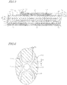
- FIG. 6 is an enlarged top view of a region indicated by R1 in FIG. 3 , schematically showing the configuration of the light-emitting device 100 according to the first embodiment.
- the hatched region indicates a region in which a lower electrode 12 is disposed in a top view, and does not indicate a cross
- the light-emitting device 100 includes a semiconductor layered structure 10 , an upper electrode 11 disposed on a portion of the upper surface of the semiconductor layered structure 10 , a lower electrode 12 having light reflectivity and disposed on the lower surface of the semiconductor layered structure 10 in a region spaced from a region directly under the upper electrode 11 , and a protective film 13 disposed to be continuous on a surface of the upper electrode 11 and on the upper surface of the semiconductor layered structure 10 .
- a portion of the protective film 13 in a region 12R directly above the lower electrode 12 has a thickness smaller than a thickness of a portion of the protective film 13 disposed continuously on the surface of the upper electrode 11 and on a portion of the upper surface of the semiconductor layered structure 10 in the vicinity of a region in which the upper electrode 11 is disposed.
- the upper surface of the semiconductor layered structure 10 serves as a surface from which light is primarily extracted. Surfaces of the semiconductor layered structure 10 are covered with a transparent protective film 13 for reducing deterioration of the semiconductor layered structure 10 . However, a portion of light from the semiconductor layered structure 10 is absorbed by the protective film 13 , so that the output can be decreased.
- the upper electrode 11 and the lower electrode 12 are disposed in different regions in a top view. Therefore, when viewed from the top surface, the region directly above the lower electrode 12 tends to emit intense light. Thus, in the region directly above the lower electrode 12 , a portion of the light is easily absorbed by the protective film.
- moisture may enter through an opening defined in the protective film 13 , through which the power is to be supplied from an external device, and a portion of the protective film 13 having a small thickness.
- vicinity regions 13R current density in regions in the vicinity of the regions in which the upper electrodes 11 are disposed
- optical density in this region is increased. Due to moisture and high optical density as described above, portions of the semiconductor layered structure 10 in the vicinity regions 13R may be easily oxidized and deteriorated.
- the thickness of a portion of the protective film 13 on the upper surface of the semiconductor layered structure 10 in the region 12R directly above the lower electrode 12 is reduced, which allows for reducing absorption of light by the protective film 13 , so that the light extraction efficiency is improved. Meanwhile, the thickness of a portion of the protective film 13 on the surface of the upper electrode 11 and in the vicinity regions 13R is increased. With this configuration, in the vicinity regions 13R , where the semiconductor layered structure 10 tends to be easily deteriorated, deterioration of the semiconductor layered structure 10 can be reduced. That is, in the present embodiment, the light extraction efficiency can be improved while the reliability of the light-emitting device 100 is maintained.
- the semiconductor layered structure 10 includes a p-side semiconductor layer 10p , an active layer 10a and a n-side semiconductor layer 10n in this order from the substrate 16 side, which is the lower side of the light-emitting device 100 , as shown in FIG. 2 .
- the semiconductor layered structure 10 has a generally square shape with each side of about 2 mm.
- a nitride semiconductor such as, for example, In X Al Y Ga 1-X-Y N (0 ⁇ X, 0 ⁇ Y, X+Y ⁇ 1) can be used.
- the upper surface of the n-side semiconductor layer 10n of the semiconductor layered structure 10 can be a roughened surface. With the upper surface that is roughened, the light extraction efficiency can be improved.
- each of the protrusions preferably has a height of 0.2 to 3.0 ⁇ m, more preferably has a height of 0.4 to 1.5 ⁇ m, for appropriately improving the light extraction efficiency.
- the upper electrodes 11 are disposed on portions of the upper surface of the semiconductor layered structure 10 and are electrically connected with the n-side semiconductor layer 10n as shown in FIG. 2 . That is, in the present embodiment, the upper electrodes 11 function as the n-electrode.
- the upper electrodes 11 each includes an external connecting portion 11a and an extended portion 11b extending from the external connecting portion 11a .
- the external connecting portion 11a is a region to be connected with an external member, such as a wire.
- the extended portion 11b is an electrode for diffusing an electric current supplied to the external connecting portion 11a over a larger area.
- a plurality of external connecting portions 11a are disposed on the upper surface of the semiconductor layered structure 10 , the extended portion 11b is disposed at each of the external connecting portions 11a .
- a metal such as Ni, Au, W, Pt, Al, Rh, Ti, or the like, can be used.
- the lower electrode 12 is disposed on a portion of the lower surface of the semiconductor layered structure 10 and is electrically connected with the p-side semiconductor layer 10p . That is, in the present embodiment, the lower electrode 12 functions as the p-electrode. In FIG. 3 , the lower electrode 12 is disposed in a region hatched with oblique lines sloping upward to the left. As can be understood from FIG. 3 , the lower electrode 12 is disposed on the lower surface of the semiconductor layered structure 10 in a region which is spaced from a region directly under the upper electrodes 11 .
- the lower electrode 12 is configured to reflect light from the semiconductor layered structure 10 toward the upper surface side, which allows for improving the light extraction efficiency of the light-emitting device 100 .
- the lower electrode 12 is preferably made of a metal which has a high reflectance.
- a metal such as Ag, Al, or an alloy whose main component is one or more of these metals can be used.
- the protective film 13 has the function of protecting the light-emitting device 100 .
- the protective film 13 is disposed on a portion of the upper surface of the semiconductor layered structure 10 on which the upper electrodes 11 are not disposed, and on a surface of each of the upper electrodes 11 .
- the protective film 13 is not disposed on a portion of each external connecting portion 11a .
- an electrically-conductive wire, or the like is bonded for electrical connection with an external power supply.
- a portion of the protective film 13 in the region 12R directly above the lower electrode 12 has a thickness smaller than a thickness of a portion of the protective film 13 continuous on the surface of each of the upper electrodes 11 and on the upper surface of the semiconductor layered structure 10 in the vicinity regions 13R .
- the portion of the protective film 13 disposed continuously on the surface of each of the upper electrodes 11 and the upper surface of the semiconductor layered structure 10 in the vicinity regions 13R has a thickness (for example, Ta and Tb shown in Fig. 5 ) greater than the thickness (for example, Tc shown in Fig. 5 ) of a portion of the protective film 13 in the region 12R directly above the lower electrode 12 .
- the "thickness" of the protective film 13 used in the present specification refers to a dimension of the protective film in a direction perpendicular to a surface of each member on which the protective film 13 is to be formed.
- a thickness of the protective film 13 is reduced only in the region directly above the lower electrode 12 . That is, in the other regions, the protective film 13 has a relatively large thickness. With this arrangement, the light extraction efficiency can be further improved.
- the protective film 13 has a relatively large thickness at the periphery of the semiconductor layered structure 10 as shown in FIG. 2 .
- a portion of the protective film 13 at the periphery of the semiconductor layered structure 10 , particularly a portion of the protective film 13 over the upper and lateral surfaces of the semiconductor layered structure 10 is likely to have a smaller thickness.
- forming protective film 13 to have a relatively large thickness at the periphery of the semiconductor layered structure 10 allows for protecting the semiconductor layered structure 10 , so that reliability can be further improved.
- a portion of the protective film 13 in the region 12R directly above the lower electrode 12 preferably has a thickness of 40% or less, more preferably 35% or less, of the thickness of a portion of the protective film 13 on the surface of each of the upper electrodes 11 and on the upper surface of the semiconductor layered structure 10 in the vicinity regions 13R .
- the thickness of a portion of the protective film 13 in the region directly above the lower electrode 12 is 0.2 ⁇ m, while the thickness of a portion of the protective film 13 continuous on the surface of each of the upper electrode 11 and the upper surface of the semiconductor layered structure 10 in the vicinity regions 13R is 0.7 ⁇ m.
- a portion of the protective film 13 in the region 12R directly above the lower electrode 12 preferably has a thickness of 0.2 to 0.3 ⁇ m. With this arrangement, absorption of light from the semiconductor layered structure 10 can be further reduced while the protective film 13 has the protection function to some extent.
- a portion of the protective film 13 continuous on the surface of each of the upper electrode 11 and the upper surface of the semiconductor layered structure 10 in the vicinity regions 13R preferably has a thickness of 0.5 to 1.0 ⁇ m. With this arrangement, moisture does not easily pass through the protective film 13 and reach the semiconductor layered structure 10 . Therefore, deterioration of the semiconductor layered structure 10 can be reduced. Further, the semiconductor layered structure 10 can be protected from external shocks and the like, so that the reliability of the light-emitting device 100 can be improved.
- the protective film 13 is disposed to be continuous on a surface of the extended portion 11b and on the upper surface of the semiconductor layered structure 10 including a region in the vicinity of a region on which the extended portion 11b is disposed.
- a portion of the protective film 13 on a surface of the extended portion 11b and a portion of the upper surface of the semiconductor layered structure 10 in the region in the vicinity of the region on which the extended portion 11b is disposed has a thickness greater than the thickness of a portion of the protective film 13 in the region 12R directly above the lower electrode 12 as shown in FIG. 5 .
- each of the upper electrode 11 preferably includes a first upper electrode 111 disposed on a portion of the upper surface of the semiconductor layered structure 10 and a second upper electrode 112 disposed on the first upper electrode 111 .
- an end portion of the protective film 13 is preferably disposed between the first upper electrode 111 and the second upper electrode 112 .
- entry of moisture via the gap between the first upper electrode 111 and the protective film 13 can be reduced, so that deterioration of the semiconductor layered structure 10 can also be reduced, as compared with the case where the second upper electrode 112 is not disposed.
- such a multilayer structure may be employed only in a region to be the external connecting portion 11a . With this arrangement, absorption of light by the upper electrodes 11 is reduced, so that reduction in output can be reduced.
- the periphery of each of the vicinity regions 13R in the vicinity of the regions on which the upper electrodes 11 are disposed is preferably located spaced from an edge of respective one of the upper electrodes 11 by a distance in a range of 15 ⁇ m to 30 ⁇ m. That is, the periphery of a region of the protective film 13 having a thickness greater than a thickness of a portion of the protective film 13 in the region directly above the lower electrode 12 is preferably positioned in a region spaced from an edge of respective one of the upper electrodes 11 by a distance in a range of 15 ⁇ m to 30 ⁇ m.
- vicinity regions 13R each having the periphery located spaced from the edge of respective one of the upper electrodes 11 by a distance of 15 ⁇ m or more With the vicinity regions 13R each having the periphery located spaced from the edge of respective one of the upper electrodes 11 by a distance of 15 ⁇ m or more, deterioration of the semiconductor layered structure 10 in the vicinity regions 13R can be suppressed. Further, with the vicinity regions 13R each having the periphery located spaced from the edge of respective one of the upper electrodes 11 by a distance of 30 ⁇ m or less, the light extraction efficiency can be improved, and deterioration of the semiconductor layered structure 10 is reduced.
- a portion of the protective film 13 having a larger thickness preferably has a length (for example, Da shown in Fig. 6 ) extending outside of the extended portion 11b that is shorter than a length (for example, Db shown in Fig. 6 ) thereof extending outside of the external connecting portion 11a .
- a portion of the protective film 13 having a larger thickness may have a length of 15 ⁇ m extending outside of the extended portion 11b , and may have a length of 20 ⁇ m extending outside of the external connecting portion 11a .
- Reliability of the light-emitting device 100 can be maintained even if the area of the protective film 13 having a larger thickness is reduced in the region in the vicinity of the region in which the extended portion 11b is disposed. Accordingly, with this arrangement, absorption of light from the semiconductor layered structure 10 by the protective film 13 can be further reduced, and thus the light extraction efficiency can be improved.
- SiO 2 , SiON and SiN can be used for the protective film 13 .
- SiO 2 is used for the protective film 13 .
- the protective film 13 can be formed by sputtering, vapor deposition, or the like.
- the protective film 13 of the present embodiment which has a varied thickness is formed as below.
- a protective film with a predetermined thickness is disposed on the upper surface of the semiconductor layered structure 10 .
- a mask is disposed on the protective film.
- the mask has an opening at a portion corresponding to a portion of the protective film to have a smaller thickness.
- the protective film is etched via the mask, and the mask is removed, so that the protective film 13 with a varied thickness can be formed.
- a protective film of a predetermined thickness is disposed on the upper surface of the semiconductor layered structure 10 .
- a mask is formed on the protective film.
- the mask has an opening at a portion corresponding to a portion of the protective film to have a greater thickness. Subsequently, another protective film is disposed via the mask. Thereafter, the mask is removed, so the protective film 13 with a varied thickness can be formed. With such formation methods, a protective film 13 which has a desired thickness can be formed.
- Insulating members 14 are disposed on the lower surface of the semiconductor layered structure 10 in regions which include regions directly under the upper electrodes 11 as shown in FIG. 2 and FIG. 3 . With this arrangement, current is not easily supplied in the regions directly under the upper electrodes 11 , so that, in the semiconductor layered structure 10 , the region other than the regions directly under the upper electrode 11 serves as a main emission region. Light from regions in the semiconductor layered structure 10 directly under the upper electrodes 11 is easily reflected or absorbed by the upper electrode 11 , and thus is difficult to extract from the light-emitting device 100 . Therefore, with the semiconductor layered structure 10 in which the region other than the regions directly under the upper electrodes 11 serves as a main emission region, the light extraction efficiency of the light-emitting device 100 can be improved.
- the region in the semiconductor layered structure 10 other than the regions therein directly under the upper electrodes 11 that is, a region in the semiconductor layered structure 10 below which the lower electrode 12 is disposed, serves as a main emission region, and the thickness of a portion of the protective film 13 in the region directly above the lower electrode 12 is reduced.
- the insulating members 14 are disposed in regions which include regions directly under the external connecting portions 11a of the upper electrodes 11 and regions directly under the extended portions 11b of the upper electrodes 11 .
- the insulating member 14 is disposed in a region directly under the upper electrode 11 , and, in a top view, has an area larger than the total area of the regions in which the upper electrode 11 is disposed.
- the same material as used for the protective film 13 as described above can be used.
- SiO 2 is used for the protective film 13 .
- the insulating member 14 preferably has a thickness of 0.05 ⁇ m or greater, more preferably 0.1 ⁇ m or greater, for securing insulation. Meanwhile, to reduce the manufacturing cost, the insulating member 14 preferably has a thickness of 1 ⁇ m or less, more preferably 0.5 ⁇ m or less.
- a joining member 15 is disposed between the semiconductor layered structure 10 and the substrate 16 , and serves to join these components.
- the lower electrode 12 which is disposed on the semiconductor layered structure 10 , and the substrate 16 are electrically connected with each other via the joining member 15 .
- the joining member 15 can be formed by disposing electrically-conductive members over substantially the entirety of the lower surface of the semiconductor layered structure 10 and the upper surface of the substrate 16 and joining these electrically-conductive members together.
- a solder material whose main component is, for example, AuSn, NiSn, AgSn, or the like, is preferably used from the viewpoint of bonding performance and electrical conduction.
- the substrate 16 is electrically conductive and is disposed below the semiconductor layered structure 10 .
- the substrate 16 for example, CuW, Si, or Mo can be used.
- a light-emitting device 200 according to the present embodiment is described with reference to FIG. 4 .
- the light-emitting device 200 is different from the first embodiment in the structure of the protective film 13 .
- the other configurations are the same as those of the first embodiment.
- the protective film 13 is not disposed in the region directly above the lower electrode 12 . That is, a portion of the upper surface of the semiconductor layered structure 10 in the region directly above the lower electrode 12 is exposed from the protective film 13 . With such a configuration, the light extraction efficiency of the light-emitting device can be improved as in the first embodiment. Further, light emission from the semiconductor layered structure 10 in the region on which the protective film 13 is not disposed is not absorbed by the protective film 13 , so that the light-emitting device 200 has lower reliability but higher light extraction efficiency than that in the first embodiment.
Landscapes
- Led Devices (AREA)
- Electroluminescent Light Sources (AREA)
Abstract

Description
- This application claims priority to Japanese Patent Application No.
2016-056443, filed on March 22, 2016 - The present disclosure relates to a light-emitting device.
- Japanese Laid-Open Patent Publication No.
2014-236070 - In the above-described light-emitting device, a protective film with a uniform thickness is disposed on an upper surface of the semiconductor layered structure. With this arrangement, in the case where the protective film has a small thickness, the semiconductor layered structure may be deteriorated. If the thickness of the protective film is increased, deterioration of the semiconductor layered structure can be suppressed but, on the other hand, light from the semiconductor layered structure is easily absorbed by the protective film, so that the light extraction efficiency may be decreased. In view of this, one of the objects of the present disclosure is to provide a light-emitting device in which deterioration of the semiconductor layered structure is reduced and which has a high light extraction efficiency.
- A light-emitting device according to one embodiment of the present disclosure includes: a semiconductor layered structure; an upper electrode disposed on a portion of an upper surface of the semiconductor layered structure; a lower electrode having light reflectivity and disposed on a lower surface of the semiconductor layered structure in a region a region of spaced from a region directly under the upper electrode; and a protective film disposed to be continuous on a surface of the upper electrode and on the upper surface of the semiconductor layered structure. A portion of the protective film in a region directly above the lower electrode has a thickness smaller than a thickness of a portion of the protective film that is continuous on the surface of the upper electrode and on the upper surface of the semiconductor layered structure in a region in the vicinity of a region in which the upper electrode is disposed.
- The above-described configuration can realize a light-emitting device in which deterioration of the semiconductor layered structure is reduced and which has a high light extraction efficiency.
-
-
FIG. 1 is a top view schematically showing the configuration of a light-emitting device according to a first embodiment. -
FIG. 2 is a partial cross-sectional view taken along line A-A ofFIG. 1 , schematically showing the configuration of the light-emitting device according to the first embodiment. -
FIG. 3 is a top view schematically showing the configuration of the light-emitting device according to the first embodiment. -
FIG. 4 is a partial cross-sectional view taken along line A-A ofFIG. 1 , schematically showing the configuration of a light-emitting device according to a second embodiment. -
FIG. 5 is a partial cross-sectional view taken along line B- B ofFIG 1 , schematically showing the configuration of the light-emitting device according to the first embodiment. -
FIG. 6 is an enlarged top view of a region indicated by R1 inFIG. 3 , schematically showing the configuration of the light-emitting device according to the first embodiment. -
FIG. 1 is a top view of a light-emitting device 100 according to the present embodiment.FIG. 2 is a schematic partial cross-sectional view for illustrating the configuration of the light-emitting device 100.FIG. 3 is a schematic top view for illustrating a region of the light-emitting device 100 in which members disposed on the upper and lower surfaces of a semiconductor layeredstructure 10 are disposed.FIG. 4 is a partial cross-sectional view for illustrating the configuration of a light-emitting device 200 according to a second embodiment.FIG. 5 is a partial cross-sectional view for illustrating the configuration of a light-emitting device 100 according to the first embodiment.FIG. 6 is an enlarged top view of a region indicated by R1 inFIG. 3 , schematically showing the configuration of the light-emitting device 100 according to the first embodiment. InFIG. 3 the hatched region indicates a region in which alower electrode 12 is disposed in a top view, and does not indicate a cross section. - The light-
emitting device 100 includes a semiconductor layeredstructure 10, anupper electrode 11 disposed on a portion of the upper surface of the semiconductor layeredstructure 10, alower electrode 12 having light reflectivity and disposed on the lower surface of the semiconductor layeredstructure 10 in a region spaced from a region directly under theupper electrode 11, and aprotective film 13 disposed to be continuous on a surface of theupper electrode 11 and on the upper surface of the semiconductor layeredstructure 10. A portion of theprotective film 13 in aregion 12R directly above thelower electrode 12 has a thickness smaller than a thickness of a portion of theprotective film 13 disposed continuously on the surface of theupper electrode 11 and on a portion of the upper surface of the semiconductor layeredstructure 10 in the vicinity of a region in which theupper electrode 11 is disposed. - With this arrangement, deterioration of the semiconductor layered structure can be reduced and light extraction efficiency can be improved. This is illustrated in the description below.
- In the light-
emitting device 100, the upper surface of the semiconductor layeredstructure 10 serves as a surface from which light is primarily extracted. Surfaces of the semiconductor layeredstructure 10 are covered with a transparentprotective film 13 for reducing deterioration of the semiconductor layeredstructure 10. However, a portion of light from the semiconductor layeredstructure 10 is absorbed by theprotective film 13, so that the output can be decreased. In particular, in the light-emitting device 100, theupper electrode 11 and thelower electrode 12 are disposed in different regions in a top view. Therefore, when viewed from the top surface, the region directly above thelower electrode 12 tends to emit intense light. Thus, in the region directly above thelower electrode 12, a portion of the light is easily absorbed by the protective film. Meanwhile, moisture may enter through an opening defined in theprotective film 13, through which the power is to be supplied from an external device, and a portion of theprotective film 13 having a small thickness. Further, at the upper surface of the semiconductor layeredstructure 10, current density in regions in the vicinity of the regions in which theupper electrodes 11 are disposed (hereinafter, may be referred to as "vicinity regions 13R") is higher than the other region, and accordingly optical density in this region is increased. Due to moisture and high optical density as described above, portions of the semiconductor layeredstructure 10 in the vicinity regions 13R may be easily oxidized and deteriorated. - In view of the above, in the present embodiment, the thickness of a portion of the
protective film 13 on the upper surface of the semiconductor layeredstructure 10 in theregion 12R directly above thelower electrode 12 is reduced, which allows for reducing absorption of light by theprotective film 13, so that the light extraction efficiency is improved. Meanwhile, the thickness of a portion of theprotective film 13 on the surface of theupper electrode 11 and in the vicinity regions 13R is increased. With this configuration, in the vicinity regions 13R, where the semiconductorlayered structure 10 tends to be easily deteriorated, deterioration of the semiconductor layeredstructure 10 can be reduced. That is, in the present embodiment, the light extraction efficiency can be improved while the reliability of the light-emitting device 100 is maintained. - In the description below, the configuration of the light-
emitting device 100 is described with reference to the drawings. - The semiconductor layered
structure 10 includes a p-side semiconductor layer 10p, an active layer 10a and a n-side semiconductor layer 10n in this order from the substrate 16 side, which is the lower side of the light-emitting device 100, as shown inFIG. 2 . In a top view, the semiconductor layeredstructure 10 has a generally square shape with each side of about 2 mm. For each of the n-side semiconductor layer 10n, the active layer 10a and the p-side semiconductor layer 10p, a nitride semiconductor such as, for example, InXAlYGa1-X-YN (0≤X, 0≤Y, X+Y<1) can be used. - The upper surface of the n-side semiconductor layer 10n of the semiconductor layered
structure 10 can be a roughened surface. With the upper surface that is roughened, the light extraction efficiency can be improved. For example, when upper surface of the n-side semiconductor layer 10n is roughened by forming a plurality of protrusions, each of the protrusions preferably has a height of 0.2 to 3.0 µm, more preferably has a height of 0.4 to 1.5 µm, for appropriately improving the light extraction efficiency. - The
upper electrodes 11 are disposed on portions of the upper surface of the semiconductor layeredstructure 10 and are electrically connected with the n-side semiconductor layer 10n as shown inFIG. 2 . That is, in the present embodiment, theupper electrodes 11 function as the n-electrode. - The
upper electrodes 11 each includes an external connectingportion 11a and an extendedportion 11b extending from the external connectingportion 11a. The external connectingportion 11a is a region to be connected with an external member, such as a wire. The extendedportion 11b is an electrode for diffusing an electric current supplied to the external connectingportion 11a over a larger area. As shown inFIG 1 , a plurality of external connectingportions 11a are disposed on the upper surface of the semiconductor layeredstructure 10, the extendedportion 11b is disposed at each of the external connectingportions 11a. For theupper electrodes 11, a metal such as Ni, Au, W, Pt, Al, Rh, Ti, or the like, can be used. - The
lower electrode 12 is disposed on a portion of the lower surface of the semiconductor layeredstructure 10 and is electrically connected with the p-side semiconductor layer 10p. That is, in the present embodiment, thelower electrode 12 functions as the p-electrode. InFIG. 3 , thelower electrode 12 is disposed in a region hatched with oblique lines sloping upward to the left. As can be understood fromFIG. 3 , thelower electrode 12 is disposed on the lower surface of the semiconductor layeredstructure 10 in a region which is spaced from a region directly under theupper electrodes 11. With this arrangement, current can be easily flown into portions of the semiconductor layeredstructure 10 in the region other than the regions directly under theupper electrodes 11, so that the current is diffused over a larger area in the semiconductor layeredstructure 10. Accordingly, the emission region of the light-emitting device 100 can be increased. - The
lower electrode 12 is configured to reflect light from the semiconductor layeredstructure 10 toward the upper surface side, which allows for improving the light extraction efficiency of the light-emittingdevice 100. For this reason, thelower electrode 12 is preferably made of a metal which has a high reflectance. For example, a metal such as Ag, Al, or an alloy whose main component is one or more of these metals can be used. - The
protective film 13 has the function of protecting the light-emittingdevice 100. Theprotective film 13 is disposed on a portion of the upper surface of the semiconductor layeredstructure 10 on which theupper electrodes 11 are not disposed, and on a surface of each of theupper electrodes 11. To secure connection with external members, theprotective film 13 is not disposed on a portion of each external connectingportion 11a. At this region, an electrically-conductive wire, or the like, is bonded for electrical connection with an external power supply. - A portion of the
protective film 13 in theregion 12R directly above thelower electrode 12 has a thickness smaller than a thickness of a portion of theprotective film 13 continuous on the surface of each of theupper electrodes 11 and on the upper surface of the semiconductor layeredstructure 10 in the vicinity regions 13R. In other words, the portion of theprotective film 13 disposed continuously on the surface of each of theupper electrodes 11 and the upper surface of the semiconductor layeredstructure 10 in the vicinity regions 13R has a thickness (for example, Ta and Tb shown inFig. 5 ) greater than the thickness (for example, Tc shown inFig. 5 ) of a portion of theprotective film 13 in the region12R directly above thelower electrode 12. With this arrangement, deterioration of the semiconductor layeredstructure 10 can be reduced, and light from the semiconductor layeredstructure 10 can be efficiently extracted. Note that the "thickness" of theprotective film 13 used in the present specification refers to a dimension of the protective film in a direction perpendicular to a surface of each member on which theprotective film 13 is to be formed. - In the light-emitting
device 100, a thickness of theprotective film 13 is reduced only in the region directly above thelower electrode 12. That is, in the other regions, theprotective film 13 has a relatively large thickness. With this arrangement, the light extraction efficiency can be further improved. - The
protective film 13 has a relatively large thickness at the periphery of the semiconductor layeredstructure 10 as shown inFIG. 2 . A portion of theprotective film 13 at the periphery of the semiconductor layeredstructure 10, particularly a portion of theprotective film 13 over the upper and lateral surfaces of the semiconductor layeredstructure 10, is likely to have a smaller thickness. In view of this, formingprotective film 13 to have a relatively large thickness at the periphery of the semiconductor layeredstructure 10 allows for protecting the semiconductor layeredstructure 10, so that reliability can be further improved. - A portion of the
protective film 13 in theregion 12R directly above thelower electrode 12 preferably has a thickness of 40% or less, more preferably 35% or less, of the thickness of a portion of theprotective film 13 on the surface of each of theupper electrodes 11 and on the upper surface of the semiconductor layeredstructure 10 in the vicinity regions 13R. For example, it is preferable that the thickness of a portion of theprotective film 13 in the region directly above thelower electrode 12 is 0.2 µm, while the thickness of a portion of theprotective film 13 continuous on the surface of each of theupper electrode 11 and the upper surface of the semiconductor layeredstructure 10 in the vicinity regions 13R is 0.7 µm. With this arrangement, deterioration of the semiconductor layeredstructure 10 in the vicinity regions 13R of theupper electrodes 11 can be reduced, which allows for maintain reliability, and light from the semiconductor layeredstructure 10 can be efficiently extracted. - A portion of the
protective film 13 in theregion 12R directly above thelower electrode 12 preferably has a thickness of 0.2 to 0.3 µm. With this arrangement, absorption of light from the semiconductor layeredstructure 10 can be further reduced while theprotective film 13 has the protection function to some extent. A portion of theprotective film 13 continuous on the surface of each of theupper electrode 11 and the upper surface of the semiconductor layeredstructure 10 in the vicinity regions 13R preferably has a thickness of 0.5 to 1.0 µm. With this arrangement, moisture does not easily pass through theprotective film 13 and reach the semiconductor layeredstructure 10. Therefore, deterioration of the semiconductor layeredstructure 10 can be reduced. Further, the semiconductor layeredstructure 10 can be protected from external shocks and the like, so that the reliability of the light-emittingdevice 100 can be improved. - The
protective film 13 is disposed to be continuous on a surface of theextended portion 11b and on the upper surface of the semiconductor layeredstructure 10 including a region in the vicinity of a region on which theextended portion 11b is disposed. Here, a portion of theprotective film 13 on a surface of theextended portion 11b and a portion of the upper surface of the semiconductor layeredstructure 10 in the region in the vicinity of the region on which theextended portion 11b is disposed has a thickness greater than the thickness of a portion of theprotective film 13 in theregion 12R directly above thelower electrode 12 as shown inFIG. 5 . With this arrangement, the effects of theprotective film 13 can be obtained over a wide area of the upper surface of the semiconductor layeredstructure 10, so that the reliability and the light extraction efficiency can be further improved. - As shown in
FIG. 2 , each of theupper electrode 11 preferably includes a firstupper electrode 111 disposed on a portion of the upper surface of the semiconductor layeredstructure 10 and a secondupper electrode 112 disposed on the firstupper electrode 111. In the case where theupper electrodes 11 each has such a multilayer structure, an end portion of theprotective film 13 is preferably disposed between the firstupper electrode 111 and the secondupper electrode 112. With this arrangement, entry of moisture via the gap between the firstupper electrode 111 and theprotective film 13 can be reduced, so that deterioration of the semiconductor layeredstructure 10 can also be reduced, as compared with the case where the secondupper electrode 112 is not disposed. In each of theupper electrodes 11, such a multilayer structure may be employed only in a region to be the external connectingportion 11a. With this arrangement, absorption of light by theupper electrodes 11 is reduced, so that reduction in output can be reduced. - At the upper surface of the semiconductor layered
structure 10, in a top view, the periphery of each of the vicinity regions 13R in the vicinity of the regions on which theupper electrodes 11 are disposed, is preferably located spaced from an edge of respective one of theupper electrodes 11 by a distance in a range of 15 µm to 30 µm. That is, the periphery of a region of theprotective film 13 having a thickness greater than a thickness of a portion of theprotective film 13 in the region directly above thelower electrode 12 is preferably positioned in a region spaced from an edge of respective one of theupper electrodes 11 by a distance in a range of 15 µm to 30 µm. With the vicinity regions 13R each having the periphery located spaced from the edge of respective one of theupper electrodes 11 by a distance of 15 µm or more, deterioration of the semiconductor layeredstructure 10 in the vicinity regions 13R can be suppressed. Further, with the vicinity regions 13R each having the periphery located spaced from the edge of respective one of theupper electrodes 11 by a distance of 30 µm or less, the light extraction efficiency can be improved, and deterioration of the semiconductor layeredstructure 10 is reduced. - In a region in the vicinity of the region in which the
extended portion 11b is disposed, the current density is lower than in a region in the vicinity of the region in which the external connectingportion 11a is disposed, and therefore, deterioration of the semiconductor layeredstructure 10 does not easily occur. For this reason, as shown inFig. 6 , in a top view, a portion of theprotective film 13 having a larger thickness preferably has a length (for example, Da shown inFig. 6 ) extending outside of theextended portion 11b that is shorter than a length (for example, Db shown inFig. 6 ) thereof extending outside of the external connectingportion 11a. For example, a portion of theprotective film 13 having a larger thickness may have a length of 15 µm extending outside of theextended portion 11b, and may have a length of 20 µm extending outside of the external connectingportion 11a. Reliability of the light-emittingdevice 100 can be maintained even if the area of theprotective film 13 having a larger thickness is reduced in the region in the vicinity of the region in which theextended portion 11b is disposed. Accordingly, with this arrangement, absorption of light from the semiconductor layeredstructure 10 by theprotective film 13 can be further reduced, and thus the light extraction efficiency can be improved. - From the viewpoint of insulation, for example, SiO2, SiON and SiN can be used for the
protective film 13. In the present embodiment, SiO2 is used for theprotective film 13. - The
protective film 13 can be formed by sputtering, vapor deposition, or the like. Theprotective film 13 of the present embodiment which has a varied thickness is formed as below. First, a protective film with a predetermined thickness is disposed on the upper surface of the semiconductor layeredstructure 10. Then, a mask is disposed on the protective film. The mask has an opening at a portion corresponding to a portion of the protective film to have a smaller thickness. Subsequently, the protective film is etched via the mask, and the mask is removed, so that theprotective film 13 with a varied thickness can be formed. Alternatively, first, a protective film of a predetermined thickness is disposed on the upper surface of the semiconductor layeredstructure 10. Then, a mask is formed on the protective film. The mask has an opening at a portion corresponding to a portion of the protective film to have a greater thickness. Subsequently, another protective film is disposed via the mask. Thereafter, the mask is removed, so theprotective film 13 with a varied thickness can be formed. With such formation methods, aprotective film 13 which has a desired thickness can be formed. - Insulating
members 14 are disposed on the lower surface of the semiconductor layeredstructure 10 in regions which include regions directly under theupper electrodes 11 as shown inFIG. 2 andFIG. 3 . With this arrangement, current is not easily supplied in the regions directly under theupper electrodes 11, so that, in the semiconductor layeredstructure 10, the region other than the regions directly under theupper electrode 11 serves as a main emission region. Light from regions in the semiconductor layeredstructure 10 directly under theupper electrodes 11 is easily reflected or absorbed by theupper electrode 11, and thus is difficult to extract from the light-emittingdevice 100. Therefore, with the semiconductor layeredstructure 10 in which the region other than the regions directly under theupper electrodes 11 serves as a main emission region, the light extraction efficiency of the light-emittingdevice 100 can be improved. In the present embodiment, the region in the semiconductor layeredstructure 10 other than the regions therein directly under theupper electrodes 11, that is, a region in the semiconductor layeredstructure 10 below which thelower electrode 12 is disposed, serves as a main emission region, and the thickness of a portion of theprotective film 13 in the region directly above thelower electrode 12 is reduced. With this arrangement, the light extraction efficiency of the light-emittingdevice 100 can be improved. - As shown in
FIG. 3 , in a top view, the insulatingmembers 14 are disposed in regions which include regions directly under the external connectingportions 11a of theupper electrodes 11 and regions directly under theextended portions 11b of theupper electrodes 11. The insulatingmember 14 is disposed in a region directly under theupper electrode 11, and, in a top view, has an area larger than the total area of the regions in which theupper electrode 11 is disposed. With this arrangement, the region in which the above-described effects of the insulatingmember 14 are obtained can be increased, so that unevenness in brightness at the light extraction surface of the light-emittingdevice 100 can be reduced. - In the insulating
member 14, the same material as used for theprotective film 13 as described above can be used. In the present embodiment, SiO2 is used for theprotective film 13. - The insulating
member 14 preferably has a thickness of 0.05 µm or greater, more preferably 0.1 µm or greater, for securing insulation. Meanwhile, to reduce the manufacturing cost, the insulatingmember 14 preferably has a thickness of 1 µm or less, more preferably 0.5 µm or less. - A joining
member 15 is disposed between the semiconductor layeredstructure 10 and the substrate 16, and serves to join these components. In this arrangement, thelower electrode 12, which is disposed on the semiconductor layeredstructure 10, and the substrate 16 are electrically connected with each other via the joiningmember 15. The joiningmember 15 can be formed by disposing electrically-conductive members over substantially the entirety of the lower surface of the semiconductor layeredstructure 10 and the upper surface of the substrate 16 and joining these electrically-conductive members together. For the joiningmember 15, a solder material whose main component is, for example, AuSn, NiSn, AgSn, or the like, is preferably used from the viewpoint of bonding performance and electrical conduction. - The substrate 16 is electrically conductive and is disposed below the semiconductor layered
structure 10. For the substrate 16, for example, CuW, Si, or Mo can be used. - A light-emitting
device 200 according to the present embodiment is described with reference toFIG. 4 . - The light-emitting
device 200 is different from the first embodiment in the structure of theprotective film 13. The other configurations are the same as those of the first embodiment. - As shown in
FIG 4 , theprotective film 13 is not disposed in the region directly above thelower electrode 12. That is, a portion of the upper surface of the semiconductor layeredstructure 10 in the region directly above thelower electrode 12 is exposed from theprotective film 13. With such a configuration, the light extraction efficiency of the light-emitting device can be improved as in the first embodiment. Further, light emission from the semiconductor layeredstructure 10 in the region on which theprotective film 13 is not disposed is not absorbed by theprotective film 13, so that the light-emittingdevice 200 has lower reliability but higher light extraction efficiency than that in the first embodiment. - In the description above, first and second embodiments have been described, but the scope of the present invention is not limited to these embodiments.
- While the present invention has been described with respect to exemplary embodiments thereof, it will be apparent to those skilled in the art that the disclosed invention may be modified in numerous ways and may assume many embodiments other than those specifically described above. Accordingly, it is intended by the appended claims to cover all modifications of the invention that fall within the true spirit and scope of the invention.
Claims (14)
- A light-emitting device comprising:a semiconductor layered structure;an upper electrode disposed on a portion of an upper surface of the semiconductor layered structure;a lower electrode disposed on a lower surface of the semiconductor layered structure in a region spaced from a region directly under the upper electrode, the lower electrode being reflective; anda protective film disposed continuously on a surface of the upper electrode and the upper surface of the semiconductor layered structure,wherein (i) a thickness of a first portion of the protective film, which is disposed at least in a region directly above the lower electrode, is smaller than (ii) a thickness of a second portion of the protective film, which is disposed continuously on the surface of the upper electrode and the upper surface of the semiconductor layered structure adjacent to the portion on which the upper electrode is disposed.
- The light-emitting device according to claim 1, wherein the first portion of the protective film is disposed only in the region directly above the lower electrode.
- The light-emitting device according to claim 1 or 2, wherein a thickness of the first portion of the protective film is 40% or less of a thickness of the second portion of the protective film.
- The light-emitting device according to any of the preceding claims, wherein an insulating member is disposed on the lower surface of the semiconductor layered structure in a region that includes the region directly under the upper electrode.
- The light-emitting device according to any one of claims 1 to 3, wherein
the upper electrode includes:an external connecting portion configured to be connected with an external device, andan extended portion extending from the external connecting portion,the first portion of the protective film is disposed to be continuous on a surface of the extended portion and on the upper surface of the semiconductor layered structure adjacent to a portion on which the extended portion is disposed,the second portion of the protective film is disposed continuously on the surface of the extended portion and on the upper surface of the semiconductor layered structure adjacent to the portion on which the upper electrode is disposed. - The light-emitting device according to any of the preceding claims, wherein
the upper electrode includes:a first upper electrode disposed on the portion of the upper surface of the semiconductor layered structure, anda second upper electrode disposed on the first upper electrode, andan end portion of the protective film is located between the first upper electrode and the second upper electrode. - The light-emitting device according to any of the preceding claims, wherein the lower electrode is made of Ag or an alloy whose main component is Ag.
- The light-emitting device according to any of the preceding claims, wherein, in a top view, a periphery of a region of the semiconductor layered structure on which the second portion of the protective film is disposed is spaced from a periphery of the upper electrode by a distance in a range of 15 µm to 30 µm.
- A light-emitting device, comprising:a semiconductor layered structure;an upper electrode disposed on a portion of an upper surface of the semiconductor layered structure;a lower electrode disposed on a lower surface of the semiconductor layered structure in a region spaced from a region directly under the upper electrode, the lower electrode being reflective; anda protective film disposed continuously on a surface of the upper electrode and on the upper surface of the semiconductor layered structure,wherein the protective film is not disposed in a region directly above the lower electrode.
- The light-emitting device according to claim 9, wherein an insulating member is disposed on the lower surface of the semiconductor layered structure in a region that includes the region directly under the upper electrode.
- The light-emitting device according to claim 9 or 10, wherein
the upper electrode includes:an external connecting portion configured to be connected with an external device, andan extended portion extending from the external connecting portion,the protective film is disposed to be continuous on a surface of the extended portion and on the upper surface of the semiconductor layered structure adjacent to a portion on which the extended portion is disposed. - The light-emitting device according to any of claims 9 to 11, wherein the upper electrode includes:a first upper electrode disposed on the portion of the upper surface of the semiconductor layered structure, anda second upper electrode disposed on the first upper electrode, andan end portion of the protective film is located between the first upper electrode and the second upper electrode.
- The light-emitting device according to any of claims 9 to 12, wherein the lower electrode is made of Ag or an alloy whose main component is Ag.
- The light-emitting device according to any of claims 9 to 13, wherein, in a top view, a periphery of a region of the semiconductor layered structure on which the protective film is disposed is spaced from a periphery of the upper electrode by a distance in a range of 15 µm to 30 µm.
Applications Claiming Priority (1)
| Application Number | Priority Date | Filing Date | Title |
|---|---|---|---|
| JP2016056443A JP6668863B2 (en) | 2016-03-22 | 2016-03-22 | Light emitting element |
Publications (2)
| Publication Number | Publication Date |
|---|---|
| EP3223321A1 true EP3223321A1 (en) | 2017-09-27 |
| EP3223321B1 EP3223321B1 (en) | 2024-05-01 |
Family
ID=58360935
Family Applications (1)
| Application Number | Title | Priority Date | Filing Date |
|---|---|---|---|
| EP17161739.2A Active EP3223321B1 (en) | 2016-03-22 | 2017-03-20 | Light-emitting device |
Country Status (5)
| Country | Link |
|---|---|
| US (2) | US9947832B2 (en) |
| EP (1) | EP3223321B1 (en) |
| JP (1) | JP6668863B2 (en) |
| KR (1) | KR102694231B1 (en) |
| CN (1) | CN107221592B (en) |
Families Citing this family (1)
| Publication number | Priority date | Publication date | Assignee | Title |
|---|---|---|---|---|
| US10217895B2 (en) * | 2017-06-22 | 2019-02-26 | Epistar Corporation | Method of forming a light-emitting device |
Citations (5)
| Publication number | Priority date | Publication date | Assignee | Title |
|---|---|---|---|---|
| US20030141506A1 (en) * | 2002-01-28 | 2003-07-31 | Masahiko Sano | Nitride semiconductor element with a supporting substrate and a method for producing a nitride semiconductor element |
| US20060202219A1 (en) * | 2005-03-09 | 2006-09-14 | Kabushiki Kaisha Toshiba | Semiconductor light emitting device and semiconductor light emitting apparatus |
| US20120080689A1 (en) * | 2009-05-22 | 2012-04-05 | Showa Denko K.K. | Light emitting diode, light emitting diode lamp, and lighting apparatus |
| JP2014236070A (en) | 2013-05-31 | 2014-12-15 | ウシオ電機株式会社 | Nitride semiconductor light-emitting element |
| US20140367722A1 (en) * | 2011-12-23 | 2014-12-18 | Seoul Viosys Co., Ltd. | Light emitting diode and method for manufacturing same |
Family Cites Families (47)
| Publication number | Priority date | Publication date | Assignee | Title |
|---|---|---|---|---|
| DE19517697A1 (en) * | 1995-05-13 | 1996-11-14 | Telefunken Microelectron | Orange to green light emitting semiconductor LED |
| JP2003168823A (en) * | 2001-09-18 | 2003-06-13 | Toyoda Gosei Co Ltd | Group III nitride compound semiconductor light emitting device |
| JP4572597B2 (en) * | 2003-06-20 | 2010-11-04 | 日亜化学工業株式会社 | Nitride semiconductor device |
| JP2006041403A (en) * | 2004-07-29 | 2006-02-09 | Nichia Chem Ind Ltd | Semiconductor light emitting device |
| JP4297084B2 (en) * | 2005-06-13 | 2009-07-15 | 住友電気工業株式会社 | LIGHT EMITTING DEVICE MANUFACTURING METHOD AND LIGHT EMITTING DEVICE |
| US7675670B2 (en) * | 2005-10-28 | 2010-03-09 | Miradia Inc. | Fabrication of a high fill ratio silicon spatial light modulator |
| JP2008192782A (en) * | 2007-02-05 | 2008-08-21 | Toyota Central R&D Labs Inc | Electrode and Group III nitride compound semiconductor light emitting device having the same |
| JP5169012B2 (en) * | 2007-05-08 | 2013-03-27 | 日立電線株式会社 | Semiconductor light emitting device |
| US8115222B2 (en) * | 2008-01-16 | 2012-02-14 | Rohm Co., Ltd. | Semiconductor light emitting device and fabrication method for the semiconductor light emitting device |
| KR101438818B1 (en) * | 2008-04-01 | 2014-09-05 | 엘지이노텍 주식회사 | light emitting diode |
| CN102067336B (en) * | 2008-08-19 | 2012-11-28 | 晶能光电(江西)有限公司 | Light-emitting device based on strain-adjustable InGaAlN film |
| JP5376866B2 (en) * | 2008-08-22 | 2013-12-25 | スタンレー電気株式会社 | Semiconductor light emitting device manufacturing method and semiconductor light emitting device |
| JP5282503B2 (en) * | 2008-09-19 | 2013-09-04 | 日亜化学工業株式会社 | Semiconductor light emitting device |
| JP2011035017A (en) * | 2009-07-30 | 2011-02-17 | Hitachi Cable Ltd | Light-emitting device |
| KR101072034B1 (en) | 2009-10-15 | 2011-10-10 | 엘지이노텍 주식회사 | Semiconductor light emitting device and fabrication method thereof |
| KR101654340B1 (en) * | 2009-12-28 | 2016-09-06 | 서울바이오시스 주식회사 | A light emitting diode |
| US9136436B2 (en) * | 2010-02-09 | 2015-09-15 | Epistar Corporation | Optoelectronic device and the manufacturing method thereof |
| KR101047721B1 (en) | 2010-03-09 | 2011-07-08 | 엘지이노텍 주식회사 | Light emitting device, light emitting device manufacturing method and light emitting device package |
| KR101014155B1 (en) * | 2010-03-10 | 2011-02-10 | 엘지이노텍 주식회사 | Light emitting device, light emitting device manufacturing method and light emitting device package |
| JP4997304B2 (en) | 2010-03-11 | 2012-08-08 | 株式会社東芝 | Semiconductor light emitting device and manufacturing method thereof |
| JP2011192708A (en) | 2010-03-12 | 2011-09-29 | Hitachi Cable Ltd | Semiconductor light-emitting element and method for manufacturing semiconductor light-emitting element |
| JP2011198992A (en) * | 2010-03-19 | 2011-10-06 | Hitachi Cable Ltd | Semiconductor light emitting element |
| JP5725927B2 (en) * | 2010-05-18 | 2015-05-27 | ソウル バイオシス カンパニー リミテッドSeoul Viosys Co.,Ltd. | High efficiency light emitting diode and method for manufacturing the same |
| JP2011249510A (en) | 2010-05-26 | 2011-12-08 | Toshiba Corp | Light-emitting element |
| KR20120022091A (en) * | 2010-08-25 | 2012-03-12 | 엘지이노텍 주식회사 | Light emitting device, method for fabricating the light emitting device, light emitting device package and lighting system |
| JP5737066B2 (en) * | 2010-08-26 | 2015-06-17 | 日亜化学工業株式会社 | Semiconductor light emitting device |
| KR101707118B1 (en) * | 2010-10-19 | 2017-02-15 | 엘지이노텍 주식회사 | Light emitting diode and method for fabricating the light emitting device |
| JP5404596B2 (en) * | 2010-12-27 | 2014-02-05 | 株式会社東芝 | LIGHT EMITTING ELEMENT AND MANUFACTURING METHOD THEREOF |
| WO2012091311A2 (en) * | 2010-12-28 | 2012-07-05 | Seoul Opto Device Co., Ltd. | High efficiency light emitting diode |
| JP2012142508A (en) | 2011-01-06 | 2012-07-26 | Hitachi Cable Ltd | Semiconductor element wafer |
| JP6007897B2 (en) * | 2011-04-11 | 2016-10-19 | 日亜化学工業株式会社 | Semiconductor light emitting device and manufacturing method thereof |
| KR101795044B1 (en) * | 2011-07-07 | 2017-11-07 | 엘지이노텍 주식회사 | Light emitting device, method for fabricating the same, and light emitting device package |
| JP2013179183A (en) | 2012-02-28 | 2013-09-09 | Toshiba Corp | Semiconductor light-emitting element and method for manufacturing the same |
| KR20130120615A (en) * | 2012-04-26 | 2013-11-05 | 엘지이노텍 주식회사 | Light emitting device and light emitting device package |
| JP2014060294A (en) | 2012-09-18 | 2014-04-03 | Ushio Inc | Led element and manufacturing method of the same |
| DE102012110836A1 (en) * | 2012-11-12 | 2014-02-27 | Osram Opto Semiconductors Gmbh | Optoelectronic semiconductor chip and method for producing optoelectronic semiconductor chips |
| JP2014170815A (en) | 2013-03-01 | 2014-09-18 | Ushio Inc | LED element |
| KR101967837B1 (en) * | 2013-03-11 | 2019-04-10 | 삼성전자주식회사 | Semiconductor light-emitting device |
| JP6331906B2 (en) * | 2013-09-13 | 2018-05-30 | 日亜化学工業株式会社 | Light emitting element |
| TWI637534B (en) * | 2013-11-29 | 2018-10-01 | 晶元光電股份有限公司 | Illuminating device |
| KR102142711B1 (en) * | 2013-12-30 | 2020-08-07 | 엘지이노텍 주식회사 | Light emitting device |
| JP2015177132A (en) * | 2014-03-17 | 2015-10-05 | ウシオ電機株式会社 | Semiconductor light emitting element and manufacturing method of the same |
| JP6595801B2 (en) * | 2014-05-30 | 2019-10-23 | エルジー イノテック カンパニー リミテッド | Light emitting element |
| KR102181458B1 (en) * | 2014-06-12 | 2020-11-23 | 엘지이노텍 주식회사 | Light emitting device |
| JP5880633B2 (en) * | 2014-07-11 | 2016-03-09 | ウシオ電機株式会社 | Semiconductor light emitting device |
| US10126831B2 (en) * | 2015-10-16 | 2018-11-13 | Seoul Viosys Co., Ltd. | Compact light emitting diode chip, light emitting device and electronic device including the same |
| JP6617875B2 (en) * | 2015-12-10 | 2019-12-11 | ウシオ電機株式会社 | LED element and manufacturing method thereof |
-
2016
- 2016-03-22 JP JP2016056443A patent/JP6668863B2/en active Active
-
2017
- 2017-02-28 KR KR1020170026707A patent/KR102694231B1/en active Active
- 2017-03-15 CN CN201710152765.0A patent/CN107221592B/en active Active
- 2017-03-17 US US15/462,362 patent/US9947832B2/en active Active
- 2017-03-20 EP EP17161739.2A patent/EP3223321B1/en active Active
-
2018
- 2018-03-12 US US15/918,776 patent/US10403795B2/en active Active
Patent Citations (5)
| Publication number | Priority date | Publication date | Assignee | Title |
|---|---|---|---|---|
| US20030141506A1 (en) * | 2002-01-28 | 2003-07-31 | Masahiko Sano | Nitride semiconductor element with a supporting substrate and a method for producing a nitride semiconductor element |
| US20060202219A1 (en) * | 2005-03-09 | 2006-09-14 | Kabushiki Kaisha Toshiba | Semiconductor light emitting device and semiconductor light emitting apparatus |
| US20120080689A1 (en) * | 2009-05-22 | 2012-04-05 | Showa Denko K.K. | Light emitting diode, light emitting diode lamp, and lighting apparatus |
| US20140367722A1 (en) * | 2011-12-23 | 2014-12-18 | Seoul Viosys Co., Ltd. | Light emitting diode and method for manufacturing same |
| JP2014236070A (en) | 2013-05-31 | 2014-12-15 | ウシオ電機株式会社 | Nitride semiconductor light-emitting element |
Also Published As
| Publication number | Publication date |
|---|---|
| US9947832B2 (en) | 2018-04-17 |
| US20170279007A1 (en) | 2017-09-28 |
| JP2017174873A (en) | 2017-09-28 |
| US10403795B2 (en) | 2019-09-03 |
| EP3223321B1 (en) | 2024-05-01 |
| KR20170110005A (en) | 2017-10-10 |
| CN107221592A (en) | 2017-09-29 |
| CN107221592B (en) | 2021-07-27 |
| KR102694231B1 (en) | 2024-08-09 |
| US20180204981A1 (en) | 2018-07-19 |
| JP6668863B2 (en) | 2020-03-18 |
Similar Documents
| Publication | Publication Date | Title |
|---|---|---|
| US9887335B2 (en) | Light emitting device including a resin package having a cavity | |
| US9054016B2 (en) | Radiation-emitting semiconductor chip | |
| US9293658B2 (en) | Semiconductor light emitting element | |
| JP5012187B2 (en) | Light emitting device | |
| US10629790B2 (en) | Light-emitting device | |
| CN102177595B (en) | Optoelectronic semiconductor body | |
| CN105810781A (en) | Semiconductor light-emitting element, light emitting device, and method of manufacturing semiconductor light-emitting element | |
| US10403795B2 (en) | Light-emitting device | |
| JP2005228924A (en) | Semiconductor light emitting device | |
| KR101855202B1 (en) | Semiconductor light emitting device | |
| JP2009238931A (en) | Semiconductor light-emitting element and manufacturing method therefor, and luminaire using the element | |
| US10297717B2 (en) | Light-emitting device | |
| US20160372627A1 (en) | Semiconductor light emitting device | |
| KR101697960B1 (en) | Semiconductor light emitting device | |
| KR101541430B1 (en) | Semiconductor light emitting device | |
| CN120282598A (en) | Light emitting diode and light emitting device | |
| CN120187170A (en) | Light emitting diode and light emitting device | |
| KR101700306B1 (en) | Semiconductor light emitting device | |
| KR20160117682A (en) | Semiconductor light emitting device | |
| KR101611480B1 (en) | Semiconductor light emitting device |
Legal Events
| Date | Code | Title | Description |
|---|---|---|---|
| PUAI | Public reference made under article 153(3) epc to a published international application that has entered the european phase |
Free format text: ORIGINAL CODE: 0009012 |
|
| STAA | Information on the status of an ep patent application or granted ep patent |
Free format text: STATUS: THE APPLICATION HAS BEEN PUBLISHED |
|
| AK | Designated contracting states |
Kind code of ref document: A1 Designated state(s): AL AT BE BG CH CY CZ DE DK EE ES FI FR GB GR HR HU IE IS IT LI LT LU LV MC MK MT NL NO PL PT RO RS SE SI SK SM TR |
|
| AX | Request for extension of the european patent |
Extension state: BA ME |
|
| STAA | Information on the status of an ep patent application or granted ep patent |
Free format text: STATUS: REQUEST FOR EXAMINATION WAS MADE |
|
| 17P | Request for examination filed |
Effective date: 20180327 |
|
| RBV | Designated contracting states (corrected) |
Designated state(s): AL AT BE BG CH CY CZ DE DK EE ES FI FR GB GR HR HU IE IS IT LI LT LU LV MC MK MT NL NO PL PT RO RS SE SI SK SM TR |
|
| STAA | Information on the status of an ep patent application or granted ep patent |
Free format text: STATUS: EXAMINATION IS IN PROGRESS |
|
| 17Q | First examination report despatched |
Effective date: 20201222 |
|
| P01 | Opt-out of the competence of the unified patent court (upc) registered |
Effective date: 20230522 |
|
| RIC1 | Information provided on ipc code assigned before grant |
Ipc: H01L 33/32 20100101ALN20231005BHEP Ipc: H01L 33/62 20100101ALI20231005BHEP Ipc: H01L 33/44 20100101ALI20231005BHEP Ipc: H01L 33/40 20100101ALI20231005BHEP Ipc: H01L 33/38 20100101AFI20231005BHEP |
|
| GRAP | Despatch of communication of intention to grant a patent |
Free format text: ORIGINAL CODE: EPIDOSNIGR1 |
|
| STAA | Information on the status of an ep patent application or granted ep patent |
Free format text: STATUS: GRANT OF PATENT IS INTENDED |
|
| RIC1 | Information provided on ipc code assigned before grant |
Ipc: H01L 33/32 20100101ALN20231101BHEP Ipc: H01L 33/62 20100101ALI20231101BHEP Ipc: H01L 33/44 20100101ALI20231101BHEP Ipc: H01L 33/40 20100101ALI20231101BHEP Ipc: H01L 33/38 20100101AFI20231101BHEP |
|
| INTG | Intention to grant announced |
Effective date: 20231121 |
|
| GRAS | Grant fee paid |
Free format text: ORIGINAL CODE: EPIDOSNIGR3 |
|
| GRAA | (expected) grant |
Free format text: ORIGINAL CODE: 0009210 |
|
| STAA | Information on the status of an ep patent application or granted ep patent |
Free format text: STATUS: THE PATENT HAS BEEN GRANTED |
|
| AK | Designated contracting states |
Kind code of ref document: B1 Designated state(s): AL AT BE BG CH CY CZ DE DK EE ES FI FR GB GR HR HU IE IS IT LI LT LU LV MC MK MT NL NO PL PT RO RS SE SI SK SM TR |
|
| REG | Reference to a national code |
Ref country code: GB Ref legal event code: FG4D |
|
| REG | Reference to a national code |
Ref country code: CH Ref legal event code: EP |
|
| REG | Reference to a national code |
Ref country code: IE Ref legal event code: FG4D |
|
| REG | Reference to a national code |
Ref country code: DE Ref legal event code: R096 Ref document number: 602017081467 Country of ref document: DE |
|
| REG | Reference to a national code |
Ref country code: LT Ref legal event code: MG9D |
|
| REG | Reference to a national code |
Ref country code: NL Ref legal event code: MP Effective date: 20240501 |
|
| PG25 | Lapsed in a contracting state [announced via postgrant information from national office to epo] |
Ref country code: IS Free format text: LAPSE BECAUSE OF FAILURE TO SUBMIT A TRANSLATION OF THE DESCRIPTION OR TO PAY THE FEE WITHIN THE PRESCRIBED TIME-LIMIT Effective date: 20240901 |
|
| PG25 | Lapsed in a contracting state [announced via postgrant information from national office to epo] |
Ref country code: BG Free format text: LAPSE BECAUSE OF FAILURE TO SUBMIT A TRANSLATION OF THE DESCRIPTION OR TO PAY THE FEE WITHIN THE PRESCRIBED TIME-LIMIT Effective date: 20240501 |
|
| PG25 | Lapsed in a contracting state [announced via postgrant information from national office to epo] |
Ref country code: FI Free format text: LAPSE BECAUSE OF FAILURE TO SUBMIT A TRANSLATION OF THE DESCRIPTION OR TO PAY THE FEE WITHIN THE PRESCRIBED TIME-LIMIT Effective date: 20240501 Ref country code: HR Free format text: LAPSE BECAUSE OF FAILURE TO SUBMIT A TRANSLATION OF THE DESCRIPTION OR TO PAY THE FEE WITHIN THE PRESCRIBED TIME-LIMIT Effective date: 20240501 |
|
| PG25 | Lapsed in a contracting state [announced via postgrant information from national office to epo] |
Ref country code: GR Free format text: LAPSE BECAUSE OF FAILURE TO SUBMIT A TRANSLATION OF THE DESCRIPTION OR TO PAY THE FEE WITHIN THE PRESCRIBED TIME-LIMIT Effective date: 20240802 |
|
| PG25 | Lapsed in a contracting state [announced via postgrant information from national office to epo] |
Ref country code: PT Free format text: LAPSE BECAUSE OF FAILURE TO SUBMIT A TRANSLATION OF THE DESCRIPTION OR TO PAY THE FEE WITHIN THE PRESCRIBED TIME-LIMIT Effective date: 20240902 |
|
| REG | Reference to a national code |
Ref country code: AT Ref legal event code: MK05 Ref document number: 1683629 Country of ref document: AT Kind code of ref document: T Effective date: 20240501 |
|
| PG25 | Lapsed in a contracting state [announced via postgrant information from national office to epo] |
Ref country code: NL Free format text: LAPSE BECAUSE OF FAILURE TO SUBMIT A TRANSLATION OF THE DESCRIPTION OR TO PAY THE FEE WITHIN THE PRESCRIBED TIME-LIMIT Effective date: 20240501 |
|
| PG25 | Lapsed in a contracting state [announced via postgrant information from national office to epo] |
Ref country code: ES Free format text: LAPSE BECAUSE OF FAILURE TO SUBMIT A TRANSLATION OF THE DESCRIPTION OR TO PAY THE FEE WITHIN THE PRESCRIBED TIME-LIMIT Effective date: 20240501 |
|
| PG25 | Lapsed in a contracting state [announced via postgrant information from national office to epo] |
Ref country code: AT Free format text: LAPSE BECAUSE OF FAILURE TO SUBMIT A TRANSLATION OF THE DESCRIPTION OR TO PAY THE FEE WITHIN THE PRESCRIBED TIME-LIMIT Effective date: 20240501 |
|
| PG25 | Lapsed in a contracting state [announced via postgrant information from national office to epo] |
Ref country code: PL Free format text: LAPSE BECAUSE OF FAILURE TO SUBMIT A TRANSLATION OF THE DESCRIPTION OR TO PAY THE FEE WITHIN THE PRESCRIBED TIME-LIMIT Effective date: 20240501 |
|
| PG25 | Lapsed in a contracting state [announced via postgrant information from national office to epo] |
Ref country code: LV Free format text: LAPSE BECAUSE OF FAILURE TO SUBMIT A TRANSLATION OF THE DESCRIPTION OR TO PAY THE FEE WITHIN THE PRESCRIBED TIME-LIMIT Effective date: 20240501 |
|
| PG25 | Lapsed in a contracting state [announced via postgrant information from national office to epo] |
Ref country code: PT Free format text: LAPSE BECAUSE OF FAILURE TO SUBMIT A TRANSLATION OF THE DESCRIPTION OR TO PAY THE FEE WITHIN THE PRESCRIBED TIME-LIMIT Effective date: 20240902 Ref country code: PL Free format text: LAPSE BECAUSE OF FAILURE TO SUBMIT A TRANSLATION OF THE DESCRIPTION OR TO PAY THE FEE WITHIN THE PRESCRIBED TIME-LIMIT Effective date: 20240501 Ref country code: NO Free format text: LAPSE BECAUSE OF FAILURE TO SUBMIT A TRANSLATION OF THE DESCRIPTION OR TO PAY THE FEE WITHIN THE PRESCRIBED TIME-LIMIT Effective date: 20240801 Ref country code: NL Free format text: LAPSE BECAUSE OF FAILURE TO SUBMIT A TRANSLATION OF THE DESCRIPTION OR TO PAY THE FEE WITHIN THE PRESCRIBED TIME-LIMIT Effective date: 20240501 Ref country code: LV Free format text: LAPSE BECAUSE OF FAILURE TO SUBMIT A TRANSLATION OF THE DESCRIPTION OR TO PAY THE FEE WITHIN THE PRESCRIBED TIME-LIMIT Effective date: 20240501 Ref country code: IS Free format text: LAPSE BECAUSE OF FAILURE TO SUBMIT A TRANSLATION OF THE DESCRIPTION OR TO PAY THE FEE WITHIN THE PRESCRIBED TIME-LIMIT Effective date: 20240901 Ref country code: HR Free format text: LAPSE BECAUSE OF FAILURE TO SUBMIT A TRANSLATION OF THE DESCRIPTION OR TO PAY THE FEE WITHIN THE PRESCRIBED TIME-LIMIT Effective date: 20240501 Ref country code: GR Free format text: LAPSE BECAUSE OF FAILURE TO SUBMIT A TRANSLATION OF THE DESCRIPTION OR TO PAY THE FEE WITHIN THE PRESCRIBED TIME-LIMIT Effective date: 20240802 Ref country code: FI Free format text: LAPSE BECAUSE OF FAILURE TO SUBMIT A TRANSLATION OF THE DESCRIPTION OR TO PAY THE FEE WITHIN THE PRESCRIBED TIME-LIMIT Effective date: 20240501 Ref country code: ES Free format text: LAPSE BECAUSE OF FAILURE TO SUBMIT A TRANSLATION OF THE DESCRIPTION OR TO PAY THE FEE WITHIN THE PRESCRIBED TIME-LIMIT Effective date: 20240501 Ref country code: BG Free format text: LAPSE BECAUSE OF FAILURE TO SUBMIT A TRANSLATION OF THE DESCRIPTION OR TO PAY THE FEE WITHIN THE PRESCRIBED TIME-LIMIT Effective date: 20240501 Ref country code: AT Free format text: LAPSE BECAUSE OF FAILURE TO SUBMIT A TRANSLATION OF THE DESCRIPTION OR TO PAY THE FEE WITHIN THE PRESCRIBED TIME-LIMIT Effective date: 20240501 Ref country code: RS Free format text: LAPSE BECAUSE OF FAILURE TO SUBMIT A TRANSLATION OF THE DESCRIPTION OR TO PAY THE FEE WITHIN THE PRESCRIBED TIME-LIMIT Effective date: 20240801 |
|
| REG | Reference to a national code |
Ref country code: DE Ref legal event code: R079 Ref document number: 602017081467 Country of ref document: DE Free format text: PREVIOUS MAIN CLASS: H01L0033380000 Ipc: H10H0020831000 |
|
| PG25 | Lapsed in a contracting state [announced via postgrant information from national office to epo] |
Ref country code: DK Free format text: LAPSE BECAUSE OF FAILURE TO SUBMIT A TRANSLATION OF THE DESCRIPTION OR TO PAY THE FEE WITHIN THE PRESCRIBED TIME-LIMIT Effective date: 20240501 |
|
| PG25 | Lapsed in a contracting state [announced via postgrant information from national office to epo] |
Ref country code: EE Free format text: LAPSE BECAUSE OF FAILURE TO SUBMIT A TRANSLATION OF THE DESCRIPTION OR TO PAY THE FEE WITHIN THE PRESCRIBED TIME-LIMIT Effective date: 20240501 |
|
| PG25 | Lapsed in a contracting state [announced via postgrant information from national office to epo] |
Ref country code: CZ Free format text: LAPSE BECAUSE OF FAILURE TO SUBMIT A TRANSLATION OF THE DESCRIPTION OR TO PAY THE FEE WITHIN THE PRESCRIBED TIME-LIMIT Effective date: 20240501 |
|
| PG25 | Lapsed in a contracting state [announced via postgrant information from national office to epo] |
Ref country code: SK Free format text: LAPSE BECAUSE OF FAILURE TO SUBMIT A TRANSLATION OF THE DESCRIPTION OR TO PAY THE FEE WITHIN THE PRESCRIBED TIME-LIMIT Effective date: 20240501 Ref country code: RO Free format text: LAPSE BECAUSE OF FAILURE TO SUBMIT A TRANSLATION OF THE DESCRIPTION OR TO PAY THE FEE WITHIN THE PRESCRIBED TIME-LIMIT Effective date: 20240501 |
|
| PG25 | Lapsed in a contracting state [announced via postgrant information from national office to epo] |
Ref country code: SM Free format text: LAPSE BECAUSE OF FAILURE TO SUBMIT A TRANSLATION OF THE DESCRIPTION OR TO PAY THE FEE WITHIN THE PRESCRIBED TIME-LIMIT Effective date: 20240501 |
|
| PG25 | Lapsed in a contracting state [announced via postgrant information from national office to epo] |
Ref country code: SM Free format text: LAPSE BECAUSE OF FAILURE TO SUBMIT A TRANSLATION OF THE DESCRIPTION OR TO PAY THE FEE WITHIN THE PRESCRIBED TIME-LIMIT Effective date: 20240501 Ref country code: SK Free format text: LAPSE BECAUSE OF FAILURE TO SUBMIT A TRANSLATION OF THE DESCRIPTION OR TO PAY THE FEE WITHIN THE PRESCRIBED TIME-LIMIT Effective date: 20240501 Ref country code: RO Free format text: LAPSE BECAUSE OF FAILURE TO SUBMIT A TRANSLATION OF THE DESCRIPTION OR TO PAY THE FEE WITHIN THE PRESCRIBED TIME-LIMIT Effective date: 20240501 Ref country code: EE Free format text: LAPSE BECAUSE OF FAILURE TO SUBMIT A TRANSLATION OF THE DESCRIPTION OR TO PAY THE FEE WITHIN THE PRESCRIBED TIME-LIMIT Effective date: 20240501 Ref country code: DK Free format text: LAPSE BECAUSE OF FAILURE TO SUBMIT A TRANSLATION OF THE DESCRIPTION OR TO PAY THE FEE WITHIN THE PRESCRIBED TIME-LIMIT Effective date: 20240501 Ref country code: CZ Free format text: LAPSE BECAUSE OF FAILURE TO SUBMIT A TRANSLATION OF THE DESCRIPTION OR TO PAY THE FEE WITHIN THE PRESCRIBED TIME-LIMIT Effective date: 20240501 |
|
| REG | Reference to a national code |
Ref country code: DE Ref legal event code: R097 Ref document number: 602017081467 Country of ref document: DE |
|
| PG25 | Lapsed in a contracting state [announced via postgrant information from national office to epo] |
Ref country code: IT Free format text: LAPSE BECAUSE OF FAILURE TO SUBMIT A TRANSLATION OF THE DESCRIPTION OR TO PAY THE FEE WITHIN THE PRESCRIBED TIME-LIMIT Effective date: 20240501 |
|
| PLBE | No opposition filed within time limit |
Free format text: ORIGINAL CODE: 0009261 |
|
| STAA | Information on the status of an ep patent application or granted ep patent |
Free format text: STATUS: NO OPPOSITION FILED WITHIN TIME LIMIT |
|
| 26N | No opposition filed |
Effective date: 20250204 |
|
| PG25 | Lapsed in a contracting state [announced via postgrant information from national office to epo] |
Ref country code: SI Free format text: LAPSE BECAUSE OF FAILURE TO SUBMIT A TRANSLATION OF THE DESCRIPTION OR TO PAY THE FEE WITHIN THE PRESCRIBED TIME-LIMIT Effective date: 20240501 |
|
| PG25 | Lapsed in a contracting state [announced via postgrant information from national office to epo] |
Ref country code: SE Free format text: LAPSE BECAUSE OF FAILURE TO SUBMIT A TRANSLATION OF THE DESCRIPTION OR TO PAY THE FEE WITHIN THE PRESCRIBED TIME-LIMIT Effective date: 20240501 |
|
| PG25 | Lapsed in a contracting state [announced via postgrant information from national office to epo] |
Ref country code: MC Free format text: LAPSE BECAUSE OF FAILURE TO SUBMIT A TRANSLATION OF THE DESCRIPTION OR TO PAY THE FEE WITHIN THE PRESCRIBED TIME-LIMIT Effective date: 20240501 |
|
| REG | Reference to a national code |
Ref country code: CH Ref legal event code: H13 Free format text: ST27 STATUS EVENT CODE: U-0-0-H10-H13 (AS PROVIDED BY THE NATIONAL OFFICE) Effective date: 20251023 |
|
| PG25 | Lapsed in a contracting state [announced via postgrant information from national office to epo] |
Ref country code: LU Free format text: LAPSE BECAUSE OF NON-PAYMENT OF DUE FEES Effective date: 20250320 |
|
| REG | Reference to a national code |
Ref country code: BE Ref legal event code: MM Effective date: 20250331 |
|
| PG25 | Lapsed in a contracting state [announced via postgrant information from national office to epo] |
Ref country code: BE Free format text: LAPSE BECAUSE OF NON-PAYMENT OF DUE FEES Effective date: 20250331 |
|
| PG25 | Lapsed in a contracting state [announced via postgrant information from national office to epo] |
Ref country code: CH Free format text: LAPSE BECAUSE OF NON-PAYMENT OF DUE FEES Effective date: 20250331 |
|
| PG25 | Lapsed in a contracting state [announced via postgrant information from national office to epo] |
Ref country code: IE Free format text: LAPSE BECAUSE OF NON-PAYMENT OF DUE FEES Effective date: 20250320 |
|
| PGFP | Annual fee paid to national office [announced via postgrant information from national office to epo] |
Ref country code: GB Payment date: 20260202 Year of fee payment: 10 |
|
| PGFP | Annual fee paid to national office [announced via postgrant information from national office to epo] |
Ref country code: DE Payment date: 20260128 Year of fee payment: 10 |
|
| PGFP | Annual fee paid to national office [announced via postgrant information from national office to epo] |
Ref country code: FR Payment date: 20260209 Year of fee payment: 10 |