EP3214647A1 - Heat-dissipating structure - Google Patents
Heat-dissipating structure Download PDFInfo
- Publication number
- EP3214647A1 EP3214647A1 EP15856013.6A EP15856013A EP3214647A1 EP 3214647 A1 EP3214647 A1 EP 3214647A1 EP 15856013 A EP15856013 A EP 15856013A EP 3214647 A1 EP3214647 A1 EP 3214647A1
- Authority
- EP
- European Patent Office
- Prior art keywords
- connector
- base portion
- insertion groove
- heat
- outlets
- Prior art date
- Legal status (The legal status is an assumption and is not a legal conclusion. Google has not performed a legal analysis and makes no representation as to the accuracy of the status listed.)
- Withdrawn
Links
Images




Classifications
-
- H—ELECTRICITY
- H05—ELECTRIC TECHNIQUES NOT OTHERWISE PROVIDED FOR
- H05K—PRINTED CIRCUITS; CASINGS OR CONSTRUCTIONAL DETAILS OF ELECTRIC APPARATUS; MANUFACTURE OF ASSEMBLAGES OF ELECTRICAL COMPONENTS
- H05K7/00—Constructional details common to different types of electric apparatus
- H05K7/20—Modifications to facilitate cooling, ventilating, or heating
- H05K7/2039—Modifications to facilitate cooling, ventilating, or heating characterised by the heat transfer by conduction from the heat generating element to a dissipating body
- H05K7/20409—Outer radiating structures on heat dissipating housings, e.g. fins integrated with the housing
-
- F—MECHANICAL ENGINEERING; LIGHTING; HEATING; WEAPONS; BLASTING
- F28—HEAT EXCHANGE IN GENERAL
- F28F—DETAILS OF HEAT-EXCHANGE AND HEAT-TRANSFER APPARATUS, OF GENERAL APPLICATION
- F28F13/00—Arrangements for modifying heat-transfer, e.g. increasing, decreasing
- F28F13/06—Arrangements for modifying heat-transfer, e.g. increasing, decreasing by affecting the pattern of flow of the heat-exchange media
- F28F13/08—Arrangements for modifying heat-transfer, e.g. increasing, decreasing by affecting the pattern of flow of the heat-exchange media by varying the cross-section of the flow channels
-
- H—ELECTRICITY
- H01—ELECTRIC ELEMENTS
- H01R—ELECTRICALLY-CONDUCTIVE CONNECTIONS; STRUCTURAL ASSOCIATIONS OF A PLURALITY OF MUTUALLY-INSULATED ELECTRICAL CONNECTING ELEMENTS; COUPLING DEVICES; CURRENT COLLECTORS
- H01R12/00—Structural associations of a plurality of mutually-insulated electrical connecting elements, specially adapted for printed circuits, e.g. printed circuit boards [PCB], flat or ribbon cables, or like generally planar structures, e.g. terminal strips, terminal blocks; Coupling devices specially adapted for printed circuits, flat or ribbon cables, or like generally planar structures; Terminals specially adapted for contact with, or insertion into, printed circuits, flat or ribbon cables, or like generally planar structures
- H01R12/70—Coupling devices
- H01R12/7082—Coupling device supported only by cooperation with PCB
-
- H—ELECTRICITY
- H05—ELECTRIC TECHNIQUES NOT OTHERWISE PROVIDED FOR
- H05K—PRINTED CIRCUITS; CASINGS OR CONSTRUCTIONAL DETAILS OF ELECTRIC APPARATUS; MANUFACTURE OF ASSEMBLAGES OF ELECTRICAL COMPONENTS
- H05K7/00—Constructional details common to different types of electric apparatus
- H05K7/005—Constructional details common to different types of electric apparatus arrangements of circuit components without supporting structure
-
- H—ELECTRICITY
- H05—ELECTRIC TECHNIQUES NOT OTHERWISE PROVIDED FOR
- H05K—PRINTED CIRCUITS; CASINGS OR CONSTRUCTIONAL DETAILS OF ELECTRIC APPARATUS; MANUFACTURE OF ASSEMBLAGES OF ELECTRICAL COMPONENTS
- H05K7/00—Constructional details common to different types of electric apparatus
- H05K7/02—Arrangements of circuit components or wiring on supporting structure
- H05K7/10—Plug-in assemblages of components, e.g. IC sockets
- H05K7/1053—Plug-in assemblages of components, e.g. IC sockets having interior leads
-
- H—ELECTRICITY
- H05—ELECTRIC TECHNIQUES NOT OTHERWISE PROVIDED FOR
- H05K—PRINTED CIRCUITS; CASINGS OR CONSTRUCTIONAL DETAILS OF ELECTRIC APPARATUS; MANUFACTURE OF ASSEMBLAGES OF ELECTRICAL COMPONENTS
- H05K7/00—Constructional details common to different types of electric apparatus
- H05K7/20—Modifications to facilitate cooling, ventilating, or heating
- H05K7/2089—Modifications to facilitate cooling, ventilating, or heating for power electronics, e.g. for inverters for controlling motor
- H05K7/209—Heat transfer by conduction from internal heat source to heat radiating structure
-
- H—ELECTRICITY
- H10—SEMICONDUCTOR DEVICES; ELECTRIC SOLID-STATE DEVICES NOT OTHERWISE PROVIDED FOR
- H10W—GENERIC PACKAGES, INTERCONNECTIONS, CONNECTORS OR OTHER CONSTRUCTIONAL DETAILS OF DEVICES COVERED BY CLASS H10
- H10W40/00—Arrangements for thermal protection or thermal control
- H10W40/10—Arrangements for heating
-
- H—ELECTRICITY
- H10—SEMICONDUCTOR DEVICES; ELECTRIC SOLID-STATE DEVICES NOT OTHERWISE PROVIDED FOR
- H10W—GENERIC PACKAGES, INTERCONNECTIONS, CONNECTORS OR OTHER CONSTRUCTIONAL DETAILS OF DEVICES COVERED BY CLASS H10
- H10W40/00—Arrangements for thermal protection or thermal control
- H10W40/20—Arrangements for cooling
- H10W40/22—Arrangements for cooling characterised by their shape, e.g. having conical or cylindrical projections
- H10W40/226—Arrangements for cooling characterised by their shape, e.g. having conical or cylindrical projections characterised by projecting parts, e.g. fins to increase surface area
-
- H—ELECTRICITY
- H10—SEMICONDUCTOR DEVICES; ELECTRIC SOLID-STATE DEVICES NOT OTHERWISE PROVIDED FOR
- H10W—GENERIC PACKAGES, INTERCONNECTIONS, CONNECTORS OR OTHER CONSTRUCTIONAL DETAILS OF DEVICES COVERED BY CLASS H10
- H10W90/00—Package configurations
-
- F—MECHANICAL ENGINEERING; LIGHTING; HEATING; WEAPONS; BLASTING
- F28—HEAT EXCHANGE IN GENERAL
- F28F—DETAILS OF HEAT-EXCHANGE AND HEAT-TRANSFER APPARATUS, OF GENERAL APPLICATION
- F28F13/00—Arrangements for modifying heat-transfer, e.g. increasing, decreasing
- F28F2013/005—Thermal joints
Definitions
- the present invention relates to a heat dissipating structure.
- a heat dissipating structure of Patent Document 1 uses a heat sink including a base portion, and a plurality of heat dissipating fins provided upright on a first surface of the base portion. On a second surface opposite to the first surface of the base portion, all the heat generating components to be cooled are disposed. Heat of the heat generating components transmits via the base portion to the heat dissipating fins, and thus is dissipated from the heat dissipating fins to the outside.
- Patent Document 1 Japanese Unexamined Patent Application, First Publication
- One aspect of the present invention is to provide a heat dissipating structure that achieves high heat dissipation performance while reducing the electric resistance.
- a heat sink includes: a base portion having a first surface and a second surface which oppose each other; at least one heat dissipating fin extending vertically from the first surface, each of the at least one heat dissipating fin having an insertion groove extending from an end portion thereof toward the base portion, and a first fin portion and a second fin portion which are separated by the insertion groove; and a connector included in the base portion, the connector being above the insertion groove in plan view, and the connector being configured to electrically connect a first heat generating component to be inserted into the insertion groove from a side of the first surface and a second heat generating component to be disposed on a side of the second surface.
- the first heat generating component is disposed on the first surface side of the base portion while being made in contact with the heat dissipating fin, thus making it possible to efficiently perform heat dissipation. Additionally, the first heat generating component is electrically connected via the connector to the second heat generating component disposed on the second surface side, thus achieving the heat dissipating structure with high heat dissipation performance while reducing the electric resistance.
- the heat dissipating structure 1 is a structure of a semiconductor device including a heat sink 2, a plurality of semiconductor modules (first heat generating components) 3, a circuit board 4, and a plurality of electronic components (second heat generating components) 5, wherein heat generated by the semiconductor modules 3 and the electronic components 5 is dissipated via the heat sink 2.
- the heat sink 2 is made of, for example, a material having a high thermal conductivity, such as Cu and Al.
- the heat sink 2 has a base portion 6 and a plurality of heat dissipating fins 7A and 7B.
- the base portion 6 is formed in a rectangular plate shape.
- Each of the heat dissipating fins 7A and 7B is formed in a rectangular plate shape and is provided perpendicularly to a first surface 6a of the base portion 6.
- the plurality of heat dissipating fins 7A and 7B are positioned at both ends, and between the both ends, in a long direction (horizontal direction in FIG. 2 ), of the base portion 6.
- the plurality of heat dissipating fins 7A and 7B are arranged while being spaced from one another. Further, each of the heat dissipating fins 7A and 7B is provided upright between both ends, in a short direction (vertical direction in FIG. 2 ), of the base portion 6.
- the plurality of heat dissipating fins 7A and 7B are provided in the long side direction of the base portion 6 such that the two heat dissipating fins 7A are positioned along the both ends, in the long side direction, of the base portion 6, and the two heat dissipating fins 7B are positioned between the two heat-dissipating fins 7A. Additionally, the heat dissipating fins 7B have larger dimensions in the height and thickness directions than the heat dissipating fins 7A, since a semiconductor module 3 is disposed into the heat dissipating fin 7B.
- the heat sink 2 is not necessarily limited to those of this embodiment, and can be implemented by appropriately modifying the number, size, or the like of the respective heat dissipating fins 7A and 7B.
- the heat dissipating fin 7B is provided with an insertion groove 8.
- the insertion groove 8 holds the semiconductor module 3 that is insertable from an insertion opening 8a provided on an end side of the heat dissipating fin 7B.
- the insertion groove 8 is a notch extending perpendicularly to the first surface 6a from the end side of the heat dissipating fin 7B, having a constant width, and having a depth enough to insert the semiconductor module 3 therein.
- the heat dissipating fin 7B is divided by the insertion groove 8 into two fin portions 7a and 7b.
- the heat dissipating fin 7B is provided with a lid member 9a (not shown in FIG. 2 ) that closes the insertion opening 8a.
- the lid member 9a is mounted so as to close the insertion opening 8a in a state where the semiconductor module 3 is inserted into the insertion groove 8.
- the mounting structure of the lid member 9a is not necessarily limited to this structure, and may be a structure such that the lid member 9b (clamping member) is mounted so as to sandwich the heat dissipating fin 7B from the width direction of the insertion groove 8, as shown in later-described FIG. 11A to 11D . Additionally, the lid member 9a may be omitted.
- the semiconductor module 3 includes a first substrate 10, a first semiconductor element 11, a connector 12, a second semiconductor element 13, and a second substrate 14, which are layered in this order.
- the first and second substrates 10 and 14 are ceramic substrates, and respectively include ceramic plates (insulating plates) 15 and 16, and Cu layers (conductive layers) 17 and 18 provided on both surfaces of the respective ceramic plates 15 and 16. Additionally, the Cu layers 17 and 18 respectively on the opposing surface sides of the first substrate 10 and the second substrate 14 form respective circuit pattern 17a and 18a of the semiconductor module 3.
- the first and second substrates 10 and 14 are not limited to the ceramic substrates, and may be, for example, aluminum substrates.
- An aluminum substrate has a structure such that Cu layers are provided on both surfaces of the aluminum plate through insulating layers.
- the first and second semiconductor devices 11 and 13 are power devices, such as power diodes or power transistors, which generate a relatively large amount of heat during operation.
- the first semiconductor element 11 and the second semiconductor element 13 are mounted respectively on the opposing surface sides of the first substrate 10 and the second substrate 14, thus being electrically connected to the respective circuit patterns 17a and 18a.
- the connector 12 is made of a conductive material, such as Cu.
- the connector 12 has a first connecting portion 12a, a second connecting portion 12b, and a bridging portion 12c.
- the first connecting portion 12a is a portion electrically connecting the first semiconductor element 11 and the second semiconductor element 13.
- the second connecting portion 12b is a portion to be electrically connected to one of the circuit patterns 17a.
- the bridging portion 12c is a portion connecting the first connecting portion 12a and the second connecting portion 12b.
- the first connecting portion 12a is formed in a columnar shape with a thickness sufficient to keep a distance between the first substrate 10 and the second substrate 14. Both end portions of the first connecting portion 12a are joined to the first semiconductor element 11 and the second semiconductor element 13 through a conductive adhesive (not shown), such as solder.
- the second connecting portion 12b is formed in a plate shape, and is joined to the one of the circuit patterns 17a through a conductive adhesive (not shown), such as solder.
- the bridging portion 12c is formed in an elongated plate shape with a length enough to connect the first connecting portion 12a and the second connecting portion 12b. One end side of the bridging portion 12c is integrally connected to a side surface of the first connecting portion 12a. The other end side of the bridging portion 12c is bent to the second connecting portion 12b side, thus being integrally connected to the second connecting portion 12b.
- a spacer 19 is disposed between the first substrate 10 and the second substrate 14.
- the spacer 19, as a circuit component of the semiconductor module 3, is disposed in a state of being sandwiched between the circuit patterns 17a and 18a. Examples of circuit components include a wiring portion, a resistor, a capacitor, and the like.
- the circuit board 4 and the plurality of electronic components 5 shown in FIGS. 1 and 2 constitute a controller 30 that controls driving of the semiconductor module 3.
- the circuit board 4 is bonded onto the second surface 6b, opposite to the first surface 6a, of the heat sink 2 (base portion 6).
- the plurality of electronic components 5 are mounted on the circuit board 4.
- Each electronic component 5 is a heat generating component that generates a smaller amount of heat than each semiconductor module 3.
- the connector 20 has first outlets 22a and 22b into which the first connecting terminals 21a and 21b on the semiconductor module 3 side are inserted, and a second outlet 24 into which a second connecting terminal 23 on the electronic component 5 side is inserted.
- the first connecting terminals 21a and 21b on the semiconductor module 3 side although not shown in FIG. 3 , are connected respectively to the circuit patterns 17a and 18a.
- the heat sink 2 is provided with an insertion hole 25 which insertably holds the connector 20.
- the heat sink 2 is provided with first through-holes 26a and 26b through which the first connecting terminals 21a and 21b on the semiconductor module 3 side are penetrable.
- the first through-holes 26a and 26b are formed from the bottom surface of the insertion groove 8 toward the insertion hole 25.
- the heat sink 2 and the circuit board 4 are provided with a second through-hole 27 through which the second connecting terminal 23 on the electronic component 5 side is penetrable.
- the second through-hole 27 is formed from the surface of the circuit board 4 mounted with the electronic components 5, toward the insertion hole 25.
- the first connecting terminals 21a, 21b and the second connecting terminal 23 are electrically insulated from the first through-holes 26a, 26b and the second through-hole 27.
- the semiconductor modules 3, in the state of being inserted into the insertion grooves 8, are in contact with the respective heat-dissipating fins 7B.
- heat emitted by the semiconductor module 3 transmits from the inner wall surfaces of the insertion groove 8, that are, from the first and second substrates 10 and 14 in contact with the fin portions 7a and 7b, to the heat dissipating fins 7B, thus being dissipated to the outside.
- heat emitted by the plurality of electronic components 5 transmits from the circuit board 4 through the base portion 6 to the heat dissipating fins 7A and 7B, thus being dissipated to the outside.
- the heat emitted by the semiconductor module 3 directly transmits to the heat-dissipating fins 7B without through the base portion 6, thus shortening the heat transfer path, thereby increasing the heat dissipation performance of the semiconductor module 3.
- the semiconductor modules 3 are disposed in contact with the heat dissipating fins 7B, thereby making it possible to achieve high heat dissipation performance compared to conventional cases where the semiconductor modules 3 are disposed on the second surface 6b of the base portion 6.
- the semiconductor modules 3 are disposed in the state of being inserted in the insertion grooves 8, thus enabling miniaturization compared to the conventional cases where the semiconductor modules 3 are disposed on the second surface 6b of the base portion 6. Further, the first and second substrates 10 and 14 of the semiconductor module 3 are made in contact with the fin portions 7a and 7 b, thereby making it possible to efficiently perform the heat dissipation from the semiconductor modules 3.
- the first semiconductor modules 3 disposed on the first surface 6a side of the base portion 6 are electrically connected via the connectors 20 to the electronic components 5 disposed on the second surface 6b side of the base portion 6.
- the connectors 20 it is possible to connect the semiconductor modules 3 and the electronic components 5 by a short distance, thus making it possible to reduce the electrical resistance and to reduce the power loss.
- a mold resin 28 is provided to seal the opposing surface sides of the first substrate 10 and the second substrate 14.
- a mold resin 28 is likely to cause cracking and the like during thermal expansion, due to a large difference in linear expansion coefficient between the first and second semiconductor elements 11, 13 and the first and second substrates 10, 14.
- a configuration may be such that in place of the mold resin 28, an insulating film 29 is provided to cover the opposing surfaces of the first substrate 10 and the second substrate 14.
- an insulating material with high thermal conductivity such as ceramic, is used.
- the semiconductor module 3 provided with such an insulating film 29 is inserted into the insertion groove 8, thereby making it possible to achieve securing of the insulation and protection against the particles. Additionally, in a case where the insulating film 29 is provided, not only the heat dissipation performance from the semiconductor modules 3 is enhanced by thinning the insulating film 29, but also it becomes possible to suppress generation of cracks due to the difference in linear expansion coefficient. Further, since a step for sealing with the molding resin 28 can be omitted, thereby enabling simplification of the manufacturing process.
- FIGS. 5A and 5B are views illustrating first modified examples of the connecting structure of the connector 20 according to the present embodiment.
- a connecting structure of a connector 31 according to the present first modified example has a configuration provided with, in place of the above-described insertion hole 25, an insertion groove 32 which holds the connector 31 that is insertable from the second surface 6b side of the base portion 6. Additionally, a through-hole 33 is provided between a bottom surface of the insertion groove 32 and the bottom surface of the insertion groove 8.
- a hole dimension (horizontal width) of the through-hole 33 is smaller than a groove dimension (horizontal width) of the insertion groove 32.
- the connector 31 has a first outlet 35 into which a first connecting terminal 34 on the semiconductor module 3 side is insertable, a plurality of second outlets 37 into which a plurality of second connecting terminals 36 on the electronic component 5 side are insertable, and a protruding portion 38 to fit into the through-hole 33.
- the circuit board 4 is provided with a through-hole 39 through which the plurality of second connecting terminals 36 are penetrable.
- a connecting structure of a connector 40 shown in FIG. 5B has a configuration provided with, in place of the insertion hole 25, an insertion groove 41 that holds the connector 40 and the semiconductor module 3 that are insertable from the first surface 6a side of the base portion 6. Additionally, the insertion groove 41 is provided with a through-hole 42. A hole dimension (horizontal width) of the through-hole 42 is smaller than a groove dimension (horizontal width) of the insertion groove 41.
- the connector 40 has a first outlet 44 into which a first connecting terminal 43 on the semiconductor module 3 side is insertable, a second outlet 46 into which a second connecting terminal 45 on the electronic component 5 side is insertable, and a protruding portion 47 to fit into the through-hole 42.
- FIGS. 6A and 6B are views illustrating a second modified example of the connecting structure of the connector 20 according to the present embodiment.
- a heat sink 51 previously provided with a plurality of connectors 50 is used.
- Each of the plurality of connectors 50 has a first outlet 52 on the first surface 6a of the base portion 6 and a second outlet 53 on the second surface 6b of the base 6, so that the connecting terminal of the semiconductor module 3 inserted between the heat dissipating fins 7 is insertable into the first outlet 52, and the connecting terminal of the electronic component 5 is insertable into the second outlet 53.
- arrangement, the number, and the like of the plurality of connectors 50 can be changed arbitrarily.
- FIGS. 7A to 7C are views illustrating a third modified example of the connecting structure of the connector 20 according to the present embodiment.
- a connecting structure (heat sink 60) of a connector 61 according to the present third modified example has a configuration that the connector 61 is slidably mounted on the heat sink 60.
- illustration of the semiconductor modules 3, the circuit board 4, and the electronic components 5 is omitted in FIGS. 7B and 7C .
- the number of connectors 61 can be changed arbitrarily.
- the connecting structure of the connector 61 (heat sink 60) has a configuration provided with, in place of the insertion hole 25, slide grooves 62 and 63 that slidably hold the connector 61 that is insertable from the second surface 6b side of the base portion 6 of the heat sink 60.
- the slide groove (first slide groove) 62 extends from the second surface 6b toward the first surface 6a of the base portion 6 of the heat sink 60.
- the slide groove (second slide groove) 63 extends from the first surface 6a toward the second surface 6b of the base portion 6 of the heat sink 60, and connects the slide groove 62 and the insertion groove 8.
- the slide grooves 62 and 63 penetrate through the base portion 6 in a direction from the first surface 6a toward the second surface 6b (vertical direction).
- a groove dimension (horizontal width) of the slide groove 63 is smaller than a groove dimension (horizontal width) of the slide groove 62.
- the slide grooves 62 and 63 are provided in the base portion 6 of the heat sink 60, between the adjacent fin portions 7a and 7b (i.e., above the insertion groove 8) in plan view, and extends parallel to the extending direction of the fin portions 7a and 7b which extend along the first surface 6a of the base portion 6 (i.e., parallel to the insertion groove 8). Both end portions ( i.e ., both side surfaces), in the extending direction, of the slide grooves 62 and 63 are positioned inside the first surface 6a (or the second surface 6b) of the base portion 6 of the heat sink 60 in plan view, as shown in FIG. 7C .
- the slide grooves 62 and 63 penetrate through the base portion 6 in the direction from the first surface 6a toward the second surface 6b of the base portion 6 (vertical direction), but do not penetrate through the base portion 6 in a direction parallel to the first and second surfaces 6a and 6b of the base portion 6 (horizontal direction).
- the connector 61 is slidable in the slide grooves 62 and 63 in the extending direction of the slide grooves (i.e., in parallel to the insertion groove 8) without falling from the slide grooves 62 and 63.
- the connector 61 has a first outlet 65 into/from which a first connecting terminal 64 of the semiconductor module 3 is attachable/detachable, a plurality of second outlets 67 into/from which a plurality of second connecting terminals 66 of the electronic component 5 are attachable/detachable, and a protruding portion 68 to fit into the through-hole 63.
- the first outlet 65 extends from a surface (third surface) of the two opposing surfaces of the connector 61 which is on the first surface 6a side of the base portion 6 toward the other surface (fourth surface) on the second surface 6b side of the base portion 6.
- the plurality of second outlets 67 extend from the surface (fourth surface) of the two opposing surfaces of the connector 61 which is on the second surface 6b side of the base portion 6 toward the other surface (third surface) on the first surface 6a side of the base portion 6.
- the plurality of second outlets 67 includes a set of three second outlets 67a (first set) aligned parallel to the sliding direction of the connector 61 (extending direction of the slide groove), and a set of three second outlets 67b (second set) aligned vertical to the sliding direction of the connector 61 (extending direction of the slide groove).
- the first and second sets 67a and 67b have the common center second outlet. For this reason, the three second connecting terminals 66 of the electronic component 5 become attachable/detachable into/from any of the two sets of second outlets 67a and 67b.
- the circuit board 4 is provided with a through-slide-hole 69 through which the plurality of second connecting terminals 66 are penetrable.
- a position of the through-slide-hole 69 provided in the circuit board 4 overlaps positions of the slide grooves 62 and 63 provided in the connector 61 in plan view.
- the plurality of second outlets 67 of the connector 61 are positioned inside the through-slide-hole 69 in plan view.
- the connector 61 it becomes possible to slide the connector 61 along the slide groove 62, thereby making it possible to more freely determine the position of the electronic component 5 to be mounted on the circuit board 4, compared to the configuration in which the position of the connector is fixed.
- the plurality of second connecting terminals 66 of the electronic component 5 becomes attachable/detachable into/from any one of the sets of the second outlets 67a and 67b, thereby making it possible to more freely determine the direction of the electronic component 5 when the electronic component 5 is mounted on the circuit board 4.
- FIGS. 8A to 8C are views illustrating a fourth modified example of the connecting structure of the connector 20 according to the present embodiment.
- a connecting structure (heat sink 70) of a connector 71 according to the present fourth modified example has a configuration that a plurality of second outlets 77 are provided in a grid in plan view so that a plurality of second connecting terminals 76 of the electronic component 5 are attachable/detachable thereinto/therefrom.
- illustration of the semiconductor modules 3, the circuit board 4, and the electronic components 5 is omitted in FIGS. 8B and 8C .
- the number of connectors 71 may be changed arbitrarily.
- the connecting structure (heat sink 70) of the connector 71 has a configuration provided with, in place of the above-described insertion hole 25, insertion grooves 72 and 73 which hold the connector 71 that is insertable from the second surface 6b side of the base portion 6.
- the insertion groove 72 extends from the second surface 6b toward the first surface 6a of the base portion 6 of the heat sink 70.
- the insertion groove 73 extends from the first surface 6a toward the second surface 6b of the base portion 6 of the heat sink 70, and connects the insertion groove 72 and the insertion groove 8.
- the insertion grooves 72 and 73 penetrate through the base portion 6 in a direction from the first surface 6a toward the second surface 6b (vertical direction).
- a groove dimension (horizontal width) of the insertion groove 73 is smaller than a groove dimension (horizontal width) of the insertion groove 72. For this reason, even when the connector 71 is inserted into the insertion grooves 72 and 73 from the second surface 6b side of the base portion 6 of the heat sink 70, the connector 71 does not fall from the insertion grooves 72 and 73.
- the insertion grooves 72 and 73 are provided in the base portion 6 of the heat sink 70, between the adjacent fin portions 7a and 7b (i.e., above the insertion groove 8) in plan view, and extend parallel to the extending direction of the fin portions 7a and 7b which extend along the first surface 6a of the base portion 6 (i.e., parallel to the insertion groove 8). Both end portions ( i.e ., both side surfaces), in the extending direction, of the insertion grooves 72 and 73 are positioned inside the first surface 6a (or the second surface 6b) of the base portion 6 of the heat sink 70 in plan view, as shown in FIG. 8C .
- the insertion grooves 72 and 73 penetrate through the base portion 6 in the direction from the first surface 6a toward the second surface 6b of the base portion 6 (vertical direction), but do not penetrate through the base portion 6 in a direction parallel to the first and second surfaces 6a and 6b of the base portion 6 (horizontal direction). For this reason, the connector 61 is inserted into the insertion grooves 72 and 73 while being held without falling from the insertion grooves 72 and 73.
- the connector 71 inserted into the insertion grooves 72 and 73 is positioned in the base portion 6 of the heat sink 70, between the adjacent fin portions 7a and 7b ( i.e., above the insertion groove 8) in plan view, and extends parallel to the extending direction of the fin portions 7a and 7b which extend along the first surface 6a of the base portion 6 ( i. e., parallel to the insertion groove 8). Both end portions ( i. e., both side surfaces), in the extending direction, of the connector 71 are positioned inside the first surface 6a (or the second surface 6b) of the base portion 6 of the heat sink 70 in plan view, as shown in FIG. 8C .
- the connector 71 has a plurality of first outlets 75 into/from which a first connecting terminal 74 of the semiconductor module 3 is attachable/detachable, a plurality of second outlets 77 into/from which a plurality of second connecting terminals 76 of the electronic component 5 are attachable/detachable, and a protruding portion 78 to fit into the through-hole 73.
- the plurality of first outlets 75 extend from a surface (third surface) of the two opposing surfaces of the connector 71 which is on the first surface 6a side of the base portion 6 toward the other surface (fourth surface) on the second surface 6b side of the base portion 6.
- the plurality of second outlets 77 extend from a surface (fourth surface) of the two opposing surfaces of the connector 71 which is on the second surface 6b side of the base portion 6 toward the other surface (third surface) on the first surface 6a side of the base portion 6.
- the plurality of first outlets 75 are aligned in a line parallel to the extending direction of the insertion grooves 8, 72, and 73 on the surface (third surface) of the two opposing surfaces of the connector 71 which is on the first surface 6a side of the base portion 6, in plan view. For this reason, the first connecting terminal 74 of the semiconductor module 3 becomes attachable/detachable into/from any of the plurality of first outlets 75.
- the plurality of second outlets 77 arranged in a grid on the surface (fourth surface) of the two opposing surfaces of the connector 71, which is on the second surface 6b side of the base portion 6, in plan view.
- the plurality of second outlets 77 include a set of three second outlets 77a (first set) aligned vertical to the extending direction of the connector 71 (extending direction of the insertion grooves 8, 72, and 73), and a set of three second outlets 77b (second set) aligned parallel to the extending direction of the connector 71 (extending direction of the insertion grooves 8, 72, and 73). For this reason, three second connecting terminals 76 of the electronic component 5 become attachable/detachable into/from any of the plurality of first and second sets of second outlets 77a and 77b.
- the circuit board 4 is provided with a through-slide-hole 79 through which the plurality of second connecting terminals 76 are penetrable.
- a position of the through-slide-hole 79 provided in the circuit board 4 overlaps positions of the slide grooves 72 and 73 provided in the connector 71 in plan view.
- the plurality of second outlets 77 of the connector 71 are positioned inside the through-slide-hole 79 in plan view.
- This configuration makes it possible to freely select an outlet into which the first connecting terminal 74 of the semiconductor module 3 is to be inserted, from the plurality of first outlets 75 aligned in a line on the surface (third surface) on the semiconductor module 3 side of the connector 71. For example, it becomes possible to arrange two semiconductor modules 3 so as to be shifted away from each other through the heat dissipating fin 7, as shown in later-described FIG. 9C .
- a configuration may be such that the semiconductor module 3 is in contact with at least one heat dissipating fin 7A (7B) of the plurality of heat dissipating fins 7A and 7B. Accordingly, a configuration may be such that the semiconductor module 3 is sandwiched between the adjacent heat dissipating fins 7, as shown in FIG. 9A , or the semiconductor module 3 is in contact with one side surface of the heat dissipating fin 7, as shown in FIG. 9B . Further, a configuration of the semiconductor modules 3 is not limited to the above-described configuration that the semiconductor modules 3 are disposed facing each other through the heat dissipating fin 7. Instead, a configuration may be such that the semiconductor modules 3 are shifted away from each other through the heat dissipating fin 7, as shown in FIG 9C .
- first heat generating components of the present invention are not necessarily limited to the above-described semiconductor modules 3, and the arrangement, the number, and the like thereof can be modified appropriately.
- the insertion groove 8 can be modified appropriately in accordance with the size of the first heat generating components. Accordingly, the plurality of heat dissipating fins 7 may be provided with insertion grooves 8 with different depths and widths in accordance with the size of the respective first heat generating components.
- the present invention is not limited to the configuration provided with the lid member 9a that closes the insertion opening of the above-described insertion groove 8. It is possible to employ a configuration provided with an insertion hole which insertably holds the semiconductor module 3, such as the above-described insertion hole 25.
- a configuration may be such that the insertion opening 8a is provided with a tapered portion 8b.
- the insertion groove 8 is not limited to the above-described shape with a constant width. Instead, for example, a structure in a shape with a width gradually narrowed toward the end portion in the depth direction (so-called a wedge shape), as shown in FIG. 10B , or a structure in a shape with a width gradually narrowed toward the central portion in the depth direction (so-called an hourglass shape), as shown in FIG.
- the semiconductor modules 3 may be employed in order to prevent the semiconductor module 3 inserted into the insertion groove 8 from being easily detached therefrom. Moreover, the semiconductor modules 3 are inflated during heat dissipation and thus adheres tightly onto the fin portions 7a and 7b, thereby making it possible to increase heat dissipation performance.
- the end portion of the heat dissipating fin 7B may be provided with a clamping member 9b shown in FIG. 11A , in place of the lid member 9a shown in FIG. 1 .
- the clamping member 9b includes a lid member 9b 1 that covers the insertion opening 8a, and a pair of clamping portions 9b 2 provided upright from the both end portions, in a width direction (horizontal direction in FIG. 1 ), of the lid member 9b 1 .
- the clamping member 9b is attached onto the end portion of the heat dissipating fin 7B such that while the semiconductor module 3 is inserted into the insertion groove 8, the lid member 9b 1 covers the insertion opening 8a, and the pair of clamping portions 9b 2 sandwich the fin portions 7a and 7b from the width direction of the insertion groove 8. This makes it possible to increase the adhesion of the semiconductor module 3 sandwiched between the pair of fin portions 7a and 7b against the fin portions 7a and 7b and to prevent the semiconductor module 3 inserted into the insertion groove 8 from falling therefrom.
- the clamping member 9b is made of a material with a smaller linear expansion coefficient than that of the heat dissipating fin 7B (heat sink 2).
- the clamping member 9b can prevent the fin portions 7a and 7b from widening outward when the heat dissipating fin 7B is thermally expanded by heat emitted from the semiconductor module 3. This makes it possible to further increase the adhesion between the semiconductor module 3 and the heat dissipating fin 7B (fin portions 7a and 7b).
- the clamping member 9b shown in FIG. 11A may be applied to the heat dissipating fins 7B shown in FIGS. 10A to 10C .
- the structures shown in FIGS. 11B and 11C are all provided with the clamping member 9b that sandwiches the heat dissipating fin 7B from the width direction of the insertion groove 8, thereby making it possible to increase the adhesion between the semiconductor module 3 and the heat dissipating fin 7B (fin portions 7a and 7b).
- the clamping member 9b prevents the fin portions 7a and 7b from widening outward, thereby making it possible to further increase the adhesion between the semiconductor module 3 and the heat dissipating fin 7B (fin portions 7a and 7b). This makes it possible to sufficiently release heat emitted from the semiconductor module 3 toward the heat dissipating fin 7B even when an amount of heat emitted from the semiconductor module 3 increases, thereby making it possible to achieve high dissipation performance.
- the present invention is applicable to heat dissipating structures using heat sinks.
Landscapes
- Engineering & Computer Science (AREA)
- Microelectronics & Electronic Packaging (AREA)
- Physics & Mathematics (AREA)
- Thermal Sciences (AREA)
- Mechanical Engineering (AREA)
- General Engineering & Computer Science (AREA)
- Cooling Or The Like Of Semiconductors Or Solid State Devices (AREA)
- Cooling Or The Like Of Electrical Apparatus (AREA)
- Chemical & Material Sciences (AREA)
- Materials Engineering (AREA)
Abstract
Description
- The present invention relates to a heat dissipating structure.
- Priority is claimed on International Application No.
PCT/JP2014/078744, filed October 29, 2014 - For example, as a heat dissipating structure of heat generating components such as electronic components, a heat dissipating structure using a heat sink is known (see Patent Document 1). A heat dissipating structure of
Patent Document 1 uses a heat sink including a base portion, and a plurality of heat dissipating fins provided upright on a first surface of the base portion. On a second surface opposite to the first surface of the base portion, all the heat generating components to be cooled are disposed. Heat of the heat generating components transmits via the base portion to the heat dissipating fins, and thus is dissipated from the heat dissipating fins to the outside. - [Patent Document 1] Japanese Unexamined Patent Application, First Publication
- In the above-described heat dissipating structure using the heat sink, although the contrivance such as the provision of the heat dissipating fins in order to increase heat dissipation performance, there is room for further improvements in terms of the heat dissipation performance. For example, in a case where heat generating components that generate a relatively large amount of heat, such as power devices, are cooled, a heat dissipating structure with high heat dissipation performance is necessary.
- Additionally, in the above-described heat dissipating structure described in
Patent Document 1, a plurality of heat generating components and a plurality of electronic components that control the plurality of these heat generating components are disposed on the same surface side of the heat sink. In this case, it is necessary to dispose wires for electrically connecting the heat generating components and the electronic components on the same surface side of the heat sink. In this configuration, however, electric resistance increases due to an increase in the number of wires and complexity of wire routing, thus causing an increase in power loss. - One aspect of the present invention is to provide a heat dissipating structure that achieves high heat dissipation performance while reducing the electric resistance.
- A heat sink according to one embodiment of the present invention includes: a base portion having a first surface and a second surface which oppose each other; at least one heat dissipating fin extending vertically from the first surface, each of the at least one heat dissipating fin having an insertion groove extending from an end portion thereof toward the base portion, and a first fin portion and a second fin portion which are separated by the insertion groove; and a connector included in the base portion, the connector being above the insertion groove in plan view, and the connector being configured to electrically connect a first heat generating component to be inserted into the insertion groove from a side of the first surface and a second heat generating component to be disposed on a side of the second surface.
- According to one aspect of the present invention, the first heat generating component is disposed on the first surface side of the base portion while being made in contact with the heat dissipating fin, thus making it possible to efficiently perform heat dissipation. Additionally, the first heat generating component is electrically connected via the connector to the second heat generating component disposed on the second surface side, thus achieving the heat dissipating structure with high heat dissipation performance while reducing the electric resistance.
-
-
FIG. 1 is a cross-sectional view showing an example of a heat dissipating structure according to an embodiment of the present invention; -
FIG. 2 is a plan view, viewed from a first surface side, showing the heat dissipating structure shown inFIG. 1 . -
FIG. 3 is an enlarged cross-sectional view showing a semiconductor module shownFIG. 1 . -
FIG. 4A is a schematic cross-sectional view showing a semiconductor module provided with a molding resin. -
FIG. 4B is a schematic cross-sectional view showing a semiconductor module provided with an insulating film. -
FIG. 5A is a cross-sectional view showing a first modified example of a connecting structure of a connector according to the present embodiment. -
FIG. 5B is a cross-sectional view showing another first modified example of the connecting structure of the connector according to the present embodiment. -
FIG. 6A is a perspective view, viewed from a second surface side, showing a heat sink according to a second modified example of the present embodiment. -
FIG. 6B is a perspective view, viewed from a first surface side, showing the heat sink according to the second modified example of the present embodiment. -
FIG. 7A is a cross-sectional view showing a third modified example of the connecting structure of the connector according to the present embodiment. -
FIG. 7B is a perspective view, viewed from the second surface side, showing the heat sink according to the third modified example of the present embodiment. -
FIG. 7C is a perspective view, viewed from the first surface side, showing the heat sink according to the third modified example of the present embodiment. -
FIG. 8A is a cross-sectional view showing a fourth modified example of the connecting structure of the connector according to the present embodiment. -
FIG. 8B is a perspective view, viewed from the second surface side, showing the heat sink according to the fourth modified example of the present embodiment. -
FIG. 8C is a perspective view, viewed from the first surface side, showing the heat sink according to the fourth modified example of the present embodiment. -
FIG. 9A is a plan view showing an example of disposition of the semiconductor module. -
FIG. 9B is a plan view showing an example of disposition of the semiconductor module. -
FIG. 9C is a plan view showing an example of disposition of the semiconductor module. -
FIG. 10A is a cross-sectional view showing a modified example of an insertion groove. -
FIG. 10B is a cross-sectional view showing a modified example of the insertion groove. -
FIG. 10C is a cross-sectional view showing a modified example of the insertion groove. -
FIG. 11A is a cross-sectional view showing a clamping member. -
FIG. 11B is a cross-sectional view showing a clamping member. -
FIG. 11C is a cross-sectional view showing a clamping member. -
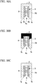
FIG. 11D is a cross-sectional view showing a clamping member. - Hereinafter, embodiments of the present invention will be described in detail with reference to the accompanying drawings.
- Here, in the following description, for clarification of respective components, some components are occasionally illustrated in different scale size in the drawings.
- With reference to
FIGS. 1 and 2 , aheat dissipating structure 1 according to an embodiment of the present invention will be described. - As shown in
FIGS. 1 and 2 , theheat dissipating structure 1 is a structure of a semiconductor device including aheat sink 2, a plurality of semiconductor modules (first heat generating components) 3, acircuit board 4, and a plurality of electronic components (second heat generating components) 5, wherein heat generated by thesemiconductor modules 3 and theelectronic components 5 is dissipated via theheat sink 2. - Specifically, in this
heat dissipating structure 1, theheat sink 2 is made of, for example, a material having a high thermal conductivity, such as Cu and Al. Theheat sink 2 has abase portion 6 and a plurality ofheat dissipating fins base portion 6 is formed in a rectangular plate shape. Each of theheat dissipating fins first surface 6a of thebase portion 6. Additionally, the plurality ofheat dissipating fins FIG. 2 ), of thebase portion 6. The plurality ofheat dissipating fins heat dissipating fins FIG. 2 ), of thebase portion 6. - In the present embodiment, the plurality of
heat dissipating fins base portion 6 such that the twoheat dissipating fins 7A are positioned along the both ends, in the long side direction, of thebase portion 6, and the twoheat dissipating fins 7B are positioned between the two heat-dissipatingfins 7A. Additionally, theheat dissipating fins 7B have larger dimensions in the height and thickness directions than theheat dissipating fins 7A, since asemiconductor module 3 is disposed into theheat dissipating fin 7B. Here, theheat sink 2 is not necessarily limited to those of this embodiment, and can be implemented by appropriately modifying the number, size, or the like of the respectiveheat dissipating fins - The
heat dissipating fin 7B is provided with aninsertion groove 8. Theinsertion groove 8 holds thesemiconductor module 3 that is insertable from aninsertion opening 8a provided on an end side of theheat dissipating fin 7B. Specifically, theinsertion groove 8 is a notch extending perpendicularly to thefirst surface 6a from the end side of theheat dissipating fin 7B, having a constant width, and having a depth enough to insert thesemiconductor module 3 therein. Theheat dissipating fin 7B is divided by theinsertion groove 8 into twofin portions - Additionally, the
heat dissipating fin 7B is provided with alid member 9a (not shown inFIG. 2 ) that closes theinsertion opening 8a. Thelid member 9a is mounted so as to close theinsertion opening 8a in a state where thesemiconductor module 3 is inserted into theinsertion groove 8. Here, the mounting structure of thelid member 9a is not necessarily limited to this structure, and may be a structure such that thelid member 9b (clamping member) is mounted so as to sandwich theheat dissipating fin 7B from the width direction of theinsertion groove 8, as shown in later-describedFIG. 11A to 11D . Additionally, thelid member 9a may be omitted. - As shown enlarged in
FIG. 3 , thesemiconductor module 3 includes afirst substrate 10, afirst semiconductor element 11, aconnector 12, asecond semiconductor element 13, and asecond substrate 14, which are layered in this order. - Among these, the first and
second substrates ceramic plates first substrate 10 and thesecond substrate 14 formrespective circuit pattern semiconductor module 3. Here, the first andsecond substrates - The first and
second semiconductor devices first semiconductor element 11 and thesecond semiconductor element 13 are mounted respectively on the opposing surface sides of thefirst substrate 10 and thesecond substrate 14, thus being electrically connected to therespective circuit patterns - The
connector 12 is made of a conductive material, such as Cu. Theconnector 12 has a first connectingportion 12a, a second connectingportion 12b, and a bridgingportion 12c. Among these, the first connectingportion 12a is a portion electrically connecting thefirst semiconductor element 11 and thesecond semiconductor element 13. The second connectingportion 12b is a portion to be electrically connected to one of thecircuit patterns 17a. The bridgingportion 12c is a portion connecting the first connectingportion 12a and the second connectingportion 12b. - The first connecting
portion 12a is formed in a columnar shape with a thickness sufficient to keep a distance between thefirst substrate 10 and thesecond substrate 14. Both end portions of the first connectingportion 12a are joined to thefirst semiconductor element 11 and thesecond semiconductor element 13 through a conductive adhesive (not shown), such as solder. The second connectingportion 12b is formed in a plate shape, and is joined to the one of thecircuit patterns 17a through a conductive adhesive (not shown), such as solder. The bridgingportion 12c is formed in an elongated plate shape with a length enough to connect the first connectingportion 12a and the second connectingportion 12b. One end side of the bridgingportion 12c is integrally connected to a side surface of the first connectingportion 12a. The other end side of the bridgingportion 12c is bent to the second connectingportion 12b side, thus being integrally connected to the second connectingportion 12b. - A
spacer 19 is disposed between thefirst substrate 10 and thesecond substrate 14. Thespacer 19, along with the first connectingportion 12a, keeps the distance between thefirst substrate 10 and thesecond substrate 14. Additionally, thespacer 19, as a circuit component of thesemiconductor module 3, is disposed in a state of being sandwiched between thecircuit patterns - The
circuit board 4 and the plurality ofelectronic components 5 shown inFIGS. 1 and 2 constitute acontroller 30 that controls driving of thesemiconductor module 3. Among these, thecircuit board 4 is bonded onto thesecond surface 6b, opposite to thefirst surface 6a, of the heat sink 2 (base portion 6). On the other hand, the plurality ofelectronic components 5 are mounted on thecircuit board 4. Eachelectronic component 5 is a heat generating component that generates a smaller amount of heat than eachsemiconductor module 3. - Some
electronic components 5 of the plurality ofelectronic components 5 and thesemiconductor modules 3 are electrically connected via aconnector 20. Theconnector 20 hasfirst outlets terminals semiconductor module 3 side are inserted, and asecond outlet 24 into which a second connectingterminal 23 on theelectronic component 5 side is inserted. The first connectingterminals semiconductor module 3 side, although not shown inFIG. 3 , are connected respectively to thecircuit patterns - The
heat sink 2 is provided with aninsertion hole 25 which insertably holds theconnector 20. Theheat sink 2 is provided with first through-holes terminals semiconductor module 3 side are penetrable. The first through-holes insertion groove 8 toward theinsertion hole 25. Theheat sink 2 and thecircuit board 4 are provided with a second through-hole 27 through which the second connectingterminal 23 on theelectronic component 5 side is penetrable. The second through-hole 27 is formed from the surface of thecircuit board 4 mounted with theelectronic components 5, toward theinsertion hole 25. Additionally, the first connectingterminals terminal 23 are electrically insulated from the first through-holes hole 27. - In the
heat dissipating structure 1 having the above structure, thesemiconductor modules 3, in the state of being inserted into theinsertion grooves 8, are in contact with the respective heat-dissipatingfins 7B. Thereby, heat emitted by thesemiconductor module 3 transmits from the inner wall surfaces of theinsertion groove 8, that are, from the first andsecond substrates fin portions heat dissipating fins 7B, thus being dissipated to the outside. On the other hand, heat emitted by the plurality ofelectronic components 5 transmits from thecircuit board 4 through thebase portion 6 to theheat dissipating fins semiconductor module 3 directly transmits to the heat-dissipatingfins 7B without through thebase portion 6, thus shortening the heat transfer path, thereby increasing the heat dissipation performance of thesemiconductor module 3. - As described above, in the
heat dissipating structure 1 of the present embodiment, thesemiconductor modules 3 are disposed in contact with theheat dissipating fins 7B, thereby making it possible to achieve high heat dissipation performance compared to conventional cases where thesemiconductor modules 3 are disposed on thesecond surface 6b of thebase portion 6. - Additionally, in the
heat dissipating structure 1 of the present embodiment, thesemiconductor modules 3 are disposed in the state of being inserted in theinsertion grooves 8, thus enabling miniaturization compared to the conventional cases where thesemiconductor modules 3 are disposed on thesecond surface 6b of thebase portion 6. Further, the first andsecond substrates semiconductor module 3 are made in contact with thefin portions semiconductor modules 3. - Moreover, in the
heat dissipating structure 1 of the present embodiment, thefirst semiconductor modules 3 disposed on thefirst surface 6a side of thebase portion 6 are electrically connected via theconnectors 20 to theelectronic components 5 disposed on thesecond surface 6b side of thebase portion 6. Thus, it is possible to connect thesemiconductor modules 3 and theelectronic components 5 by a short distance, thus making it possible to reduce the electrical resistance and to reduce the power loss. - Incidentally, regarding the
semiconductor module 3, as schematically shown inFIG. 4A , in order for ensuring of the insulation and protection against particles, amold resin 28 is provided to seal the opposing surface sides of thefirst substrate 10 and thesecond substrate 14. However, such amold resin 28 is likely to cause cracking and the like during thermal expansion, due to a large difference in linear expansion coefficient between the first andsecond semiconductor elements second substrates - In contrast, in the present invention, as schematically shown in
FIG. 4B , a configuration may be such that in place of themold resin 28, an insulatingfilm 29 is provided to cover the opposing surfaces of thefirst substrate 10 and thesecond substrate 14. As the insulatingfilm 29, an insulating material with high thermal conductivity, such as ceramic, is used. - In the
heat dissipating structure 1 of the present embodiment, thesemiconductor module 3 provided with such an insulatingfilm 29 is inserted into theinsertion groove 8, thereby making it possible to achieve securing of the insulation and protection against the particles. Additionally, in a case where the insulatingfilm 29 is provided, not only the heat dissipation performance from thesemiconductor modules 3 is enhanced by thinning the insulatingfilm 29, but also it becomes possible to suppress generation of cracks due to the difference in linear expansion coefficient. Further, since a step for sealing with themolding resin 28 can be omitted, thereby enabling simplification of the manufacturing process. - Here, the present invention is not necessarily limited to the above embodiment, and various modifications may be added without departing from the scope of the present invention.
- In the present invention, for example, it is also possible to change the connecting structure of the above-described
connector 20 that connects thesemiconductor module 3 and theelectronic component 5. Hereinafter, modified examples of theconnector 20 will be described. -
FIGS. 5A and 5B are views illustrating first modified examples of the connecting structure of theconnector 20 according to the present embodiment. A connecting structure of aconnector 31 according to the present first modified example has a configuration provided with, in place of the above-describedinsertion hole 25, aninsertion groove 32 which holds theconnector 31 that is insertable from thesecond surface 6b side of thebase portion 6. Additionally, a through-hole 33 is provided between a bottom surface of theinsertion groove 32 and the bottom surface of theinsertion groove 8. A hole dimension (horizontal width) of the through-hole 33 is smaller than a groove dimension (horizontal width) of theinsertion groove 32. Theconnector 31 has afirst outlet 35 into which a first connectingterminal 34 on thesemiconductor module 3 side is insertable, a plurality of second outlets 37 into which a plurality of second connectingterminals 36 on theelectronic component 5 side are insertable, and a protrudingportion 38 to fit into the through-hole 33. Thecircuit board 4 is provided with a through-hole 39 through which the plurality of second connectingterminals 36 are penetrable. - On the other hand, a connecting structure of a
connector 40 shown inFIG. 5B has a configuration provided with, in place of theinsertion hole 25, aninsertion groove 41 that holds theconnector 40 and thesemiconductor module 3 that are insertable from thefirst surface 6a side of thebase portion 6. Additionally, theinsertion groove 41 is provided with a through-hole 42. A hole dimension (horizontal width) of the through-hole 42 is smaller than a groove dimension (horizontal width) of theinsertion groove 41. Theconnector 40 has afirst outlet 44 into which a first connectingterminal 43 on thesemiconductor module 3 side is insertable, asecond outlet 46 into which a second connectingterminal 45 on theelectronic component 5 side is insertable, and a protrudingportion 47 to fit into the through-hole 42. - As described above, it is also possible to employ, in the first modified example of the present embodiment, the connecting structure of the
connector 31 shown inFIG 5A , or the connecting structure of theconnector 40 shown inFIG. 5B . -
FIGS. 6A and 6B are views illustrating a second modified example of the connecting structure of theconnector 20 according to the present embodiment. In the present second modified example, aheat sink 51 previously provided with a plurality ofconnectors 50 is used. Each of the plurality ofconnectors 50 has afirst outlet 52 on thefirst surface 6a of thebase portion 6 and asecond outlet 53 on thesecond surface 6b of thebase 6, so that the connecting terminal of thesemiconductor module 3 inserted between theheat dissipating fins 7 is insertable into thefirst outlet 52, and the connecting terminal of theelectronic component 5 is insertable into thesecond outlet 53. Here, arrangement, the number, and the like of the plurality ofconnectors 50 can be changed arbitrarily. -
FIGS. 7A to 7C are views illustrating a third modified example of the connecting structure of theconnector 20 according to the present embodiment. A connecting structure (heat sink 60) of aconnector 61 according to the present third modified example has a configuration that theconnector 61 is slidably mounted on theheat sink 60. Here, for clarification of the configuration of theconnector 61 itself, illustration of thesemiconductor modules 3, thecircuit board 4, and theelectronic components 5 is omitted inFIGS. 7B and7C . Additionally, although only oneconnector 61 is shown inFIGS. 7B and7C , the number ofconnectors 61 can be changed arbitrarily. - The connecting structure of the connector 61 (heat sink 60) has a configuration provided with, in place of the
insertion hole 25,slide grooves connector 61 that is insertable from thesecond surface 6b side of thebase portion 6 of theheat sink 60. The slide groove (first slide groove) 62 extends from thesecond surface 6b toward thefirst surface 6a of thebase portion 6 of theheat sink 60. The slide groove (second slide groove) 63 extends from thefirst surface 6a toward thesecond surface 6b of thebase portion 6 of theheat sink 60, and connects theslide groove 62 and theinsertion groove 8. In other words, theslide grooves base portion 6 in a direction from thefirst surface 6a toward thesecond surface 6b (vertical direction). A groove dimension (horizontal width) of theslide groove 63 is smaller than a groove dimension (horizontal width) of theslide groove 62. For this reason, even when theconnector 61 is inserted into theslide grooves second surface 6b side of thebase portion 6 of theheat sink 60, theconnector 61 does not fall from theslide grooves - The
slide grooves base portion 6 of theheat sink 60, between theadjacent fin portions fin portions first surface 6a of the base portion 6 (i.e., parallel to the insertion groove 8). Both end portions (i.e., both side surfaces), in the extending direction, of theslide grooves first surface 6a (or thesecond surface 6b) of thebase portion 6 of theheat sink 60 in plan view, as shown inFIG. 7C . In other words, theslide grooves base portion 6 in the direction from thefirst surface 6a toward thesecond surface 6b of the base portion 6 (vertical direction), but do not penetrate through thebase portion 6 in a direction parallel to the first andsecond surfaces connector 61 is slidable in theslide grooves slide grooves - The
connector 61 has afirst outlet 65 into/from which a first connectingterminal 64 of thesemiconductor module 3 is attachable/detachable, a plurality of second outlets 67 into/from which a plurality of second connectingterminals 66 of theelectronic component 5 are attachable/detachable, and a protrudingportion 68 to fit into the through-hole 63. Thefirst outlet 65 extends from a surface (third surface) of the two opposing surfaces of theconnector 61 which is on thefirst surface 6a side of thebase portion 6 toward the other surface (fourth surface) on thesecond surface 6b side of thebase portion 6. Additionally, the plurality of second outlets 67 extend from the surface (fourth surface) of the two opposing surfaces of theconnector 61 which is on thesecond surface 6b side of thebase portion 6 toward the other surface (third surface) on thefirst surface 6a side of thebase portion 6. - As shown in
FIG. 7B , the plurality of second outlets 67 includes a set of threesecond outlets 67a (first set) aligned parallel to the sliding direction of the connector 61 (extending direction of the slide groove), and a set of threesecond outlets 67b (second set) aligned vertical to the sliding direction of the connector 61 (extending direction of the slide groove). The first andsecond sets terminals 66 of theelectronic component 5 become attachable/detachable into/from any of the two sets ofsecond outlets - Additionally, the
circuit board 4 is provided with a through-slide-hole 69 through which the plurality of second connectingterminals 66 are penetrable. A position of the through-slide-hole 69 provided in thecircuit board 4 overlaps positions of theslide grooves connector 61 in plan view. Additionally, the plurality of second outlets 67 of theconnector 61 are positioned inside the through-slide-hole 69 in plan view. - According to this configuration, it becomes possible to slide the
connector 61 along theslide groove 62, thereby making it possible to more freely determine the position of theelectronic component 5 to be mounted on thecircuit board 4, compared to the configuration in which the position of the connector is fixed. Additionally, the plurality of second connectingterminals 66 of theelectronic component 5 becomes attachable/detachable into/from any one of the sets of thesecond outlets electronic component 5 when theelectronic component 5 is mounted on thecircuit board 4. -
FIGS. 8A to 8C are views illustrating a fourth modified example of the connecting structure of theconnector 20 according to the present embodiment. A connecting structure (heat sink 70) of aconnector 71 according to the present fourth modified example has a configuration that a plurality ofsecond outlets 77 are provided in a grid in plan view so that a plurality of second connectingterminals 76 of theelectronic component 5 are attachable/detachable thereinto/therefrom. Here, for clarification of the configuration of theconnector 71 itself, illustration of thesemiconductor modules 3, thecircuit board 4, and theelectronic components 5 is omitted inFIGS. 8B and 8C . Additionally, although only twoconnectors 71 are shown inFIGS. 8B and 8C , the number ofconnectors 71 may be changed arbitrarily. - The connecting structure (heat sink 70) of the
connector 71 has a configuration provided with, in place of the above-describedinsertion hole 25,insertion grooves connector 71 that is insertable from thesecond surface 6b side of thebase portion 6. Theinsertion groove 72 extends from thesecond surface 6b toward thefirst surface 6a of thebase portion 6 of theheat sink 70. Theinsertion groove 73 extends from thefirst surface 6a toward thesecond surface 6b of thebase portion 6 of theheat sink 70, and connects theinsertion groove 72 and theinsertion groove 8. In other words, theinsertion grooves base portion 6 in a direction from thefirst surface 6a toward thesecond surface 6b (vertical direction). A groove dimension (horizontal width) of theinsertion groove 73 is smaller than a groove dimension (horizontal width) of theinsertion groove 72. For this reason, even when theconnector 71 is inserted into theinsertion grooves second surface 6b side of thebase portion 6 of theheat sink 70, theconnector 71 does not fall from theinsertion grooves - The
insertion grooves base portion 6 of theheat sink 70, between theadjacent fin portions fin portions first surface 6a of the base portion 6 (i.e., parallel to the insertion groove 8). Both end portions (i.e., both side surfaces), in the extending direction, of theinsertion grooves first surface 6a (or thesecond surface 6b) of thebase portion 6 of theheat sink 70 in plan view, as shown inFIG. 8C . In other words, theinsertion grooves base portion 6 in the direction from thefirst surface 6a toward thesecond surface 6b of the base portion 6 (vertical direction), but do not penetrate through thebase portion 6 in a direction parallel to the first andsecond surfaces connector 61 is inserted into theinsertion grooves insertion grooves - The
connector 71 inserted into theinsertion grooves base portion 6 of theheat sink 70, between theadjacent fin portions fin portions first surface 6a of the base portion 6 (i. e., parallel to the insertion groove 8). Both end portions (i. e., both side surfaces), in the extending direction, of theconnector 71 are positioned inside thefirst surface 6a (or thesecond surface 6b) of thebase portion 6 of theheat sink 70 in plan view, as shown inFIG. 8C . - The
connector 71 has a plurality offirst outlets 75 into/from which a first connecting terminal 74 of thesemiconductor module 3 is attachable/detachable, a plurality ofsecond outlets 77 into/from which a plurality of second connectingterminals 76 of theelectronic component 5 are attachable/detachable, and a protrudingportion 78 to fit into the through-hole 73. The plurality offirst outlets 75 extend from a surface (third surface) of the two opposing surfaces of theconnector 71 which is on thefirst surface 6a side of thebase portion 6 toward the other surface (fourth surface) on thesecond surface 6b side of thebase portion 6. Additionally, the plurality ofsecond outlets 77 extend from a surface (fourth surface) of the two opposing surfaces of theconnector 71 which is on thesecond surface 6b side of thebase portion 6 toward the other surface (third surface) on thefirst surface 6a side of thebase portion 6. - As shown in
FIG. 8C , the plurality offirst outlets 75 are aligned in a line parallel to the extending direction of theinsertion grooves connector 71 which is on thefirst surface 6a side of thebase portion 6, in plan view. For this reason, the first connecting terminal 74 of thesemiconductor module 3 becomes attachable/detachable into/from any of the plurality offirst outlets 75. - Additionally, as shown in
FIG. 8B , the plurality ofsecond outlets 77 arranged in a grid on the surface (fourth surface) of the two opposing surfaces of theconnector 71, which is on thesecond surface 6b side of thebase portion 6, in plan view. The plurality ofsecond outlets 77 include a set of threesecond outlets 77a (first set) aligned vertical to the extending direction of the connector 71 (extending direction of theinsertion grooves second outlets 77b (second set) aligned parallel to the extending direction of the connector 71 (extending direction of theinsertion grooves terminals 76 of theelectronic component 5 become attachable/detachable into/from any of the plurality of first and second sets ofsecond outlets - The
circuit board 4 is provided with a through-slide-hole 79 through which the plurality of second connectingterminals 76 are penetrable. A position of the through-slide-hole 79 provided in thecircuit board 4 overlaps positions of theslide grooves connector 71 in plan view. Additionally, the plurality ofsecond outlets 77 of theconnector 71 are positioned inside the through-slide-hole 79 in plan view. - This configuration makes it possible to freely select an outlet into which the first connecting terminal 74 of the
semiconductor module 3 is to be inserted, from the plurality offirst outlets 75 aligned in a line on the surface (third surface) on thesemiconductor module 3 side of theconnector 71. For example, it becomes possible to arrange twosemiconductor modules 3 so as to be shifted away from each other through theheat dissipating fin 7, as shown in later-describedFIG. 9C . - Similarly, it becomes possible to freely select an outlet into which the plurality of second connecting
terminals 76 of theelectronic component 5 are to be inserted, from the plurality ofsecond outlets 77 arranged in a grid on the surface (fourth surface) on theelectronic component 5 side of theconnector 71. For example, it becomes possible to connect the three second connectingterminals 76 of theelectronic component 5 into the set of threesecond outlets 77b so that the long side of theelectronic component 5 becomes parallel to the long side of theconnector 71. Similarly, it becomes possible to connect the three second connectingterminals 76 of theelectronic component 5 into the set of threesecond outlets 77a so that the short side of theelectronic component 5 becomes parallel to the long side of theconnector 71. Thus, it becomes possible to freely determine disposition of thesemiconductor module 3 and theelectronic component 5 which are to be electrically connected by theconnector 71. - Additionally, a configuration may be such that the
semiconductor module 3 is in contact with at least oneheat dissipating fin 7A (7B) of the plurality ofheat dissipating fins semiconductor module 3 is sandwiched between the adjacentheat dissipating fins 7, as shown inFIG. 9A , or thesemiconductor module 3 is in contact with one side surface of theheat dissipating fin 7, as shown inFIG. 9B . Further, a configuration of thesemiconductor modules 3 is not limited to the above-described configuration that thesemiconductor modules 3 are disposed facing each other through theheat dissipating fin 7. Instead, a configuration may be such that thesemiconductor modules 3 are shifted away from each other through theheat dissipating fin 7, as shown inFIG 9C . - Further, the first heat generating components of the present invention are not necessarily limited to the above-described
semiconductor modules 3, and the arrangement, the number, and the like thereof can be modified appropriately. Additionally, theinsertion groove 8 can be modified appropriately in accordance with the size of the first heat generating components. Accordingly, the plurality ofheat dissipating fins 7 may be provided withinsertion grooves 8 with different depths and widths in accordance with the size of the respective first heat generating components. - Moreover, the present invention is not limited to the configuration provided with the
lid member 9a that closes the insertion opening of the above-describedinsertion groove 8. It is possible to employ a configuration provided with an insertion hole which insertably holds thesemiconductor module 3, such as the above-describedinsertion hole 25. - Additionally, in the present invention, for example, as shown in
FIG. 10A , in order to facilitate insertion of thesemiconductor module 3 into theinsertion groove 8, a configuration may be such that theinsertion opening 8a is provided with a taperedportion 8b. Further, theinsertion groove 8 is not limited to the above-described shape with a constant width. Instead, for example, a structure in a shape with a width gradually narrowed toward the end portion in the depth direction (so-called a wedge shape), as shown inFIG. 10B , or a structure in a shape with a width gradually narrowed toward the central portion in the depth direction (so-called an hourglass shape), as shown inFIG. 10C , may be employed in order to prevent thesemiconductor module 3 inserted into theinsertion groove 8 from being easily detached therefrom. Moreover, thesemiconductor modules 3 are inflated during heat dissipation and thus adheres tightly onto thefin portions - Additionally, in the present invention, the end portion of the
heat dissipating fin 7B may be provided with a clampingmember 9b shown inFIG. 11A , in place of thelid member 9a shown inFIG. 1 . The clampingmember 9b includes alid member 9b1 that covers theinsertion opening 8a, and a pair of clampingportions 9b2 provided upright from the both end portions, in a width direction (horizontal direction inFIG. 1 ), of thelid member 9b1. The clampingmember 9b is attached onto the end portion of theheat dissipating fin 7B such that while thesemiconductor module 3 is inserted into theinsertion groove 8, thelid member 9b1 covers theinsertion opening 8a, and the pair of clampingportions 9b2 sandwich thefin portions insertion groove 8. This makes it possible to increase the adhesion of thesemiconductor module 3 sandwiched between the pair offin portions fin portions semiconductor module 3 inserted into theinsertion groove 8 from falling therefrom. - Further, it is preferable that the clamping
member 9b is made of a material with a smaller linear expansion coefficient than that of theheat dissipating fin 7B (heat sink 2). In this case, the clampingmember 9b can prevent thefin portions heat dissipating fin 7B is thermally expanded by heat emitted from thesemiconductor module 3. This makes it possible to further increase the adhesion between thesemiconductor module 3 and theheat dissipating fin 7B (fin portions - Moreover, as shown in
FIGS. 11B to 11D , the clampingmember 9b shown inFIG. 11A may be applied to theheat dissipating fins 7B shown inFIGS. 10A to 10C . The structures shown inFIGS. 11B and11C are all provided with the clampingmember 9b that sandwiches theheat dissipating fin 7B from the width direction of theinsertion groove 8, thereby making it possible to increase the adhesion between thesemiconductor module 3 and theheat dissipating fin 7B (fin portions heat dissipating fin 7B is thermally expanded by heat emitted from thesemiconductor module 3, the clampingmember 9b prevents thefin portions semiconductor module 3 and theheat dissipating fin 7B (fin portions semiconductor module 3 toward theheat dissipating fin 7B even when an amount of heat emitted from thesemiconductor module 3 increases, thereby making it possible to achieve high dissipation performance. - The present invention is applicable to heat dissipating structures using heat sinks.
-
- 1 heat dissipating structure
- 2 heat sink
- 3 semiconductor module (first heat generating component)
- 4 circuit board
- 5 electronic component (second heat generating component)
- 6 base portion
- 6a first surface
- 6b second surface
- 7 heat dissipating fin
- 8 insertion groove
- 9a lid member
- 9b clamping member
- 10 first substrate
- 11 first semiconductor element
- 12 connector
- 13 second semiconductor element
- 14 second substrate
- 15, 16 ceramic plate (insulating plate)
- 17, 18 Cu layer (conductive layer)
- 17a, 18a circuit pattern
- 19 spacer
- 20 connector
- 21 a, 21 b first connecting terminal
- 22a, 22b first outlet
- 23 second connecting terminal
- 24 second outlet
- 25 insertion hole
- 26a, 26b first through-hole
- 27 second through-hole
- 28 mold resin
- 29 insulating film
- 30 controller
- 31 connector
- 32 insertion groove
- 33 through-hole
- 34 first connecting terminal
- 35 first outlet
- 36 second connecting terminal
- 37 second outlet
- 38 protruding portion
- 39 through-hole
- 40 connector
- 41 insertion groove
- 42 through-hole
- 43 first connecting terminal
- 44 first outlet
- 45 second connecting terminal
- 46 second outlet
- 47 protruding portion
- 50 connector
- 51 heat sink
- 52 first outlet
- 53 second outlet
- 60 heat sink
- 61 connector
- 62 slide groove
- 63 slide groove
- 64 first connecting terminal
- 65 first outlet
- 66 second connecting terminal
- 67 second outlet
- 68 protruding portion
- 69 through-slide-hole
- 70 heat sink
- 71 connector
- 72 insertion groove
- 73 insertion groove
- 74 first connecting terminal
- 75 first outlet
- 76 second connecting terminal
- 77 second outlet
- 78 protruding portion
- 79 through-slide-hole
Claims (11)
- A heat sink comprising:a base portion having a first surface and a second surface which oppose each other;at least one heat dissipating fin extending vertically from the first surface, each of the at least one heat dissipating fin having an insertion groove extending from an end portion thereof toward the base portion, and a first fin portion and a second fin portion which are separated by the insertion groove; anda connector included in the base portion, the connector being above the insertion groove in plan view, and the connector being configured to electrically connect a first heat generating component to be inserted into the insertion groove from a side of the first surface and a second heat generating component to be disposed on a side of the second surface.
- The heat sink according to claim 1, further comprising:a plurality of connectors including the connector, the plurality of connectors being included in the base portion, and the plurality of connectors being above the insertion groove in plan view.
- The heat sink according to claim 1, wherein the connector has:a third surface on the side of the first surface;a fourth surface on the side of the second surface, the fourth surface opposing the third surface;a first outlet extending from the third surface toward the fourth surface, a first connecting terminal of the first heat generating component being attachable and detachable into and from the first outlet; anda second outlet extending from the fourth surface toward the third surface, a second connecting terminal of the second heat generating component being attachable and detachable into and from the second outlet.
- The heat sink according to claim 3, wherein
the base portion has a slide groove extending parallel to the insertion groove, the base portion being above the insertion groove in plan view, and
the connector is slidable in the slide groove in parallel to the insertion groove. - The heat sink according to claim 4, wherein
the slide groove includes a first slide groove extending from the second surface toward the first surface, and a second slide groove extending from the first surface toward the second surface and connecting the first slide groove and the insertion groove,
both end portions, in an extending direction, of the first slide groove, and both end portions, in an extending direction, of the second slide groove are positioned inside the first surface or the second surface of the base portion in plan view, and
a groove dimension of the second slide groove is smaller than a groove dimension of the first slide groove. - The heat sink according to claim 4 or 5, wherein
the connector has a plurality of second outlets including the second outlet, the plurality of second outlets extending from the fourth surface toward the third surface,
the plurality of second outlets including a first set of three second outlets aligned parallel to an extending direction of the slide groove, and a second set of three second outlets aligned vertical to the extending direction of the slide groove,
the first set and the second set have a common center second outlet,
the second heat generating component has three second connecting terminals including the second connecting terminal, and
the three second connecting terminals are attachable and detachable into and from any of the first set and the second set. - The heat sink according to claim 1, wherein
the connector extends parallel to the insertion groove in plan view, and
the connector has:a plurality of first outlets including the first outlet, the plurality of first outlets being aligned parallel to the insertion groove on the third surface in plan view, anda plurality of second outlets including the second outlet, the plurality of second outlets being aligned in a grid on the fourth surface in plan view. - The heat sink according to claim 5, wherein
the first connecting terminal of the first heat generating component is attachable and detachable into and from any of the plurality of first outlets, and
the second connecting terminal of the second heat generating component is attachable and detachable into and from any of the plurality of second outlets. - The heat sink according to claim 7 or 8, wherein
the plurality of second outlets including a first set of three second outlets aligned parallel to an extending direction of the connector, and a second set of three second outlets aligned vertical to the extending direction of the connector,
the second heat generating component has three second connecting terminals including the second connecting terminal, and
the three second connecting terminals are attachable and detachable into and from any of the first set and the second set. - The heat sink according to claim 7, wherein both end portions, in an extending direction, of the connector are positioned inside the first surface or the second surface of the base portion in plan view.
- A heat dissipating structure comprising:a heat sink comprisinga base portion having a first surface and a second surface which oppose each other, andat least one heat dissipating fin extending vertically from the first surface, each of the at least one heat dissipating fin having an insertion groove extending from an end portion thereof toward the base portion, and a first fin portion and a second fin portion which are separated by the insertion groove;a first heat generating component to be inserted into the insertion groove from a side of the first surface;a circuit board on the second surface;a second heat generating component on the circuit board;a connector included in the base portion, the connector being above the insertion groove in plan view, and the connector being configured to electrically connect the first heat generating component and the second heat generating component.
Applications Claiming Priority (2)
| Application Number | Priority Date | Filing Date | Title |
|---|---|---|---|
| PCT/JP2014/078744 WO2016067383A1 (en) | 2014-10-29 | 2014-10-29 | Heat-dissipating structure |
| PCT/JP2015/061323 WO2016067659A1 (en) | 2014-10-29 | 2015-04-13 | Heat-dissipating structure |
Publications (2)
| Publication Number | Publication Date |
|---|---|
| EP3214647A1 true EP3214647A1 (en) | 2017-09-06 |
| EP3214647A4 EP3214647A4 (en) | 2018-05-30 |
Family
ID=55856770
Family Applications (1)
| Application Number | Title | Priority Date | Filing Date |
|---|---|---|---|
| EP15856013.6A Withdrawn EP3214647A4 (en) | 2014-10-29 | 2015-04-13 | Heat-dissipating structure |
Country Status (5)
| Country | Link |
|---|---|
| US (1) | US10159166B2 (en) |
| EP (1) | EP3214647A4 (en) |
| JP (1) | JP6021290B2 (en) |
| CN (1) | CN106575643B (en) |
| WO (2) | WO2016067383A1 (en) |
Cited By (1)
| Publication number | Priority date | Publication date | Assignee | Title |
|---|---|---|---|---|
| DE102021121797A1 (en) | 2021-08-23 | 2023-02-23 | Infineon Technologies Ag | POWER SEMICONDUCTOR MODULE WITH SOCKET OR PRESS-FIT PIN AND METHOD OF ITS MANUFACTURE |
Families Citing this family (14)
| Publication number | Priority date | Publication date | Assignee | Title |
|---|---|---|---|---|
| WO2016067377A1 (en) * | 2014-10-29 | 2016-05-06 | 新電元工業株式会社 | Heat-dissipating structure |
| US11476179B2 (en) * | 2016-10-25 | 2022-10-18 | Tesla, Inc. | Inverter |
| WO2018146815A1 (en) * | 2017-02-13 | 2018-08-16 | 新電元工業株式会社 | Electronic module |
| WO2018146816A1 (en) * | 2017-02-13 | 2018-08-16 | 新電元工業株式会社 | Electronic device |
| CN109314087B (en) * | 2017-05-19 | 2022-08-02 | 新电元工业株式会社 | Electronic module, method for manufacturing connection body, and method for manufacturing electronic module |
| JP7280678B2 (en) * | 2017-11-14 | 2023-05-24 | キヤノン株式会社 | Electronics |
| WO2019142253A1 (en) | 2018-01-17 | 2019-07-25 | 新電元工業株式会社 | Electronic module |
| CN112368829B (en) | 2018-07-04 | 2024-05-14 | 新电元工业株式会社 | Electronic module |
| JP7204174B2 (en) * | 2018-07-19 | 2023-01-16 | マイクロモジュールテクノロジー株式会社 | Semiconductor device and method for manufacturing semiconductor device |
| CN112259513B (en) * | 2020-10-22 | 2023-09-26 | 湖南国芯半导体科技有限公司 | A double-sided heat dissipation power module and its packaging method |
| WO2022163658A1 (en) * | 2021-01-27 | 2022-08-04 | 京セラ株式会社 | Heater element positioning substrate, heating module, and heating device |
| US11520391B1 (en) * | 2021-05-14 | 2022-12-06 | AA Power Inc. | Power supply for a mining machine |
| CN114828518B (en) * | 2022-04-25 | 2022-11-18 | 广东合通建业科技股份有限公司 | Multifunctional PCB (printed circuit board) |
| CN120978429B (en) * | 2025-10-17 | 2025-12-30 | 中国科学技术大学 | Electrical connectors, signal transmission devices, and dilution refrigeration units |
Family Cites Families (25)
| Publication number | Priority date | Publication date | Assignee | Title |
|---|---|---|---|---|
| JPS57202763A (en) * | 1981-06-09 | 1982-12-11 | Fujitsu Ltd | Electronic device |
| JPS58158448U (en) * | 1981-10-19 | 1983-10-22 | 日本電信電話株式会社 | semiconductor heat dissipation device |
| JPS58158448A (en) | 1982-03-17 | 1983-09-20 | Matsushita Electric Ind Co Ltd | heat pump water heater |
| JPH04188861A (en) * | 1990-11-22 | 1992-07-07 | Nippon Telegr & Teleph Corp <Ntt> | Electronic circuit package |
| JPH089433B2 (en) | 1991-09-06 | 1996-01-31 | ジューキ株式会社 | Encapsulation equipment |
| JP2570832Y2 (en) * | 1992-02-28 | 1998-05-13 | 日本電気株式会社 | Heat sink for semiconductor |
| JP3159071B2 (en) * | 1996-08-01 | 2001-04-23 | 株式会社日立製作所 | Electric device having radiating fins |
| JP3470041B2 (en) * | 1998-04-28 | 2003-11-25 | 京セラ株式会社 | Hybrid integrated circuit device |
| JP3565152B2 (en) * | 2000-09-26 | 2004-09-15 | 株式会社ノーリツ | Heat dissipation member |
| JP2002359329A (en) * | 2001-05-30 | 2002-12-13 | Hitachi Ltd | Semiconductor device |
| JP3935381B2 (en) * | 2002-03-14 | 2007-06-20 | 松下電器産業株式会社 | Electronic circuit device having double-sided electrode semiconductor element and method of manufacturing the electronic circuit device |
| JP4360404B2 (en) * | 2004-03-18 | 2009-11-11 | 三菱電機株式会社 | Control device using module heat dissipation structure |
| JP4979909B2 (en) * | 2005-08-19 | 2012-07-18 | 株式会社日立製作所 | Power converter |
| JP2008282931A (en) * | 2007-05-09 | 2008-11-20 | Fujitsu Ten Ltd | Electrical circuit device |
| JP2010187504A (en) * | 2009-02-13 | 2010-08-26 | Mitsubishi Electric Corp | Inverter device |
| DE102009044368B4 (en) * | 2009-10-30 | 2014-07-03 | Lear Corporation Gmbh | cooling arrangement |
| JP2011103395A (en) * | 2009-11-11 | 2011-05-26 | Sumitomo Electric Ind Ltd | Heat radiating structure of heat generating component and circuit device including the same heat radiating structure |
| JP2011114176A (en) * | 2009-11-27 | 2011-06-09 | Mitsubishi Electric Corp | Power semiconductor device |
| JP5965912B2 (en) * | 2011-10-13 | 2016-08-10 | 株式会社日立製作所 | Power semiconductor module, power conversion device and electric vehicle |
| JP5484429B2 (en) | 2011-11-18 | 2014-05-07 | 三菱電機株式会社 | Power converter |
| US9474189B2 (en) * | 2012-05-23 | 2016-10-18 | Mitsubishi Electric Corporation | Inverter device |
| JP2014154391A (en) * | 2013-02-08 | 2014-08-25 | Denso Corp | Light emitting device |
| WO2014132425A1 (en) * | 2013-02-28 | 2014-09-04 | 新電元工業株式会社 | Electronic module and production method for same |
| CN104303289B (en) * | 2013-05-13 | 2017-10-24 | 新电元工业株式会社 | Electronic module and its manufacture method |
| WO2015152667A1 (en) * | 2014-04-04 | 2015-10-08 | 엘지이노텍 주식회사 | Lighting module and lighting apparatus including same |
-
2014
- 2014-10-29 WO PCT/JP2014/078744 patent/WO2016067383A1/en not_active Ceased
-
2015
- 2015-04-13 JP JP2015558054A patent/JP6021290B2/en active Active
- 2015-04-13 CN CN201580044053.6A patent/CN106575643B/en active Active
- 2015-04-13 WO PCT/JP2015/061323 patent/WO2016067659A1/en not_active Ceased
- 2015-04-13 EP EP15856013.6A patent/EP3214647A4/en not_active Withdrawn
- 2015-04-13 US US15/520,604 patent/US10159166B2/en active Active
Cited By (2)
| Publication number | Priority date | Publication date | Assignee | Title |
|---|---|---|---|---|
| DE102021121797A1 (en) | 2021-08-23 | 2023-02-23 | Infineon Technologies Ag | POWER SEMICONDUCTOR MODULE WITH SOCKET OR PRESS-FIT PIN AND METHOD OF ITS MANUFACTURE |
| US12469770B2 (en) | 2021-08-23 | 2025-11-11 | Infineon Technologies Ag | Power semiconductor module with rivet or press fit pin and method for fabricating the same |
Also Published As
| Publication number | Publication date |
|---|---|
| US10159166B2 (en) | 2018-12-18 |
| JP6021290B2 (en) | 2016-11-09 |
| JPWO2016067659A1 (en) | 2017-04-27 |
| CN106575643A (en) | 2017-04-19 |
| EP3214647A4 (en) | 2018-05-30 |
| WO2016067383A1 (en) | 2016-05-06 |
| CN106575643B (en) | 2018-10-16 |
| WO2016067659A1 (en) | 2016-05-06 |
| US20170311482A1 (en) | 2017-10-26 |
Similar Documents
| Publication | Publication Date | Title |
|---|---|---|
| US10159166B2 (en) | Heat dissipating structure | |
| US9860990B1 (en) | Circuit board structure with chips embedded therein and manufacturing method thereof | |
| CN110933900B (en) | Electrical Equipment and Radiators | |
| JP6809294B2 (en) | Power module | |
| KR100752239B1 (en) | Power module package structure | |
| US10251256B2 (en) | Heat dissipating structure | |
| CN104112720A (en) | Power semiconductor assembly and module | |
| JP7059714B2 (en) | Power converter and manufacturing method of power converter | |
| US11201101B2 (en) | Electronic component | |
| CN104137259B (en) | Electronic module and manufacture method thereof | |
| US7672140B2 (en) | Circuit board configuration | |
| JP2017005129A (en) | Semiconductor device | |
| JP6091035B2 (en) | Heat dissipation structure | |
| JP6488658B2 (en) | Electronic equipment | |
| CN102960079B (en) | Electronic equipment with a housing made of molded material | |
| KR20060105403A (en) | Package structure with hybrid circuit and composite board | |
| JP6336106B2 (en) | Heat dissipation structure | |
| JP2017011027A (en) | Circuit board heat dissipation structure | |
| JP2016152290A (en) | Thermal conductive substrate and method for mounting electronic component | |
| CN101145550A (en) | Semiconductor device and electronic circuit device using the semiconductor device | |
| CN108738367A (en) | Electronic module | |
| JP2017117903A (en) | Circuit structure | |
| JP2017034211A (en) | Heat radiator, electronic device, and manufacturing method for electronic device |
Legal Events
| Date | Code | Title | Description |
|---|---|---|---|
| STAA | Information on the status of an ep patent application or granted ep patent |
Free format text: STATUS: THE INTERNATIONAL PUBLICATION HAS BEEN MADE |
|
| PUAI | Public reference made under article 153(3) epc to a published international application that has entered the european phase |
Free format text: ORIGINAL CODE: 0009012 |
|
| STAA | Information on the status of an ep patent application or granted ep patent |
Free format text: STATUS: REQUEST FOR EXAMINATION WAS MADE |
|
| 17P | Request for examination filed |
Effective date: 20170213 |
|
| AK | Designated contracting states |
Kind code of ref document: A1 Designated state(s): AL AT BE BG CH CY CZ DE DK EE ES FI FR GB GR HR HU IE IS IT LI LT LU LV MC MK MT NL NO PL PT RO RS SE SI SK SM TR |
|
| AX | Request for extension of the european patent |
Extension state: BA ME |
|
| DAV | Request for validation of the european patent (deleted) | ||
| DAX | Request for extension of the european patent (deleted) | ||
| A4 | Supplementary search report drawn up and despatched |
Effective date: 20180503 |
|
| RIC1 | Information provided on ipc code assigned before grant |
Ipc: H01L 25/07 20060101ALI20180425BHEP Ipc: H01L 25/18 20060101ALI20180425BHEP Ipc: H01R 12/73 20110101ALI20180425BHEP Ipc: H01L 23/367 20060101ALI20180425BHEP Ipc: H01L 23/36 20060101AFI20180425BHEP Ipc: H05K 7/00 20060101ALI20180425BHEP Ipc: H05K 7/20 20060101ALI20180425BHEP |
|
| GRAP | Despatch of communication of intention to grant a patent |
Free format text: ORIGINAL CODE: EPIDOSNIGR1 |
|
| STAA | Information on the status of an ep patent application or granted ep patent |
Free format text: STATUS: GRANT OF PATENT IS INTENDED |
|
| INTG | Intention to grant announced |
Effective date: 20210723 |
|
| STAA | Information on the status of an ep patent application or granted ep patent |
Free format text: STATUS: THE APPLICATION IS DEEMED TO BE WITHDRAWN |
|
| 18D | Application deemed to be withdrawn |
Effective date: 20211203 |