EP3211968B1 - Système de commutation destiné au fonctionnement d'au moins une lampe à del - Google Patents
Système de commutation destiné au fonctionnement d'au moins une lampe à del Download PDFInfo
- Publication number
- EP3211968B1 EP3211968B1 EP16450029.0A EP16450029A EP3211968B1 EP 3211968 B1 EP3211968 B1 EP 3211968B1 EP 16450029 A EP16450029 A EP 16450029A EP 3211968 B1 EP3211968 B1 EP 3211968B1
- Authority
- EP
- European Patent Office
- Prior art keywords
- circuit arrangement
- terminals
- lines
- led
- led light
- Prior art date
- Legal status (The legal status is an assumption and is not a legal conclusion. Google has not performed a legal analysis and makes no representation as to the accuracy of the status listed.)
- Active
Links
Images


Classifications
-
- B—PERFORMING OPERATIONS; TRANSPORTING
- B31—MAKING ARTICLES OF PAPER, CARDBOARD OR MATERIAL WORKED IN A MANNER ANALOGOUS TO PAPER; WORKING PAPER, CARDBOARD OR MATERIAL WORKED IN A MANNER ANALOGOUS TO PAPER
- B31D—MAKING ARTICLES OF PAPER, CARDBOARD OR MATERIAL WORKED IN A MANNER ANALOGOUS TO PAPER, NOT PROVIDED FOR IN SUBCLASSES B31B OR B31C
- B31D5/00—Multiple-step processes for making three-dimensional [3D] articles
- B31D5/0086—Making hollow objects
-
- A—HUMAN NECESSITIES
- A63—SPORTS; GAMES; AMUSEMENTS
- A63H—TOYS, e.g. TOPS, DOLLS, HOOPS OR BUILDING BLOCKS
- A63H33/00—Other toys
- A63H33/16—Models made by folding paper
-
- F—MECHANICAL ENGINEERING; LIGHTING; HEATING; WEAPONS; BLASTING
- F21—LIGHTING
- F21V—FUNCTIONAL FEATURES OR DETAILS OF LIGHTING DEVICES OR SYSTEMS THEREOF; STRUCTURAL COMBINATIONS OF LIGHTING DEVICES WITH OTHER ARTICLES, NOT OTHERWISE PROVIDED FOR
- F21V25/00—Safety devices structurally associated with lighting devices
- F21V25/02—Safety devices structurally associated with lighting devices coming into action when lighting device is disturbed, dismounted, or broken
- F21V25/04—Safety devices structurally associated with lighting devices coming into action when lighting device is disturbed, dismounted, or broken breaking the electric circuit
-
- F—MECHANICAL ENGINEERING; LIGHTING; HEATING; WEAPONS; BLASTING
- F21—LIGHTING
- F21V—FUNCTIONAL FEATURES OR DETAILS OF LIGHTING DEVICES OR SYSTEMS THEREOF; STRUCTURAL COMBINATIONS OF LIGHTING DEVICES WITH OTHER ARTICLES, NOT OTHERWISE PROVIDED FOR
- F21V25/00—Safety devices structurally associated with lighting devices
- F21V25/10—Safety devices structurally associated with lighting devices coming into action when lighting device is overloaded, e.g. thermal switch
-
- H—ELECTRICITY
- H05—ELECTRIC TECHNIQUES NOT OTHERWISE PROVIDED FOR
- H05B—ELECTRIC HEATING; ELECTRIC LIGHT SOURCES NOT OTHERWISE PROVIDED FOR; CIRCUIT ARRANGEMENTS FOR ELECTRIC LIGHT SOURCES, IN GENERAL
- H05B45/00—Circuit arrangements for operating light-emitting diodes [LED]
-
- H—ELECTRICITY
- H05—ELECTRIC TECHNIQUES NOT OTHERWISE PROVIDED FOR
- H05B—ELECTRIC HEATING; ELECTRIC LIGHT SOURCES NOT OTHERWISE PROVIDED FOR; CIRCUIT ARRANGEMENTS FOR ELECTRIC LIGHT SOURCES, IN GENERAL
- H05B45/00—Circuit arrangements for operating light-emitting diodes [LED]
- H05B45/30—Driver circuits
- H05B45/357—Driver circuits specially adapted for retrofit LED light sources
-
- Y—GENERAL TAGGING OF NEW TECHNOLOGICAL DEVELOPMENTS; GENERAL TAGGING OF CROSS-SECTIONAL TECHNOLOGIES SPANNING OVER SEVERAL SECTIONS OF THE IPC; TECHNICAL SUBJECTS COVERED BY FORMER USPC CROSS-REFERENCE ART COLLECTIONS [XRACs] AND DIGESTS
- Y02—TECHNOLOGIES OR APPLICATIONS FOR MITIGATION OR ADAPTATION AGAINST CLIMATE CHANGE
- Y02B—CLIMATE CHANGE MITIGATION TECHNOLOGIES RELATED TO BUILDINGS, e.g. HOUSING, HOUSE APPLIANCES OR RELATED END-USER APPLICATIONS
- Y02B20/00—Energy efficient lighting technologies, e.g. halogen lamps or gas discharge lamps
- Y02B20/30—Semiconductor lamps, e.g. solid state lamps [SSL] light emitting diodes [LED] or organic LED [OLED]
Definitions
- the present invention relates to a circuit arrangement for operating at least one LED light with lines for connecting the LED light to an electrical supply network.
- LED lights are advantageous over fluorescent tubes because they do not require ballasts to start up and because they require significantly less electricity. This means that LED lights are much more cost-effective than fluorescent tubes to produce, install and operate.
- Fluorescent tubes are usually designed with contact pins at their two end faces, which can be used in contact sockets of fastening sockets which are located in a supply and control circuit. Since LED lights are often designed with contact pins in the same way, it is possible to use an LED light in a fitting for a fluorescent tube or to use a fluorescent tube in a fitting for an LED light. If a fluorescent tube is used in a fitting for an LED lamp, however, there is a risk of an implosion or explosion of the fluorescent tube with the risk of injury and the environmentally harmful fluorescent gases in the fluorescent tube escaping into the atmosphere.
- the reason for this is that there are heating coils in fluorescent tubes for igniting the electrical discharge, which have a very low ohmic resistance.
- the ballasts which are assigned to the fittings for fluorescent tubes, the current supplied to the heating coils located in the fluorescent tubes is controlled in the manner required for their operation. If, however, no ballasts are provided, since they are not required for LED lights, the current flowing through the heating coil increases so quickly when a fluorescent tube is fed that the fluorescent tube can explode as a result.
- the DE 102014204875 A1 , the WO 2011/014111 A1 , the DE 202010010536 U1 and the AU 2009101044 A4 disclose circuit arrangements for LED lights in which there are protective circuits against overcurrents. If fluorescent tubes are mistakenly used in these circuit arrangements, such overcurrents are prevented by the protective circuits. However, the effectiveness of these protective circuits is so slow that damage, in particular the triggering of downstream fuses, can be caused. If these protective circuits contain fuses, they are also disadvantageous because new fuses must be used as a result.
- the DE 19900889 A1 discloses a circuit arrangement for fluorescent lamps which is equipped with inductive ballasts which can be converted to fluorescent lamps in electronic operation and with improved efficiency. This is achieved by using additional adapters and by bridging the contacts of the start detection (10) via a PTC resistor.
- the WO 2015/014680 A1 and the WO 2015/014584 A1 disclose LED lights in which PTC resistors are built in to enable safe operation, even if they are connected to a ballast in the circuit arrangement.
- the present invention is based on the object of creating a circuit arrangement for at least one fitting for receiving an LED light, through which the operation of an LED light is guaranteed and through which, however, the power supply when a fluorescent tube is inserted into the fitting for feeding the fluorescent tube is controlled in such a way that it is limited in order to prevent the fluorescent tube from exploding.
- the circuit arrangement preferably has a carrier which is designed with first terminals for connection to the electrical supply network and with second terminals for connection of at least one LED light, the first and second terminals being connected to one another by means of electrical lines
- the PTC resistor is located in at least one of these lines.
- four second terminals are provided in the circuit arrangement, one phase conductor and the neutral conductor being connected to two second terminals via lines and the two further second terminals being connected to one another by means of a line in which the PTC resistor is located.
- the circuit arrangement is formed with two groups of second terminals, to which feed lines for two LED lights can be clamped, with at least one current-limiting component, namely a PTC resistor, being provided in the lines leading from the supply network in each of the two groups.
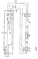
- the circuit arrangement 1 shown has connection terminals 11, 12 and 13 for a phase conductor L, a neutral conductor N and a protective conductor PE, with a current-limiting electrical component 2 in the form of a PTC resistor (Positive Temperature Coefficient resistor) and with a tubular LED light 3 trained.
- the LED lamp 3 are on a support plate, a housing or the like.
- the mounting base (G13 base) 4 and 5 are assigned.
- the LED lamp 3 is formed at its two front ends with contact pins 31, 31a and 32, 32a. Inside the LED lamp 3 there is a fuse 33, an AC / DC converter 34 and a large number of LED elements 35.
- the mounting bases 4 and 5 are connected to the contact pins 31, 31a, 32, 32a assigned contact sockets 41, 41a, 51, 51a formed in which the Contact pins 31, 31a, 32, 32a of the LED lamp 3 can be used, whereby it is fastened in the fitting and can be connected to the supply network.
- connection terminal 11 a line 11a leads to the contact socket 41 of the fastening base 4, from the connection terminal 12 a line 12a leads to the contact socket 51 of the fastening base 5 and from the connection terminal 13 a line 13a leads away, by means of which the carrier, the housing and the like . for the circuit arrangement 1 is grounded.
- a line 2a leads from the contact socket 41a to the contact socket 51a.
- the current-limiting electrical component 2 is located in this line 2a in the form of a PTC resistor (Positive Temperature Coefficient resistor). This is a resistor whose resistance value increases sharply with increasing temperature, with the resistance characteristic curve having a very steep profile from a nominal temperature.
- the LED light 3 is inserted into the mounting bases 4 and 5. As soon as the LED lamp 3 is connected to the supply network, it is fed via the circuit arrangement 1 with alternating current with a voltage of approximately 230 V or with a power of approximately 30 W.
- the fuse 33 located in the LED lamp 3, which is designed as a quick fuse (F), is used to limit the current supplied to the LED lamp 3 to about 0.5 A.
- the converter 34 located in the LED lamp 3 is used for Conversion of the alternating current supplied to the LED lamp 3 into a direct current of 0.7 A for feeding the series-connected LED elements 35.
- the current-limiting component 2 in the form of a PTC resistor is provided in the circuit arrangement 1, by means of which a sharp increase in the current supplied to the fluorescent tube is immediately prevented.
- the current-limiting component 2 is inserted into the line 2a.
- the current-limiting component 2 can, however, also be inserted into the line 11a or into the line 12a, as shown in dashed lines.
- a second such component can be used in the lines connected to the LED lamp 3 in the event that the first component 2 is inoperable. However, this redundancy causes a loss of performance.
- At least one current-limiting component 2 in the form of a PTC resistor is located in the lines connected to the LED light.
- FIG.2 Another circuit arrangement 1 a according to the invention is shown, which forms an additional device with a current-limiting electrical component 2 in a fitting for an LED lamp 3.
- connection terminals are provided, which are assigned to the four contact pins of the LED lights.
- this is on a carrier or the like.
- the circuit arrangement located which represents an additional device when installing an LED light, is also designed with four connecting terminals to which the feed lines for the LED light are clamped.
- the circuit arrangement 1 a is designed with connection terminals 11, 12 and 13 for a phase conductor L, a neutral conductor N and a protective conductor PE. From the connector 11 leads a line 11a to a connection terminal 14, from the terminal 12 a line 12a leads to a connection terminal 15 and from the connection terminal 13 a line 13a leads away, by means of which a carrier or a housing for the circuit arrangement 1a is grounded.
- two further connection terminals 16 and 17 are provided, to which a line 21 is connected, in which the current-limiting electrical component 2 is located in the form of a PTC resistor (Positive Temperature Coefficient resistor).
- a line 14a leads from the fastening terminal 14 to the contact socket 41 of the fastening base 4, from the connection terminal 15 a line 15a leads to the contact socket 51 of the fastening base 5, from the connection terminal 16 a line 16a leads to the contact socket 41a of the fastening base 4 and from the connection terminal 17 a line 17a to the contact socket 51a of the fastening base 5.
- the LED light 3 is inserted into the mounting bases 4 and 5. As soon as the LED lamp 3 is connected to the supply network, it is fed via the circuit arrangement 1 a with alternating current with a voltage of approximately 230 V or with a power of approximately 30 W.
- the fuse 33 located in the LED lamp 3, which is designed as a quick fuse (F), is used to limit the current supplied to the LED lamp 3 to about 0.5 A.
- the converter 34 located in the LED lamp 3 is used for Conversion of the alternating current supplied to the LED light 3 into a direct current of 0.7 A for supplying the series-connected LED elements 35.
- the current-limiting component 2 is provided in the circuit arrangement 1 a, by means of which a strong increase in the current supplied to the fluorescent tube is directly prevented.
- the current-limiting component 2 is inserted into the line 21.
- This component 2 can, however, also be inserted into the line 11a or into the line 12a, as shown in dashed lines.
- a second such component can be inserted into the feed line to the LED light 3 in the event that the first component 2 is inoperable.
- this redundancy causes a loss of performance.
- At least one current-limiting component 2 in the form of a PTC resistor is located in the feed line for an LED lamp.
- ballasts are required for LED lights, they can be connected to the supply network by means of the circuit arrangement 1 a, which is designed with four terminals, in accordance with the usual assembly method.
- a current-limiting component in the form of a PTC resistor is located in at least one of the lines leading to the four connection terminals, which prevents the fluorescent tube from exploding.
- FIG.3 a circuit arrangement 1b according to the invention is shown, to which fittings for two LED lights 3 and 3a can be connected.
- the circuit arrangement 1b is also designed with connection terminals 11, 12 and 13 for a phase conductor L, a neutral conductor N and a protective conductor PE.
- a line 11a leads from the terminal 11 to a first line group I with one Connection terminal 14, from the terminal 12 a line 12a leads to a terminal 15 and from the terminal 13 a line 13a leads away, by means of which a carrier or a housing for the circuit arrangement 1b is grounded.
- two further terminals 16 and 17 are provided, to which a line 21 is connected, in which there is a current-limiting electrical component 2 in the form of a PTC resistor (Positive Temperature Coefficient resistor).
- a first LED light 3 is connected to this first line group I via a first group of lines 14a, 15a, 16a and 17a.
- a second line group II parallel to the first line group I is also provided, which leads to a second group of connection terminals 14, 15, 16 and 17, to which a second group of lines 14a, 15a, 16a and 17a is used to connect first LED lamp 3 connected in parallel second LED lamp 3a is connected.
- the supply, the design and the mode of operation of the two LED lights 3 and 3a please refer to the explanations relating to the LED light 3 in FIG.2 Reference is made to the fact that this also applies to the FIG.3 are applicable.
- both of these line groups I and II there is at least one current-limiting resistor 2 in the form of a PTC resistor for protection in the event of fluorescent tubes being inserted in error.
- the circuit arrangement 1b serves as an additional device to which two LED lights 3 and 3a can be connected.
- a protective circuit 1a or 1b must be installed in its place in the event that a fluorescent tube is mistakenly used instead of an LED light. For the same reason, a protective circuit 1, 1a or 1b must be provided when installing a lighting system with LED lights when connecting to the supply network.
Landscapes
- Engineering & Computer Science (AREA)
- General Engineering & Computer Science (AREA)
- Circuit Arrangement For Electric Light Sources In General (AREA)
Claims (4)
- Agencement de circuit pour l'utilisation d'au moins une lampe à LED (3, 3a), l'agencement de circuit comportant au moins une lampe à LED (3, 3a), des socles de fixation (4, 5) comportant des douilles de contact (41,41a,51,51a) pour des broches de contact (31,31a,32,32a) de la lampe à LED (3, 3a), des câbles (2a, 11a, 12a, 14a, 15a, 16a, 17a, 21) connectés au douilles de contact (41,51) pour le raccordement des lampes à LED (3, 3a) à un réseau d'alimentation électrique et une pièce électrotechnique (2) dans un des câbles (2a, 21) pour la limitation du courant, caractérisé en ce que la pièce électrotechnique (2) est une résistance PTC (2).
- Agencement de circuit selon la revendication 1, caractérisé en ce qu'il est réalisé avec un support qui est réalisé avec de premières bornes (11,12,13) pour le raccordement à un réseau d'alimentation électrique et avec de secondes bornes (14,15,16,17) pour le raccordement de l'au moins une lampe à LED (3, 3a), les premières et les secondes bornes étant connectées entre elles au moyen d'autres câbles électriques (11a, 12a, 21) et que la résistance PTC (2)se trouve dans au moins un de ces autres câbles (11a, 12a, 21) .
- Agencement de circuit selon la revendication 1, caractérisé en ce qu'il présente deux lampes à LED (3, 3a) et est réalisé avec un support qui est réalisé avec de premières bornes (11,12,13) pour le raccordement à un réseau d'alimentation électrique et avec quatre secondes bornes (14,15,16,17) pour le raccordement de respectivement au moins une des lampes à LED (3, 3a), un conducteur de phase (11) et un conducteur neutre (12) étant connectables par d'autres câbles (11a, 12a) à deux autres bornes (14,15) et les deux autres secondes bornes (16,17) étant connectées entre elles au moyen d'un câble supplémentaire dans lequel se trouve la résistance PTC (2) .
- Agencement de circuit selon la revendication 3, caractérisé en ce qu'il est réalisé avec deux groupes (I, II) de secondes bornes (14,15,16,17) auxquelles des câbles d'alimentation (14a, 15a, 16a, 17a) pour les deux lampes à LED (3, 3a) peuvent être fixés, étant prévue, dans des câbles de raccordement (11a, 12a) partant du réseau d'alimentation pour chacun des deux groupes (I, II), au moins une pièce de limitation de courant (2), à savoir respectivement une résistance PTC (2).
Applications Claiming Priority (1)
| Application Number | Priority Date | Filing Date | Title |
|---|---|---|---|
| AT992016 | 2016-02-25 |
Publications (2)
| Publication Number | Publication Date |
|---|---|
| EP3211968A1 EP3211968A1 (fr) | 2017-08-30 |
| EP3211968B1 true EP3211968B1 (fr) | 2020-12-30 |
Family
ID=57286434
Family Applications (1)
| Application Number | Title | Priority Date | Filing Date |
|---|---|---|---|
| EP16450029.0A Active EP3211968B1 (fr) | 2016-02-25 | 2016-11-02 | Système de commutation destiné au fonctionnement d'au moins une lampe à del |
Country Status (2)
| Country | Link |
|---|---|
| EP (1) | EP3211968B1 (fr) |
| AT (1) | AT15590U1 (fr) |
Families Citing this family (1)
| Publication number | Priority date | Publication date | Assignee | Title |
|---|---|---|---|---|
| CN109915797B (zh) | 2017-12-11 | 2021-11-30 | 朗德万斯公司 | 用于led照明模组的电子驱动器以及led灯 |
Citations (1)
| Publication number | Priority date | Publication date | Assignee | Title |
|---|---|---|---|---|
| WO2015014584A1 (fr) * | 2013-07-30 | 2015-02-05 | Koninklijke Philips N.V. | Lampe de remplacement à led pour un fonctionnement dans des conditions de sécurité à ballast électromagnétique |
Family Cites Families (7)
| Publication number | Priority date | Publication date | Assignee | Title |
|---|---|---|---|---|
| DE19900889B4 (de) * | 1999-01-12 | 2004-04-15 | Suresh Hiralal Shah | Bausatz zum Umrüsten von Leuchten mit geraden, beidseitig gesockelten Leuchtstofflampen, von induktivem auf elektronischen Betrieb |
| SE0950570A1 (sv) * | 2009-07-29 | 2010-10-12 | Td Light Sweden Ab | Belysningssystem |
| AU2009101044C4 (en) * | 2009-10-09 | 2012-09-27 | Enlighten Australia Pty Ltd | System and Method of Retrofitting Fluorescent Light Fixtures and LED Tube Lights Therefor |
| DE202010010536U1 (de) * | 2010-07-22 | 2010-11-18 | Asmetec Gmbh | LED-Röhre mit einseitiger Kontaktierung und Sicherungstechnologie |
| JP6255410B2 (ja) * | 2012-09-26 | 2017-12-27 | フィリップス ライティング ホールディング ビー ヴィ | 発光ダイオードランプ及びドライバ |
| DK3028543T3 (en) * | 2013-07-30 | 2018-04-16 | Philips Lighting Holding Bv | LED REPLACEMENT LAMP FOR SAFE FUNCTION FUNCTION |
| DE102014204875B4 (de) * | 2014-03-17 | 2015-11-19 | Osram Gmbh | Verfahren zum Umbau einer Leuchte für den Betrieb einer Leuchtstoffröhre zu einer Leuchte für den Betrieb einer LED-Röhre |
-
2016
- 2016-02-25 AT ATGM8026/2017U patent/AT15590U1/de not_active IP Right Cessation
- 2016-11-02 EP EP16450029.0A patent/EP3211968B1/fr active Active
Patent Citations (1)
| Publication number | Priority date | Publication date | Assignee | Title |
|---|---|---|---|---|
| WO2015014584A1 (fr) * | 2013-07-30 | 2015-02-05 | Koninklijke Philips N.V. | Lampe de remplacement à led pour un fonctionnement dans des conditions de sécurité à ballast électromagnétique |
Also Published As
| Publication number | Publication date |
|---|---|
| AT15590U1 (de) | 2018-03-15 |
| EP3211968A1 (fr) | 2017-08-30 |
Similar Documents
| Publication | Publication Date | Title |
|---|---|---|
| DE19900889B4 (de) | Bausatz zum Umrüsten von Leuchten mit geraden, beidseitig gesockelten Leuchtstofflampen, von induktivem auf elektronischen Betrieb | |
| EP2686928B1 (fr) | Dispositif électrique pour la protection contre les courts-circuits d'une charge de courant triphasé dans un système triphasé | |
| DE102009036216B4 (de) | Photovoltaikanlage mit einer Sicherung zum Trennen eines Wechselrichters von einem Photovoltaikgenerator | |
| DE202011003879U1 (de) | Adapter, Adaptersystem und LED-Röhrenlampe für Leuchtstoffröhrenfassungen | |
| EP1717911B1 (fr) | Luminaire | |
| EP3211968B1 (fr) | Système de commutation destiné au fonctionnement d'au moins une lampe à del | |
| DE202013004107U1 (de) | Retrofit-Lampe | |
| WO1993000783A1 (fr) | Circuit limiteur de courant de mise en circuit d'ampoules electriques | |
| EP1033906A2 (fr) | Lampe à décharge à haute pression munie d'un dispositif d'amorçage dans le culot de la lampe | |
| EP1545164B1 (fr) | Circuit pour alimenter des lampes électriques | |
| DE102013108775A1 (de) | Schaltungsanordnung für eine LED-Leuchtröhre und LED-Leuchtröhre mit einer Schaltungsanordnung | |
| DE102014204875B4 (de) | Verfahren zum Umbau einer Leuchte für den Betrieb einer Leuchtstoffröhre zu einer Leuchte für den Betrieb einer LED-Röhre | |
| DE10252836A1 (de) | Vorrichtung zum Betreiben von Entlaudungslampen | |
| DE102009050203B4 (de) | Vorrichtung mit einer Unterdrückungsschaltung eines Restlichts | |
| DE202009009254U1 (de) | Adapter für Kompaktleuchtstofflampen oder Leuchtdiodenlampen mit integriertem Vorschaltgerät | |
| DE829189C (de) | Schaltung fuer Leuchtstofflampen, die zu ihrer Zuendung mit einer Drosselspule und einem Ohmschen Widerstand elektrisch verbunden sind | |
| DE102015214782B3 (de) | Schutzschaltung zum Schutz einer Halbleiterlichtquelleneinheit, Leuchtmittel und Beleuchtungseinrichtungen | |
| EP0202459B1 (fr) | Disposition de circuit pour l'exploitation d'au moins une lampe à décharge | |
| DE4101963C1 (en) | Protective circuit counteracting mains interference pulses - has compensating capacitor with voltage rising at most to half max. interference voltage | |
| DE112017001436T5 (de) | Lichtbogenunterdrückungsverbinder | |
| EP2277362B1 (fr) | Procédé de fonctionnement d'une lampe à décharge et système d'éclairage comprenant une lampe à décharge | |
| DE202021105919U1 (de) | Gerade LED-Rohrleuchte | |
| DE102007029694A1 (de) | Schaltungsanordnung und Verfahren zum Starten und Betreiben einer Hochdruckentladungslampe | |
| DE102013200870B4 (de) | Entladungslampe und Vorrichtung zum Zünden und Betreiben eines Brenners einer Entladungslampe | |
| DE102004011641A1 (de) | Anordnung zum Dimmen eines über ein elektronisches Vorschaltgerät angeschlossenen Verbrauchers |
Legal Events
| Date | Code | Title | Description |
|---|---|---|---|
| PUAI | Public reference made under article 153(3) epc to a published international application that has entered the european phase |
Free format text: ORIGINAL CODE: 0009012 |
|
| STAA | Information on the status of an ep patent application or granted ep patent |
Free format text: STATUS: THE APPLICATION HAS BEEN PUBLISHED |
|
| AK | Designated contracting states |
Kind code of ref document: A1 Designated state(s): AL AT BE BG CH CY CZ DE DK EE ES FI FR GB GR HR HU IE IS IT LI LT LU LV MC MK MT NL NO PL PT RO RS SE SI SK SM TR |
|
| AX | Request for extension of the european patent |
Extension state: BA ME |
|
| STAA | Information on the status of an ep patent application or granted ep patent |
Free format text: STATUS: REQUEST FOR EXAMINATION WAS MADE |
|
| 17P | Request for examination filed |
Effective date: 20171212 |
|
| RBV | Designated contracting states (corrected) |
Designated state(s): AL AT BE BG CH CY CZ DE DK EE ES FI FR GB GR HR HU IE IS IT LI LT LU LV MC MK MT NL NO PL PT RO RS SE SI SK SM TR |
|
| STAA | Information on the status of an ep patent application or granted ep patent |
Free format text: STATUS: EXAMINATION IS IN PROGRESS |
|
| 17Q | First examination report despatched |
Effective date: 20180410 |
|
| REG | Reference to a national code |
Ref country code: DE Ref legal event code: R079 Ref document number: 502016012069 Country of ref document: DE Free format text: PREVIOUS MAIN CLASS: H05B0033080000 Ipc: H05B0045357000 |
|
| GRAP | Despatch of communication of intention to grant a patent |
Free format text: ORIGINAL CODE: EPIDOSNIGR1 |
|
| STAA | Information on the status of an ep patent application or granted ep patent |
Free format text: STATUS: GRANT OF PATENT IS INTENDED |
|
| RIC1 | Information provided on ipc code assigned before grant |
Ipc: B31D 5/00 20170101ALI20200710BHEP Ipc: F21V 25/10 20060101ALI20200710BHEP Ipc: H05B 45/357 20200101AFI20200710BHEP Ipc: F21K 9/27 20160101ALI20200710BHEP Ipc: A63H 33/16 20060101ALI20200710BHEP Ipc: F21V 25/04 20060101ALI20200710BHEP |
|
| INTG | Intention to grant announced |
Effective date: 20200818 |
|
| GRAS | Grant fee paid |
Free format text: ORIGINAL CODE: EPIDOSNIGR3 |
|
| GRAA | (expected) grant |
Free format text: ORIGINAL CODE: 0009210 |
|
| STAA | Information on the status of an ep patent application or granted ep patent |
Free format text: STATUS: THE PATENT HAS BEEN GRANTED |
|
| AK | Designated contracting states |
Kind code of ref document: B1 Designated state(s): AL AT BE BG CH CY CZ DE DK EE ES FI FR GB GR HR HU IE IS IT LI LT LU LV MC MK MT NL NO PL PT RO RS SE SI SK SM TR |
|
| REG | Reference to a national code |
Ref country code: GB Ref legal event code: FG4D Free format text: NOT ENGLISH |
|
| REG | Reference to a national code |
Ref country code: AT Ref legal event code: REF Ref document number: 1351259 Country of ref document: AT Kind code of ref document: T Effective date: 20210115 |
|
| REG | Reference to a national code |
Ref country code: DE Ref legal event code: R096 Ref document number: 502016012069 Country of ref document: DE |
|
| REG | Reference to a national code |
Ref country code: IE Ref legal event code: FG4D Free format text: LANGUAGE OF EP DOCUMENT: GERMAN |
|
| PG25 | Lapsed in a contracting state [announced via postgrant information from national office to epo] |
Ref country code: FI Free format text: LAPSE BECAUSE OF FAILURE TO SUBMIT A TRANSLATION OF THE DESCRIPTION OR TO PAY THE FEE WITHIN THE PRESCRIBED TIME-LIMIT Effective date: 20201230 Ref country code: GR Free format text: LAPSE BECAUSE OF FAILURE TO SUBMIT A TRANSLATION OF THE DESCRIPTION OR TO PAY THE FEE WITHIN THE PRESCRIBED TIME-LIMIT Effective date: 20210331 Ref country code: RS Free format text: LAPSE BECAUSE OF FAILURE TO SUBMIT A TRANSLATION OF THE DESCRIPTION OR TO PAY THE FEE WITHIN THE PRESCRIBED TIME-LIMIT Effective date: 20201230 Ref country code: NO Free format text: LAPSE BECAUSE OF FAILURE TO SUBMIT A TRANSLATION OF THE DESCRIPTION OR TO PAY THE FEE WITHIN THE PRESCRIBED TIME-LIMIT Effective date: 20210330 |
|
| PG25 | Lapsed in a contracting state [announced via postgrant information from national office to epo] |
Ref country code: SE Free format text: LAPSE BECAUSE OF FAILURE TO SUBMIT A TRANSLATION OF THE DESCRIPTION OR TO PAY THE FEE WITHIN THE PRESCRIBED TIME-LIMIT Effective date: 20201230 Ref country code: LV Free format text: LAPSE BECAUSE OF FAILURE TO SUBMIT A TRANSLATION OF THE DESCRIPTION OR TO PAY THE FEE WITHIN THE PRESCRIBED TIME-LIMIT Effective date: 20201230 Ref country code: BG Free format text: LAPSE BECAUSE OF FAILURE TO SUBMIT A TRANSLATION OF THE DESCRIPTION OR TO PAY THE FEE WITHIN THE PRESCRIBED TIME-LIMIT Effective date: 20210330 |
|
| REG | Reference to a national code |
Ref country code: NL Ref legal event code: MP Effective date: 20201230 |
|
| PG25 | Lapsed in a contracting state [announced via postgrant information from national office to epo] |
Ref country code: HR Free format text: LAPSE BECAUSE OF FAILURE TO SUBMIT A TRANSLATION OF THE DESCRIPTION OR TO PAY THE FEE WITHIN THE PRESCRIBED TIME-LIMIT Effective date: 20201230 |
|
| REG | Reference to a national code |
Ref country code: LT Ref legal event code: MG9D |
|
| PG25 | Lapsed in a contracting state [announced via postgrant information from national office to epo] |
Ref country code: RO Free format text: LAPSE BECAUSE OF FAILURE TO SUBMIT A TRANSLATION OF THE DESCRIPTION OR TO PAY THE FEE WITHIN THE PRESCRIBED TIME-LIMIT Effective date: 20201230 Ref country code: PT Free format text: LAPSE BECAUSE OF FAILURE TO SUBMIT A TRANSLATION OF THE DESCRIPTION OR TO PAY THE FEE WITHIN THE PRESCRIBED TIME-LIMIT Effective date: 20210430 Ref country code: SK Free format text: LAPSE BECAUSE OF FAILURE TO SUBMIT A TRANSLATION OF THE DESCRIPTION OR TO PAY THE FEE WITHIN THE PRESCRIBED TIME-LIMIT Effective date: 20201230 Ref country code: LT Free format text: LAPSE BECAUSE OF FAILURE TO SUBMIT A TRANSLATION OF THE DESCRIPTION OR TO PAY THE FEE WITHIN THE PRESCRIBED TIME-LIMIT Effective date: 20201230 Ref country code: EE Free format text: LAPSE BECAUSE OF FAILURE TO SUBMIT A TRANSLATION OF THE DESCRIPTION OR TO PAY THE FEE WITHIN THE PRESCRIBED TIME-LIMIT Effective date: 20201230 Ref country code: CZ Free format text: LAPSE BECAUSE OF FAILURE TO SUBMIT A TRANSLATION OF THE DESCRIPTION OR TO PAY THE FEE WITHIN THE PRESCRIBED TIME-LIMIT Effective date: 20201230 |
|
| PG25 | Lapsed in a contracting state [announced via postgrant information from national office to epo] |
Ref country code: PL Free format text: LAPSE BECAUSE OF FAILURE TO SUBMIT A TRANSLATION OF THE DESCRIPTION OR TO PAY THE FEE WITHIN THE PRESCRIBED TIME-LIMIT Effective date: 20201230 |
|
| PG25 | Lapsed in a contracting state [announced via postgrant information from national office to epo] |
Ref country code: IS Free format text: LAPSE BECAUSE OF FAILURE TO SUBMIT A TRANSLATION OF THE DESCRIPTION OR TO PAY THE FEE WITHIN THE PRESCRIBED TIME-LIMIT Effective date: 20210430 |
|
| REG | Reference to a national code |
Ref country code: DE Ref legal event code: R097 Ref document number: 502016012069 Country of ref document: DE |
|
| PG25 | Lapsed in a contracting state [announced via postgrant information from national office to epo] |
Ref country code: IT Free format text: LAPSE BECAUSE OF FAILURE TO SUBMIT A TRANSLATION OF THE DESCRIPTION OR TO PAY THE FEE WITHIN THE PRESCRIBED TIME-LIMIT Effective date: 20201230 Ref country code: AL Free format text: LAPSE BECAUSE OF FAILURE TO SUBMIT A TRANSLATION OF THE DESCRIPTION OR TO PAY THE FEE WITHIN THE PRESCRIBED TIME-LIMIT Effective date: 20201230 |
|
| PLBE | No opposition filed within time limit |
Free format text: ORIGINAL CODE: 0009261 |
|
| STAA | Information on the status of an ep patent application or granted ep patent |
Free format text: STATUS: NO OPPOSITION FILED WITHIN TIME LIMIT |
|
| PG25 | Lapsed in a contracting state [announced via postgrant information from national office to epo] |
Ref country code: DK Free format text: LAPSE BECAUSE OF FAILURE TO SUBMIT A TRANSLATION OF THE DESCRIPTION OR TO PAY THE FEE WITHIN THE PRESCRIBED TIME-LIMIT Effective date: 20201230 |
|
| 26N | No opposition filed |
Effective date: 20211001 |
|
| PG25 | Lapsed in a contracting state [announced via postgrant information from national office to epo] |
Ref country code: ES Free format text: LAPSE BECAUSE OF FAILURE TO SUBMIT A TRANSLATION OF THE DESCRIPTION OR TO PAY THE FEE WITHIN THE PRESCRIBED TIME-LIMIT Effective date: 20201230 |
|
| PG25 | Lapsed in a contracting state [announced via postgrant information from national office to epo] |
Ref country code: SI Free format text: LAPSE BECAUSE OF FAILURE TO SUBMIT A TRANSLATION OF THE DESCRIPTION OR TO PAY THE FEE WITHIN THE PRESCRIBED TIME-LIMIT Effective date: 20201230 |
|
| PG25 | Lapsed in a contracting state [announced via postgrant information from national office to epo] |
Ref country code: IS Free format text: LAPSE BECAUSE OF FAILURE TO SUBMIT A TRANSLATION OF THE DESCRIPTION OR TO PAY THE FEE WITHIN THE PRESCRIBED TIME-LIMIT Effective date: 20210430 |
|
| PG25 | Lapsed in a contracting state [announced via postgrant information from national office to epo] |
Ref country code: MC Free format text: LAPSE BECAUSE OF FAILURE TO SUBMIT A TRANSLATION OF THE DESCRIPTION OR TO PAY THE FEE WITHIN THE PRESCRIBED TIME-LIMIT Effective date: 20201230 |
|
| PG25 | Lapsed in a contracting state [announced via postgrant information from national office to epo] |
Ref country code: LU Free format text: LAPSE BECAUSE OF NON-PAYMENT OF DUE FEES Effective date: 20211102 Ref country code: BE Free format text: LAPSE BECAUSE OF NON-PAYMENT OF DUE FEES Effective date: 20211130 |
|
| REG | Reference to a national code |
Ref country code: BE Ref legal event code: MM Effective date: 20211130 |
|
| PG25 | Lapsed in a contracting state [announced via postgrant information from national office to epo] |
Ref country code: IE Free format text: LAPSE BECAUSE OF NON-PAYMENT OF DUE FEES Effective date: 20211102 |
|
| PG25 | Lapsed in a contracting state [announced via postgrant information from national office to epo] |
Ref country code: HU Free format text: LAPSE BECAUSE OF FAILURE TO SUBMIT A TRANSLATION OF THE DESCRIPTION OR TO PAY THE FEE WITHIN THE PRESCRIBED TIME-LIMIT; INVALID AB INITIO Effective date: 20161102 |
|
| P01 | Opt-out of the competence of the unified patent court (upc) registered |
Effective date: 20230511 |
|
| PG25 | Lapsed in a contracting state [announced via postgrant information from national office to epo] |
Ref country code: NL Free format text: LAPSE BECAUSE OF NON-PAYMENT OF DUE FEES Effective date: 20201230 Ref country code: CY Free format text: LAPSE BECAUSE OF FAILURE TO SUBMIT A TRANSLATION OF THE DESCRIPTION OR TO PAY THE FEE WITHIN THE PRESCRIBED TIME-LIMIT Effective date: 20201230 |
|
| PG25 | Lapsed in a contracting state [announced via postgrant information from national office to epo] |
Ref country code: SM Free format text: LAPSE BECAUSE OF FAILURE TO SUBMIT A TRANSLATION OF THE DESCRIPTION OR TO PAY THE FEE WITHIN THE PRESCRIBED TIME-LIMIT Effective date: 20201230 |
|
| PG25 | Lapsed in a contracting state [announced via postgrant information from national office to epo] |
Ref country code: MK Free format text: LAPSE BECAUSE OF FAILURE TO SUBMIT A TRANSLATION OF THE DESCRIPTION OR TO PAY THE FEE WITHIN THE PRESCRIBED TIME-LIMIT Effective date: 20201230 |
|
| PG25 | Lapsed in a contracting state [announced via postgrant information from national office to epo] |
Ref country code: MT Free format text: LAPSE BECAUSE OF FAILURE TO SUBMIT A TRANSLATION OF THE DESCRIPTION OR TO PAY THE FEE WITHIN THE PRESCRIBED TIME-LIMIT Effective date: 20201230 |
|
| PGFP | Annual fee paid to national office [announced via postgrant information from national office to epo] |
Ref country code: DE Payment date: 20241121 Year of fee payment: 9 |
|
| PGFP | Annual fee paid to national office [announced via postgrant information from national office to epo] |
Ref country code: GB Payment date: 20241120 Year of fee payment: 9 |
|
| PGFP | Annual fee paid to national office [announced via postgrant information from national office to epo] |
Ref country code: FR Payment date: 20241128 Year of fee payment: 9 |
|
| PGFP | Annual fee paid to national office [announced via postgrant information from national office to epo] |
Ref country code: AT Payment date: 20241128 Year of fee payment: 9 |
|
| PGFP | Annual fee paid to national office [announced via postgrant information from national office to epo] |
Ref country code: CH Payment date: 20241201 Year of fee payment: 9 |
|
| PG25 | Lapsed in a contracting state [announced via postgrant information from national office to epo] |
Ref country code: TR Free format text: LAPSE BECAUSE OF FAILURE TO SUBMIT A TRANSLATION OF THE DESCRIPTION OR TO PAY THE FEE WITHIN THE PRESCRIBED TIME-LIMIT Effective date: 20201230 |