EP3211626A1 - Procédé et dispositif de brouillage électromagnétique pour circuit intégré - Google Patents
Procédé et dispositif de brouillage électromagnétique pour circuit intégré Download PDFInfo
- Publication number
- EP3211626A1 EP3211626A1 EP16181835.6A EP16181835A EP3211626A1 EP 3211626 A1 EP3211626 A1 EP 3211626A1 EP 16181835 A EP16181835 A EP 16181835A EP 3211626 A1 EP3211626 A1 EP 3211626A1
- Authority
- EP
- European Patent Office
- Prior art keywords
- antenna
- zone
- integrated circuit
- electrical signal
- delay
- Prior art date
- Legal status (The legal status is an assumption and is not a legal conclusion. Google has not performed a legal analysis and makes no representation as to the accuracy of the status listed.)
- Granted
Links
Images

Classifications
-
- G—PHYSICS
- G06—COMPUTING OR CALCULATING; COUNTING
- G06K—GRAPHICAL DATA READING; PRESENTATION OF DATA; RECORD CARRIERS; HANDLING RECORD CARRIERS
- G06K19/00—Record carriers for use with machines and with at least a part designed to carry digital markings
- G06K19/06—Record carriers for use with machines and with at least a part designed to carry digital markings characterised by the kind of the digital marking, e.g. shape, nature, code
- G06K19/067—Record carriers with conductive marks, printed circuits or semiconductor circuit elements, e.g. credit or identity cards also with resonating or responding marks without active components
- G06K19/07—Record carriers with conductive marks, printed circuits or semiconductor circuit elements, e.g. credit or identity cards also with resonating or responding marks without active components with integrated circuit chips
- G06K19/073—Special arrangements for circuits, e.g. for protecting identification code in memory
- G06K19/07309—Means for preventing undesired reading or writing from or onto record carriers
- G06K19/07318—Means for preventing undesired reading or writing from or onto record carriers by hindering electromagnetic reading or writing
- G06K19/07336—Active means, e.g. jamming or scrambling of the electromagnetic field
-
- H—ELECTRICITY
- H04—ELECTRIC COMMUNICATION TECHNIQUE
- H04L—TRANSMISSION OF DIGITAL INFORMATION, e.g. TELEGRAPHIC COMMUNICATION
- H04L9/00—Cryptographic mechanisms or cryptographic arrangements for secret or secure communications; Network security protocols
- H04L9/002—Countermeasures against attacks on cryptographic mechanisms
-
- G—PHYSICS
- G06—COMPUTING OR CALCULATING; COUNTING
- G06F—ELECTRIC DIGITAL DATA PROCESSING
- G06F1/00—Details not covered by groups G06F3/00 - G06F13/00 and G06F21/00
- G06F1/04—Generating or distributing clock signals or signals derived directly therefrom
-
- G—PHYSICS
- G06—COMPUTING OR CALCULATING; COUNTING
- G06F—ELECTRIC DIGITAL DATA PROCESSING
- G06F21/00—Security arrangements for protecting computers, components thereof, programs or data against unauthorised activity
- G06F21/70—Protecting specific internal or peripheral components, in which the protection of a component leads to protection of the entire computer
- G06F21/71—Protecting specific internal or peripheral components, in which the protection of a component leads to protection of the entire computer to assure secure computing or processing of information
- G06F21/72—Protecting specific internal or peripheral components, in which the protection of a component leads to protection of the entire computer to assure secure computing or processing of information in cryptographic circuits
-
- G—PHYSICS
- G09—EDUCATION; CRYPTOGRAPHY; DISPLAY; ADVERTISING; SEALS
- G09C—CIPHERING OR DECIPHERING APPARATUS FOR CRYPTOGRAPHIC OR OTHER PURPOSES INVOLVING THE NEED FOR SECRECY
- G09C1/00—Apparatus or methods whereby a given sequence of signs, e.g. an intelligible text, is transformed into an unintelligible sequence of signs by transposing the signs or groups of signs or by replacing them by others according to a predetermined system
-
- H—ELECTRICITY
- H03—ELECTRONIC CIRCUITRY
- H03K—PULSE TECHNIQUE
- H03K3/00—Circuits for generating electric pulses; Monostable, bistable or multistable circuits
- H03K3/84—Generating pulses having a predetermined statistical distribution of a parameter, e.g. random pulse generators
-
- H—ELECTRICITY
- H03—ELECTRONIC CIRCUITRY
- H03K—PULSE TECHNIQUE
- H03K5/00—Manipulating of pulses not covered by one of the other main groups of this subclass
- H03K5/01—Shaping pulses
-
- H—ELECTRICITY
- H04—ELECTRIC COMMUNICATION TECHNIQUE
- H04K—SECRET COMMUNICATION; JAMMING OF COMMUNICATION
- H04K3/00—Jamming of communication; Counter-measures
- H04K3/40—Jamming having variable characteristics
-
- H—ELECTRICITY
- H04—ELECTRIC COMMUNICATION TECHNIQUE
- H04K—SECRET COMMUNICATION; JAMMING OF COMMUNICATION
- H04K3/00—Jamming of communication; Counter-measures
- H04K3/80—Jamming or countermeasure characterized by its function
- H04K3/82—Jamming or countermeasure characterized by its function related to preventing surveillance, interception or detection
- H04K3/825—Jamming or countermeasure characterized by its function related to preventing surveillance, interception or detection by jamming
-
- H—ELECTRICITY
- H04—ELECTRIC COMMUNICATION TECHNIQUE
- H04K—SECRET COMMUNICATION; JAMMING OF COMMUNICATION
- H04K3/00—Jamming of communication; Counter-measures
- H04K3/80—Jamming or countermeasure characterized by its function
- H04K3/94—Jamming or countermeasure characterized by its function related to allowing or preventing testing or assessing
-
- H—ELECTRICITY
- H04—ELECTRIC COMMUNICATION TECHNIQUE
- H04L—TRANSMISSION OF DIGITAL INFORMATION, e.g. TELEGRAPHIC COMMUNICATION
- H04L9/00—Cryptographic mechanisms or cryptographic arrangements for secret or secure communications; Network security protocols
- H04L9/002—Countermeasures against attacks on cryptographic mechanisms
- H04L9/003—Countermeasures against attacks on cryptographic mechanisms for power analysis, e.g. differential power analysis [DPA] or simple power analysis [SPA]
-
- H—ELECTRICITY
- H10—SEMICONDUCTOR DEVICES; ELECTRIC SOLID-STATE DEVICES NOT OTHERWISE PROVIDED FOR
- H10W—GENERIC PACKAGES, INTERCONNECTIONS, CONNECTORS OR OTHER CONSTRUCTIONAL DETAILS OF DEVICES COVERED BY CLASS H10
- H10W20/00—Interconnections in chips, wafers or substrates
- H10W20/40—Interconnections external to wafers or substrates, e.g. back-end-of-line [BEOL] metallisations or vias connecting to gate electrodes
- H10W20/41—Interconnections external to wafers or substrates, e.g. back-end-of-line [BEOL] metallisations or vias connecting to gate electrodes characterised by their conductive parts
- H10W20/43—Layouts of interconnections
-
- H—ELECTRICITY
- H03—ELECTRONIC CIRCUITRY
- H03K—PULSE TECHNIQUE
- H03K5/00—Manipulating of pulses not covered by one of the other main groups of this subclass
- H03K2005/00013—Delay, i.e. output pulse is delayed after input pulse and pulse length of output pulse is dependent on pulse length of input pulse
- H03K2005/00019—Variable delay
-
- H—ELECTRICITY
- H04—ELECTRIC COMMUNICATION TECHNIQUE
- H04K—SECRET COMMUNICATION; JAMMING OF COMMUNICATION
- H04K2203/00—Jamming of communication; Countermeasures
- H04K2203/30—Jamming or countermeasure characterized by the infrastructure components
- H04K2203/32—Jamming or countermeasure characterized by the infrastructure components including a particular configuration of antennas
-
- H—ELECTRICITY
- H04—ELECTRIC COMMUNICATION TECHNIQUE
- H04L—TRANSMISSION OF DIGITAL INFORMATION, e.g. TELEGRAPHIC COMMUNICATION
- H04L2209/00—Additional information or applications relating to cryptographic mechanisms or cryptographic arrangements for secret or secure communication H04L9/00
- H04L2209/08—Randomization, e.g. dummy operations or using noise
-
- H—ELECTRICITY
- H04—ELECTRIC COMMUNICATION TECHNIQUE
- H04L—TRANSMISSION OF DIGITAL INFORMATION, e.g. TELEGRAPHIC COMMUNICATION
- H04L2209/00—Additional information or applications relating to cryptographic mechanisms or cryptographic arrangements for secret or secure communication H04L9/00
- H04L2209/80—Wireless
- H04L2209/805—Lightweight hardware, e.g. radio-frequency identification [RFID] or sensor
-
- Y—GENERAL TAGGING OF NEW TECHNOLOGICAL DEVELOPMENTS; GENERAL TAGGING OF CROSS-SECTIONAL TECHNOLOGIES SPANNING OVER SEVERAL SECTIONS OF THE IPC; TECHNICAL SUBJECTS COVERED BY FORMER USPC CROSS-REFERENCE ART COLLECTIONS [XRACs] AND DIGESTS
- Y04—INFORMATION OR COMMUNICATION TECHNOLOGIES HAVING AN IMPACT ON OTHER TECHNOLOGY AREAS
- Y04S—SYSTEMS INTEGRATING TECHNOLOGIES RELATED TO POWER NETWORK OPERATION, COMMUNICATION OR INFORMATION TECHNOLOGIES FOR IMPROVING THE ELECTRICAL POWER GENERATION, TRANSMISSION, DISTRIBUTION, MANAGEMENT OR USAGE, i.e. SMART GRIDS
- Y04S40/00—Systems for electrical power generation, transmission, distribution or end-user application management characterised by the use of communication or information technologies, or communication or information technology specific aspects supporting them
- Y04S40/20—Information technology specific aspects, e.g. CAD, simulation, modelling, system security
Definitions
- Embodiments and embodiments of the invention relate to integrated circuits, in particular but not exclusively those comprising secure modules, and in particular the protection of this type of circuit against analyzes by auxiliary channels, known to man. of the trade under the name Anglo-Saxon "Side channel analysis", and particularly against the analysis of electromagnetic signals produced by the integrated circuit during its operation.
- an integrated circuit produces electromagnetic signals via the metal tracks of the integrated circuit, for example during switching of its logic components.
- electromagnetic signals By analyzing these electromagnetic signals, using, for example, an antenna and dedicated mathematical algorithms, it is possible to obtain information on the operations performed as well as on the data manipulated and / or on their occurrences.
- a method and a device for scrambling the electromagnetic emissions of an integrated circuit so as to make it even more difficult to deduce the operations performed by the integrated circuit.
- a method of jamming electromagnetic radiation emitted by a portion of an interconnection region located above at least one zone of an integrated electronic circuit made in and / or on a substrate semiconductor comprising disposing at least one metal antenna above said at least one area of the integrated circuit and circulating in said at least one antenna an electrical signal having at least one pseudo-random characteristic.
- the signal-to-noise ratio of the circuit is reduced by adding a source of electromagnetic emissions independent of the logic of the integrated circuit, so as to make it more difficult to analyze the overall electromagnetic signals emitted by the integrated circuit and to make it more difficult to observe the operation of the circuit by an auxiliary channel analysis.
- the flow of the electrical signal may comprise the generation of a clock signal, a pseudo-random application of a fixed or variable delay, on at least some of the fronts of said clock signal so as to obtain said electric signal, and transmitting said electrical signal in the antenna.
- An electrical signal is thus obtained having here a pseudo-random form factor (said at least one characteristic).
- a first antenna and at least one second antenna can be placed above said at least one zone of the integrated circuit, the method then possibly comprising a selection of at least one of said antennas, and a circulation said electrical signal in said at least one selected antenna.
- a device for jamming an electromagnetic radiation emitted by at least a part of an interconnection region situated above at least one zone of an integrated electronic circuit made in and / or on a semiconductor substrate comprising at least one antenna located above said at least one zone of the circuit, and generation means configured to generate an electrical signal comprising at least one pseudo-random characteristic and coupled to said at least one antenna .
- the generating means may comprise a generator configured to generate a clock signal and means for pseudo-random application of a fixed or variable delay on at least some of the edges of said clock signal.
- the interconnection portion may comprise several levels of metallization of which at least one level of metallization comprises at least one least one metal track forming at least a portion of said at least one antenna.
- the device may comprise a first antenna and at least a second antenna, the device comprising selection means configured to select at least one of said first and second antennas so as to deliver said electrical signal to said antenna. least one antenna selected.
- the first antenna and said at least one second antenna may be located in the same metallization level of the circuit interconnection region, or in different metallization levels.
- the first antenna may be located above a first zone of the integrated circuit and said at least one second antenna may be located above a second zone of the integrated circuit distinct from the first zone.
- the first antenna may be located above a first zone of the integrated circuit and said at least one second antenna may be located at least partly above said at least one first zone.
- the selection means may comprise a control register and logic gates coupled between said antennas and said control register.
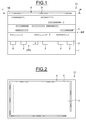
- the figure 1 illustrates an integrated circuit CI
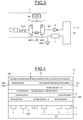
- the figure 2 is a partial sectional view along the section line II-II of the figure 1 .
- the integrated circuit CI comprises a semiconductor substrate 1, in which a plurality of components 2 has been produced in a zone Z of the integrated circuit. In this example, all the components of the integrated circuit CI are included in zone Z.
- the components here include logic gates, forming for example a cryptographic circuit CRY intended in particular to perform operations in a secure manner.
- the substrate 1 is surmounted by an interconnection region INT (known to those skilled in the art under the acronym BEOL: "Back End Of Line”), comprising several levels of metal each comprising one or more metal tracks 3 embedded in an insulating material ("Intermetal dielectric” according to an Anglo-Saxon name well known to those skilled in the art).
- INT interconnection region
- BEOL Back End Of Line
- Some of the metallic tracks 3 of the metal levels are interconnection tracks connecting at least some of the components 2 of the zone Z of the integrated circuit to each other via vias (not shown for simplification purposes).
- metal tracks may for example be redistribution tracks of the power supply or be connected to ground.
- the metallization level six N6 which here is the highest level, comprises a single metal track 31 which is not directly coupled to components of the cryptographic circuit CRY, but as will be seen below, forms an emitting antenna 5 coupled via vias to generation means 4 made in and on the substrate 1 and configured to generate an electrical signal SE which has a pseudo-random characteristic.
- generation means 4 and the antenna 5 form here an example of electromagnetic interference device.
- the level six of metallization N6 is not therefore an interconnection level because it does not comprise a metal track 3 connecting at least some of the components 2 of the zone Z of the circuit between them, but it is nevertheless realized according to the same process as that used to achieve the different levels of metal.
- the level six of metallization N6 includes metallic tracks interconnection extending for example inside the perimeter delimited by the metal track 31.
- the transmitting antenna 5 could comprise a plurality of metal loops located at different metallization levels and connected by vias.
- the figure 3 is a schematic representation of an exemplary embodiment of the generating means 4 of the electric signal SE.
- the transmitting antenna 5 comprises the metal track 31, a first end of which is coupled to a buffer element 6 ("Buffer" according to the English name) conventionally serving to amplify and shape the signal SE generated by the generating means 4 .
- Buffer according to the English name
- a capacitive element 7 is coupled between a second end of the metal track 31 and the ground GND.
- the capacitive element is used here to draw a current towards GND ground.
- the buffer element 6 and the capacitive element 7 are components made in and / or on the semiconductor substrate 1, and are electrically connected to the first metal track 31 via vias.
- the generation means 4 of the electrical signal SE comprise a generator H capable of delivering a clock signal CLK whose output is coupled to a delay circuit RT, and a pseudo-random value generator RDM whose output is also coupled to the RT delay circuit.
- generator H can also be used here by the cryptographic circuit CRY.
- the delay circuit RT comprises for example a delay line LRT configured to apply a delay to the rising edges of the clock signal CLK.
- This delay line LRT is connected via a first multiplexer MX1 to the output of the generator H and connected via a second multiplexer MX2 to the input of the buffer element 6.
- a direct path that is to say without delay, is also connected between the other inputs of the two multiplexers.
- multiplexers MX1 and MX2 are controlled by the binary value 0 or 1 delivered by the pseudo-random value generator RDM.
- the delay circuit RT may or may not select the delay line LRT, so that at least some of the rising edges of the clock signal CLK are delayed or not delayed so that pseudorandom.
- the delay of the delay line LRT is fixed (constant)
- the metal track 31 of the antenna 5 generates additional electromagnetic signals in a pseudo-random manner which, by adding to the electromagnetic signals emitted by the metal tracks 3, make it more difficult to analyze the overall electromagnetic signature of the integrated circuit CI.
- the integrated circuit CI comprises a second antenna 8 comprising a second metal track 32 located in the level five of metal N5 and coupled to a second buffer element 9 and a second capacitive element 10.
- the second metal track 32 is located above a sub-zone Z1 of the zone Z of the integrated circuit.
- the level five N5 metal further comprises here one or more metal tracks 320 for interconnecting logic components CRY cryptographic circuit.
- the electromagnetic interference device comprises selection means 15 coupled to the generation means 4 and to the first and second antennas 5 and 8.
- the selection means 15 comprise in this exemplary embodiment a control register CR, a first logic gate 11 of the "AND” type and a second logic gate 12 of the “AND” type, and are configured to select the antenna or antennas that will receive the electrical signal SE.
- the two logic gates 11 and 12 each comprise two inputs, a first input of which is coupled to the control register CR, and a second input is coupled to the output of the generation means 4.
- the first logic gate 11 has an output coupled to the first antenna 5 and the second logic gate 12 has an output coupled to the second antenna 8.
- control register CR sets the first inputs of the logic gates coupled to the antennas it selects, so that when generating a rising edge of the electrical signal SE, only the logic gates selected by the control register CR transmit the electrical signal SE to the antenna associated with them.
- control register CR may depend on the operations performed by the cryptographic circuit CRY, or alternatively, be carried out in a pseudo-random manner so as to further jam electromagnetic emissions.
- the integrated circuit CI comprises a first antenna 13 comprising a first metal track 33 situated in the metallization level six N6, above a first sub-zone Z2 of the zone Z of the integrated circuit CI, and a second antenna 14 comprising a second metal track 34 located in the second metallization level N2 above a second sub-zone Z3 of the integrated circuit CI, distinct from the second sub-zone Z2.
- the zone Z of the integrated circuit CI further comprises other components not included in the subzones Z2 and Z3 and above which there is no transmitting antenna.
- pseudo-random characteristic of the electrical signal SE described above was the signal form factor, it would be possible to envisage other characteristics of the signal that could be modified in a pseudo-random manner, such as, for example its amplitude and / or phase.
Landscapes
- Engineering & Computer Science (AREA)
- Physics & Mathematics (AREA)
- Signal Processing (AREA)
- Computer Networks & Wireless Communication (AREA)
- Computer Security & Cryptography (AREA)
- Theoretical Computer Science (AREA)
- Computer Hardware Design (AREA)
- General Physics & Mathematics (AREA)
- Electromagnetism (AREA)
- General Engineering & Computer Science (AREA)
- Nonlinear Science (AREA)
- Microelectronics & Electronic Packaging (AREA)
- Mathematical Physics (AREA)
- Software Systems (AREA)
- Semiconductor Integrated Circuits (AREA)
- Geometry (AREA)
Abstract
Description
- Des modes de mise en oeuvre et de réalisation de l'invention concernent les circuits intégrés, notamment mais non exclusivement ceux comportant des modules sécurisés, et en particulier la protection de ce type de circuit contre les analyses par canaux auxiliaires, connues par l'homme du métier sous la dénomination anglo-saxonne « Side channel analysis », et tout particulièrement contre les analyses des signaux électromagnétiques produits par le circuit intégré lors de son fonctionnement.
- En fonctionnement, un circuit intégré produit des signaux électromagnétiques par l'intermédiaire des pistes métalliques du circuit intégré, par exemple lors des commutations de ses composants logiques. En analysant ces signaux électromagnétiques, à l'aide par exemple d'une antenne et d'algorithmes mathématiques dédiés, il est possible d'obtenir des informations sur les opérations effectuées ainsi que sur les données manipulées et/ou sur leurs occurrences.
- Il est donc recommandé de brouiller autant que possible les signaux électromagnétiques émis par le circuit intégré.
- Ainsi, selon un mode de mise en oeuvre et de réalisation, il est proposé un procédé et un dispositif permettant de brouiller les émissions électromagnétiques d'un circuit intégré de manière à rendre encore plus difficile une éventuelle déduction des opérations effectuées par le circuit intégré.
- Selon un aspect, il est proposé un procédé de brouillage d'un rayonnement électromagnétique émis par une partie d'une région d'interconnexion située au dessus d'au moins une zone d'un circuit électronique intégré réalisé dans et/ou sur un substrat semi-conducteur, le procédé comprenant une disposition d'au moins une antenne métallique au dessus de ladite au moins une zone du circuit intégré et une circulation dans ladite au moins une antenne d'un signal électrique comportant au moins une caractéristique pseudo-aléatoire.
- En d'autres termes, on diminue le rapport signal sur bruit du circuit en ajoutant une source d'émissions électromagnétiques indépendante de la logique du circuit intégré, de manière à rendre plus difficile l'analyse des signaux électromagnétiques globaux émis par le circuit intégré et donc à rendre plus difficile une observation du fonctionnement du circuit par une analyse par canal auxiliaire.
- La circulation du signal électrique peut comprendre la génération d'un signal d'horloge, une application pseudo-aléatoire d'un retard, fixe ou variable, sur certains au moins des fronts dudit signal d'horloge de façon à obtenir ledit signal électrique, et une transmission dudit signal électrique dans l'antenne.
- On obtient ainsi un signal électrique ayant ici un facteur de forme (ladite au moins une caractéristique) pseudo-aléatoire.
- Selon un mode de mise en oeuvre, on peut disposer une première antenne et au moins une deuxième antenne au dessus de ladite au moins une zone du circuit intégré, le procédé pouvant alors comprendre une sélection d'au moins une desdites antennes, et une circulation dudit signal électrique dans ladite au moins une antenne sélectionnée.
- Selon un autre aspect, il est proposé un dispositif de brouillage d'un rayonnement électromagnétique émis par au moins une partie d'une région d'interconnexion située au dessus d'au moins une zone d'un circuit électronique intégré réalisé dans et/ou sur un substrat semi-conducteur comprenant au moins une antenne située au dessus de ladite au moins une zone du circuit, et des moyens de génération configurés pour générer un signal électrique comportant au moins une caractéristique pseudo-aléatoire et couplés à ladite au moins une antenne.
- Les moyens de génération peuvent comprendre un générateur configuré pour générer un signal d'horloge et des moyens pour appliquer de façon pseudo-aléatoire un retard, fixe ou variable, sur certains au moins des fronts dudit signal d'horloge.
- La partie d'interconnexion peut comprendre plusieurs niveaux de métallisation dont au moins un niveau de métallisation comprend au moins une piste métallique formant au moins une partie de ladite au moins une antenne.
- Selon un mode de réalisation, le dispositif peut comprendre une première antenne et au moins une deuxième antenne, le dispositif comprenant des moyens de sélection configurés pour sélectionner au moins l'une desdites première et deuxième antennes de façon à délivrer ledit signal électrique à ladite au moins une antenne sélectionnée.
- La première antenne et ladite au moins une deuxième antenne peuvent être situées dans un même niveau de métallisation de la région d'interconnexion du circuit, ou dans des niveaux de métallisation distincts.
- Selon un mode de réalisation, la première antenne peut être située au dessus d'une première zone du circuit intégré et la dite au moins une deuxième antenne peut être située au dessus d'une deuxième zone du circuit intégré distincte de la première zone.
- Selon un autre mode de réalisation, la première antenne peut être située au dessus d'une première zone du circuit intégré et ladite au moins une deuxième antenne peut être située au moins en partie au dessus de ladite au moins une première zone.
- Les moyens de sélection peuvent comprendre un registre de contrôle et des portes logiques couplées entre lesdites antennes et ledit registre de contrôle.
- D'autres avantages et caractéristiques de l'invention apparaîtront à l'examen de la description détaillée de modes de mise en oeuvre et de réalisation de l'invention, nullement limitatifs, et des dessins annexés sur lesquels :
- les
figures 1 à 6 illustrent des modes de mise en oeuvre et de réalisation de l'invention. - La
figure 1 illustre un circuit intégré CI, et lafigure 2 est une vue partielle en coupe selon la ligne de coupe II-II de lafigure 1 . - Le circuit intégré CI comporte un substrat semi-conducteur 1, dans lequel une pluralité de composants 2 a été réalisée dans une zone Z du circuit intégré. Dans cet exemple, tous les composants du circuit intégré CI sont compris dans la zone Z.
- Les composants comportent ici notamment des portes logiques, formant par exemple un circuit cryptographique CRY destiné notamment à réaliser des opérations de manière sécurisée.
- Le substrat 1 est surmonté par une région d'interconnexion INT (connue par l'homme du métier sous l'acronyme anglo-saxon BEOL : « Back End Of Line »), comportant plusieurs niveaux de métal comportant chacun une ou plusieurs pistes métalliques 3 enrobées dans un matériau isolant (« Intermetal dielectric » selon une dénomination anglo-saxonne bien connue de l'homme du métier).
- Certaines des pistes métalliques 3 des niveaux de métal sont des pistes d'interconnexion reliant certains au moins des composants 2 de la zone Z du circuit intégré entre eux par l'intermédiaire de vias (non représentées à des fins de simplification).
- D'autres pistes métalliques peuvent être par exemple des pistes de redistribution de l'alimentation ou être reliées à la masse.
- Le niveau six N6 de métallisation, qui ici est le niveau le plus haut, comporte une unique piste métallique 31 qui n'est pas directement couplée à des composants du circuit cryptographique CRY, mais comme il sera vu ci-après, forme une antenne émettrice 5 couplée par l'intermédiaire de vias à des moyens de génération 4 réalisés dans et sur le substrat 1 et configurés pour générer un signal électrique SE qui comporte une caractéristique pseudo-aléatoire. Ces moyens de génération 4 et l'antenne 5 forment ici un exemple de dispositif de brouillage électromagnétique.
- Dans cet exemple, le niveau six de métallisation N6 n'est donc pas un niveau d'interconnexion car il ne comporte pas de piste métallique 3 reliant certains au moins des composants 2 de la zone Z du circuit entre eux, mais il est toutefois réalisé selon le même procédé que celui utilisé pour réaliser les différents niveaux de métal.
- Cela étant, il serait tout à fait possible d'envisager que le niveau six de métallisation N6 comporte des pistes métalliques d'interconnexion s'étendant par exemple à l'intérieur du périmètre délimité par la piste métallique 31.
- Il convient de noter que l'antenne émettrice 5 pourrait comprendre plusieurs boucles métalliques situées à des niveaux de métallisations différents et reliées par des vias.
- La
figure 3 est une représentation schématique d'un exemple de réalisation des moyens de génération 4 du signal électrique SE. - L'antenne émettrice 5 comporte la piste métallique 31 dont une première extrémité est couplée à un élément tampon 6 (« Buffer » selon la dénomination anglo-saxonne) servant classiquement à amplifier et mettre en forme le signal SE généré par les moyens de génération 4.
- Un élément capacitif 7 est couplé entre une seconde extrémité de la piste métallique 31 et la masse GND. L'élément capacitif est ici utilisé pour tirer un courant vers la masse GND.
- L'élément tampon 6 et l'élément capacitif 7 sont des composants réalisés dans et/ou sur le substrat semi-conducteur 1, et sont électriquement connectés à la première piste métallique 31 par des vias.
- Les moyens de génération 4 du signal électrique SE comprennent un générateur H apte à délivrer un signal d'horloge CLK dont la sortie est couplée à un circuit de retard RT, et un générateur de valeurs pseudo-aléatoires RDM dont la sortie est également couplée au circuit de retard RT.
- Il convient de noter que le générateur H peut être ici également utilisé par le circuit cryptographique CRY.
- Le circuit de retard RT comporte par exemple une ligne à retard LRT configurée pour appliquer un retard aux fronts montants du signal d'horloge CLK.
- Cette ligne à retard LRT est connectée par l'intermédiaire d'un premier multiplexeur MX1 à la sortie du générateur H et connectée par l'intermédiaire d'un deuxième multiplexeur MX2 à l'entrée de l'élément tampon 6.
- Un chemin direct, c'est-à-dire sans retard, est également connecté entre les autres entrées des deux multiplexeurs.
- Ces multiplexeurs MX1 et MX2 sont commandés par la valeur binaire 0 ou 1 délivrée par le générateur de valeurs pseudo-aléatoires RDM.
- En fonction de la valeur générée par le générateur RDM, le circuit de retard RT peut ou non sélectionner la ligne à retard LRT, de manière à ce que certains au moins des fronts montants du signal d'horloge CLK soient retardés ou non retardés de façon pseudo-aléatoire.
- Alors que dans ce mode de réalisation le retard de la ligne à retard LRT est fixe (constant), il serait possible, en variante, de prévoir une ligne à retard configurée pour avoir un retard variable, par exemple de façon pseudo-aléatoire, en fonction de la valeur logique délivrée par un autre générateur de nombres pseudo-aléatoires.
- Ainsi, de la même manière que les pistes métalliques d'interconnexion 3 génèrent des signaux électromagnétiques en fonction des opérations effectuées par le circuit cryptographique CRY, la piste métallique 31 de l'antenne 5 génère des signaux électromagnétiques additionnels de façon pseudo-aléatoire qui, en s'ajoutant aux signaux électromagnétiques émis par les pistes métalliques 3, rendent plus difficile l'analyse de la signature électromagnétique globale du circuit intégré CI.
- Selon un autre mode de réalisation illustré sur les
figures 4 et5 , le circuit intégré CI comporte une deuxième antenne 8 comportant une deuxième piste métallique 32 située dans le niveau cinq de métal N5 et couplée à un deuxième élément tampon 9 et à un deuxième élément capacitif 10. La deuxième piste métallique 32 est située au dessus d'une sous-zone Z1 de la zone Z du circuit intégré. - Le niveau cinq N5 de métal comprend en outre ici une ou plusieurs pistes de métal 320 permettant l'interconnexion de composants logique du circuit cryptographique CRY.
- Comme l'illustre la
figure 5 , le dispositif de brouillage électromagnétique comporte des moyens de sélection 15 couplés aux moyens de génération 4 et aux première et deuxième antennes 5 et 8. - Les moyens de sélection 15 comprennent dans cet exemple de réalisation un registre de contrôle CR, une première porte logique 11 de type « ET » et une deuxième porte logique 12 de type « ET », et sont configurés pour sélectionner la ou les antennes qui recevront le signal électrique SE.
- Les deux portes logiques 11 et 12 comportent chacune deux entrées, dont une première entrée est couplée au registre de contrôle CR, et une deuxième entrée est couplée à la sortie des moyens de génération 4.
- La première porte logique 11 comporte une sortie couplée à la première antenne 5 et la deuxième porte logique 12 comporte une sortie couplée à la deuxième antenne 8.
- Ainsi, lors du fonctionnement du circuit, le registre de contrôle CR met à un les premières entrées des portes logiques couplées aux antennes qu'il sélectionne, de manière à ce que lors de la génération d'un front montant du signal électrique SE, seules les portes logiques sélectionnées par le registre de contrôle CR transmettent le signal électrique SE à l'antenne qui leur est associée.
- La sélection des antennes par le registre de contrôle CR peut dépendre des opérations effectuées par le circuit cryptographique CRY, ou en variante, se faire de manière pseudo-aléatoire de façon à brouiller encore davantage les émissions électromagnétiques.
- Selon une variante illustrée sur la
figure 6 , le circuit intégré CI comporte une première antenne 13 comportant une première piste métallique 33 située dans le niveau six N6 de métallisation, au dessus d'une première sous-zone Z2 de la zone Z du circuit intégré CI, et une deuxième antenne 14 comportant une deuxième piste métallique 34 située dans le niveau deux N2 de métallisation au dessus d'une deuxième sous-zone Z3 du circuit intégré CI, distincte de la deuxième sous-zone Z2. - La zone Z du circuit intégré CI comporte en outre d'autres composants non compris dans les sous-zones Z2 et Z3 et au dessus desquels ne se trouve pas d'antenne émettrice.
- Il convient de noter que les modes de mise en oeuvre et de réalisation présentés ici ne sont nullement limitatifs. Notamment, bien qu'il ait été présenté ici des circuits intégrés comportant une ou deux antennes, il est tout à fait possible d'envisager un circuit intégré comportant un nombre plus important d'antennes, dont les pistes métalliques sont situées dans un ou plusieurs niveaux de métal, au dessus d'une ou plusieurs zones du circuit intégré.
- Par ailleurs alors que la caractéristique pseudo-aléatoire du signal électrique SE décrite ci-avant était le facteur de forme du signal, il serait possible d'envisager d'autres caractéristiques du signal qui pourraient être modifiées de façon pseudo-aléatoire, comme par exemple son amplitude et/ou sa phase.
Claims (14)
- Procédé de brouillage d'un rayonnement électromagnétique émis par une partie d'une région d'interconnexion (INT) située au dessus d'au moins une zone (Z) d'un circuit électronique intégré (CI) réalisé dans et/ou sur un substrat semi-conducteur (1), comprenant une disposition d'au moins une antenne métallique (5) au dessus de ladite au moins une zone (Z) du circuit intégré (CI) et une circulation dans ladite au moins une antenne (5) d'un signal électrique (SE) comportant au moins une caractéristique pseudo-aléatoire.
- Procédé selon la revendication 1, dans lequel la circulation dudit signal électrique (SE) comprend la génération d'un signal d'horloge (CLK), une application pseudo-aléatoire d'un retard sur certains au moins des fronts dudit signal d'horloge (CLK) de façon à obtenir ledit signal électrique (SE), et une transmission dudit signal électrique (SE) dans l'antenne (5).
- Procédé selon la revendication 1 ou 2, dans lequel le retard est fixe ou variable.
- Procédé selon la revendication 1 à 3, dans lequel on dispose une première antenne (5) et au moins une deuxième antenne (8) au dessus de ladite au moins une zone (Z) du circuit intégré (CI), le procédé comprenant en outre une sélection d'au moins une desdites antennes (5, 8), et une circulation dudit signal électrique (SE) dans ladite au moins une antenne sélectionnée (5, 8).
- Dispositif de brouillage d'un rayonnement électromagnétique susceptible d'être émis par au moins une partie d'une région d'interconnexion (INT) située au dessus d'au moins une zone (Z) d'un circuit électronique intégré (CI) réalisé dans et/ou sur un substrat semi-conducteur (1) comprenant au moins une antenne (5) située au dessus de ladite au moins une zone (Z) du circuit (CI), et des moyens de génération (4) configurés pour générer un signal électrique (SE) comportant au moins une caractéristique pseudo-aléatoire et couplés à ladite au moins une antenne (5).
- Dispositif selon la revendication 5, dans lequel les moyens de génération (4) comprennent un générateur (H) configuré pour générer un signal d'horloge (CLK) et des moyens de retard (RT, RDM) pour appliquer de façon pseudo-aléatoire un retard sur certains au moins des fronts dudit signal d'horloge (CLK).
- Dispositif selon la revendication 5 ou 6, dans lequel les moyens de retard (RT, RDM) sont configurés pour appliquer de façon pseudo-aléatoire un retard fixe ou variable sur certains au moins des fronts dudit signal d'horloge (CLK).
- Dispositif selon l'une des revendications 5 à 7, dans lequel la région d'interconnexion (INT) comprend plusieurs niveaux de métallisation dont au moins un niveau de métallisation (N6) comprend au moins une piste métallique (31) formant au moins une partie de ladite au moins une antenne (5).
- Dispositif selon l'une quelconque des revendications 5 à 8, comprenant une première antenne (5) et au moins une deuxième antenne (8), le dispositif comprenant des moyens de sélection (15) configurés pour sélectionner au moins l'une desdites première et deuxième antennes (5, 8) de façon à délivrer ledit signal électrique (SE) à ladite au moins une antenne sélectionnée.
- Dispositif selon la revendication 9, dans lequel la première antenne et ladite au moins une deuxième antenne sont situées dans un même niveau de métallisation de la région d'interconnexion du circuit.
- Dispositif selon la revendication 9, dans lequel la première antenne (5) et ladite au moins une deuxième antenne (8), sont situées dans des niveaux de métallisation (N6, N5) distincts.
- Dispositif selon la revendication 10 ou 11, dans lequel la première antenne (13) est située au dessus d'une première zone (Z2) du circuit intégré et ladite au moins une deuxième antenne (14) est située au dessus d'une deuxième zone (Z3) du circuit intégré distincte de la première zone (Z2).
- Dispositif selon la revendication 10 ou 11, dans lequel la première antenne (5) est située au dessus d'une première zone (Z) du circuit intégré (CI) et ladite au moins une deuxième antenne (8) est située au moins en partie au dessus de ladite au moins une première zone (Z).
- Dispositif selon l'une quelconque des revendications 9 à 13, dans lequel les moyens de sélection (15) comprennent un registre de contrôle (CR) et des portes logiques (11, 12) couplées entre lesdites antennes (5, 8) et ledit registre de contrôle (CR).
Applications Claiming Priority (1)
| Application Number | Priority Date | Filing Date | Title |
|---|---|---|---|
| FR1651552A FR3048296B1 (fr) | 2016-02-25 | 2016-02-25 | Procede et dispositif de brouillage electromagnetique pour circuit integre |
Publications (2)
| Publication Number | Publication Date |
|---|---|
| EP3211626A1 true EP3211626A1 (fr) | 2017-08-30 |
| EP3211626B1 EP3211626B1 (fr) | 2018-10-31 |
Family
ID=56372957
Family Applications (1)
| Application Number | Title | Priority Date | Filing Date |
|---|---|---|---|
| EP16181835.6A Active EP3211626B1 (fr) | 2016-02-25 | 2016-07-29 | Procédé et dispositif de brouillage électromagnétique pour circuit intégré |
Country Status (4)
| Country | Link |
|---|---|
| US (1) | US10148421B2 (fr) |
| EP (1) | EP3211626B1 (fr) |
| CN (3) | CN107123638B (fr) |
| FR (1) | FR3048296B1 (fr) |
Cited By (1)
| Publication number | Priority date | Publication date | Assignee | Title |
|---|---|---|---|---|
| EP3418937A1 (fr) * | 2017-06-22 | 2018-12-26 | STMicroelectronics (Rousset) SAS | Procédé pour créer un leurre d'un fonctionnement d'un circuit intégré et circuit intégré correspondant |
Families Citing this family (1)
| Publication number | Priority date | Publication date | Assignee | Title |
|---|---|---|---|---|
| FR3048296B1 (fr) * | 2016-02-25 | 2018-03-30 | Stmicroelectronics (Rousset) Sas | Procede et dispositif de brouillage electromagnetique pour circuit integre |
Citations (3)
| Publication number | Priority date | Publication date | Assignee | Title |
|---|---|---|---|---|
| US20110246789A1 (en) * | 2010-03-31 | 2011-10-06 | Inside Contactless | Integrated circuit protected against horizontal side channel analysis |
| EP2587469A1 (fr) * | 2011-10-27 | 2013-05-01 | Certicom Corp. | Circuit intégré doté de circuits logiques et de circuits d'occultation multiples |
| US20130321053A1 (en) * | 2012-05-30 | 2013-12-05 | Infineon Technologies Austria Ag | Method and device for sampling an input signal |
Family Cites Families (13)
| Publication number | Priority date | Publication date | Assignee | Title |
|---|---|---|---|---|
| US4467328A (en) * | 1981-10-26 | 1984-08-21 | Westinghouse Electric Corp. | Radar jammer with an antenna array of pseudo-randomly spaced radiating elements |
| JP3296341B2 (ja) * | 1999-09-20 | 2002-06-24 | 日本電気株式会社 | 相関器 |
| JP2002319011A (ja) * | 2001-01-31 | 2002-10-31 | Canon Inc | 半導体装置、半導体装置の製造方法及び電子写真装置 |
| US6907234B2 (en) * | 2001-10-26 | 2005-06-14 | Microsoft Corporation | System and method for automatically tuning an antenna |
| US20060111054A1 (en) * | 2004-11-22 | 2006-05-25 | Interdigital Technology Corporation | Method and system for selecting transmit antennas to reduce antenna correlation |
| US7343265B2 (en) * | 2005-11-23 | 2008-03-11 | Lockheed Martin Corporation | System to monitor the health of a structure, sensor nodes, program product, and related methods |
| JP2008083679A (ja) * | 2006-08-31 | 2008-04-10 | Seiko Epson Corp | 表示装置および電子機器 |
| JP4840230B2 (ja) * | 2007-03-30 | 2011-12-21 | ブラザー工業株式会社 | 無線ネットワークシステム、およびそれを構成するための無線機器 |
| US7907275B2 (en) * | 2009-06-19 | 2011-03-15 | Hewlett-Packard Development Company, L.P. | Type selective and polarization selective device for Raman spectroscopy |
| EP2365659B1 (fr) * | 2010-03-01 | 2017-04-12 | Inside Secure | Procédé de test de la résistance d'un circuit intégré à une analyse par canal auxiliaire |
| US8427194B2 (en) * | 2010-05-24 | 2013-04-23 | Alexander Roger Deas | Logic system with resistance to side-channel attack by exhibiting a closed clock-data eye diagram |
| US10018716B2 (en) * | 2014-06-26 | 2018-07-10 | Honeywell International Inc. | Systems and methods for calibration and optimization of frequency modulated continuous wave radar altimeters using adjustable self-interference cancellation |
| FR3048296B1 (fr) * | 2016-02-25 | 2018-03-30 | Stmicroelectronics (Rousset) Sas | Procede et dispositif de brouillage electromagnetique pour circuit integre |
-
2016
- 2016-02-25 FR FR1651552A patent/FR3048296B1/fr not_active Expired - Fee Related
- 2016-07-28 US US15/221,749 patent/US10148421B2/en active Active
- 2016-07-29 EP EP16181835.6A patent/EP3211626B1/fr active Active
- 2016-08-22 CN CN201610703470.3A patent/CN107123638B/zh active Active
- 2016-08-22 CN CN201620918705.6U patent/CN206116394U/zh not_active Withdrawn - After Issue
- 2016-08-22 CN CN201910461121.9A patent/CN110263897B/zh active Active
Patent Citations (3)
| Publication number | Priority date | Publication date | Assignee | Title |
|---|---|---|---|---|
| US20110246789A1 (en) * | 2010-03-31 | 2011-10-06 | Inside Contactless | Integrated circuit protected against horizontal side channel analysis |
| EP2587469A1 (fr) * | 2011-10-27 | 2013-05-01 | Certicom Corp. | Circuit intégré doté de circuits logiques et de circuits d'occultation multiples |
| US20130321053A1 (en) * | 2012-05-30 | 2013-12-05 | Infineon Technologies Austria Ag | Method and device for sampling an input signal |
Cited By (2)
| Publication number | Priority date | Publication date | Assignee | Title |
|---|---|---|---|---|
| EP3418937A1 (fr) * | 2017-06-22 | 2018-12-26 | STMicroelectronics (Rousset) SAS | Procédé pour créer un leurre d'un fonctionnement d'un circuit intégré et circuit intégré correspondant |
| FR3068153A1 (fr) * | 2017-06-22 | 2018-12-28 | Stmicroelectronics (Rousset) Sas | Procede pour creer un leurre d'un fonctionnement d'un circuit integre et circuit integre correspondant |
Also Published As
| Publication number | Publication date |
|---|---|
| FR3048296A1 (fr) | 2017-09-01 |
| CN110263897B (zh) | 2022-11-22 |
| US20170250795A1 (en) | 2017-08-31 |
| CN110263897A (zh) | 2019-09-20 |
| CN107123638A (zh) | 2017-09-01 |
| CN206116394U (zh) | 2017-04-19 |
| CN107123638B (zh) | 2019-06-21 |
| FR3048296B1 (fr) | 2018-03-30 |
| EP3211626B1 (fr) | 2018-10-31 |
| US10148421B2 (en) | 2018-12-04 |
Similar Documents
| Publication | Publication Date | Title |
|---|---|---|
| EP3264460B1 (fr) | Procédé de protection d'un circuit intégré, et circuit intégré correspondant | |
| FR2786961A1 (fr) | Dispositif electronique pour systeme de cablage de bus | |
| WO2007110506A1 (fr) | Generateur de nombres aleatoires | |
| EP3211626B1 (fr) | Procédé et dispositif de brouillage électromagnétique pour circuit intégré | |
| EP4280094A1 (fr) | Generateur de nombres aleatoires a transistors double grilles fd-soi lvt polarises en mode fbb | |
| FR2488006A1 (fr) | Circuit de report perfectionne pour un additionneur binaire | |
| EP3418937B1 (fr) | Procédé pour créer un leurre d'un fonctionnement d'un circuit intégré et circuit intégré correspondant | |
| EP3483773B1 (fr) | Procédé de modification aléatoire du profil de consommation d'un circuit logique, et dispositif associé | |
| FR2929470A1 (fr) | Procede de protection de circuit de cryptographie programmable, et circuit protege par un tel procede | |
| FR3112004A1 (fr) | Détection d'une impulsion électromagnétique | |
| FR2494040A1 (fr) | Dispositif a circuits integres a semiconducteurs proteges contre les surtensions accidentelles | |
| FR3084226A1 (fr) | Architecture emettrice radiofrequence rf | |
| WO2005059999A1 (fr) | Circuit integre protege par bouclier actif | |
| EP2624296A1 (fr) | Protection d'un circuit integre contre des attaques invasives | |
| EP1376149A1 (fr) | Procédé et dispositif de commande d'un générateur d'impulsions pour l'émission d'un signal impulsionnel du type à bande ultra large modulé en position | |
| EP0412855B1 (fr) | Transducteurs électrique/acoustique et acoustique/électrique pour dispositif à ondes de surface à diffraction réduite et dispositif à ondes de surface correspondant | |
| FR3071101A1 (fr) | Empilement de puces | |
| EP0208588A1 (fr) | Alimentation électrique | |
| WO2006117391A1 (fr) | Dispositif formant porte logique adaptee pour minimiser les differences de comportement electrique ou electromagnetique dans un circuit integre manipulant un secret | |
| FR3123743A1 (fr) | Circuit électronique de multiplication et procédé correspondant de multiplication au sein d’un tel circuit | |
| EP0849659B1 (fr) | Dispositif numérique d'initialisation d'un circuit intégré | |
| FR2856196A1 (fr) | Composant electronique protege contre les decharges electrostatiques | |
| WO2013121149A1 (fr) | Procédé et dispositif électronique de génération d'un signal d'horloge variable | |
| FR2847715A1 (fr) | Circuit integre comportant des sous-ensembles connectes en serie | |
| FR3155102A1 (fr) | Dispositif émetteur de charge sans fil |
Legal Events
| Date | Code | Title | Description |
|---|---|---|---|
| PUAI | Public reference made under article 153(3) epc to a published international application that has entered the european phase |
Free format text: ORIGINAL CODE: 0009012 |
|
| STAA | Information on the status of an ep patent application or granted ep patent |
Free format text: STATUS: REQUEST FOR EXAMINATION WAS MADE |
|
| 17P | Request for examination filed |
Effective date: 20160729 |
|
| AK | Designated contracting states |
Kind code of ref document: A1 Designated state(s): AL AT BE BG CH CY CZ DE DK EE ES FI FR GB GR HR HU IE IS IT LI LT LU LV MC MK MT NL NO PL PT RO RS SE SI SK SM TR |
|
| AX | Request for extension of the european patent |
Extension state: BA ME |
|
| GRAP | Despatch of communication of intention to grant a patent |
Free format text: ORIGINAL CODE: EPIDOSNIGR1 |
|
| STAA | Information on the status of an ep patent application or granted ep patent |
Free format text: STATUS: GRANT OF PATENT IS INTENDED |
|
| INTG | Intention to grant announced |
Effective date: 20180607 |
|
| GRAJ | Information related to disapproval of communication of intention to grant by the applicant or resumption of examination proceedings by the epo deleted |
Free format text: ORIGINAL CODE: EPIDOSDIGR1 |
|
| STAA | Information on the status of an ep patent application or granted ep patent |
Free format text: STATUS: REQUEST FOR EXAMINATION WAS MADE |
|
| GRAR | Information related to intention to grant a patent recorded |
Free format text: ORIGINAL CODE: EPIDOSNIGR71 |
|
| GRAS | Grant fee paid |
Free format text: ORIGINAL CODE: EPIDOSNIGR3 |
|
| STAA | Information on the status of an ep patent application or granted ep patent |
Free format text: STATUS: GRANT OF PATENT IS INTENDED |
|
| GRAA | (expected) grant |
Free format text: ORIGINAL CODE: 0009210 |
|
| STAA | Information on the status of an ep patent application or granted ep patent |
Free format text: STATUS: THE PATENT HAS BEEN GRANTED |
|
| INTC | Intention to grant announced (deleted) | ||
| INTG | Intention to grant announced |
Effective date: 20180913 |
|
| AK | Designated contracting states |
Kind code of ref document: B1 Designated state(s): AL AT BE BG CH CY CZ DE DK EE ES FI FR GB GR HR HU IE IS IT LI LT LU LV MC MK MT NL NO PL PT RO RS SE SI SK SM TR |
|
| REG | Reference to a national code |
Ref country code: CH Ref legal event code: EP Ref country code: GB Ref legal event code: FG4D Free format text: NOT ENGLISH |
|
| REG | Reference to a national code |
Ref country code: AT Ref legal event code: REF Ref document number: 1060341 Country of ref document: AT Kind code of ref document: T Effective date: 20181115 |
|
| REG | Reference to a national code |
Ref country code: IE Ref legal event code: FG4D Free format text: LANGUAGE OF EP DOCUMENT: FRENCH |
|
| REG | Reference to a national code |
Ref country code: DE Ref legal event code: R096 Ref document number: 602016006745 Country of ref document: DE |
|
| REG | Reference to a national code |
Ref country code: NL Ref legal event code: MP Effective date: 20181031 |
|
| REG | Reference to a national code |
Ref country code: LT Ref legal event code: MG4D |
|
| REG | Reference to a national code |
Ref country code: AT Ref legal event code: MK05 Ref document number: 1060341 Country of ref document: AT Kind code of ref document: T Effective date: 20181031 |
|
| PG25 | Lapsed in a contracting state [announced via postgrant information from national office to epo] |
Ref country code: LV Free format text: LAPSE BECAUSE OF FAILURE TO SUBMIT A TRANSLATION OF THE DESCRIPTION OR TO PAY THE FEE WITHIN THE PRESCRIBED TIME-LIMIT Effective date: 20181031 Ref country code: NO Free format text: LAPSE BECAUSE OF FAILURE TO SUBMIT A TRANSLATION OF THE DESCRIPTION OR TO PAY THE FEE WITHIN THE PRESCRIBED TIME-LIMIT Effective date: 20190131 Ref country code: LT Free format text: LAPSE BECAUSE OF FAILURE TO SUBMIT A TRANSLATION OF THE DESCRIPTION OR TO PAY THE FEE WITHIN THE PRESCRIBED TIME-LIMIT Effective date: 20181031 Ref country code: FI Free format text: LAPSE BECAUSE OF FAILURE TO SUBMIT A TRANSLATION OF THE DESCRIPTION OR TO PAY THE FEE WITHIN THE PRESCRIBED TIME-LIMIT Effective date: 20181031 Ref country code: AT Free format text: LAPSE BECAUSE OF FAILURE TO SUBMIT A TRANSLATION OF THE DESCRIPTION OR TO PAY THE FEE WITHIN THE PRESCRIBED TIME-LIMIT Effective date: 20181031 Ref country code: IS Free format text: LAPSE BECAUSE OF FAILURE TO SUBMIT A TRANSLATION OF THE DESCRIPTION OR TO PAY THE FEE WITHIN THE PRESCRIBED TIME-LIMIT Effective date: 20190228 Ref country code: BG Free format text: LAPSE BECAUSE OF FAILURE TO SUBMIT A TRANSLATION OF THE DESCRIPTION OR TO PAY THE FEE WITHIN THE PRESCRIBED TIME-LIMIT Effective date: 20190131 Ref country code: ES Free format text: LAPSE BECAUSE OF FAILURE TO SUBMIT A TRANSLATION OF THE DESCRIPTION OR TO PAY THE FEE WITHIN THE PRESCRIBED TIME-LIMIT Effective date: 20181031 Ref country code: HR Free format text: LAPSE BECAUSE OF FAILURE TO SUBMIT A TRANSLATION OF THE DESCRIPTION OR TO PAY THE FEE WITHIN THE PRESCRIBED TIME-LIMIT Effective date: 20181031 Ref country code: PL Free format text: LAPSE BECAUSE OF FAILURE TO SUBMIT A TRANSLATION OF THE DESCRIPTION OR TO PAY THE FEE WITHIN THE PRESCRIBED TIME-LIMIT Effective date: 20181031 |
|
| PG25 | Lapsed in a contracting state [announced via postgrant information from national office to epo] |
Ref country code: PT Free format text: LAPSE BECAUSE OF FAILURE TO SUBMIT A TRANSLATION OF THE DESCRIPTION OR TO PAY THE FEE WITHIN THE PRESCRIBED TIME-LIMIT Effective date: 20190301 Ref country code: NL Free format text: LAPSE BECAUSE OF FAILURE TO SUBMIT A TRANSLATION OF THE DESCRIPTION OR TO PAY THE FEE WITHIN THE PRESCRIBED TIME-LIMIT Effective date: 20181031 Ref country code: GR Free format text: LAPSE BECAUSE OF FAILURE TO SUBMIT A TRANSLATION OF THE DESCRIPTION OR TO PAY THE FEE WITHIN THE PRESCRIBED TIME-LIMIT Effective date: 20190201 Ref country code: AL Free format text: LAPSE BECAUSE OF FAILURE TO SUBMIT A TRANSLATION OF THE DESCRIPTION OR TO PAY THE FEE WITHIN THE PRESCRIBED TIME-LIMIT Effective date: 20181031 Ref country code: SE Free format text: LAPSE BECAUSE OF FAILURE TO SUBMIT A TRANSLATION OF THE DESCRIPTION OR TO PAY THE FEE WITHIN THE PRESCRIBED TIME-LIMIT Effective date: 20181031 Ref country code: RS Free format text: LAPSE BECAUSE OF FAILURE TO SUBMIT A TRANSLATION OF THE DESCRIPTION OR TO PAY THE FEE WITHIN THE PRESCRIBED TIME-LIMIT Effective date: 20181031 |
|
| PG25 | Lapsed in a contracting state [announced via postgrant information from national office to epo] |
Ref country code: DK Free format text: LAPSE BECAUSE OF FAILURE TO SUBMIT A TRANSLATION OF THE DESCRIPTION OR TO PAY THE FEE WITHIN THE PRESCRIBED TIME-LIMIT Effective date: 20181031 Ref country code: CZ Free format text: LAPSE BECAUSE OF FAILURE TO SUBMIT A TRANSLATION OF THE DESCRIPTION OR TO PAY THE FEE WITHIN THE PRESCRIBED TIME-LIMIT Effective date: 20181031 Ref country code: IT Free format text: LAPSE BECAUSE OF FAILURE TO SUBMIT A TRANSLATION OF THE DESCRIPTION OR TO PAY THE FEE WITHIN THE PRESCRIBED TIME-LIMIT Effective date: 20181031 |
|
| REG | Reference to a national code |
Ref country code: DE Ref legal event code: R097 Ref document number: 602016006745 Country of ref document: DE |
|
| PG25 | Lapsed in a contracting state [announced via postgrant information from national office to epo] |
Ref country code: RO Free format text: LAPSE BECAUSE OF FAILURE TO SUBMIT A TRANSLATION OF THE DESCRIPTION OR TO PAY THE FEE WITHIN THE PRESCRIBED TIME-LIMIT Effective date: 20181031 Ref country code: SM Free format text: LAPSE BECAUSE OF FAILURE TO SUBMIT A TRANSLATION OF THE DESCRIPTION OR TO PAY THE FEE WITHIN THE PRESCRIBED TIME-LIMIT Effective date: 20181031 Ref country code: EE Free format text: LAPSE BECAUSE OF FAILURE TO SUBMIT A TRANSLATION OF THE DESCRIPTION OR TO PAY THE FEE WITHIN THE PRESCRIBED TIME-LIMIT Effective date: 20181031 Ref country code: SK Free format text: LAPSE BECAUSE OF FAILURE TO SUBMIT A TRANSLATION OF THE DESCRIPTION OR TO PAY THE FEE WITHIN THE PRESCRIBED TIME-LIMIT Effective date: 20181031 |
|
| PLBE | No opposition filed within time limit |
Free format text: ORIGINAL CODE: 0009261 |
|
| STAA | Information on the status of an ep patent application or granted ep patent |
Free format text: STATUS: NO OPPOSITION FILED WITHIN TIME LIMIT |
|
| 26N | No opposition filed |
Effective date: 20190801 |
|
| PG25 | Lapsed in a contracting state [announced via postgrant information from national office to epo] |
Ref country code: SI Free format text: LAPSE BECAUSE OF FAILURE TO SUBMIT A TRANSLATION OF THE DESCRIPTION OR TO PAY THE FEE WITHIN THE PRESCRIBED TIME-LIMIT Effective date: 20181031 |
|
| PG25 | Lapsed in a contracting state [announced via postgrant information from national office to epo] |
Ref country code: MC Free format text: LAPSE BECAUSE OF FAILURE TO SUBMIT A TRANSLATION OF THE DESCRIPTION OR TO PAY THE FEE WITHIN THE PRESCRIBED TIME-LIMIT Effective date: 20181031 |
|
| REG | Reference to a national code |
Ref country code: CH Ref legal event code: PL |
|
| PG25 | Lapsed in a contracting state [announced via postgrant information from national office to epo] |
Ref country code: TR Free format text: LAPSE BECAUSE OF FAILURE TO SUBMIT A TRANSLATION OF THE DESCRIPTION OR TO PAY THE FEE WITHIN THE PRESCRIBED TIME-LIMIT Effective date: 20181031 |
|
| REG | Reference to a national code |
Ref country code: BE Ref legal event code: MM Effective date: 20190731 |
|
| PG25 | Lapsed in a contracting state [announced via postgrant information from national office to epo] |
Ref country code: LU Free format text: LAPSE BECAUSE OF NON-PAYMENT OF DUE FEES Effective date: 20190729 Ref country code: CH Free format text: LAPSE BECAUSE OF NON-PAYMENT OF DUE FEES Effective date: 20190731 Ref country code: LI Free format text: LAPSE BECAUSE OF NON-PAYMENT OF DUE FEES Effective date: 20190731 Ref country code: BE Free format text: LAPSE BECAUSE OF NON-PAYMENT OF DUE FEES Effective date: 20190731 |
|
| PG25 | Lapsed in a contracting state [announced via postgrant information from national office to epo] |
Ref country code: IE Free format text: LAPSE BECAUSE OF NON-PAYMENT OF DUE FEES Effective date: 20190729 |
|
| PGFP | Annual fee paid to national office [announced via postgrant information from national office to epo] |
Ref country code: FR Payment date: 20200623 Year of fee payment: 5 |
|
| GBPC | Gb: european patent ceased through non-payment of renewal fee |
Effective date: 20200729 |
|
| PG25 | Lapsed in a contracting state [announced via postgrant information from national office to epo] |
Ref country code: GB Free format text: LAPSE BECAUSE OF NON-PAYMENT OF DUE FEES Effective date: 20200729 |
|
| PG25 | Lapsed in a contracting state [announced via postgrant information from national office to epo] |
Ref country code: CY Free format text: LAPSE BECAUSE OF FAILURE TO SUBMIT A TRANSLATION OF THE DESCRIPTION OR TO PAY THE FEE WITHIN THE PRESCRIBED TIME-LIMIT Effective date: 20181031 |
|
| PG25 | Lapsed in a contracting state [announced via postgrant information from national office to epo] |
Ref country code: HU Free format text: LAPSE BECAUSE OF FAILURE TO SUBMIT A TRANSLATION OF THE DESCRIPTION OR TO PAY THE FEE WITHIN THE PRESCRIBED TIME-LIMIT; INVALID AB INITIO Effective date: 20160729 Ref country code: MT Free format text: LAPSE BECAUSE OF FAILURE TO SUBMIT A TRANSLATION OF THE DESCRIPTION OR TO PAY THE FEE WITHIN THE PRESCRIBED TIME-LIMIT Effective date: 20181031 |
|
| PG25 | Lapsed in a contracting state [announced via postgrant information from national office to epo] |
Ref country code: FR Free format text: LAPSE BECAUSE OF NON-PAYMENT OF DUE FEES Effective date: 20210731 |
|
| PG25 | Lapsed in a contracting state [announced via postgrant information from national office to epo] |
Ref country code: MK Free format text: LAPSE BECAUSE OF FAILURE TO SUBMIT A TRANSLATION OF THE DESCRIPTION OR TO PAY THE FEE WITHIN THE PRESCRIBED TIME-LIMIT Effective date: 20181031 |
|
| PGFP | Annual fee paid to national office [announced via postgrant information from national office to epo] |
Ref country code: DE Payment date: 20250620 Year of fee payment: 10 |