EP3203282B1 - Guide d'ondes optique du type à nervure et multiplexeur/démultiplexeur optique l'utilisant - Google Patents
Guide d'ondes optique du type à nervure et multiplexeur/démultiplexeur optique l'utilisant Download PDFInfo
- Publication number
- EP3203282B1 EP3203282B1 EP15846939.5A EP15846939A EP3203282B1 EP 3203282 B1 EP3203282 B1 EP 3203282B1 EP 15846939 A EP15846939 A EP 15846939A EP 3203282 B1 EP3203282 B1 EP 3203282B1
- Authority
- EP
- European Patent Office
- Prior art keywords
- optical
- mode
- demultiplexer
- substrate
- rib type
- Prior art date
- Legal status (The legal status is an assumption and is not a legal conclusion. Google has not performed a legal analysis and makes no representation as to the accuracy of the status listed.)
- Active
Links
- 230000003287 optical effect Effects 0.000 title claims description 271
- 239000000758 substrate Substances 0.000 claims description 37
- 239000010410 layer Substances 0.000 claims description 22
- 239000004065 semiconductor Substances 0.000 claims description 22
- 238000002834 transmittance Methods 0.000 claims description 16
- 239000012792 core layer Substances 0.000 claims description 12
- 230000005684 electric field Effects 0.000 claims description 8
- 230000002441 reversible effect Effects 0.000 claims description 8
- 238000012545 processing Methods 0.000 claims description 3
- 230000010287 polarization Effects 0.000 description 32
- 239000011159 matrix material Substances 0.000 description 31
- XUIMIQQOPSSXEZ-UHFFFAOYSA-N Silicon Chemical compound [Si] XUIMIQQOPSSXEZ-UHFFFAOYSA-N 0.000 description 18
- 229910052710 silicon Inorganic materials 0.000 description 18
- 239000010703 silicon Substances 0.000 description 18
- VYPSYNLAJGMNEJ-UHFFFAOYSA-N Silicium dioxide Chemical compound O=[Si]=O VYPSYNLAJGMNEJ-UHFFFAOYSA-N 0.000 description 16
- 238000005516 engineering process Methods 0.000 description 14
- 239000011162 core material Substances 0.000 description 12
- 238000004891 communication Methods 0.000 description 11
- 238000000034 method Methods 0.000 description 10
- 230000008569 process Effects 0.000 description 10
- 239000004973 liquid crystal related substance Substances 0.000 description 8
- 239000000377 silicon dioxide Substances 0.000 description 8
- 238000009826 distribution Methods 0.000 description 7
- 230000005672 electromagnetic field Effects 0.000 description 7
- 238000003780 insertion Methods 0.000 description 7
- 230000037431 insertion Effects 0.000 description 7
- 238000010586 diagram Methods 0.000 description 5
- 238000004519 manufacturing process Methods 0.000 description 5
- 239000013307 optical fiber Substances 0.000 description 5
- 230000008859 change Effects 0.000 description 4
- 229910052681 coesite Inorganic materials 0.000 description 4
- 229910052906 cristobalite Inorganic materials 0.000 description 4
- 238000013461 design Methods 0.000 description 4
- 238000001312 dry etching Methods 0.000 description 4
- 238000005530 etching Methods 0.000 description 4
- 239000000463 material Substances 0.000 description 4
- 230000009467 reduction Effects 0.000 description 4
- 229910052682 stishovite Inorganic materials 0.000 description 4
- 229910052905 tridymite Inorganic materials 0.000 description 4
- 230000000694 effects Effects 0.000 description 3
- 230000004044 response Effects 0.000 description 3
- 230000008878 coupling Effects 0.000 description 2
- 238000010168 coupling process Methods 0.000 description 2
- 238000005859 coupling reaction Methods 0.000 description 2
- 239000012212 insulator Substances 0.000 description 2
- 238000001459 lithography Methods 0.000 description 2
- 238000000206 photolithography Methods 0.000 description 2
- 238000010521 absorption reaction Methods 0.000 description 1
- 238000004458 analytical method Methods 0.000 description 1
- 230000004888 barrier function Effects 0.000 description 1
- 230000005540 biological transmission Effects 0.000 description 1
- 230000000903 blocking effect Effects 0.000 description 1
- 238000004364 calculation method Methods 0.000 description 1
- 238000006243 chemical reaction Methods 0.000 description 1
- 230000001427 coherent effect Effects 0.000 description 1
- 230000000295 complement effect Effects 0.000 description 1
- 150000001875 compounds Chemical class 0.000 description 1
- 239000000470 constituent Substances 0.000 description 1
- 230000007423 decrease Effects 0.000 description 1
- 230000007850 degeneration Effects 0.000 description 1
- 230000001419 dependent effect Effects 0.000 description 1
- 230000006866 deterioration Effects 0.000 description 1
- 238000011161 development Methods 0.000 description 1
- 239000002360 explosive Substances 0.000 description 1
- 230000002349 favourable effect Effects 0.000 description 1
- 238000002347 injection Methods 0.000 description 1
- 239000007924 injection Substances 0.000 description 1
- 230000010354 integration Effects 0.000 description 1
- 238000003475 lamination Methods 0.000 description 1
- 238000012423 maintenance Methods 0.000 description 1
- 229910044991 metal oxide Inorganic materials 0.000 description 1
- 150000004706 metal oxides Chemical class 0.000 description 1
- 230000001590 oxidative effect Effects 0.000 description 1
- 230000010363 phase shift Effects 0.000 description 1
- 230000000644 propagated effect Effects 0.000 description 1
- 230000005855 radiation Effects 0.000 description 1
- 238000010187 selection method Methods 0.000 description 1
- 239000000243 solution Substances 0.000 description 1
- 239000000126 substance Substances 0.000 description 1
- 230000001629 suppression Effects 0.000 description 1
- 230000008719 thickening Effects 0.000 description 1
- 238000012546 transfer Methods 0.000 description 1
Images


Classifications
-
- G—PHYSICS
- G02—OPTICS
- G02B—OPTICAL ELEMENTS, SYSTEMS OR APPARATUS
- G02B6/00—Light guides; Structural details of arrangements comprising light guides and other optical elements, e.g. couplings
- G02B6/10—Light guides; Structural details of arrangements comprising light guides and other optical elements, e.g. couplings of the optical waveguide type
- G02B6/12—Light guides; Structural details of arrangements comprising light guides and other optical elements, e.g. couplings of the optical waveguide type of the integrated circuit kind
- G02B6/12007—Light guides; Structural details of arrangements comprising light guides and other optical elements, e.g. couplings of the optical waveguide type of the integrated circuit kind forming wavelength selective elements, e.g. multiplexer, demultiplexer
-
- G—PHYSICS
- G02—OPTICS
- G02B—OPTICAL ELEMENTS, SYSTEMS OR APPARATUS
- G02B6/00—Light guides; Structural details of arrangements comprising light guides and other optical elements, e.g. couplings
- G02B6/10—Light guides; Structural details of arrangements comprising light guides and other optical elements, e.g. couplings of the optical waveguide type
- G02B6/12—Light guides; Structural details of arrangements comprising light guides and other optical elements, e.g. couplings of the optical waveguide type of the integrated circuit kind
- G02B6/122—Basic optical elements, e.g. light-guiding paths
- G02B6/1228—Tapered waveguides, e.g. integrated spot-size transformers
-
- G—PHYSICS
- G02—OPTICS
- G02B—OPTICAL ELEMENTS, SYSTEMS OR APPARATUS
- G02B6/00—Light guides; Structural details of arrangements comprising light guides and other optical elements, e.g. couplings
- G02B6/10—Light guides; Structural details of arrangements comprising light guides and other optical elements, e.g. couplings of the optical waveguide type
- G02B6/12—Light guides; Structural details of arrangements comprising light guides and other optical elements, e.g. couplings of the optical waveguide type of the integrated circuit kind
- G02B6/122—Basic optical elements, e.g. light-guiding paths
- G02B6/125—Bends, branchings or intersections
-
- G—PHYSICS
- G02—OPTICS
- G02B—OPTICAL ELEMENTS, SYSTEMS OR APPARATUS
- G02B6/00—Light guides; Structural details of arrangements comprising light guides and other optical elements, e.g. couplings
- G02B6/24—Coupling light guides
- G02B6/26—Optical coupling means
- G02B6/28—Optical coupling means having data bus means, i.e. plural waveguides interconnected and providing an inherently bidirectional system by mixing and splitting signals
- G02B6/2804—Optical coupling means having data bus means, i.e. plural waveguides interconnected and providing an inherently bidirectional system by mixing and splitting signals forming multipart couplers without wavelength selective elements, e.g. "T" couplers, star couplers
- G02B6/2808—Optical coupling means having data bus means, i.e. plural waveguides interconnected and providing an inherently bidirectional system by mixing and splitting signals forming multipart couplers without wavelength selective elements, e.g. "T" couplers, star couplers using a mixing element which evenly distributes an input signal over a number of outputs
- G02B6/2813—Optical coupling means having data bus means, i.e. plural waveguides interconnected and providing an inherently bidirectional system by mixing and splitting signals forming multipart couplers without wavelength selective elements, e.g. "T" couplers, star couplers using a mixing element which evenly distributes an input signal over a number of outputs based on multimode interference effect, i.e. self-imaging
-
- G—PHYSICS
- G02—OPTICS
- G02B—OPTICAL ELEMENTS, SYSTEMS OR APPARATUS
- G02B6/00—Light guides; Structural details of arrangements comprising light guides and other optical elements, e.g. couplings
- G02B6/24—Coupling light guides
- G02B6/26—Optical coupling means
- G02B6/28—Optical coupling means having data bus means, i.e. plural waveguides interconnected and providing an inherently bidirectional system by mixing and splitting signals
- G02B6/293—Optical coupling means having data bus means, i.e. plural waveguides interconnected and providing an inherently bidirectional system by mixing and splitting signals with wavelength selective means
- G02B6/29344—Optical coupling means having data bus means, i.e. plural waveguides interconnected and providing an inherently bidirectional system by mixing and splitting signals with wavelength selective means operating by modal interference or beating, i.e. of transverse modes, e.g. zero-gap directional coupler, MMI
-
- G—PHYSICS
- G02—OPTICS
- G02B—OPTICAL ELEMENTS, SYSTEMS OR APPARATUS
- G02B6/00—Light guides; Structural details of arrangements comprising light guides and other optical elements, e.g. couplings
- G02B6/24—Coupling light guides
- G02B6/26—Optical coupling means
- G02B6/28—Optical coupling means having data bus means, i.e. plural waveguides interconnected and providing an inherently bidirectional system by mixing and splitting signals
- G02B6/293—Optical coupling means having data bus means, i.e. plural waveguides interconnected and providing an inherently bidirectional system by mixing and splitting signals with wavelength selective means
- G02B6/29379—Optical coupling means having data bus means, i.e. plural waveguides interconnected and providing an inherently bidirectional system by mixing and splitting signals with wavelength selective means characterised by the function or use of the complete device
- G02B6/2938—Optical coupling means having data bus means, i.e. plural waveguides interconnected and providing an inherently bidirectional system by mixing and splitting signals with wavelength selective means characterised by the function or use of the complete device for multiplexing or demultiplexing, i.e. combining or separating wavelengths, e.g. 1xN, NxM
-
- H—ELECTRICITY
- H04—ELECTRIC COMMUNICATION TECHNIQUE
- H04B—TRANSMISSION
- H04B10/00—Transmission systems employing electromagnetic waves other than radio-waves, e.g. infrared, visible or ultraviolet light, or employing corpuscular radiation, e.g. quantum communication
- H04B10/40—Transceivers
-
- G—PHYSICS
- G02—OPTICS
- G02B—OPTICAL ELEMENTS, SYSTEMS OR APPARATUS
- G02B6/00—Light guides; Structural details of arrangements comprising light guides and other optical elements, e.g. couplings
- G02B6/10—Light guides; Structural details of arrangements comprising light guides and other optical elements, e.g. couplings of the optical waveguide type
- G02B6/12—Light guides; Structural details of arrangements comprising light guides and other optical elements, e.g. couplings of the optical waveguide type of the integrated circuit kind
- G02B2006/12083—Constructional arrangements
- G02B2006/12097—Ridge, rib or the like
-
- G—PHYSICS
- G02—OPTICS
- G02B—OPTICAL ELEMENTS, SYSTEMS OR APPARATUS
- G02B6/00—Light guides; Structural details of arrangements comprising light guides and other optical elements, e.g. couplings
- G02B6/10—Light guides; Structural details of arrangements comprising light guides and other optical elements, e.g. couplings of the optical waveguide type
- G02B6/12—Light guides; Structural details of arrangements comprising light guides and other optical elements, e.g. couplings of the optical waveguide type of the integrated circuit kind
- G02B2006/12133—Functions
- G02B2006/12164—Multiplexing; Demultiplexing
Definitions
- the present invention relates to a rib type optical waveguide and an optical multiplexer/demultiplexer using the same, and more particularly, to a semiconductor-based rib type optical waveguide and an optical multiplexer/demultiplexer using the same.
- WDM wavelength-division multiplexing
- an optical switch node capable of switching the path of an optical signal without converting it into an electrical signal can be applied.
- optical switch it is further needed to suppress the loss of signal light passing through the optical switch, wavelength dependence, polarization dependence, crosstalk to a non-connection path, and the like. Furthermore, suppression of power consumption needed for switching/holding of the optical signal path, and miniaturization of the optical switch node are also important. These issues are related directly to the scability of the port count of the optical switch, and the reduction in size, low loss, and low power characteristics are needed for the optical switch.
- the MEMS matrix optical switch is an optical switch that switches an optical path of spatial propagation beams by electrostatically controlling the direction of fine movable mirrors formed on a silicon substrate.
- the liquid crystal matrix optical switch is an optical switch that controls transmittance of spatial propagation beams by electrically changing the alignment state of liquid crystal molecules.
- the waveguide matrix optical switch is an optical switch that selects a signal light output path by changing an interference state by using temperature dependence of a refractive index of an optical material constituting a waveguide type optical interferometer.
- the MEMS matrix optical switch is advantageous in terms of expandability of the number of input/output ports because insertion loss and signal light crosstalk are small. However, since about milliseconds are needed for a response of the movable mirror, the MEMS matrix optical switch is not suitable for use purposes needing high speed and high frequent path switching such as an uninterrupted optical path switching and optical packet signal switching. Furthermore, in the MEMS matrix optical switch, in the case of creating one input multi-output connection state, it is necessary to adjust a beam divergence angle in response to a distance between signal light output ports by sacrificing optical characteristics.
- the liquid crystal matrix optical switch has a response time constant equal to that of the MEMS matrix optical switch.
- the liquid crystal matrix optical switch has high mechanical reliability because it has no movable part such as MEMS.
- MEMS movable part
- the liquid crystal matrix optical switch since optical characteristics of liquid crystal molecules largely depend on temperature, degeneration and deterioration may occur in a high temperature environment. Accordingly, in the liquid crystal matrix optical switch, it is necessary to consider resistance to environment and reliability when it is actually applied to a system.
- the waveguide matrix optical switch changes an interference state of a large number of waveguide optical interferometers formed on a substrate by electric field application, current injection, temperature and the like, thereby selecting an optical signal output path.
- the waveguide matrix optical switch is suitable for miniaturization as compared with the aforementioned two types of optical switch elements.
- a waveguide matrix optical switch using silica is advantageous in terms of low loss because coupling efficiency with a single mode optical fiber is high.
- the waveguide matrix optical switch using silica has high mass productivity and reliability.
- the basis configuration of the waveguide matrix optical switch is an optical gate switch that thermally controls interference conditions of the waveguide optical interferometers by applying temperature dependence (a thermo-optic effect) of a refractive index of an optical waveguide material.
- a time (about milliseconds) approximately equal to that of the MEMS matrix optical switch is required in order such that heat transfer between a core and a clad/a substrate reaches equilibrium. Accordingly, in the waveguide matrix optical switch, in order to shorten the time needed for reaching heat equilibrium, it is desired to make a volume (a sectional area of an optical waveguide) of a heated area in the optical gate switch as small as possible.
- an optical switch element using a semiconductor-based optical waveguide capable of significantly miniaturizing an optical waveguide element.
- a silicon photonics technology As one of the technologies related to the optical switch element using the semiconductor-based optical waveguide, there is a silicon photonics technology.
- a refractive index difference between a core layer (a refractive index: about 3.48@1550nm) including the SOI film and a clad layer (a refractive index: about 1.45@1550nm) including a dielectric film (SiO 2 and the like) is large, signal light is strongly confined into the core layer. Accordingly, when the silicon photonics technology is applied, it is possible to suppress insertion loss within a practical range even in a steep curve equal to or less than a curvature of 100 ⁇ m.
- CMOS Complementary Metal Oxide Semiconductor
- MxN M and N are natural numbers equal to or more than 2
- a MxN waveguide optical switch is arranged on two-dimensional lattice points on a semiconductor substrate and optical waveguide groups for connecting them lengthwise and breadthwise are arranged on the same semiconductor substrate.
- the optical waveguide groups mutually intersect on the semiconductor substrate.
- Signal light inputted to the matrix optical switch is scattered when passing through an intersection region, so that loss occurs.
- the degree of the scattering correlates with a ratio of the size of a section of the optical waveguide and the size (a mode diameter) of a fundamental propagation mode of the signal light.
- the influence of the scattering of the signal light in the intersection region appears notably.
- a matrix optical switch using the silicon photonics technology is configured using a rib type optical waveguide formed by thickening a part of a two-dimensional thin slab optical waveguide.
- An electromagnetic field of a fundamenal propagation mode of the rib type optical waveguide shows a sectional distribution of being approximately confined at inside (inside a silicon layer) than a refractive index boundary surface between a rib sidewall and the clad layer. Since it is possible to increase an effective sectional area by 1 digit as compared with a silicon wire, it is possible to allow signal light to propagate along the rib without taking into consideration of the refractive index boundary surface between the rib sidewall and the clad layer. In this case, it is possible to reduce the scattering of the signal light in the intersection region of the optical waveguide.
- a rib type optical waveguide-based optical switch element to which the silicon photonics technology is applied for example, is disclosed in PTLs 1 and 2 and the like. Furthermore, there has also been reported a development example of a matrix optical switch using a 2 input 2 output (2x2) MMI (Multi-Mode Interference) optical multiplexer/demultiplexer based on the rib type optical waveguide to which the silicon photonics technology is applied. Moreover, a technology related to the optical waveguide is disclosed in PTL 3.
- 2x2 2 input 2 output
- MMI Multi-Mode Interference
- a silica-based optical waveguide and a silicon wire it is general to form a sectional shape of a core layer in a square shape in order to allow an electromagnetic field distribution of the core layer to approximate to an electromagnetic field distribution of a complete round of an optical fiber and to enhance the coupling efficiency of both.
- unique values (effective refractive indexes) of respective mode (an E x 11 mode and a TE-like mode) parallel to a substrate and a mode (an E y 11 mode and a TM-like mode) vertical to the substrate are degenerated. Since respective propagation characteristics are the same and are not distinguished from each other, there is no polarization dependence.
- the cross section shape of the waveguide core is asymmetric.
- the propagation characteristics of the respective E x 11 mode and the E y 11 mode are generally different from each other and represent polarization dependence.
- the polarization dependence can be cancelled at a specific wavelength by optimally designing the sectional shape, but is difficult to be cancelled over a wide wavelength band.
- an optical multiplexer/demultiplexer or a tapered optical waveguide input part has a sectional shape different from that of an input/output optical waveguide.
- the present invention has been made in view of the aforementioned problems, and an object of the present invention is to provide a practical optical multiplexer/demultiplexer including a Z rib type optical waveguide in which polarization dependence and wavelength dependence and the like are small, and an optical multiplexer/demultiplexer using the same.
- optical multiplexer/demultiplexer including a rib type optical waveguide according to claim 1 is described.
- the present invention employs a 2 ⁇ 2 MMI optical multiplexer/demultiplexer based on a semiconductor rib-type optical waveguide.
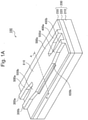
- a perspective view of the 2x2 MMI optical multiplexer/demultiplexer according to present example embodiment is illustrated in Fig. 1A and its sectional view taken along line A-A' of Fig. 1A is illustrated in Fig. 1B .
- Fig. 1A and Fig. 1B A perspective view of the 2x2 MMI optical multiplexer/demultiplexer according to present example embodiment is illustrated in Fig. 1A and its sectional view taken along line A-A' of Fig. 1A is illustrated in Fig. 1B .
- a 2 ⁇ 2 MMI optical multiplexer/demultiplexer 100 includes a SOI substrate (SOI: Semiconductor-on-Insulator) 200, input optical waveguides 300a and 300b, output optical waveguides 400a and 400b, tapered optical waveguides 500a, 500b, 500c, and 500d, and a rib type MMI region 600.
- SOI substrate SOI: Semiconductor-on-Insulator
- the input optical waveguides 300a and 300b, the output optical waveguides 400a and 400b, and the tapered optical waveguides 500a, 500b, 500c, and 500d are simply written as the input optical waveguide 300, the output optical waveguide 400, and the tapered optical waveguide 500 when it is not necessary to particularly distinguish them from another.
- the SOI substrate 200 is a semiconductor slab region and is formed by arranging an insulating film 220 on an upper surface of a substrate 210 and arranging a SOI layer 230 on the surface of the insulating film 220. Then, optical waveguide patterns are exposed to the SOI layer 230 with high precision and a dry etching process is performed, so that the input optical waveguide 300, the output optical waveguide 400, the tapered optical waveguide 500, and the rib type MMI region 600 are formed.
- the input optical waveguides 300a and 300b are straight semiconductor rib regions, are formed in regions of one end side of the SOI layer 230 of the SOI substrate 200, and form single mode optical waveguides of a pair of input sides.
- Optical signals inputted to the input optical waveguides 300a and 300b are inputted to the rib type MMI region 600 via the continuous tapered optical waveguides 500a and 500b.
- the output optical waveguides 400a and 400b are straight semiconductor rib regions, are formed in regions of the other end side of the SOI layer 230 of the SOI substrate 200, and form single mode optical waveguides of a pair of output sides.
- the output optical waveguides 400a and 400b output optical signals, which have been inputted from the rib type MMI region 600 via the continuous tapered optical waveguides 500c and 500d, to connected optical fibers and the like.
- the input optical waveguides 300a and 300b and the output optical waveguides 400a and 400b have the same sectional shapes.
- the tapered optical waveguide 500 smoothly connects the input optical waveguide 300 or the output optical waveguide 400 to the rib type MMI region 600.
- all the four tapered optical waveguides 500a, 500b, 500c, and 500d are formed in a shape with the same length.
- the tapered optical waveguide 500a smoothly connects the input optical waveguide 300a to a MMI part 610 of the rib type MMI region 600
- the tapered optical waveguide 500b smoothly connects the input optical waveguide 300b to the MMI part 610.
- the tapered optical waveguide 500c smoothly connects the output optical waveguide 400a to the MMI part 610 of the rib type MMI region 600
- the tapered optical waveguide 500d smoothly connects the output optical waveguide 400b to the MMI part 610.
- the rib type MMI region 600 includes a semiconductor and allows an optical signal inputted from the input optical waveguide 300a via the tapered optical waveguides 500a to interfere with an optical signal inputted from the input optical waveguide 300b via the tapered optical waveguides 500b. Then, the rib type MMI region 600 outputs the interfered optical signal to the output optical waveguides 400a and 400b via the tapered optical waveguides 500c and 500d.
- thin stepped parts with a finite width are formed at both sidewalls extending in a direction (hereinafter, written as a longitudinal direction) toward the output optical waveguide 400 from the input optical waveguide 300.
- the stepped parts are written as narrow width stepped parts 620a and 620b, and a rib type interference part interposed between the stepped parts 620a and 620b is written as the MMI part 610.
- Widths w of the stepped parts 620a and 620b are formed to be equal to a propagation wavelength and heights h thereof are formed to be equal to a half of the propagation wavelength.
- the widths w and the heights h of the narrow width stepped parts 620a and 620b are as indicated in Fig. 1B .
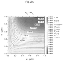
- Fig. 2A and Fig. 2B illustrate a difference n 11 -n 12 (hereinafter, an effective refractive index difference) of a unique value (an effective refractive index n 11 ) of a fundamental mode and a unique value (an effective refractive index n 12 ) of a first high order mode of the rib type MMI region 600 when the sectional shapes of the narrow width stepped parts 620a and 620b are changed in the 2 ⁇ 2 MMI optical multiplexer/demultiplexer 100 configured as above.
- an effective refractive index difference of a unique value (an effective refractive index n 11 ) of a fundamental mode and a unique value (an effective refractive index n 12 ) of a first high order mode of the rib type MMI region 600 when the sectional shapes of the narrow width stepped parts 620a and 620b are changed in the 2 ⁇ 2 MMI optical multiplexer/demultiplexer 100 configured as above.
- the effective refractive index difference is inversely proportional to an interference cycle (a beat length) of the fundamental mode and the first high order mode in the rib type MMI region 600, and is an important parameter for deciding an optimal length of the rib type MMI region 600.
- a subscript of the effective refractive index difference n is written using a sign E of an electric field, but has the same meaning as that of the notation in the present specification.
- Fig. 2A illustrates an effective refractive index difference (n x 11 -n x 12 ) when a main electric field is horizontal to a substrate (an E x mode)
- Fig. 2B illustrates an effective refractive index difference (n y 11 -n y 12 ) when the main electric field is vertical to the substrate (an E y mode).
- a horizontal axis denotes widths w of the narrow width stepped parts 620a and 620b
- a vertical axis denotes heights h of the narrow width stepped parts 620a and 620b
- sections of the narrow width stepped parts 620a and 620b all have the same shape of a rectangle.
- silicon a refractive index 3.48
- SiO 2 a refractive index 1.447
- a signal light wavelength is assumed to 1,550 nm.
- a width of the MMI part 610 is 7 ⁇ m
- a rib height is 0.9 ⁇ m
- a slab thickness is 0.6 ⁇ m.
- an absolute value of the effective refractive index difference is about an amount of 5 ⁇ 10 -3 in the E x mode and the E y mode and corresponds to more than 200 ⁇ m when it is converted to an MMI optimal length for signal light with a wavelength of 1,550 nm.
- the narrow width stepped parts 620a and 620b are not arranged at both sides of the MMI part 610. This state corresponds to the lower left origins (the width w and the height h are all zero) of Fig. 2A and Fig. 2B .
- the effective refractive index difference is constant (that is, a beat length is constant)
- the widths w and the heights h of the narrow width stepped parts 620a and 620b are inversely proportional to each other in the range plotted in Fig. 2A and Fig. 2B . This tendency is common to both the E x mode and the E y mode, but the absolute value itself of the effective refractive index difference slightly deviates between both modes.
- Fig. 3 illustrates a ratio (n x 11 -n x 12 )/(n y 11 -n y 12 ) of the effective refractive index differences of the E x mode and the E y mode.
- the ratio of polarization of the effective refractive index differences monotonically decreases as the widths w and the heights h of the narrow width stepped parts 620a and 620b increase.
- the ratio is 1, the optimal lengths of each polarization in the rib type MMI region 600 coincide with each other, that is, when it is assumed that there is no influence of the input/output optical waveguide, it is probable that it is possible to perform a polarization independent operation of the 2 ⁇ 2 MMI optical multiplexer/demultiplexer.
- the ratio of the effective refractive index differences is about 1.025 in the vicinity of the lower left origin of Fig. 3 , the ratio is 1 when the height h is about 0.5 ⁇ m and the width w is about 1 ⁇ m. This means that it is possible to adjust the polarization dependence of the 2x2 MMI optical multiplexer/demultiplexer 100 within a certain range by adjusting the widths w and the heights h of the narrow width stepped parts 620a and 620b provided at both sides of the MMI part 610.
- the narrow width stepped parts 620a and 620b capable of performing a polarization independent operation.
- the narrow width stepped parts 620a and 620b can be formed by adding one mask, a one-time lithography process, and a one-time etching process of the core layer respectively, an influence to mass productivity and manufacturing yield is also limited.
- the aforementioned discussion corresponds to the case of focusing on only the effective refractive index difference (the beat length) in the rib type MMI region 600 in which the narrow width stepped parts 620a and 620b have been arranged.
- This corresponds to the case in which both the fundamental mode and the first high order mode in the rib type MMI region 600 can be excited with an ideal planar wave.
- a reversible tapered optical waveguide region is arranged between the rib type MMI region 600, and the input optical waveguide 300 and the output optical waveguide 400.
- tapered optical waveguide region a beam shape (mainly, a beam width) continuously changes (the beam with is mainly extended or reduced), and simultaneously an equiphase surface (a wave front) is distorted from a
- tapered optical waveguide region is formed with the tapered optical waveguides 500a, 500b, 500c, and 500d including a semiconductor formed by processing the SOI layer 230 in a strip shape, the reversible tapered optical waveguide region itself has polarization dependence.
- the curvature of the equiphase surface (the wave front) is considered as an amount proportional to a propagation distance, and when the lengths of the tapered optical waveguides 500a, 500b, 500c, and 500d are sufficiently long compared to a wavelength, the signal light shows a behavior approximate to a plane wave.
- the lengths of the tapered optical waveguides 500a, 500b, 500c, and 500d are increased (as the tapered width is gently changed), while the loss (mode conversion loss) due to a mode shape change is suppressed, the loss due to optical absorption or scattering is increased.
- the equiphase surface (the wave front) of an electromagnetic field distribution of signal light to be propagated is kept to be curved.
- signal light is not excited with a plane wave, but is excited in the state in which the equiphase surface (the wave front) has been distorted. This causes finite loss and polarization dependence is shown in the loss itself.
- the extent of contribution of polarization dependence shown by the tapered optical waveguides 500a, 500b, 500c, and 500d is added to the discussion related to the beat length, resulting in a phenomenon actually occurring in the 2 ⁇ 2 MMI optical multiplexer/demultiplexer 100.
- the fact that the 2 ⁇ 2 MMI optical multiplexer/demultiplexer 100 including the tapered optical waveguides 500a, 500b, 500c, and 500d and the rib type MMI region 600 performs a polarization independent operation is separately confirmed through electromagnetic field analysis.
- the heights h and the widths w of the narrow width stepped parts 620a and 620b are substantially inversely proportional to each other. Accordingly, when the areas of the narrow width stepped parts 620a and 620b are equal to each other, it is considered that optical multiplexing and demultiplexing characteristics also show almost the same tendency. However, as the widths w of the narrow width stepped parts 620a and 620b are widened, radiation to a slab region extending outward is promoted, resulting in an increase in insertion loss.
- the widths w of the narrow width stepped parts 620a and 620b are approximately equal to the signal light wavelength of the core material.
- the sectional shapes of the narrow width stepped parts 620a and 620b can also be formed in a right angled triangle for example.
- a rib sidewall is inclined from a surface vertical to the substrate.
- the rib sidewalls of the input optical waveguide 300, the output optical waveguide 400, and the tapered optical waveguide 500 are also inclined.
- the electromagnetic field distributions of the fundamental modes of the input optical waveguide 300 and the output optical waveguide 400 deviate from an assumed shape, so that design of polarization independence becomes difficult. Accordingly, it is practical that the sectional shapes of the narrow width stepped parts 620a and 620b are rectangular.
- the operation of the 2x2 MMI optical multiplexer/demultiplexer 100 described in the first example embodiment will be described.
- the insulating film 220 including a SiO 2 film with a thickness of 3 ⁇ m and the SOI layer 230 serving as a semiconductor layer with a thickness of 1.5 ⁇ m are arranged on the substrate 210, so that the SOI substrate 200 is formed.
- optical waveguide patterns are high precisely formed in the SOI layer 230 on the SOI substrate 200 by using a photolithography technology, so that the 2 ⁇ 2 MMI optical multiplexer/demultiplexer 100 described in the first example embodiment is formed.
- the input optical waveguide 300 and the output optical waveguide 400 are rib type optical waveguides in which Si is used as a core and SiO 2 is used as a clad, and have a rib width of 1.4 ⁇ m, a rib height of 0.9 ⁇ m, and a slab thickness of 0.6 ⁇ m. Furthermore, in a wavelength band of 1,530 nm to 1,610 nm, the input optical waveguide 300 and the output optical waveguide 400 satisfy single mode propagation conditions together with both polarizations of the E x mode and the E y mode.
- the MMI part 610 of the rib type MMI region 600 is formed to have a width of 7 ⁇ m, a length of 234 ⁇ m, a rib height of 0.9 ⁇ m, and a slab thickness of 0.6 ⁇ m. Furthermore, the narrow width stepped parts 620a and 620b are all formed to have a height of 0.2 ⁇ m and a width of 0.5 ⁇ m.
- the aforementioned input optical waveguide 300 and the output optical waveguide 400, and the aforementioned rib type MMI region 600 are smoothly connected to each other by the tapered optical waveguide 500 (a reversible horizontal tapered region) having a length of 50 ⁇ m in which a rib height is 0.9 ⁇ m, a slab thickness is 0.6 ⁇ m, and a width is linearly changed from 1.4 ⁇ m to 3 ⁇ m.
- the tapered optical waveguide 500 a reversible horizontal tapered region having a length of 50 ⁇ m in which a rib height is 0.9 ⁇ m, a slab thickness is 0.6 ⁇ m, and a width is linearly changed from 1.4 ⁇ m to 3 ⁇ m.
- CMOS process such as high precision photolithography using a reduction projection exposure device using ArF in a light source and a phase shift mask, and a low damage dry etching technology.
- a previously stepped SiN film (not illustrated because it is removed in a manufacturing process) is provided as an etching blocking layer to be provided to the surface of the SOI substrate 200, so that the MMI part 610 and the narrow width stepped parts 620a and 620b at both sides thereof are integrally formed with each other in a one-time dry etching process.
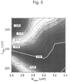
- the transmittance for the E x mode of the 2 ⁇ 2 MMI optical multiplexer/demultiplexer 100 formed as described above is illustrated in Fig. 4
- a ratio (that is, polarization dependence of transmittance) of the transmittance for the E x mode and the transmittance for the E y mode is illustrated in Fig. 5 .
- a horizontal axis denotes the width of a tapered end portion (a wide side being in contact with the MMI part 610) of the tapered optical waveguide 500
- a vertical axis denotes the length of the rib type MMI region 600.
- a signal light wavelength is 1,590 nm.
- the transmittance is defined by Equation 1 below.
- P bar denotes power outputted to a port (a bar output port) of the output optical waveguide 400 in front of signal light with power Pin travelling straight from one side of the input optical waveguide 300
- P cross denotes power outputted to a port (a cross output port) of the output optical waveguide 400 in front of a diagonal line of the MMI part 610.
- the width and the MMI length dependence of a tapered end portion of insertion loss for the E x mode form a track-like contour line group in which a size differs step by step.
- the maximum value (the minimum value of the insertion loss) of the transmittance is -0.04 dB to -0.06 dB (+0.04 dB to +0.06 dB), so that a favorable value can be obtained for a 2x2 optical multiplexer/demultiplexer for a 1.5 ⁇ m band using Si as an optical waveguide core material.
- the transmittance for the E x mode is calculated (not illustrated). From the result, the length of the MMI part 610 of the 2 ⁇ 2 MMI optical multiplexer/demultiplexer 100 is set to 232 ⁇ m and the width of the tapered end portion is set to 3.3 ⁇ m.
- the 2 ⁇ 2 MMI optical multiplexer/demultiplexer 100 designed as described above has practical signal light branching characteristics in the signal light wavelength from 1,570 nm to 1,610 nm in configuring a matrix optical switch even though it is a rib type optical waveguide using the Si core whose section is not a square.
- the E x mode is from 0.08 dB to 0.09 dB
- the E y mode is from 0.07 dB to 0.08 dB
- polarization dependence loss is ⁇ 0.01 dB or less.
- the 2 ⁇ 2 MMI optical multiplexer/demultiplexer 100 including the input/output tapered waveguides it can be understood that it is possible to achieve a structure, in which polarization dependence and wavelength dependence in multiplexing and demultiplexing characteristics are suppressed to a level causing practically no problems over a wide wavelength band, by a practical means by adding required minimum steps.
- the rib type MMI region 600 in which the narrow width stepped parts 620a and 620b are arranged at both sidewalls extending in the longitudinal direction of the MMI part 610, can be arranged in a ROADM (reconfigurable optical add/drop multiplexer), a 90 ° hybrid, an ADM matrix switch and the like, in addition to the MMI optical multiplexer/demultiplexer.
- ROADM reconfigurable optical add/drop multiplexer
- FIG. 6A A perspective view of a 2 ⁇ 2 MMI optical multiplexer/demultiplexer 100B according to the present example embodiment is illustrated in Fig. 6A , and its sectional view taken along line B-B' is illustrated in Fig. 6B .
- narrow width stepped parts 620aB and 620bB are formed in a stair shape by notching corner parts in a rectangular parallelepiped shape while maintaining the areas of the rectangular parallelepiped narrow width stepped parts 620a and 620b described in the example of the first example embodiment.
- each of the narrow width stepped parts 620aB and 620bB according to the present example embodiment, a lower part having a width of 0.4 ⁇ m and a height of 0.2 ⁇ m and an upper part having a width of 0.2 ⁇ m and a height of 0.2 ⁇ m are integrally formed with each other. Except for this point, the narrow width stepped parts 620aB and 620bB are similar to those of the 2x2 MMI optical multiplexer/demultiplexer 100 described in the example of the first example embodiment.
- the 2x2 MMI optical multiplexer/demultiplexer 100B of Fig. 6A and Fig. 6B also obtains practical signal light branching characteristics as a 2 ⁇ 2 optical multiplexer/demultiplexer used in configuring a matrix optical switch even though it is a rib type optical waveguide in which its section is not a square and a Si core is used.
- the E x mode is from 0.08 dB to 0.09 dB
- the E y mode is from 0.07 dB to 0.08 dB
- polarization dependence loss is ⁇ 0.01 dB or less over the signal light wavelength from 1,570 nm to 1,610 nm.
- Si is used as a core material; however, it is possible to expect similar effects even in the case of using dielectric substances other than Si as a core.
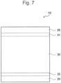
- a rib type optical waveguide 10 can be formed by a substrate 20 and a multi-mode optical interference region 30 formed on the upper surface of the substrate 20 and including a rib type optical waveguide. It is characteristic that both side surfaces of the multi-mode optical interference region 30 are respectively formed in stepped shapes 31 and 32.
- the present invention can be applied to all waveguide optical switches which are used in a M ⁇ N matrix optical switch and the like and include input/output optical waveguides and multi-mode interference regions formed on the same substrate.
Claims (7)
- Multiplexeur/démultiplexeur optique, comprenant :un substrat (210) ;une couche d'isolation (220) ;une couche de noyau semi-conducteur (230) ; etdes guides d'onde optiques à nervures adaptés pour fonctionner sur la bande de longueurs d'onde comprise entre 1530 et 1610 nm, chaque guide d'onde optique nervuré étant formé sur ledit substrat (210) dans ladite couche d'isolation (220) et ladite couche de noyau semi-conducteur (230) ;dans lequel le multiplexeur/démultiplexeur optique comprend en outre quatre desdits guides d'onde optiques nervurés sous la forme de deux guides d'onde optiques d'entrée monomode (300a, 300b) et de deux guides d'onde optiques de sortie monomode (400a, 400b) ; quatre desdits guides d'onde optiques nervurés sous la forme de zones effilées réversibles (500a, 500b, 500c, 500d) comprenant 2x2 guides d'onde qui relient de manière homogène les guides d'onde optiques d'entrée (300a, 300b) et les guides d'onde optiques de sortie (400a, 400b) à un autre desdits guides d'onde optiques nervurés sous la forme d'une zone d'interférence optique multimode (600) ; et la zone d'interférence optique multimode (600) formée sur une surface supérieure du substrat (210),dans lequel chacune des deux surfaces latérales d'un noyau de la zone d'interférence optique multimode (600) forme une partie échelonnée (620a, 620b) ; etdans lequel une hauteur de chaque partie échelonnée (620a, 620b) est approximativement égale à une moitié d'une longueur d'onde de propagation sur la bande de longueurs d'onde ; etdans lequel les guides d'onde optiques d'entrée, les guides d'onde optiques de sortie, la zone d'interférence optique multimode et les zones effilées réversibles sont formés dans la couche de noyau semi-conducteur ; etdans lequel une largeur et la hauteur des parties échelonnées (620a, 620b) sont configurées de sorte qu'une première différence de la zone d'interférence optique multimode (600) et qu'une seconde différence de la zone d'interférence optique multimode (600) soient approximativement égales l'une à l'autre, la première différence étant une différence entre un indice de réfraction effectif d'un mode fondamental et un indice de réfraction effectif d'un premier mode d'ordre élevé lorsqu'une composante de champ électrique principal dans la zone d'interférence optique multimode (600) est horizontale par rapport au substrat (210), la seconde différence étant une différence entre un indice de réfraction effectif du mode fondamental et un indice de réfraction effectif du premier mode d'ordre élevé lorsque la composante de champ électrique principal dans la zone d'interférence optique multimode (600) est perpendiculaire au substrat (210) ; etdans lequel la largeur de chaque partie échelonnée (620a, 620b) est approximativement égale à la longueur d'onde de propagation sur la bande de longueurs d'onde.
- Multiplexeur/démultiplexeur optique selon la revendication 1, dans lequel une transmittance de l'onde lumineuse avec laquelle la composante de champ électrique principal dans la zone d'interférence optique multimode (600) est horizontale par rapport au substrat (210) et une transmittance de l'onde lumineuse avec laquelle la composante de champ électrique principal dans la zone d'interférence optique multimode (600) est perpendiculaire au substrat (210) sont approximativement égales l'une à l'autre.
- Multiplexeur/démultiplexeur optique selon la revendication 1 ou 2, dans lequel, sur la surface supérieure du substrat (210), la couche d'isolation (220) et une couche de semi-conducteur sont disposées, et la couche de noyau semi-conducteur (230) est formée en traitant la couche de semi-conducteur en une forme de bande.
- Multiplexeur/démultiplexeur optique selon l'une quelconque des revendications 1 à 3, dans lequel la partie échelonnée (620aB, 620bB) est formée comme un escalier à deux étages ou plus.
- Multiplexeur/démultiplexeur optique selon l'une quelconque des revendications 1 à 4, dans lequel les guides d'onde optiques d'entrée (300a, 300b) et les guides d'onde optiques de sortie (400a, 400b) comprennent une forme transversale identique.
- Multiplexeur/démultiplexeur optique selon l'une quelconque des revendications 1 à 5, dans lequel les quatre zones effilées réversibles (500a, 500b, 500c, 500d) possèdent la même longueur et la même largeur effilée.
- Multiplexeur/démultiplexeur optique selon la revendication 6, dans lequel la longueur des zones effilées réversibles (500a, 500b, 500c, 500d) est supérieure à la longueur d'onde de propagation.
Applications Claiming Priority (2)
| Application Number | Priority Date | Filing Date | Title |
|---|---|---|---|
| JP2014204120 | 2014-10-02 | ||
| PCT/JP2015/004689 WO2016051698A1 (fr) | 2014-10-02 | 2015-09-15 | Guide d'ondes optique du type à nervure et multiplexeur/démultiplexeur optique l'utilisant |
Publications (3)
| Publication Number | Publication Date |
|---|---|
| EP3203282A1 EP3203282A1 (fr) | 2017-08-09 |
| EP3203282A4 EP3203282A4 (fr) | 2018-06-06 |
| EP3203282B1 true EP3203282B1 (fr) | 2022-01-26 |
Family
ID=55629775
Family Applications (1)
| Application Number | Title | Priority Date | Filing Date |
|---|---|---|---|
| EP15846939.5A Active EP3203282B1 (fr) | 2014-10-02 | 2015-09-15 | Guide d'ondes optique du type à nervure et multiplexeur/démultiplexeur optique l'utilisant |
Country Status (4)
| Country | Link |
|---|---|
| US (1) | US10082623B2 (fr) |
| EP (1) | EP3203282B1 (fr) |
| JP (1) | JP6798313B2 (fr) |
| WO (1) | WO2016051698A1 (fr) |
Families Citing this family (4)
| Publication number | Priority date | Publication date | Assignee | Title |
|---|---|---|---|---|
| JP7480488B2 (ja) * | 2019-10-04 | 2024-05-10 | 富士通オプティカルコンポーネンツ株式会社 | 光半導体素子及び受信器 |
| US10862610B1 (en) | 2019-11-11 | 2020-12-08 | X Development Llc | Multi-channel integrated photonic wavelength demultiplexer |
| US11187854B2 (en) * | 2019-11-15 | 2021-11-30 | X Development Llc | Two-channel integrated photonic wavelength demultiplexer |
| US11360268B1 (en) | 2021-03-17 | 2022-06-14 | Cisco Technology, Inc. | Low-loss and low-crosstalk optical mode multiplexer and optical crossover |
Family Cites Families (14)
| Publication number | Priority date | Publication date | Assignee | Title |
|---|---|---|---|---|
| FR2285623A1 (fr) * | 1974-09-20 | 1976-04-16 | Max Planck Gesellschaft | Dispositif auto-formateur d'images, comportant un guide d'ondes |
| JPH04247408A (ja) | 1991-02-01 | 1992-09-03 | Ibiden Co Ltd | 光導波路 |
| JP2002514783A (ja) | 1998-05-08 | 2002-05-21 | ザ トラスティーズ オブ コロンビア ユニヴァーシティ イン ザ シティ オブ ニューヨーク | 小型にした干渉に基づくマルチモードカップラ |
| JP2001183710A (ja) | 1999-12-27 | 2001-07-06 | Kddi Corp | 多モード干渉導波路型光スイッチ |
| US6856732B2 (en) * | 2001-06-13 | 2005-02-15 | Intel Corporation | Method and apparatus for adding/droping optical signals in a semiconductor substrate |
| FI20020698A0 (fi) * | 2002-04-11 | 2002-04-11 | Valtion Teknillinen | Integroidun optisen piirin valokanava ja menetelmä valokanavan valmistamiseksi |
| SE528653C2 (sv) * | 2005-05-30 | 2007-01-09 | Phoxtal Comm Ab | Integrerat chip |
| US7116880B1 (en) * | 2005-06-30 | 2006-10-03 | Xerox Corporation | Decreased crosstalk in adjacent photonic waveguides |
| US7184207B1 (en) * | 2005-09-27 | 2007-02-27 | Bookham Technology Plc | Semiconductor optical device |
| GB2438222A (en) * | 2006-05-17 | 2007-11-21 | Bookham Technology Plc | Multimode interference waveguide coupler |
| JP5120330B2 (ja) | 2009-04-27 | 2013-01-16 | 三菱電機株式会社 | 半導体光素子とその製造方法 |
| WO2011019887A2 (fr) * | 2009-08-14 | 2011-02-17 | Massachusetts Institute Of Technology | Coupleur de guides dondes présentant un amincissement tridimensionnel continu |
| JP5413865B1 (ja) * | 2012-12-27 | 2014-02-12 | 株式会社フジクラ | 光導波路素子及び光変調器 |
| CN204302526U (zh) | 2014-12-26 | 2015-04-29 | 江苏尚飞光电科技有限公司 | 偏振分束旋转器 |
-
2015
- 2015-09-15 EP EP15846939.5A patent/EP3203282B1/fr active Active
- 2015-09-15 JP JP2016551505A patent/JP6798313B2/ja active Active
- 2015-09-15 US US15/514,563 patent/US10082623B2/en active Active
- 2015-09-15 WO PCT/JP2015/004689 patent/WO2016051698A1/fr active Application Filing
Non-Patent Citations (1)
| Title |
|---|
| None * |
Also Published As
| Publication number | Publication date |
|---|---|
| US10082623B2 (en) | 2018-09-25 |
| JPWO2016051698A1 (ja) | 2017-07-13 |
| US20170227712A1 (en) | 2017-08-10 |
| EP3203282A4 (fr) | 2018-06-06 |
| WO2016051698A1 (fr) | 2016-04-07 |
| JP6798313B2 (ja) | 2020-12-09 |
| EP3203282A1 (fr) | 2017-08-09 |
Similar Documents
| Publication | Publication Date | Title |
|---|---|---|
| EP3111263B1 (fr) | Appareil et procédé pour polariseur de guide d'ondes comprenant une série de coudes | |
| EP1226461B1 (fr) | Phasar a bandes passantes aplaties | |
| US6212315B1 (en) | Channel power equalizer for a wavelength division multiplexed system | |
| JP5263045B2 (ja) | 偏波無依存型光装置 | |
| WO2002088791A2 (fr) | Appareil optique et procede ayant une dispersion de vitesse de groupe predeterminee | |
| JP2007072433A (ja) | 光集積素子及び光制御素子 | |
| EP3203282B1 (fr) | Guide d'ondes optique du type à nervure et multiplexeur/démultiplexeur optique l'utilisant | |
| JP2005010805A (ja) | 導波路型光干渉計 | |
| CN113777708B (zh) | 模变换器 | |
| JP6666423B2 (ja) | 高インデックスコントラストのフォトニックデバイスおよびその応用 | |
| Brunetti et al. | Design of a large bandwidth 2× 2 interferometric switching cell based on a sub-wavelength grating | |
| CN110573918A (zh) | T形阵列式波导光栅 | |
| JP2014041252A (ja) | 光導波路素子 | |
| JP2011039383A (ja) | 偏波無依存型光波長フィルタ、光合分波素子及びマッハツェンダ干渉器 | |
| WO2014030576A1 (fr) | Élément à guides d'ondes optiques | |
| JP4477260B2 (ja) | 導波路型光カプラおよび該導波路型光カプラを用いた光合分波器 | |
| Hammood et al. | Four-channel, silicon photonic, wavelength multiplexer-demultiplexer with high channel isolations | |
| CN117043650A (zh) | 低损耗、低串扰光模式多路复用器和光学交叉互连件 | |
| US20040228574A1 (en) | Switchable optical dispersion compensator using Bragg-grating | |
| JP4776082B2 (ja) | 平面光導波路型マッハツェンダー回路および該平面光導波路型マッハツェンダー回路を用いた平面光導波回路ならびに光合分波器 | |
| Truong et al. | A design of triplexer based on a 2× 2 butterfly MMI coupler and a directional coupler using silicon waveguides | |
| US20190056551A1 (en) | Broadband star coupler | |
| Juhari et al. | Optical loss analysis in 13-channel SOI-based AWG for CWDM network | |
| JP2010262314A (ja) | 平面光導波回路およびそれを用いた光合分波器 | |
| JP2013041146A (ja) | 波長選択性多モード干渉導波路デバイス |
Legal Events
| Date | Code | Title | Description |
|---|---|---|---|
| STAA | Information on the status of an ep patent application or granted ep patent |
Free format text: STATUS: THE INTERNATIONAL PUBLICATION HAS BEEN MADE |
|
| PUAI | Public reference made under article 153(3) epc to a published international application that has entered the european phase |
Free format text: ORIGINAL CODE: 0009012 |
|
| STAA | Information on the status of an ep patent application or granted ep patent |
Free format text: STATUS: REQUEST FOR EXAMINATION WAS MADE |
|
| 17P | Request for examination filed |
Effective date: 20170502 |
|
| AK | Designated contracting states |
Kind code of ref document: A1 Designated state(s): AL AT BE BG CH CY CZ DE DK EE ES FI FR GB GR HR HU IE IS IT LI LT LU LV MC MK MT NL NO PL PT RO RS SE SI SK SM TR |
|
| AX | Request for extension of the european patent |
Extension state: BA ME |
|
| DAV | Request for validation of the european patent (deleted) | ||
| DAX | Request for extension of the european patent (deleted) | ||
| A4 | Supplementary search report drawn up and despatched |
Effective date: 20180507 |
|
| RIC1 | Information provided on ipc code assigned before grant |
Ipc: G02B 6/125 20060101ALI20180430BHEP Ipc: G02B 6/293 20060101ALI20180430BHEP Ipc: G02B 6/28 20060101ALI20180430BHEP Ipc: G02B 6/12 20060101ALN20180430BHEP Ipc: G02B 6/122 20060101AFI20180430BHEP |
|
| STAA | Information on the status of an ep patent application or granted ep patent |
Free format text: STATUS: EXAMINATION IS IN PROGRESS |
|
| 17Q | First examination report despatched |
Effective date: 20200220 |
|
| STAA | Information on the status of an ep patent application or granted ep patent |
Free format text: STATUS: EXAMINATION IS IN PROGRESS |
|
| RIC1 | Information provided on ipc code assigned before grant |
Ipc: G02B 6/12 20060101ALN20210604BHEP Ipc: G02B 6/293 20060101ALI20210604BHEP Ipc: G02B 6/28 20060101ALI20210604BHEP Ipc: G02B 6/125 20060101ALI20210604BHEP Ipc: G02B 6/122 20060101AFI20210604BHEP |
|
| RIC1 | Information provided on ipc code assigned before grant |
Ipc: G02B 6/12 20060101ALN20210611BHEP Ipc: G02B 6/293 20060101ALI20210611BHEP Ipc: G02B 6/28 20060101ALI20210611BHEP Ipc: G02B 6/125 20060101ALI20210611BHEP Ipc: G02B 6/122 20060101AFI20210611BHEP |
|
| RIC1 | Information provided on ipc code assigned before grant |
Ipc: G02B 6/12 20060101ALN20210721BHEP Ipc: G02B 6/293 20060101ALI20210721BHEP Ipc: G02B 6/28 20060101ALI20210721BHEP Ipc: G02B 6/125 20060101ALI20210721BHEP Ipc: G02B 6/122 20060101AFI20210721BHEP |
|
| GRAP | Despatch of communication of intention to grant a patent |
Free format text: ORIGINAL CODE: EPIDOSNIGR1 |
|
| STAA | Information on the status of an ep patent application or granted ep patent |
Free format text: STATUS: GRANT OF PATENT IS INTENDED |
|
| RIC1 | Information provided on ipc code assigned before grant |
Ipc: G02B 6/12 20060101ALN20210820BHEP Ipc: G02B 6/293 20060101ALI20210820BHEP Ipc: G02B 6/28 20060101ALI20210820BHEP Ipc: G02B 6/125 20060101ALI20210820BHEP Ipc: G02B 6/122 20060101AFI20210820BHEP |
|
| INTG | Intention to grant announced |
Effective date: 20210915 |
|
| GRAS | Grant fee paid |
Free format text: ORIGINAL CODE: EPIDOSNIGR3 |
|
| GRAA | (expected) grant |
Free format text: ORIGINAL CODE: 0009210 |
|
| STAA | Information on the status of an ep patent application or granted ep patent |
Free format text: STATUS: THE PATENT HAS BEEN GRANTED |
|
| AK | Designated contracting states |
Kind code of ref document: B1 Designated state(s): AL AT BE BG CH CY CZ DE DK EE ES FI FR GB GR HR HU IE IS IT LI LT LU LV MC MK MT NL NO PL PT RO RS SE SI SK SM TR |
|
| REG | Reference to a national code |
Ref country code: GB Ref legal event code: FG4D |
|
| REG | Reference to a national code |
Ref country code: CH Ref legal event code: EP |
|
| REG | Reference to a national code |
Ref country code: AT Ref legal event code: REF Ref document number: 1465723 Country of ref document: AT Kind code of ref document: T Effective date: 20220215 |
|
| REG | Reference to a national code |
Ref country code: IE Ref legal event code: FG4D |
|
| REG | Reference to a national code |
Ref country code: DE Ref legal event code: R096 Ref document number: 602015076709 Country of ref document: DE |
|
| REG | Reference to a national code |
Ref country code: LT Ref legal event code: MG9D |
|
| REG | Reference to a national code |
Ref country code: NL Ref legal event code: MP Effective date: 20220126 |
|
| REG | Reference to a national code |
Ref country code: AT Ref legal event code: MK05 Ref document number: 1465723 Country of ref document: AT Kind code of ref document: T Effective date: 20220126 |
|
| PG25 | Lapsed in a contracting state [announced via postgrant information from national office to epo] |
Ref country code: NL Free format text: LAPSE BECAUSE OF FAILURE TO SUBMIT A TRANSLATION OF THE DESCRIPTION OR TO PAY THE FEE WITHIN THE PRESCRIBED TIME-LIMIT Effective date: 20220126 |
|
| PG25 | Lapsed in a contracting state [announced via postgrant information from national office to epo] |
Ref country code: SE Free format text: LAPSE BECAUSE OF FAILURE TO SUBMIT A TRANSLATION OF THE DESCRIPTION OR TO PAY THE FEE WITHIN THE PRESCRIBED TIME-LIMIT Effective date: 20220126 Ref country code: RS Free format text: LAPSE BECAUSE OF FAILURE TO SUBMIT A TRANSLATION OF THE DESCRIPTION OR TO PAY THE FEE WITHIN THE PRESCRIBED TIME-LIMIT Effective date: 20220126 Ref country code: PT Free format text: LAPSE BECAUSE OF FAILURE TO SUBMIT A TRANSLATION OF THE DESCRIPTION OR TO PAY THE FEE WITHIN THE PRESCRIBED TIME-LIMIT Effective date: 20220526 Ref country code: NO Free format text: LAPSE BECAUSE OF FAILURE TO SUBMIT A TRANSLATION OF THE DESCRIPTION OR TO PAY THE FEE WITHIN THE PRESCRIBED TIME-LIMIT Effective date: 20220426 Ref country code: LT Free format text: LAPSE BECAUSE OF FAILURE TO SUBMIT A TRANSLATION OF THE DESCRIPTION OR TO PAY THE FEE WITHIN THE PRESCRIBED TIME-LIMIT Effective date: 20220126 Ref country code: HR Free format text: LAPSE BECAUSE OF FAILURE TO SUBMIT A TRANSLATION OF THE DESCRIPTION OR TO PAY THE FEE WITHIN THE PRESCRIBED TIME-LIMIT Effective date: 20220126 Ref country code: ES Free format text: LAPSE BECAUSE OF FAILURE TO SUBMIT A TRANSLATION OF THE DESCRIPTION OR TO PAY THE FEE WITHIN THE PRESCRIBED TIME-LIMIT Effective date: 20220126 Ref country code: BG Free format text: LAPSE BECAUSE OF FAILURE TO SUBMIT A TRANSLATION OF THE DESCRIPTION OR TO PAY THE FEE WITHIN THE PRESCRIBED TIME-LIMIT Effective date: 20220426 |
|
| PG25 | Lapsed in a contracting state [announced via postgrant information from national office to epo] |
Ref country code: PL Free format text: LAPSE BECAUSE OF FAILURE TO SUBMIT A TRANSLATION OF THE DESCRIPTION OR TO PAY THE FEE WITHIN THE PRESCRIBED TIME-LIMIT Effective date: 20220126 Ref country code: LV Free format text: LAPSE BECAUSE OF FAILURE TO SUBMIT A TRANSLATION OF THE DESCRIPTION OR TO PAY THE FEE WITHIN THE PRESCRIBED TIME-LIMIT Effective date: 20220126 Ref country code: GR Free format text: LAPSE BECAUSE OF FAILURE TO SUBMIT A TRANSLATION OF THE DESCRIPTION OR TO PAY THE FEE WITHIN THE PRESCRIBED TIME-LIMIT Effective date: 20220427 Ref country code: FI Free format text: LAPSE BECAUSE OF FAILURE TO SUBMIT A TRANSLATION OF THE DESCRIPTION OR TO PAY THE FEE WITHIN THE PRESCRIBED TIME-LIMIT Effective date: 20220126 Ref country code: AT Free format text: LAPSE BECAUSE OF FAILURE TO SUBMIT A TRANSLATION OF THE DESCRIPTION OR TO PAY THE FEE WITHIN THE PRESCRIBED TIME-LIMIT Effective date: 20220126 |
|
| PG25 | Lapsed in a contracting state [announced via postgrant information from national office to epo] |
Ref country code: IS Free format text: LAPSE BECAUSE OF FAILURE TO SUBMIT A TRANSLATION OF THE DESCRIPTION OR TO PAY THE FEE WITHIN THE PRESCRIBED TIME-LIMIT Effective date: 20220526 |
|
| REG | Reference to a national code |
Ref country code: DE Ref legal event code: R097 Ref document number: 602015076709 Country of ref document: DE |
|
| PG25 | Lapsed in a contracting state [announced via postgrant information from national office to epo] |
Ref country code: SM Free format text: LAPSE BECAUSE OF FAILURE TO SUBMIT A TRANSLATION OF THE DESCRIPTION OR TO PAY THE FEE WITHIN THE PRESCRIBED TIME-LIMIT Effective date: 20220126 Ref country code: SK Free format text: LAPSE BECAUSE OF FAILURE TO SUBMIT A TRANSLATION OF THE DESCRIPTION OR TO PAY THE FEE WITHIN THE PRESCRIBED TIME-LIMIT Effective date: 20220126 Ref country code: RO Free format text: LAPSE BECAUSE OF FAILURE TO SUBMIT A TRANSLATION OF THE DESCRIPTION OR TO PAY THE FEE WITHIN THE PRESCRIBED TIME-LIMIT Effective date: 20220126 Ref country code: EE Free format text: LAPSE BECAUSE OF FAILURE TO SUBMIT A TRANSLATION OF THE DESCRIPTION OR TO PAY THE FEE WITHIN THE PRESCRIBED TIME-LIMIT Effective date: 20220126 Ref country code: DK Free format text: LAPSE BECAUSE OF FAILURE TO SUBMIT A TRANSLATION OF THE DESCRIPTION OR TO PAY THE FEE WITHIN THE PRESCRIBED TIME-LIMIT Effective date: 20220126 Ref country code: CZ Free format text: LAPSE BECAUSE OF FAILURE TO SUBMIT A TRANSLATION OF THE DESCRIPTION OR TO PAY THE FEE WITHIN THE PRESCRIBED TIME-LIMIT Effective date: 20220126 |
|
| PG25 | Lapsed in a contracting state [announced via postgrant information from national office to epo] |
Ref country code: AL Free format text: LAPSE BECAUSE OF FAILURE TO SUBMIT A TRANSLATION OF THE DESCRIPTION OR TO PAY THE FEE WITHIN THE PRESCRIBED TIME-LIMIT Effective date: 20220126 |
|
| PLBE | No opposition filed within time limit |
Free format text: ORIGINAL CODE: 0009261 |
|
| STAA | Information on the status of an ep patent application or granted ep patent |
Free format text: STATUS: NO OPPOSITION FILED WITHIN TIME LIMIT |
|
| 26N | No opposition filed |
Effective date: 20221027 |
|
| PG25 | Lapsed in a contracting state [announced via postgrant information from national office to epo] |
Ref country code: SI Free format text: LAPSE BECAUSE OF FAILURE TO SUBMIT A TRANSLATION OF THE DESCRIPTION OR TO PAY THE FEE WITHIN THE PRESCRIBED TIME-LIMIT Effective date: 20220126 |
|
| REG | Reference to a national code |
Ref country code: DE Ref legal event code: R119 Ref document number: 602015076709 Country of ref document: DE |
|
| PG25 | Lapsed in a contracting state [announced via postgrant information from national office to epo] |
Ref country code: MC Free format text: LAPSE BECAUSE OF FAILURE TO SUBMIT A TRANSLATION OF THE DESCRIPTION OR TO PAY THE FEE WITHIN THE PRESCRIBED TIME-LIMIT Effective date: 20220126 |
|
| REG | Reference to a national code |
Ref country code: CH Ref legal event code: PL |
|
| REG | Reference to a national code |
Ref country code: BE Ref legal event code: MM Effective date: 20220930 |
|
| PG25 | Lapsed in a contracting state [announced via postgrant information from national office to epo] |
Ref country code: LU Free format text: LAPSE BECAUSE OF NON-PAYMENT OF DUE FEES Effective date: 20220915 |
|
| PG25 | Lapsed in a contracting state [announced via postgrant information from national office to epo] |
Ref country code: LI Free format text: LAPSE BECAUSE OF NON-PAYMENT OF DUE FEES Effective date: 20220930 Ref country code: IT Free format text: LAPSE BECAUSE OF FAILURE TO SUBMIT A TRANSLATION OF THE DESCRIPTION OR TO PAY THE FEE WITHIN THE PRESCRIBED TIME-LIMIT Effective date: 20220126 Ref country code: IE Free format text: LAPSE BECAUSE OF NON-PAYMENT OF DUE FEES Effective date: 20220915 Ref country code: FR Free format text: LAPSE BECAUSE OF NON-PAYMENT OF DUE FEES Effective date: 20220930 Ref country code: DE Free format text: LAPSE BECAUSE OF NON-PAYMENT OF DUE FEES Effective date: 20230401 Ref country code: CH Free format text: LAPSE BECAUSE OF NON-PAYMENT OF DUE FEES Effective date: 20220930 |
|
| PG25 | Lapsed in a contracting state [announced via postgrant information from national office to epo] |
Ref country code: BE Free format text: LAPSE BECAUSE OF NON-PAYMENT OF DUE FEES Effective date: 20220930 |
|
| PGFP | Annual fee paid to national office [announced via postgrant information from national office to epo] |
Ref country code: GB Payment date: 20230920 Year of fee payment: 9 |
|
| PG25 | Lapsed in a contracting state [announced via postgrant information from national office to epo] |
Ref country code: HU Free format text: LAPSE BECAUSE OF FAILURE TO SUBMIT A TRANSLATION OF THE DESCRIPTION OR TO PAY THE FEE WITHIN THE PRESCRIBED TIME-LIMIT; INVALID AB INITIO Effective date: 20150915 |
|
| PG25 | Lapsed in a contracting state [announced via postgrant information from national office to epo] |
Ref country code: CY Free format text: LAPSE BECAUSE OF FAILURE TO SUBMIT A TRANSLATION OF THE DESCRIPTION OR TO PAY THE FEE WITHIN THE PRESCRIBED TIME-LIMIT Effective date: 20220126 |