EP3201929B1 - Nail lamp - Google Patents
Nail lamp Download PDFInfo
- Publication number
- EP3201929B1 EP3201929B1 EP15846788.6A EP15846788A EP3201929B1 EP 3201929 B1 EP3201929 B1 EP 3201929B1 EP 15846788 A EP15846788 A EP 15846788A EP 3201929 B1 EP3201929 B1 EP 3201929B1
- Authority
- EP
- European Patent Office
- Prior art keywords
- intensity
- light
- nail
- light source
- reflector
- Prior art date
- Legal status (The legal status is an assumption and is not a legal conclusion. Google has not performed a legal analysis and makes no representation as to the accuracy of the status listed.)
- Active
Links
Images


Classifications
-
- A—HUMAN NECESSITIES
- A45—HAND OR TRAVELLING ARTICLES
- A45D—HAIRDRESSING OR SHAVING EQUIPMENT; EQUIPMENT FOR COSMETICS OR COSMETIC TREATMENTS, e.g. FOR MANICURING OR PEDICURING
- A45D29/00—Manicuring or pedicuring implements
- A45D29/22—Finger-supports
-
- F—MECHANICAL ENGINEERING; LIGHTING; HEATING; WEAPONS; BLASTING
- F26—DRYING
- F26B—DRYING SOLID MATERIALS OR OBJECTS BY REMOVING LIQUID THEREFROM
- F26B9/00—Machines or apparatus for drying solid materials or objects at rest or with only local agitation; Domestic airing cupboards
- F26B9/003—Small self-contained devices, e.g. portable
-
- A—HUMAN NECESSITIES
- A45—HAND OR TRAVELLING ARTICLES
- A45D—HAIRDRESSING OR SHAVING EQUIPMENT; EQUIPMENT FOR COSMETICS OR COSMETIC TREATMENTS, e.g. FOR MANICURING OR PEDICURING
- A45D29/00—Manicuring or pedicuring implements
-
- F—MECHANICAL ENGINEERING; LIGHTING; HEATING; WEAPONS; BLASTING
- F26—DRYING
- F26B—DRYING SOLID MATERIALS OR OBJECTS BY REMOVING LIQUID THEREFROM
- F26B3/00—Drying solid materials or objects by processes involving the application of heat
- F26B3/28—Drying solid materials or objects by processes involving the application of heat by radiation, e.g. from the sun
-
- A—HUMAN NECESSITIES
- A45—HAND OR TRAVELLING ARTICLES
- A45D—HAIRDRESSING OR SHAVING EQUIPMENT; EQUIPMENT FOR COSMETICS OR COSMETIC TREATMENTS, e.g. FOR MANICURING OR PEDICURING
- A45D2200/00—Details not otherwise provided for in A45D
- A45D2200/20—Additional enhancing means
- A45D2200/205—Radiation, e.g. UV, infrared
Definitions
- the present invention is related to a light-curing nail lamp, which has a light source designed to cure a light-curable nail product on a user's nails.
- nail polishes e.g., lacquers, varnish or enamels
- artificial nails e.g., gels or acrylics
- nail polishes typically comprise various solid components, which are dissolved and/or suspended in non-reactive solvents. Upon application and drying, the solids deposit on the nail surface as a clear, translucent, or colored film.
- nail polishes are easily scratched and are easily removable with solvent, usually within one minute and if not removed as described, will chip or peel from the natural nail in one to five days.
- Conventional artificial nails are comprised of chemically reactive monomers, and/or oligomers, and photoinitiators in combination with non-reactive polymers to create systems that are typically 100% solids and do not require non-reactive solvents.
- the photoinitiators respond differently depending on a light source's intensity and wavelength.
- the photoinitiators react with light to form radical photoinitiators, which in turn, react with the ingredients listed above to form a nail coating.
- a mixture with more photoinitiators requires a lower intensity to properly cure the mixture, while a mixture with more colorant(s), which block light from penetrating through the coating, requires a higher intensity to properly cure the mixture.
- higher wavelengths of emitted light are better for bulk curing, while lower wavelengths of emitted light are better for surface curing.
- a light curable nail product e.g., gel or acrylic
- a user's nails e.g., finger nails, toe nails
- the nail lamp emits light that emits the light-curable nail product, providing a durable nail product.
- US 2013/0255100 discloses a nail lamp having the features of the preamble of claim 1.
- the present invention provides a nail lamp with improved light-curing characteristics (e.g., faster curing times, more consistent curing at a single nail and/or across a plurality of nails on a user's appendage), improved bulb positioning, an open architecture that permits the user's hands/feet to remain substantially visible and exposed to the an1bient environment, a compact stowable size, reduced power consumption, and/or reduced heat generation.
- improved light-curing characteristics e.g., faster curing times, more consistent curing at a single nail and/or across a plurality of nails on a user's appendage
- improved bulb positioning e.g., an open architecture that permits the user's hands/feet to remain substantially visible and exposed to the an1bient environment, a compact stowable size, reduced power consumption, and/or reduced heat generation.
- the present invention provides a portable, easily carried nail lamp.
- the present invention provides a nail lamp that focuses curing light on the user's nails while limiting the user's skin exposure to such light.
- the invention is as defined in claims 1 to 8.
- One or more embodiments provide a reflector connected to a top surface of the base of the nail lamp.
- the reflector is arranged in an arc-shape between a left portion of the base and the right portion of the base.
- the reflector may include a wall portion and a base portion, in which the wall portion may be substantially perpendicular to the base portion or may be at an angle exceeding 90° relative to the base portion.
- One or more embodiments provide source reflectors arranged within the support around each of the light sources.
- the source reflector has a small end and a large end, and each of these ends may have an opening shaped as an oval, a circle, a square, a rectangle, or any other shape.
- the source reflector(s) is structured to direct light from the light source(s) onto a corresponding nail within the space.
- the each light source(s) is a multiple-wavelength LED device.
- the LED device is a circuit board with a plurality of semiconductor chips coupled thereto, and may include a protective lens to cover the circuit board. These chips may be of the same wavelength or may be of different wavelengths.
- the LED device may be pulsed.
- the LED may be pulsed between an off state and a peak intensity on state, between an off state and an intermediate intensity on state, between an intermediate intensity on state and a peak intensity on state, or between two intermediate intensities at an on state.
- the pulsing may be performed according to pulsing sequences of varying intensities and varying time durations.
- One or more embodiments provide a controller that may control the intensity of the LED device and/or control the pulsing sequence of the LED device.
- the controller may include a controller interface connected to control buttons, a control dial, a digital input pad, and the like, located on the nail lamp.
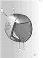
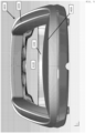
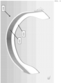
- FIGS. 1-8 illustrate a nail lamp 6010 according to the present invention.
- the lamp 6010 includes a base 6020, a support 6030, a light source 6050, and a reflector 6260.
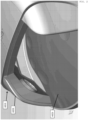
- the support 6030 of the lamp 6010 is connected to the base 6020 such that the support 6030 is in its operative position and a space 6110 between the base 6020 and the support 6030 is sized to accommodate a user's appendage.
- the space 6110 is open to an ambient environment at a rear portion 6110a of the space 6110.
- the space 6110 may additionally be open to the ambient environment at a front, a left, and/or a right portion of the space 6110.
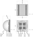
- the base 6020 may be flat or may have a convex shape, as depicted in FIGS. 5 and 8 .
- a light source 6050 is disposed within the support 6030 of the lamp 6010.
- the light source 6050 is configured to produce light to cure a light-curable nail product, and the light source 6050 is positioned to direct the light onto a nail of the user's appendage.
- the light source 6050 includes a plurality of lighting elements.
- the light source 50 includes multiple LED devices.
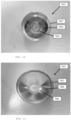
- FIG. 3 shows a source reflector 6055 arranged within the support 6030 around the light source 6050.
- a plurality of light sources 6050 is arranged in the support 6030.
- the lamp 6010 may include two, three, four, or more light sources 6050.
- a light source 6050 corresponding to each of five nails of the user's appendage is shown.
- each of the plurality of light sources 6050 may includes multiple LED devices.
- the lamp 6010 may be configured to receive five nails of any of the user's hands and feet.
- the lamp 6010 may include a light source 6050 corresponding to each nail of a left appendage or a right appendage of the user.
- the lamp 6010 may include a total of seven (7) light sources 6050: one light source for each of the user's left and right thumb nails and left and right pinky finger nails, a common light source for the user's left ring finger nail and the user's right index finger nail, a common light source for the user's left and right middle finger nails, and a common light source for the user's left index finger nail and the user's right ring finger nail for example.
- the lamp 6010 may be configured to accept two appendages.
- ten (10) light sources 6050 may be included, one for each nail, where each light source 6050 corresponds to an individual nail of each finger/toe of the user.
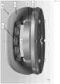
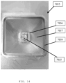
- the lamp 6010 includes a reflector 6260 connected to a top surface of the base 6020.
- the reflector 6260 is arranged in an arc-shape between a left portion 6020a of the base 6020 and a right portion 6020b of the base 6020. Such an arrangement allows the reflector 6260 to reflect the light produced by the light source(s) 6050 to a front edge portion of the user's nail(s) as well as an underneath portion of the nail(s).
- the reflector 6260 may be arranged in a position that is offset from a perimeter of the base 6020, as shown in FIG. 7 , or alternatively, may be arranged at the perimeter of the base 6020 (not shown).
- the reflector 6260 may be made of a plastic material, a metallic material, and/or any other type of suitably rigid material.
- the reflector 6260 may be made of a plastic material and coated with a metallic layer having a polished finished to enhance its reflectivity.
- the reflector 6260 may include a wall portion 6262 and optionally a base portion 6264, as shown in FIGS. 6 and 7 .
- the base portion 6264 enhances curing of the nail product at the underneath portion of the nail(s).
- the wall portion 6262 may be substantially perpendicular (i.e., at 90°) to the base portion 6264, or alternatively, may be at an angle a smaller or larger than 90° relative to the base portion 6264.
- the wall portion 6262 is inclined at an angle of about 90° to 100° relative to a surface of the base portion 6264, such that a top edge of the wall portion is inclined away from a central region 6020c of the base 6020, as shown in FIG. 8 .
- the wall portion 6262 may, in another embodiment, be at an angle of about 85°-90° relative to a surface of the base portion 6264 such that a top edge of the wall portion is inclined towards a central region 6020c of the base 6020.
- the angle may be approximately 93° relative to the surface of the base portion 6264. Optimization of the angle of inclination ⁇ may be achieved by varying a height of the wall portion 6262, a width of the base portion 6264, and/or a distance of the wall portion 6262 from the nail(s). In an embodiment, the height of the wall portion 6262 is taller than a height of the user's finger(s)/toe(s). For example, the reflector 6260 is positioned approximately 16 mm from an edge of the nail(s) and has an approximate height of 18 mm.
- the base 6020 may include position indicators 6095 a , 6095 b , 6095 c , 6095 d , 6095 e , 6095 f , 6095 g (collectively "position indicators 6095").
- the position indicators 6095 may be represented by an indentation, a protrusion, a marking, and/or any other type of suitable means to indicate a desired nail position.
- Each position indicator 6095 corresponds to a nail of a right appendage and/or a nail of a left appendage.
- Position indicators 6095 a , 6095 b , 6095 c , 6095 d , 6095 e correspond to a thumb, index, middle, ring, and pinky finger of the user's right hand, respectively, for example.
- Position indicators 6095 f , 6095 d , 6095 c , 6095 b , 6095 g correspond to a thumb, index, middle, ring, and pinky finger of the user's left hand, respectively, for example.
- the descriptions herein will refer to nails on the user's hands.
- the position indicators could also be analogously arranged for toes on the user's foot/feet.
- central ones of the position indicators 6095 b , 6095 c , 6095 d are common for both the left and right hands (i.e ., the three central nails of the left and right hands).
- the right-most position indicator for the right hand 6095e is positioned closer to a front portion of the base 6020 the right-most position indicator for the left hand 6095 f .
- the left-most position indicator for the left hand 6095 g is positioned closer to the front portion of the base than the left-most position indicator for the right hand 6095 a .
- the base portion 6264 of the reflector 6260 may be a uniform width from the left side of the base 6264 to the right side of the base 6264.
- the base portion 6264 of the reflector 6260 may be wider at its ends (i.e., at a position approximate position indicators 6095 a , 6095 f and may be narrower in a central region (i.e., at a position approximate position indictors 6095 b , 6095 c , 6095 d ).
- the wider base portion 6264 provides more efficient and uniform curing of the left and right thumb nails positioned at position indicators 6095a, 6095f.
- FIGS. 10-15 illustrate a nail lamp 7010 and associated components according to another aspect of the present invention. To avoid redundant descriptions, components of the lamp 7010 that are similar to components of the lamp 6010 are identified using comparable reference numbers in the 7000 range
- the lamp 7010 is similar to the lamp 6010, except the lamp 7010 does not include a reflector such as the reflector 6260. Additionally, the lamp 7010 includes a source reflector 7055.
- the lamp 7010 includes a base 7020, a support 7030, a light source 7050, and a source reflector 7055.
- the source reflector 7055 is arranged within the support 7030 around the light source 7050.
- the source reflector 7055 may be made of a plastic material, a metallic material, and/or any other type of suitably rigid material.
- the source reflector 7055 may be made of a plastic material and coated with a metallic layer having a polished finished to enhance reflectivity.
- the source reflector 7055 is structured to direct the light from the light source 7050 onto a corresponding nail within a space 7110 between the base 7020 and the support 7030.
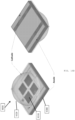
- the source reflector 7055 may be designed as a frustum reflector, with a small end 7056 and a large end 7057, as shown in FIG. 13 .
- Each of the small end 7056 and large end 7057 of the source reflector 7055 may have openings shaped as one of (i) an oval, (ii) a circle, (iii) a square, (iv) a rectangle, (v) an ellipse, and (vi) a polygon. Other shapes may also be used for the openings.
- FIG. 11 shows a source reflector 7055 with circular openings, FIGS.
- FIGS. 9-14 show a source reflector 7055 with oval openings
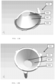
- FIG. 15 shows a source reflector 7055 with rectangular openings. While FIG. 15 is the only illustration depicting the light source 7050 in conjunction with the source reflector 7055, it should be understood that the light source 7050 is similarly arranged in FIGS. 9-14 .
- a wall 7058 of the source reflector 7055 may be inclined at an angle ⁇ between about 20° and about 50° relative to a vertical position from the small end of the source reflector 7055.
- the wall 7058 is inclined at an angle ⁇ of approximately 35° relative to the vertical position, and the source reflector 7055 has a vertical height of 11 mm.
- This arrangement focuses the light from the light source 7050 and directs the light to a corresponding nail within the space 7110. It should be understood that optimal values for the height of the source reflector 7055, the shape of the reflector openings, and the angle of inclination ⁇ are based on the dimensions of the light source 7050, a light disbursement angle of the light source 7050, and distance from the nail(s).
- the source reflector 7055 has an opening at the small end 7056 shaped as an oval and an opening at the large end 7057 shaped as an oval.
- the small end 7056 has a minor axis measuring approximately 7.5 mm and a major axis measuring 9.5 mm
- the large end 7057 has a minor axis measuring approximately 23 mm and a major axis measuring approximately 25 mm.
- the table below shows examples of light intensity outputs (at 250 mA) for oval source reflectors 7055 of different dimensions.
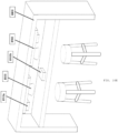
- FIGS. 16A-E illustrate an LED device 8050 useable as a light source in a nail lamp of embodiments of the present invention.
- the nail lamp includes an LED device 8050, a light source support 8900, and a controller 8910a, 8910b.
- the LED device 8050 is arranged within the light source support 8900, and the controller 8910a may be arranged on the light source support 8900 or the controller 8910b may be external to the light source support 8900, such as a wired or wireless controller.
- the light source support 8900 may be connectably mountable to the underside of a piece of furniture 8800, for example, a shelf on table, desk, and the like.
- the light source support 8900 may be connectably mountable through the use of an external mount, screws, clamps, adhesives, or any other connecting hardware or material.
- the light source support 8900 may be connected to a nail lamp base, such as the nail lamp embodiments described herein, particularly the lamps 6010 and 7010.
- the LED device 8050 is a multiple-wavelength LED device.
- the LED device 8050 includes a circuit board 8300 with a plurality of semiconductor chips 8310 coupled thereto. While four semiconductor chips 8310 are shown on the circuit board 8300 in FIGS. 16A and 16D , the LED device 8050 may have a different number of chips. In the embodiment shown in FIGS. 16A-D , four chips 8310 are coupled to the circuit board 8300. The four chips 8310 and the circuit board 8300 are at least partially covered by a protective encapsulant or lens 8320. For example, the lens 8320 covers at least the four semiconductor chips 8310.
- the lens 8320 may be made of a transparent material, such as plastic, glass, and the like, in order to protect the chips 8310.
- the lens 8320 may be hemispherically shaped with a large light disbursement or beam angle (e.g., a 135° disbursement angle), or may alternatively be a cylindrically shaped with a domed end, which has a lower light disbursement or beam angle (e.g., a 65° disbursement angle).
- a large light disbursement or beam angle e.g., a 135° disbursement angle
- a domed end which has a lower light disbursement or beam angle (e.g., a 65° disbursement angle).
- At least one of the chips 8310 has a peak electromagnetic emission intensity at a wavelength of approximately 380-390 nm, and at least one of the chips 8310 has a peak electromagnetic emission intensity at a wavelength of approximately 395-415 nm.
- the lower wavelength chip(s) 8310 i.e., the 380-390 nm chip(s)
- the higher wavelength chip(s) 8310 i.e., the 395-415 nm chip(s)
- the four chips 8310 may include a combination of one 380-390 nm chip and three 395-415 nm chips, two 380-390 nm chips and two 395-415 nm chips, or three 380-390 nm chips and one 395-415 nm chip.
- the LED device 8050 may have chips emitting at other wavelengths suitable for curing light-curable nail products of different types.
- the LED device 8050 may include two, three, four, five, etc., chips.
- the LED device 8050 may include eight chips, with the chips emitting at some combination of 365 nm, 375 nm, 385 nm, 395 nm, 405 nm, 415 nm, 425 nm, etc., wavelengths.
- the LED devices 8050 just described may be, for example, those available from SemiLEDs Corp. (Taiwan) as model number N5050U-UNL2-A1G41H (hemispherical) or model N5050U-UNF2-A1G41H (cylindrical with dome-shaped end).
- the LED devices 8050 may include chips all having the same peak intensity wavelength, or may include semiconductor chips having different peak intensity wavelengths.
- the LED device 8050 is connected to and controlled by an electronic controller (not shown).
- a controller interface is included on the nail lamp (e.g., 6010, 7010, 8010) to enable an operator to input instructions to the controller.
- the controller interface may include any combination of control buttons, a control dial, a digital input pad, and the like, located on the base or another location of the nail lamp.
- the controller may be a CPU programmed to alter the emission intensities of the LED device(s) 8050 by controlling current to the LED device(s) 8050.
- the controller may be used to set the LED device(s) 8050 to a 100% intensity, an intermediate intensity (e.g., 40%, 50%, 60%, 75%, 90%), or no intensity at all (e.g., an "off' state).
- the controller may control the LED device(s) 8050 as a whole (i.e., all four chips 8310 simultaneously), or the controller may control each chip 8310 individually, or the controller may control a combination of chips 8310 together.
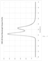
- FIG. 17 depicts the relative peak intensity wavelength profile of a multiple-wavelength LED device. As shown, a first peak intensity at a wavelength of approximately 385 nm is relatively higher than a second peak intensity at a wavelength of approximately 405 nm.
- the aforementioned light sources may be pulsable in accordance with a pulsing sequence. Pulsing is used with a multiple-wavelength LED device.
- the LED device(s) may all be pulsed simultaneously, or the LED devices may each be individually pulsed according to a different sequence.
- the light sources are pulsable between a first intensity and a second intensity.
- the first intensity may be a peak intensity (100%), or an intensity lower than a peak intensity
- the second intensity may be no intensity, or something higher than no intensity but lower than the first intensity.
- the first intensity may be 90-100% of a maximum intensity.
- the first intensity may be 90-100% of a maximum intensity and the second intensity may be 40-60%. of a maximum intensity.
- the LED devices useable in the embodiments described herein typically have an intensity range between 0 microwatts/cm 2 and 600 microwatts/cm 2 .
- the light sources may be pulsable between 600 microwatts/cm 2 and 0 microwatts/cm 2 , pulsable between 500 microwatts/cm 2 and 200 microwatts/cm 2 , or pulsable between any other intensities (e.g., 600 microwatts/cm 2 and 500 microwatts/cm 2 , 400 microwatts/cm 2 and 200 microwatts/cm 2 , 300 microwatts/cm 2 and 0 microwatts/cm 2 , etc..
- the light sources is pulsable between the first intensity and the second intensity according to a predetermined sequence.
- the controller may is used to adjust the intensities from the first intensity, after a predetermined amount of time, to the second intensity, and then stay at the second intensity for a predetermined amount of time.
- the controller may be used to have the light sources emit at a peak intensity for a period of time between 0.01 and 5.0 seconds, and have the light sources emit at zero intensity (i.e., turn the light sources off) for a period of time between 0.01 and 10.0 seconds.
- the period of time for the first intensity and the second intensity may be of the same duration or of different durations.
- the light sources may be pulsed for a single sequence (i.e., between a first and second intensity for the predetermined amount of time), or may be repeatedly pulsed according to the sequence for a predetermined amount of time or number of cycles.
- the controller may be used to have the light sources emit at an intensity of 600 microwatts/cm 2 for 5.0 seconds (i.e., time period from 0.0 to 5.0 seconds), turn the light sources off for 10.0 seconds (i.e., time period 5.0-15.0 seconds), and repeat this cycle for a time period of 60.0 seconds.
- the time durations mentioned above are 5.0 seconds and 10.0 seconds, respectively, these time durations are merely examples. Other duration values may be used.
- the light source is pulsable according to the following pulsing sequence: the light source is first operated at a first intensity that is 40-60% of a maximum intensity for a first duration of 0.01 to 5.0 seconds, and is then operated at a second intensity of 0% ("zero intensity") for a second duration of 0.01 to 10.0 seconds. This pulsing sequence is repeated for a duration of 60.0 seconds.
- the light source is pulsable according to the following pulsing sequence: the light source is first operated at a first intensity that is 40-60% of a maximum intensity for a first duration of 0.5 to 2.0 seconds, and is then operated at a second intensity of 0% ("zero intensity") for a second duration of 0.5 to 5.0 seconds. This pulsing sequence is repeated for a duration of approximately 4.0 to 20.0 seconds.
- the light source is pulsable according to the following pulsing sequence: the light source is first operated at a first intensity that is 40-60% of a maximum intensity for a first duration of 0.01 to 5.0 seconds, and is then operated at a second intensity that is 90-100%. of the maximum intensity for a second duration of 0.01 to 10.0 seconds. This pulsing sequence is repeated for a duration of 60.0 seconds.
- the light source is pulsable according to the following pulsing sequence: the light source is first operated at a first intensity that is 40-60% of a maximum intensity for a first duration of 0.5 to 2.0 seconds, and is then operated at a second intensity that is 90-100% of the maximum intensity for a second duration of 0.5 to 5.0 seconds. This pulsing sequence is repeated for a duration of approximately 4.0 to 20.0 seconds.
- the light source is pulsable according to the following pulsing sequence: the light source is first operated at a first intensity that is 90-100% of a maximum intensity for a first duration of 0.01 to 5.0 seconds, and is then operated at a second intensity of 0% ("zero intensity") for a second duration of 0.01 to 10.0 seconds. This pulsing sequence is repeated for a duration of 60.0 seconds.
- the light source is pulsable according to the following pulsing sequence: the light source is first operated at a first intensity that is 90-100% of a maximum intensity for a first duration of 0.5 to 2.0 seconds, and is then operated at a second intensity of 0% ("zero intensity") for a second duration of 0.5 to 5.0 seconds. This pulsing sequence is repeated for a duration of approximately 4.0 to 20.0 seconds.
- the light source is pulsable according to the following pulsing sequence: the light source is first operated at a first intensity that is 90-100% of a maximum intensity for a first duration of 0.01 to 5.0 seconds, and is then operated at a second intensity of 40-60% of the maximum intensity for a second duration of 0.01 to 10.0 seconds. This pulsing sequence is repeated for a duration of 60.0 seconds.
- the light source is pulsable according to the following pulsing sequence: the light source is first operated at a first intensity that is 90-100% of a maximum intensity for a first duration of 0.5 to 2.0 seconds, and is then operated at a second intensity of 40-60% of the maximum intensity for a second duration of 0.5 to 5.0 seconds. This pulsing sequence is repeated for a duration of approximately 4.0 to 20.0 seconds.
- the light sources may be emitted at an intensity of 600 microwatts/cm 2 for 5.0 seconds, emitted at an intensity of 0 microwatts/cm2 for 10.0 seconds, emitted at an intensity of 400 microwatts/cm 2 for 3.0 seconds, etc.
- the light source is pulsable according to the following pulsing sequence: the light source is first operated at a first intensity that is 40-60% of a maximum intensity for a first duration of approximately 1.0 second, is then operated at a second intensity of 0% ("zero intensity") for a second duration of approximately 1.0 second, and then operated at a third intensity that is 90-100% of a maximum intensity for a third duration of approximately 50.0 seconds.
- This pulsing sequence is repeated for a duration of approximately 60 seconds.
- the light source may be controlled to operate continuously at one of the first, second, or third intensities for a predetermined amount of time.
- the light sources may remain at a certain intensity after the sequence until the controller turns off the light sources.
- the duration of the first intensity is from 0.5 seconds to 2.0 seconds
- the duration of the second intensity is from 0.5 to 5.0 seconds
- the length of time of the sequence is from 4.0-20.0 seconds.
- the light sources emit continuously for a total time period, including the pulsing sequence, of 60.0 seconds.
- the controller above may be coupled to a plurality of control buttons, control dials, digital input pads, and the like, located on the base or other location of the nail lamp. These control buttons, dials, etc., may be used to alter the intensities at which the light sources emit, as well as to control the pulsing sequences just described.
- the table below depicts examples of values for the control buttons used to adjust the intensity emissions of the lights sources as well as the pulsing sequences.
- Current Setting Relative Intensity (%) Button 1 Button 2 Button 3 Button 4 0.25A 48 10 second pulsing (1 sec. on, 1 sec. off) 10 second pulsing (1 sec. on, 1 sec. off); 50 seconds continuous 10 second pulsing (1 sec. on, 1 sec. off) 0.50A 96 60 seconds continuous 0.52A 100 50 seconds continuous
- Button 1 is used for a lower than peak intensity and for a 10 second pulsing sequence with no continuous lighting after the pulsing sequence.
- the light sources will emit at 48% of peak intensity for 1.0 second, emit at 0 intensity for 1.0 second (i.e., the light sources are turned off), and repeat for a total duration of 10.0 seconds (i.e., 5 cycles).
- this particular Button 1 shows a 10 second pulsing sequence with equal first intensity (48%) and second intensity (0%) time durations (i.e., 1 second on and 1 second off), it should be understood that Button 1 may alternatively have different durations for each of the intensities.
- Button 1 may be any duration pulsing sequence, and is not limited to a 10 second pulsing sequence.
- Button 1 may be a 20 second pulsing sequence with the light sources emitting at 48% of peak intensity for 2.0 seconds, emitting at 0 intensity for 1.0 second, and repeating this sequence.
- Button 1 may alternatively be pulsed between two intensities ( e.g. , 48% and 100%).
- Button 2 is used for a lower than peak intensity for a 10 second pulsing sequence followed by a duration of continuous lighting at the same intensity.
- Button 3 is used for a lower than peak intensity for a continuous amount of time with no pulsing.
- Button 4 pulses the light sources for a 10.0 second sequence at a first intensity, and then turns the light sources on at a peak intensity for a continuous amount of time.
- the values in the above table are exemplary only and should not be so limited.
- Buttons 1-4 it should be understood that any number of buttons may be used and each combination of pulsing sequences and emission intensities may correspond to an individual button.
- control dials, input pads, etc. may be used instead of the control buttons just described
- the controller may be used to alter the intensity at which one of the chips within the light source emits without altering the other chips. For example, the controller may reduce the reduce the current to the first chip to cause it to emit at an intensity less than peak intensity (i.e., less than 100%) while providing full current to the remaining chip(s) to cause them to emit at peak intensity (i.e., 100%).
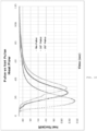
- FIGS. 18-19 show heat flow vs. time and accumulated exotherm vs. time, respectively, for light sources having no pulsing sequence, a 10 second pulsing sequence (pulsing 10 second on and 10 second off for 10.0 seconds), and a 20 second pulsing sequence (pulsing 1.0 second on and 1.0 second off for 20.0 seconds). All three samples have 60 seconds of continuous lighting after the pulse durations.
- a no pulse sequence has a relatively high heat flow compared to the 10 second pulsing sequence and the 20 second pulse sequence. Additionally, this relatively high heat flow occurs at a time period before the peak heat flows of both the 10 second pulsing sequence and the 20 second pulsing sequence.
- FIG. 19 shows the no pulse sequence resulting in a relatively high accumulated exothern1 at earlier times, while the 10 second pulsing sequence and 20 second pulsing sequence result in a significantly lower accumulated exotherm at initial stages of the curing process.
- the three sequences have approximate accumulated exotherm values, and by 420 seconds, the accumulated exotherm is almost identical for all three sequences.
- FIGS. 18-19 show that, overall, pulse sequences delay the peak time at which peak heat flow occurs, reduce the peak value of heat flow, reduce the accumulated exotherm during the periods of lighting, and result in the same total exotherm as the no pulse sequence.
- This pulsing sequence may be designed to efficiently cure nail product while avoiding heat-induced discomfort, or bums, to the user.
Landscapes
- Engineering & Computer Science (AREA)
- Mechanical Engineering (AREA)
- General Engineering & Computer Science (AREA)
- Life Sciences & Earth Sciences (AREA)
- Microbiology (AREA)
- Non-Portable Lighting Devices Or Systems Thereof (AREA)
- Radiation-Therapy Devices (AREA)
- Arrangement Of Elements, Cooling, Sealing, Or The Like Of Lighting Devices (AREA)
Applications Claiming Priority (3)
| Application Number | Priority Date | Filing Date | Title |
|---|---|---|---|
| US201462058865P | 2014-10-02 | 2014-10-02 | |
| US201462059585P | 2014-10-03 | 2014-10-03 | |
| PCT/US2015/053449 WO2016054346A1 (en) | 2014-10-02 | 2015-10-01 | Nail lamp |
Publications (3)
| Publication Number | Publication Date |
|---|---|
| EP3201929A1 EP3201929A1 (en) | 2017-08-09 |
| EP3201929A4 EP3201929A4 (en) | 2018-07-25 |
| EP3201929B1 true EP3201929B1 (en) | 2024-03-06 |
Family
ID=55631497
Family Applications (1)
| Application Number | Title | Priority Date | Filing Date |
|---|---|---|---|
| EP15846788.6A Active EP3201929B1 (en) | 2014-10-02 | 2015-10-01 | Nail lamp |
Country Status (13)
Families Citing this family (20)
| Publication number | Priority date | Publication date | Assignee | Title |
|---|---|---|---|---|
| US9841233B2 (en) | 2012-03-30 | 2017-12-12 | Creative Nail Design Inc. | Nail lamp |
| CN107210080B (zh) * | 2014-10-02 | 2020-08-28 | 露华浓消费品公司 | 指甲灯 |
| EP3216368A1 (en) * | 2016-03-09 | 2017-09-13 | Koninklijke Philips N.V. | Hair styling |
| JP6454019B2 (ja) * | 2016-05-06 | 2019-01-16 | 株式会社カネカ | 光照射システム及び擬似自然光照射部材 |
| USD864485S1 (en) * | 2016-12-20 | 2019-10-22 | Shenzhen Uvled Optical Technology Co., Ltd. | Fingernail dryer |
| US10946413B2 (en) * | 2017-04-14 | 2021-03-16 | Cosmex Co. Ltd. | Slow-start photocuring device and switch control module thereof |
| KR101941378B1 (ko) * | 2017-11-23 | 2019-01-22 | 안미정 | 네일 젤 경화장치 |
| EP3801120B1 (en) | 2018-06-11 | 2023-05-03 | Revlon Consumer Products Corporation | Nail lamp |
| US20210386179A1 (en) * | 2018-10-31 | 2021-12-16 | Seyhan YILMAZ | Nail polish machine that can be applied and dried on 5 fingers simultaneously |
| US11134813B2 (en) * | 2019-03-22 | 2021-10-05 | Applied Lacquer Industries Inc. | 2-in-1 nail lamp station |
| US10506861B1 (en) * | 2019-03-22 | 2019-12-17 | Carol MA | 2-in-1 nail lamp station |
| US11484107B2 (en) | 2019-05-28 | 2022-11-01 | Kupa, Inc. | Electronic nail file with digital control and display and system of operation |
| USD914982S1 (en) * | 2019-07-25 | 2021-03-30 | Kupa, Inc. | Gel curing lamp |
| US11969068B2 (en) * | 2019-07-25 | 2024-04-30 | Kupa, Inc. | Cordless nail gel curing lamp with interchangeable surface features |
| CN113306315B (zh) * | 2020-02-26 | 2024-03-08 | 凤凰电机公司 | 干燥装置 |
| US11330886B2 (en) * | 2020-06-30 | 2022-05-17 | Hung Ly | Gel polish curing assembly |
| US20230024415A1 (en) * | 2021-07-23 | 2023-01-26 | Nail Alliance, Llc | Uv led curing apparatus |
| US12452979B2 (en) | 2023-03-29 | 2025-10-21 | Kupa, Inc. | Multiple lighting mode LED lamp |
| USD1041762S1 (en) * | 2024-01-19 | 2024-09-10 | Shenzhen Haige Cross Border Technology Co., Ltd. | Nail treatment device |
| CN119629809B (zh) * | 2024-12-06 | 2025-06-24 | 东莞市爱比丽电器有限公司 | 一种美甲灯自动功率调节方法、美甲灯及系统 |
Citations (5)
| Publication number | Priority date | Publication date | Assignee | Title |
|---|---|---|---|---|
| US20020181947A1 (en) * | 1999-09-24 | 2002-12-05 | Densen Cao | Method for curing composite materials |
| WO2005068509A1 (en) * | 2004-01-07 | 2005-07-28 | Con-Trol-Cure, Inc. | Uv curing method and apparatus |
| US20130109001A1 (en) * | 2011-11-02 | 2013-05-02 | Helio Optoelectronics Corporation | High-luminance uv led nail lamp structure and led light source module thereof |
| US20140194955A1 (en) * | 2011-07-03 | 2014-07-10 | Gadi Presburger | Device and Method of Treating Fungal Nail Infections |
| US20140231848A1 (en) * | 2013-02-19 | 2014-08-21 | Michael A. Tischler | Engineered-phosphor led packages and related methods |
Family Cites Families (64)
| Publication number | Priority date | Publication date | Assignee | Title |
|---|---|---|---|---|
| US489489A (en) | 1893-01-10 | Folding bed | ||
| US431682A (en) | 1890-07-08 | Device for supplying superheated steam to furnaces | ||
| US300960A (en) | 1884-06-24 | Machine for coiling wire | ||
| US492447A (en) | 1893-02-28 | Curtain-fixture | ||
| US1491106A (en) | 1921-09-29 | 1924-04-22 | Mauro D Angelo | Vehicle signal |
| US2262774A (en) | 1937-07-07 | 1941-11-18 | American Mach & Foundry | Packaging cigarettes and the like |
| US2262274A (en) | 1939-07-08 | 1941-11-11 | Fingerlin Eugene | Fingernail drying device |
| US2218296A (en) | 1940-03-02 | 1940-10-15 | Amanda Vaughan | Manicure shield |
| US3179795A (en) * | 1962-09-20 | 1965-04-20 | Paula A Angle | Nail light bracelet |
| FR2193049B1 (cg-RX-API-DMAC7.html) | 1972-07-20 | 1974-12-27 | Rhone Poulenc Sa | |
| US3864847A (en) | 1974-06-20 | 1975-02-11 | Fred Friedman | Nail polish dryer |
| US4193209A (en) | 1978-09-28 | 1980-03-18 | Lovison Paula J | Fingernail dryer |
| US4754769A (en) | 1985-03-12 | 1988-07-05 | Salon Pro, Inc. | Nail dryer |
| USD300960S (en) | 1986-03-17 | 1989-05-02 | Billings Calvert W | Dryer for polished toenails |
| DE3727916A1 (de) | 1987-08-21 | 1989-03-02 | Kulzer & Co Gmbh | Fingernagel-bestrahlungsgeraet |
| US4967775A (en) | 1988-05-12 | 1990-11-06 | Kaiser Carol M | Transparent safety guard for manicurist use |
| US5249367A (en) * | 1988-08-23 | 1993-10-05 | Ultraset Limited Partnership | Nail drying apparatus and method therefor |
| FR2665343B1 (fr) * | 1990-07-31 | 1992-12-04 | Briee Serge | Seche ongles. |
| US5103845A (en) | 1990-10-31 | 1992-04-14 | Matthews Lynn M | Manicure shield |
| US5336128A (en) | 1993-08-12 | 1994-08-09 | Esau Birdsong | Nail technician's ventilator |
| US5515621A (en) * | 1994-06-23 | 1996-05-14 | Asr Affiliates, Inc. | Nail drying system |
| DE19901589C1 (de) | 1999-01-16 | 2001-02-08 | Professional Products M Nauman | Bestrahlungsvorrichtung, insbesondere UV-Tischlampe, zur Verfestigung von lichtaushärtendem Gel im Zuge einer Fingernagelbehandlung |
| USD431682S (en) | 1999-09-02 | 2000-10-03 | G-Intek Co., Ltd. | Nail polish dryer |
| US6618683B1 (en) | 2000-12-12 | 2003-09-09 | International Business Machines Corporation | Method and apparatus for calibrating an accelerometer-based navigation system |
| CA2340209C (en) * | 2001-03-09 | 2005-08-09 | Paul Meinschenk | Nail jackets |
| USD453858S1 (en) | 2001-03-30 | 2002-02-19 | Chieh-Chen Tsai | Nail dryer |
| US20020183810A1 (en) | 2001-06-04 | 2002-12-05 | Vlahos George J. | Light therapy equipment |
| USD487489S1 (en) | 2002-07-09 | 2004-03-09 | Bae Hyo-Man | Simulated eye for toys |
| USD489489S1 (en) | 2002-10-09 | 2004-05-04 | Ben M. Khalaj | Nail dryer |
| USD492447S1 (en) | 2003-04-30 | 2004-06-29 | The Dezac Group Limited | Nail treatment device |
| US7162811B2 (en) * | 2003-06-16 | 2007-01-16 | Delaney Diane E | Method for drying nails |
| US20060260628A1 (en) | 2003-09-01 | 2006-11-23 | Dickson Industrial Co. Ltd | Nail care apparatus |
| DE202004008982U1 (de) | 2004-06-05 | 2004-08-19 | Costrade Beauty Consulting Gmbh | Bestrahlungsgerät für Finger- oder Fußnägel |
| DE202006005790U1 (de) | 2006-04-08 | 2006-06-22 | Naumann, Stefan | Vorrichtung zum Aushärten von Fingernageladhäsivmitteln |
| US7712473B1 (en) | 2007-04-16 | 2010-05-11 | Robinson Stanwick C | Fingernail gel curation apparatus |
| US20090143842A1 (en) | 2007-11-02 | 2009-06-04 | Cumbie William E | Phototherapy Treatment and Device for Infections, Diseases, and Disorders |
| CN201227850Y (zh) | 2008-05-06 | 2009-04-29 | 乙泰企业有限公司 | 仿指甲用胶的固化装置 |
| US20100293805A1 (en) * | 2009-05-20 | 2010-11-25 | Pao-Min Chang | Nail gel solidification apparatus |
| RU90301U1 (ru) | 2009-09-21 | 2010-01-10 | Владимир Витальевич Ищенко | Светодиодный полимеризатор ногтевых гелей |
| JP2011098073A (ja) * | 2009-11-06 | 2011-05-19 | Kazuyoshi Azuma | 爪コート用ジェル乾燥機 |
| TW201119605A (en) | 2009-12-11 | 2011-06-16 | Genesis Photonics Inc | Nail care device. |
| JP5596173B2 (ja) | 2009-12-23 | 2014-09-24 | テレフオンアクチーボラゲット エル エム エリクソン(パブル) | 作成コスト削減のためのサービス選択 |
| US8312641B2 (en) * | 2010-04-16 | 2012-11-20 | Cosmex Co., Ltd. | UV LED curing appartus with improved illumination and timer control |
| US8993983B2 (en) * | 2010-05-13 | 2015-03-31 | Nail Alliance Llc | UV LED curing apparatus with improved housing and switch controller |
| JP5356321B2 (ja) * | 2010-06-28 | 2013-12-04 | 光▲いぇ▼科技股▲ふん▼有限公司 | 爪上に塗布したアクリルゲルを固化するuvled固化装置 |
| US9149106B2 (en) | 2010-11-02 | 2015-10-06 | Fa Young Park | Method and apparatus for enhancing UV gel nail application |
| US8835886B2 (en) * | 2011-01-24 | 2014-09-16 | Revlon Consumer Products Corporation | UV nail lamp |
| DE102011085291B4 (de) | 2011-07-08 | 2021-02-25 | Zumtobel Lighting Gmbh | Lichtbeeinflussungselement zur Beeinflussung der Lichtabgabe von im Wesentlichen punktförmigen Lichtquellen |
| USD661429S1 (en) | 2011-07-20 | 2012-06-05 | Benchmark Brands, Inc. | Toe straightener |
| US8242475B1 (en) | 2011-08-16 | 2012-08-14 | Cosmex Co., Ltd. | UV liquid gel solidifying device for nail art |
| USD661021S1 (en) | 2011-08-30 | 2012-05-29 | Ycc Products Inc. | UV LED curing machine for fingernail gels |
| US20130161531A1 (en) | 2011-12-22 | 2013-06-27 | Danny Lee Haile | Devices and methods for curing nail gels |
| US9841233B2 (en) * | 2012-03-30 | 2017-12-12 | Creative Nail Design Inc. | Nail lamp |
| JP5423831B2 (ja) * | 2012-04-04 | 2014-02-19 | パナソニック株式会社 | 樹脂硬化装置 |
| CN102935422A (zh) * | 2012-07-09 | 2013-02-20 | 南昌绿扬光电科技有限公司 | 一种紫外光led装置 |
| JP5435092B1 (ja) * | 2012-08-24 | 2014-03-05 | パナソニック株式会社 | 樹脂硬化装置及び光硬化樹脂を硬化する方法 |
| CN202778914U (zh) * | 2012-09-05 | 2013-03-13 | 光晔科技股份有限公司 | 光固装置的支撑结构 |
| US8450705B1 (en) | 2012-09-14 | 2013-05-28 | Power Digital Delight Co., Ltd. | Lighting apparatus for nail beauty |
| WO2014074608A1 (en) | 2012-11-06 | 2014-05-15 | Coty Inc. | Uv led lightbar setting uv-curable nail formulation |
| CN203801932U (zh) * | 2013-11-26 | 2014-09-03 | 光明半导体(天津)有限公司 | 指甲固化装置 |
| US9713371B1 (en) * | 2014-05-23 | 2017-07-25 | LeChat | Rechargeable LED nail lamp with light diffuser |
| CN107210080B (zh) * | 2014-10-02 | 2020-08-28 | 露华浓消费品公司 | 指甲灯 |
| US10517371B2 (en) * | 2016-06-14 | 2019-12-31 | L'oreal | Curing applicator |
| US10506861B1 (en) * | 2019-03-22 | 2019-12-17 | Carol MA | 2-in-1 nail lamp station |
-
2015
- 2015-10-01 CN CN201580065817.XA patent/CN107210080B/zh active Active
- 2015-10-01 SG SG11201702687SA patent/SG11201702687SA/en unknown
- 2015-10-01 AU AU2015324955A patent/AU2015324955A1/en not_active Abandoned
- 2015-10-01 RU RU2017114513A patent/RU2017114513A/ru not_active Application Discontinuation
- 2015-10-01 CA CA2967858A patent/CA2967858A1/en not_active Abandoned
- 2015-10-01 US US15/109,503 patent/US10247475B2/en active Active
- 2015-10-01 KR KR1020177011832A patent/KR20170071522A/ko not_active Withdrawn
- 2015-10-01 WO PCT/US2015/053449 patent/WO2016054346A1/en not_active Ceased
- 2015-10-01 MX MX2017004353A patent/MX2017004353A/es unknown
- 2015-10-01 EP EP15846788.6A patent/EP3201929B1/en active Active
- 2015-10-01 JP JP2017517684A patent/JP2017533007A/ja active Pending
-
2017
- 2017-04-02 IL IL251495A patent/IL251495A0/en unknown
- 2017-04-03 PH PH12017500607A patent/PH12017500607A1/en unknown
-
2019
- 2019-02-28 US US16/288,840 patent/US10876791B2/en active Active
Patent Citations (5)
| Publication number | Priority date | Publication date | Assignee | Title |
|---|---|---|---|---|
| US20020181947A1 (en) * | 1999-09-24 | 2002-12-05 | Densen Cao | Method for curing composite materials |
| WO2005068509A1 (en) * | 2004-01-07 | 2005-07-28 | Con-Trol-Cure, Inc. | Uv curing method and apparatus |
| US20140194955A1 (en) * | 2011-07-03 | 2014-07-10 | Gadi Presburger | Device and Method of Treating Fungal Nail Infections |
| US20130109001A1 (en) * | 2011-11-02 | 2013-05-02 | Helio Optoelectronics Corporation | High-luminance uv led nail lamp structure and led light source module thereof |
| US20140231848A1 (en) * | 2013-02-19 | 2014-08-21 | Michael A. Tischler | Engineered-phosphor led packages and related methods |
Also Published As
| Publication number | Publication date |
|---|---|
| AU2015324955A1 (en) | 2017-05-11 |
| KR20170071522A (ko) | 2017-06-23 |
| WO2016054346A1 (en) | 2016-04-07 |
| PH12017500607A1 (en) | 2017-09-04 |
| EP3201929A4 (en) | 2018-07-25 |
| CN107210080A (zh) | 2017-09-26 |
| RU2017114513A (ru) | 2018-11-02 |
| US20160370113A1 (en) | 2016-12-22 |
| US10876791B2 (en) | 2020-12-29 |
| SG11201702687SA (en) | 2017-04-27 |
| RU2017114513A3 (cg-RX-API-DMAC7.html) | 2019-05-15 |
| CN107210080B (zh) | 2020-08-28 |
| JP2017533007A (ja) | 2017-11-09 |
| MX2017004353A (es) | 2017-10-27 |
| IL251495A0 (en) | 2017-05-29 |
| EP3201929A1 (en) | 2017-08-09 |
| US20190195558A1 (en) | 2019-06-27 |
| US10247475B2 (en) | 2019-04-02 |
| CA2967858A1 (en) | 2016-04-07 |
Similar Documents
| Publication | Publication Date | Title |
|---|---|---|
| EP3201929B1 (en) | Nail lamp | |
| US11280545B2 (en) | Nail lamp | |
| US9533170B2 (en) | Multicolor light emitting diode treatment system with uniform illumination | |
| US8835886B2 (en) | UV nail lamp | |
| US8450705B1 (en) | Lighting apparatus for nail beauty | |
| AU615092B2 (en) | Fingernail irradiation instrument | |
| CA2475675A1 (en) | Reflective lighting apparatus with adjustable focus | |
| KR20170141219A (ko) | 속눈썹 연장부의 적용 시간을 감소시키기 위한 화학적으로 최소화된 시스템 | |
| EP3801120A1 (en) | Nail lamp | |
| WO2014030291A1 (ja) | 樹脂硬化装置および光硬化樹脂の硬化方法 | |
| JP5356321B2 (ja) | 爪上に塗布したアクリルゲルを固化するuvled固化装置 | |
| KR101318799B1 (ko) | 네일용 자외선 경화기 | |
| US20170143461A1 (en) | A dental light irradiation device | |
| HK1238408A1 (en) | Nail lamp | |
| HK1238408B (zh) | 指甲灯 | |
| US20230232957A1 (en) | Nail UV/LED Products Curing Lamp | |
| CN211092289U (zh) | 一种美甲灯 | |
| US20250311831A1 (en) | Uv nail lamp with light guide | |
| JP2011238748A (ja) | 紫外光発光ダイオード固化装置 | |
| CN209825543U (zh) | 一种竖式美甲led灯 | |
| EP3603566A1 (en) | A dental light polymerization device | |
| TWM464051U (zh) | 具節能效果的光固化裝置 |
Legal Events
| Date | Code | Title | Description |
|---|---|---|---|
| STAA | Information on the status of an ep patent application or granted ep patent |
Free format text: STATUS: THE INTERNATIONAL PUBLICATION HAS BEEN MADE |
|
| PUAI | Public reference made under article 153(3) epc to a published international application that has entered the european phase |
Free format text: ORIGINAL CODE: 0009012 |
|
| STAA | Information on the status of an ep patent application or granted ep patent |
Free format text: STATUS: REQUEST FOR EXAMINATION WAS MADE |
|
| 17P | Request for examination filed |
Effective date: 20170426 |
|
| AK | Designated contracting states |
Kind code of ref document: A1 Designated state(s): AL AT BE BG CH CY CZ DE DK EE ES FI FR GB GR HR HU IE IS IT LI LT LU LV MC MK MT NL NO PL PT RO RS SE SI SK SM TR |
|
| AX | Request for extension of the european patent |
Extension state: BA ME |
|
| RIN1 | Information on inventor provided before grant (corrected) |
Inventor name: PANOS, SERGIO GARCIA Inventor name: MOORE, DANIEL Inventor name: VALIA, DAVID Inventor name: VU, THONG Inventor name: FERRER, JUAN LUIS HEREDIA |
|
| DAV | Request for validation of the european patent (deleted) | ||
| DAX | Request for extension of the european patent (deleted) | ||
| A4 | Supplementary search report drawn up and despatched |
Effective date: 20180622 |
|
| RIC1 | Information provided on ipc code assigned before grant |
Ipc: F26B 3/28 20060101ALI20180618BHEP Ipc: A45D 29/00 20060101ALI20180618BHEP Ipc: G21K 5/08 20060101AFI20180618BHEP |
|
| RIN1 | Information on inventor provided before grant (corrected) |
Inventor name: MOORE, DANIEL Inventor name: VU, THONG Inventor name: PANOS, SERGIO GARCIA Inventor name: LEE, YIN-JUNG Inventor name: FERRER, JUAN LUIS HEREDIA Inventor name: VALIA, DAVID |
|
| TPAC | Observations filed by third parties |
Free format text: ORIGINAL CODE: EPIDOSNTIPA |
|
| STAA | Information on the status of an ep patent application or granted ep patent |
Free format text: STATUS: EXAMINATION IS IN PROGRESS |
|
| 17Q | First examination report despatched |
Effective date: 20210506 |
|
| RAP3 | Party data changed (applicant data changed or rights of an application transferred) |
Owner name: REVLON CONSUMER PRODUCTS LLC |
|
| REG | Reference to a national code |
Ref country code: DE Ref legal event code: R079 Free format text: PREVIOUS MAIN CLASS: G21K0005080000 Ipc: F26B0009000000 Ref document number: 602015087836 Country of ref document: DE |
|
| RIC1 | Information provided on ipc code assigned before grant |
Ipc: F26B 3/28 20060101ALI20231011BHEP Ipc: A45D 29/00 20060101ALI20231011BHEP Ipc: G21K 5/08 20060101ALI20231011BHEP Ipc: F26B 9/00 20060101AFI20231011BHEP |
|
| GRAP | Despatch of communication of intention to grant a patent |
Free format text: ORIGINAL CODE: EPIDOSNIGR1 |
|
| STAA | Information on the status of an ep patent application or granted ep patent |
Free format text: STATUS: GRANT OF PATENT IS INTENDED |
|
| INTG | Intention to grant announced |
Effective date: 20231122 |
|
| GRAS | Grant fee paid |
Free format text: ORIGINAL CODE: EPIDOSNIGR3 |
|
| GRAA | (expected) grant |
Free format text: ORIGINAL CODE: 0009210 |
|
| STAA | Information on the status of an ep patent application or granted ep patent |
Free format text: STATUS: THE PATENT HAS BEEN GRANTED |
|
| AK | Designated contracting states |
Kind code of ref document: B1 Designated state(s): AL AT BE BG CH CY CZ DE DK EE ES FI FR GB GR HR HU IE IS IT LI LT LU LV MC MK MT NL NO PL PT RO RS SE SI SK SM TR |
|
| REG | Reference to a national code |
Ref country code: GB Ref legal event code: FG4D |
|
| REG | Reference to a national code |
Ref country code: CH Ref legal event code: EP |
|
| REG | Reference to a national code |
Ref country code: IE Ref legal event code: FG4D |
|
| REG | Reference to a national code |
Ref country code: DE Ref legal event code: R096 Ref document number: 602015087836 Country of ref document: DE |
|
| P01 | Opt-out of the competence of the unified patent court (upc) registered |
Effective date: 20240313 |
|
| REG | Reference to a national code |
Ref country code: LT Ref legal event code: MG9D |
|
| PG25 | Lapsed in a contracting state [announced via postgrant information from national office to epo] |
Ref country code: LT Free format text: LAPSE BECAUSE OF FAILURE TO SUBMIT A TRANSLATION OF THE DESCRIPTION OR TO PAY THE FEE WITHIN THE PRESCRIBED TIME-LIMIT Effective date: 20240306 |
|
| REG | Reference to a national code |
Ref country code: NL Ref legal event code: MP Effective date: 20240306 |
|
| PG25 | Lapsed in a contracting state [announced via postgrant information from national office to epo] |
Ref country code: HR Free format text: LAPSE BECAUSE OF FAILURE TO SUBMIT A TRANSLATION OF THE DESCRIPTION OR TO PAY THE FEE WITHIN THE PRESCRIBED TIME-LIMIT Effective date: 20240306 Ref country code: RS Free format text: LAPSE BECAUSE OF FAILURE TO SUBMIT A TRANSLATION OF THE DESCRIPTION OR TO PAY THE FEE WITHIN THE PRESCRIBED TIME-LIMIT Effective date: 20240606 |
|
| PG25 | Lapsed in a contracting state [announced via postgrant information from national office to epo] |
Ref country code: ES Free format text: LAPSE BECAUSE OF FAILURE TO SUBMIT A TRANSLATION OF THE DESCRIPTION OR TO PAY THE FEE WITHIN THE PRESCRIBED TIME-LIMIT Effective date: 20240306 |
|
| PG25 | Lapsed in a contracting state [announced via postgrant information from national office to epo] |
Ref country code: RS Free format text: LAPSE BECAUSE OF FAILURE TO SUBMIT A TRANSLATION OF THE DESCRIPTION OR TO PAY THE FEE WITHIN THE PRESCRIBED TIME-LIMIT Effective date: 20240606 Ref country code: NO Free format text: LAPSE BECAUSE OF FAILURE TO SUBMIT A TRANSLATION OF THE DESCRIPTION OR TO PAY THE FEE WITHIN THE PRESCRIBED TIME-LIMIT Effective date: 20240606 Ref country code: LT Free format text: LAPSE BECAUSE OF FAILURE TO SUBMIT A TRANSLATION OF THE DESCRIPTION OR TO PAY THE FEE WITHIN THE PRESCRIBED TIME-LIMIT Effective date: 20240306 Ref country code: HR Free format text: LAPSE BECAUSE OF FAILURE TO SUBMIT A TRANSLATION OF THE DESCRIPTION OR TO PAY THE FEE WITHIN THE PRESCRIBED TIME-LIMIT Effective date: 20240306 Ref country code: FI Free format text: LAPSE BECAUSE OF FAILURE TO SUBMIT A TRANSLATION OF THE DESCRIPTION OR TO PAY THE FEE WITHIN THE PRESCRIBED TIME-LIMIT Effective date: 20240306 Ref country code: ES Free format text: LAPSE BECAUSE OF FAILURE TO SUBMIT A TRANSLATION OF THE DESCRIPTION OR TO PAY THE FEE WITHIN THE PRESCRIBED TIME-LIMIT Effective date: 20240306 Ref country code: BG Free format text: LAPSE BECAUSE OF FAILURE TO SUBMIT A TRANSLATION OF THE DESCRIPTION OR TO PAY THE FEE WITHIN THE PRESCRIBED TIME-LIMIT Effective date: 20240306 |
|
| REG | Reference to a national code |
Ref country code: AT Ref legal event code: MK05 Ref document number: 1663905 Country of ref document: AT Kind code of ref document: T Effective date: 20240306 |
|
| PG25 | Lapsed in a contracting state [announced via postgrant information from national office to epo] |
Ref country code: SE Free format text: LAPSE BECAUSE OF FAILURE TO SUBMIT A TRANSLATION OF THE DESCRIPTION OR TO PAY THE FEE WITHIN THE PRESCRIBED TIME-LIMIT Effective date: 20240306 Ref country code: LV Free format text: LAPSE BECAUSE OF FAILURE TO SUBMIT A TRANSLATION OF THE DESCRIPTION OR TO PAY THE FEE WITHIN THE PRESCRIBED TIME-LIMIT Effective date: 20240306 |
|
| PG25 | Lapsed in a contracting state [announced via postgrant information from national office to epo] |
Ref country code: NL Free format text: LAPSE BECAUSE OF FAILURE TO SUBMIT A TRANSLATION OF THE DESCRIPTION OR TO PAY THE FEE WITHIN THE PRESCRIBED TIME-LIMIT Effective date: 20240306 |
|
| PG25 | Lapsed in a contracting state [announced via postgrant information from national office to epo] |
Ref country code: NL Free format text: LAPSE BECAUSE OF FAILURE TO SUBMIT A TRANSLATION OF THE DESCRIPTION OR TO PAY THE FEE WITHIN THE PRESCRIBED TIME-LIMIT Effective date: 20240306 |
|
| PG25 | Lapsed in a contracting state [announced via postgrant information from national office to epo] |
Ref country code: IS Free format text: LAPSE BECAUSE OF FAILURE TO SUBMIT A TRANSLATION OF THE DESCRIPTION OR TO PAY THE FEE WITHIN THE PRESCRIBED TIME-LIMIT Effective date: 20240706 |
|
| PG25 | Lapsed in a contracting state [announced via postgrant information from national office to epo] |
Ref country code: PT Free format text: LAPSE BECAUSE OF FAILURE TO SUBMIT A TRANSLATION OF THE DESCRIPTION OR TO PAY THE FEE WITHIN THE PRESCRIBED TIME-LIMIT Effective date: 20240708 Ref country code: SM Free format text: LAPSE BECAUSE OF FAILURE TO SUBMIT A TRANSLATION OF THE DESCRIPTION OR TO PAY THE FEE WITHIN THE PRESCRIBED TIME-LIMIT Effective date: 20240306 |
|
| PG25 | Lapsed in a contracting state [announced via postgrant information from national office to epo] |
Ref country code: CZ Free format text: LAPSE BECAUSE OF FAILURE TO SUBMIT A TRANSLATION OF THE DESCRIPTION OR TO PAY THE FEE WITHIN THE PRESCRIBED TIME-LIMIT Effective date: 20240306 Ref country code: EE Free format text: LAPSE BECAUSE OF FAILURE TO SUBMIT A TRANSLATION OF THE DESCRIPTION OR TO PAY THE FEE WITHIN THE PRESCRIBED TIME-LIMIT Effective date: 20240306 |
|
| PG25 | Lapsed in a contracting state [announced via postgrant information from national office to epo] |
Ref country code: AT Free format text: LAPSE BECAUSE OF FAILURE TO SUBMIT A TRANSLATION OF THE DESCRIPTION OR TO PAY THE FEE WITHIN THE PRESCRIBED TIME-LIMIT Effective date: 20240306 |
|
| PG25 | Lapsed in a contracting state [announced via postgrant information from national office to epo] |
Ref country code: PL Free format text: LAPSE BECAUSE OF FAILURE TO SUBMIT A TRANSLATION OF THE DESCRIPTION OR TO PAY THE FEE WITHIN THE PRESCRIBED TIME-LIMIT Effective date: 20240306 |
|
| PG25 | Lapsed in a contracting state [announced via postgrant information from national office to epo] |
Ref country code: SK Free format text: LAPSE BECAUSE OF FAILURE TO SUBMIT A TRANSLATION OF THE DESCRIPTION OR TO PAY THE FEE WITHIN THE PRESCRIBED TIME-LIMIT Effective date: 20240306 |
|
| PG25 | Lapsed in a contracting state [announced via postgrant information from national office to epo] |
Ref country code: SM Free format text: LAPSE BECAUSE OF FAILURE TO SUBMIT A TRANSLATION OF THE DESCRIPTION OR TO PAY THE FEE WITHIN THE PRESCRIBED TIME-LIMIT Effective date: 20240306 Ref country code: SK Free format text: LAPSE BECAUSE OF FAILURE TO SUBMIT A TRANSLATION OF THE DESCRIPTION OR TO PAY THE FEE WITHIN THE PRESCRIBED TIME-LIMIT Effective date: 20240306 Ref country code: RO Free format text: LAPSE BECAUSE OF FAILURE TO SUBMIT A TRANSLATION OF THE DESCRIPTION OR TO PAY THE FEE WITHIN THE PRESCRIBED TIME-LIMIT Effective date: 20240306 Ref country code: PT Free format text: LAPSE BECAUSE OF FAILURE TO SUBMIT A TRANSLATION OF THE DESCRIPTION OR TO PAY THE FEE WITHIN THE PRESCRIBED TIME-LIMIT Effective date: 20240708 Ref country code: PL Free format text: LAPSE BECAUSE OF FAILURE TO SUBMIT A TRANSLATION OF THE DESCRIPTION OR TO PAY THE FEE WITHIN THE PRESCRIBED TIME-LIMIT Effective date: 20240306 Ref country code: IS Free format text: LAPSE BECAUSE OF FAILURE TO SUBMIT A TRANSLATION OF THE DESCRIPTION OR TO PAY THE FEE WITHIN THE PRESCRIBED TIME-LIMIT Effective date: 20240706 Ref country code: EE Free format text: LAPSE BECAUSE OF FAILURE TO SUBMIT A TRANSLATION OF THE DESCRIPTION OR TO PAY THE FEE WITHIN THE PRESCRIBED TIME-LIMIT Effective date: 20240306 Ref country code: CZ Free format text: LAPSE BECAUSE OF FAILURE TO SUBMIT A TRANSLATION OF THE DESCRIPTION OR TO PAY THE FEE WITHIN THE PRESCRIBED TIME-LIMIT Effective date: 20240306 Ref country code: AT Free format text: LAPSE BECAUSE OF FAILURE TO SUBMIT A TRANSLATION OF THE DESCRIPTION OR TO PAY THE FEE WITHIN THE PRESCRIBED TIME-LIMIT Effective date: 20240306 |
|
| PG25 | Lapsed in a contracting state [announced via postgrant information from national office to epo] |
Ref country code: IT Free format text: LAPSE BECAUSE OF FAILURE TO SUBMIT A TRANSLATION OF THE DESCRIPTION OR TO PAY THE FEE WITHIN THE PRESCRIBED TIME-LIMIT Effective date: 20240306 |
|
| REG | Reference to a national code |
Ref country code: DE Ref legal event code: R097 Ref document number: 602015087836 Country of ref document: DE |
|
| PG25 | Lapsed in a contracting state [announced via postgrant information from national office to epo] |
Ref country code: IT Free format text: LAPSE BECAUSE OF FAILURE TO SUBMIT A TRANSLATION OF THE DESCRIPTION OR TO PAY THE FEE WITHIN THE PRESCRIBED TIME-LIMIT Effective date: 20240306 |
|
| PLBE | No opposition filed within time limit |
Free format text: ORIGINAL CODE: 0009261 |
|
| STAA | Information on the status of an ep patent application or granted ep patent |
Free format text: STATUS: NO OPPOSITION FILED WITHIN TIME LIMIT |
|
| PG25 | Lapsed in a contracting state [announced via postgrant information from national office to epo] |
Ref country code: DK Free format text: LAPSE BECAUSE OF FAILURE TO SUBMIT A TRANSLATION OF THE DESCRIPTION OR TO PAY THE FEE WITHIN THE PRESCRIBED TIME-LIMIT Effective date: 20240306 |
|
| PG25 | Lapsed in a contracting state [announced via postgrant information from national office to epo] |
Ref country code: DK Free format text: LAPSE BECAUSE OF FAILURE TO SUBMIT A TRANSLATION OF THE DESCRIPTION OR TO PAY THE FEE WITHIN THE PRESCRIBED TIME-LIMIT Effective date: 20240306 |
|
| 26N | No opposition filed |
Effective date: 20241209 |
|
| PG25 | Lapsed in a contracting state [announced via postgrant information from national office to epo] |
Ref country code: SI Free format text: LAPSE BECAUSE OF FAILURE TO SUBMIT A TRANSLATION OF THE DESCRIPTION OR TO PAY THE FEE WITHIN THE PRESCRIBED TIME-LIMIT Effective date: 20240306 |
|
| REG | Reference to a national code |
Ref country code: DE Ref legal event code: R119 Ref document number: 602015087836 Country of ref document: DE |
|
| REG | Reference to a national code |
Ref country code: CH Ref legal event code: PL |
|
| PG25 | Lapsed in a contracting state [announced via postgrant information from national office to epo] |
Ref country code: MC Free format text: LAPSE BECAUSE OF FAILURE TO SUBMIT A TRANSLATION OF THE DESCRIPTION OR TO PAY THE FEE WITHIN THE PRESCRIBED TIME-LIMIT Effective date: 20240306 |
|
| PG25 | Lapsed in a contracting state [announced via postgrant information from national office to epo] |
Ref country code: DE Free format text: LAPSE BECAUSE OF NON-PAYMENT OF DUE FEES Effective date: 20250501 |
|
| PG25 | Lapsed in a contracting state [announced via postgrant information from national office to epo] |
Ref country code: BE Free format text: LAPSE BECAUSE OF NON-PAYMENT OF DUE FEES Effective date: 20241031 Ref country code: LU Free format text: LAPSE BECAUSE OF NON-PAYMENT OF DUE FEES Effective date: 20241001 |
|
| PG25 | Lapsed in a contracting state [announced via postgrant information from national office to epo] |
Ref country code: FR Free format text: LAPSE BECAUSE OF NON-PAYMENT OF DUE FEES Effective date: 20241031 |
|
| PG25 | Lapsed in a contracting state [announced via postgrant information from national office to epo] |
Ref country code: CH Free format text: LAPSE BECAUSE OF NON-PAYMENT OF DUE FEES Effective date: 20241031 |
|
| REG | Reference to a national code |
Ref country code: BE Ref legal event code: MM Effective date: 20241031 |
|
| PG25 | Lapsed in a contracting state [announced via postgrant information from national office to epo] |
Ref country code: IE Free format text: LAPSE BECAUSE OF NON-PAYMENT OF DUE FEES Effective date: 20241001 |
|
| PGFP | Annual fee paid to national office [announced via postgrant information from national office to epo] |
Ref country code: GB Payment date: 20251027 Year of fee payment: 11 |
|
| PG25 | Lapsed in a contracting state [announced via postgrant information from national office to epo] |
Ref country code: CY Free format text: LAPSE BECAUSE OF FAILURE TO SUBMIT A TRANSLATION OF THE DESCRIPTION OR TO PAY THE FEE WITHIN THE PRESCRIBED TIME-LIMIT; INVALID AB INITIO Effective date: 20151001 |
|
| PG25 | Lapsed in a contracting state [announced via postgrant information from national office to epo] |
Ref country code: HU Free format text: LAPSE BECAUSE OF FAILURE TO SUBMIT A TRANSLATION OF THE DESCRIPTION OR TO PAY THE FEE WITHIN THE PRESCRIBED TIME-LIMIT; INVALID AB INITIO Effective date: 20151001 |