EP3201663B1 - Optoelectronic component - Google Patents
Optoelectronic component Download PDFInfo
- Publication number
- EP3201663B1 EP3201663B1 EP15812943.7A EP15812943A EP3201663B1 EP 3201663 B1 EP3201663 B1 EP 3201663B1 EP 15812943 A EP15812943 A EP 15812943A EP 3201663 B1 EP3201663 B1 EP 3201663B1
- Authority
- EP
- European Patent Office
- Prior art keywords
- chip
- substrate
- waveguide
- optical
- component
- Prior art date
- Legal status (The legal status is an assumption and is not a legal conclusion. Google has not performed a legal analysis and makes no representation as to the accuracy of the status listed.)
- Active
Links
- 230000005693 optoelectronics Effects 0.000 title claims description 45
- 239000000758 substrate Substances 0.000 claims description 83
- 230000003287 optical effect Effects 0.000 claims description 38
- 239000004020 conductor Substances 0.000 claims description 24
- 230000005855 radiation Effects 0.000 claims description 20
- VYPSYNLAJGMNEJ-UHFFFAOYSA-N Silicium dioxide Chemical compound O=[Si]=O VYPSYNLAJGMNEJ-UHFFFAOYSA-N 0.000 claims description 16
- 229910052710 silicon Inorganic materials 0.000 claims description 15
- 239000010703 silicon Substances 0.000 claims description 15
- XUIMIQQOPSSXEZ-UHFFFAOYSA-N Silicon Chemical compound [Si] XUIMIQQOPSSXEZ-UHFFFAOYSA-N 0.000 claims description 14
- 239000013307 optical fiber Substances 0.000 claims description 14
- 235000012239 silicon dioxide Nutrition 0.000 claims description 8
- 239000000377 silicon dioxide Substances 0.000 claims description 8
- 239000004065 semiconductor Substances 0.000 claims description 6
- 230000008878 coupling Effects 0.000 claims description 4
- 238000010168 coupling process Methods 0.000 claims description 4
- 238000005859 coupling reaction Methods 0.000 claims description 4
- 239000000463 material Substances 0.000 description 9
- 239000000835 fiber Substances 0.000 description 6
- 241000219739 Lens Species 0.000 description 5
- 238000005516 engineering process Methods 0.000 description 4
- 230000005540 biological transmission Effects 0.000 description 3
- 238000004382 potting Methods 0.000 description 2
- 238000011084 recovery Methods 0.000 description 2
- 240000004322 Lens culinaris Species 0.000 description 1
- 230000002457 bidirectional effect Effects 0.000 description 1
- 239000000919 ceramic Substances 0.000 description 1
- 238000004891 communication Methods 0.000 description 1
- 238000010276 construction Methods 0.000 description 1
- 239000003365 glass fiber Substances 0.000 description 1
- 238000009434 installation Methods 0.000 description 1
- 239000012212 insulator Substances 0.000 description 1
- 230000010354 integration Effects 0.000 description 1
- 238000000034 method Methods 0.000 description 1
- 238000004377 microelectronic Methods 0.000 description 1
- 229920000642 polymer Polymers 0.000 description 1
- 238000007493 shaping process Methods 0.000 description 1
- 230000008054 signal transmission Effects 0.000 description 1
- 150000003376 silicon Chemical class 0.000 description 1
- 230000007704 transition Effects 0.000 description 1
Images


Classifications
-
- G—PHYSICS
- G02—OPTICS
- G02B—OPTICAL ELEMENTS, SYSTEMS OR APPARATUS
- G02B6/00—Light guides; Structural details of arrangements comprising light guides and other optical elements, e.g. couplings
- G02B6/10—Light guides; Structural details of arrangements comprising light guides and other optical elements, e.g. couplings of the optical waveguide type
- G02B6/12—Light guides; Structural details of arrangements comprising light guides and other optical elements, e.g. couplings of the optical waveguide type of the integrated circuit kind
- G02B6/12004—Combinations of two or more optical elements
-
- G—PHYSICS
- G02—OPTICS
- G02B—OPTICAL ELEMENTS, SYSTEMS OR APPARATUS
- G02B6/00—Light guides; Structural details of arrangements comprising light guides and other optical elements, e.g. couplings
- G02B6/24—Coupling light guides
- G02B6/26—Optical coupling means
- G02B6/30—Optical coupling means for use between fibre and thin-film device
-
- G—PHYSICS
- G02—OPTICS
- G02B—OPTICAL ELEMENTS, SYSTEMS OR APPARATUS
- G02B6/00—Light guides; Structural details of arrangements comprising light guides and other optical elements, e.g. couplings
- G02B6/24—Coupling light guides
- G02B6/42—Coupling light guides with opto-electronic elements
- G02B6/4201—Packages, e.g. shape, construction, internal or external details
- G02B6/4204—Packages, e.g. shape, construction, internal or external details the coupling comprising intermediate optical elements, e.g. lenses, holograms
- G02B6/4214—Packages, e.g. shape, construction, internal or external details the coupling comprising intermediate optical elements, e.g. lenses, holograms the intermediate optical element having redirecting reflective means, e.g. mirrors, prisms for deflecting the radiation from horizontal to down- or upward direction toward a device
-
- G—PHYSICS
- G02—OPTICS
- G02B—OPTICAL ELEMENTS, SYSTEMS OR APPARATUS
- G02B6/00—Light guides; Structural details of arrangements comprising light guides and other optical elements, e.g. couplings
- G02B6/24—Coupling light guides
- G02B6/42—Coupling light guides with opto-electronic elements
- G02B6/4201—Packages, e.g. shape, construction, internal or external details
- G02B6/4274—Electrical aspects
- G02B6/428—Electrical aspects containing printed circuit boards [PCB]
-
- G—PHYSICS
- G02—OPTICS
- G02B—OPTICAL ELEMENTS, SYSTEMS OR APPARATUS
- G02B6/00—Light guides; Structural details of arrangements comprising light guides and other optical elements, e.g. couplings
- G02B6/24—Coupling light guides
- G02B6/42—Coupling light guides with opto-electronic elements
- G02B6/43—Arrangements comprising a plurality of opto-electronic elements and associated optical interconnections
-
- G—PHYSICS
- G02—OPTICS
- G02B—OPTICAL ELEMENTS, SYSTEMS OR APPARATUS
- G02B6/00—Light guides; Structural details of arrangements comprising light guides and other optical elements, e.g. couplings
- G02B6/10—Light guides; Structural details of arrangements comprising light guides and other optical elements, e.g. couplings of the optical waveguide type
- G02B6/12—Light guides; Structural details of arrangements comprising light guides and other optical elements, e.g. couplings of the optical waveguide type of the integrated circuit kind
- G02B2006/12083—Constructional arrangements
- G02B2006/12107—Grating
Landscapes
- Physics & Mathematics (AREA)
- General Physics & Mathematics (AREA)
- Optics & Photonics (AREA)
- Engineering & Computer Science (AREA)
- Microelectronics & Electronic Packaging (AREA)
- Optical Integrated Circuits (AREA)
- Optical Couplings Of Light Guides (AREA)
Description
Die Erfindung bezieht sich auf ein optoelektronisches Bauelement mit den Merkmalen gemäß dem Oberbegriff des Patentanspruchs 1.The invention relates to an optoelectronic component having the features according to the preamble of claim 1.
Ein derartiges Bauelement ist in der Druckschrift "
Ein anderes Bauelement ist aus der US-Offenlegungsschrift
Die Druckschrift "
Heutzutage erhältliche optische Sende-Empfangs-Geräte, in Fachkreisen "Transceiver" genannt, dienen als Sender und Empfänger zur Umwandlung von elektrischen Datensignalen in elektrische Signale und umgekehrt. Die Hauptschwierigkeit besteht darin, dass eine integrierte Baugruppe, in Fachkreisen "Package" genannt, für ein optisches Sende-Empfangs-Gerät einerseits die photonisch integrierten Schaltkreise, bestehend aus Wellenleitern, optisch aktiven und optisch passiven Komponenten, wie Modulatoren, Photodioden, Teilern und Lichtkopplern bereitstellen muss. Andererseits sind elektronische Bauteile wie Modulatortreiber, Transimpedanzverstärker (TIA), Begrenzungsverstärker, in Fachkreisen "Limiting Amplifier" genannt (LA), Takt- und Datenrückgewinnung, in Fachkreisen "Clock and Data Recovery" genannt (CDR) und Entzerrer, in Fachkreisen "Equalizer" genannt, erforderlich, für die bereits hochentwickelte Verbindungstechniken aus der Mikroelektronik existieren. Diese Vielzahl an unterschiedlichen Komponenten soll möglichst kompakt und energiesparend in einem gemeinsamen Formfaktor untergebracht werden, bei geringen elektrischen und optischen Verlusten und unter Verwendung kostengünstiger Aufbautechnik. Gleichzeitig muss eine effiziente Skalierbarkeit hin zu höheren Übertragungsraten und Stückzahlen Teil des Gesamtkonzepts sein.Optical transceiver devices available nowadays, known in specialist circles as "transceivers", serve as transmitters and receivers for converting electrical data signals into electrical signals and vice versa. The main difficulty lies in the fact that an integrated assembly, known in specialist circles as a "package", consists of the photonic integrated circuits for an optical transceiver on the one hand of waveguides, optically active and optically passive components such as modulators, photodiodes, splitters and light couplers. On the other hand, electronic components such as modulator drivers, transimpedance amplifiers (TIA), limiting amplifiers, known in specialist circles as "Limiting Amplifiers" (LA), clock and data recovery, known in specialist circles as "Clock and Data Recovery" (CDR) and equalizers, and in specialist circles as "Equalizers" called, necessary, for which highly developed connection technologies from microelectronics already exist. This multitude of different Components should be accommodated as compactly and energy-efficiently as possible in a common form factor, with low electrical and optical losses and using inexpensive construction technology. At the same time, efficient scalability towards higher transmission rates and quantities must be part of the overall concept.
Die einzelnen Chips des Sende-Empfangs-Geräts können bekanntermaßen per Drahtbonden, in Fachkreisen "Wire-Bonding" genannt, oder Einbau über Kopf ohne Bonddrähte, in Fachkreisen "Flip Chip" genannt, auf ein Verdrahtungssubstrat, in Fachkreisen "Interposer" genannt, das z.B. aus Silizium, Keramik oder einem Polymer besteht, oder direkt auf ein Substrat, das zumeist aus einer PCB-Platine besteht, aufgebracht und elektrisch kontaktiert werden. Dabei existieren Varianten, bei denen die Glasfasern durch eine Öffnung im Verdrahtungssubstrat oder Substrat zum optischen Chip geführt werden [1, 2] oder von oben in einen Bereich, der frei von elektrischen Kontaktflächen ist. Ebenfalls entwickelt werden Lösungen, bei denen optische Signale in ein Verdrahtungssubstrat [3], oder bei manchen Konzepten in ein Substrat [1], eingekoppelt, dort geführt und von dort wieder ausgekoppelt werden. Der erhebliche Nachteil dabei liegt in den langen Signalwegen mit entsprechenden Dämpfungsverlusten und Koppelverlusten an jedem Übergang. Alleine diese zusätzlichen Verluste können dazu führen, dass das Ende-zu-Ende Leistungsbudget für die gesamte Übertragungsstrecke keine Reserve mehr lässt für die Verluste, die in dem eigentlichen Übertragungsmedium, in der Regel einer optischen Faser, auftreten können.As is known, the individual chips of the transceiver can be wired, known in specialist circles as "wire bonding", or overhead installation without bonding wires, known in specialist circles as "flip chip", onto a wiring substrate, known in specialist circles as "interposer" For example, made of silicon, ceramic or a polymer, or applied directly to a substrate, which mostly consists of a PCB, and electrically contacted. There are variants in which the glass fibers are guided through an opening in the wiring substrate or substrate to the optical chip [1, 2] or from above into an area that is free of electrical contact surfaces. Solutions are also being developed in which optical signals are coupled into a wiring substrate [3] or, in some concepts, into a substrate [1], guided there and then coupled out again. The significant disadvantage here is the long signal paths with corresponding attenuation losses and coupling losses at each transition. These additional losses alone can mean that the end-to-end power budget for the entire transmission path no longer leaves a reserve for the losses that can occur in the actual transmission medium, usually an optical fiber.
In aktuellen kommerziellen optischen Sende-Empfangs-Geräten, die zumeist auf der Signalübertragung in multimodalen Fasern basieren, befinden sich diverse diskrete optische Komponenten zur Strahlumlenkung und -formung, wie Mikrolinsen, Mikroprismen, Strahlteiler und Umlenkspiegel. Diese Bauteile müssen maschinell auf einem Träger platziert und befestigt werden, was einer einfachen Skalierbarkeit im Weg steht.In current commercial optical transceiver devices, which are mostly based on signal transmission in multimodal fibers, there are various discrete optical components for beam deflection and shaping, such as microlenses, microprisms, beam splitters and deflecting mirrors. These components have to be placed and fastened by machine on a carrier, which stands in the way of easy scalability.
Der Erfindung liegt ausgehend von dem beschriebenen Stand der Technik die Aufgabe zugrunde, ein optoelektronisches Bauelement anzugeben, das einen einfachen und kostengünstigen Gesamtaufbau aufweist.On the basis of the prior art described, the invention is based on the object of specifying an optoelectronic component which has a simple and inexpensive overall structure.
Diese Aufgabe wird erfindungsgemäß durch ein optoelektronisches Bauelement mit den Merkmalen gemäß Patentanspruch 1 gelöst. Vorteilhafte Ausgestaltungen des erfindungsgemäßen optoelektronischen Bauelements sind in Unteransprüchen angegeben.According to the invention, this object is achieved by an optoelectronic component having the features according to patent claim 1. Advantageous configurations of the optoelectronic component according to the invention are specified in the subclaims.
Erfindungsgemäß ist der Chip mit seiner Unterseite auf einer Leiterplatte aufgesetzt, die eine Verdrahtungsebene für die auf der Substratrückseite befindlichen elektrischen Leiterbahnanschlüsse bildet. Die Leiterplatte weist zumindest eine Verbindungsleitung auf, die den mit der elektrischen Komponente verbundenen Leiterbahnanschluss und den mit der elektrooptischen Komponente verbundenen Leiterbahnanschluss miteinander elektrisch verbindet.According to the invention, the underside of the chip is placed on a printed circuit board which forms a wiring plane for the electrical conductor track connections located on the back of the substrate. The circuit board has at least one connection line which electrically connects the conductor track connection connected to the electrical component and the conductor track connection connected to the electro-optical component to one another.
Besonders vorteilhaft ist es also, wenn zumindest einer der optischen Anschlüsse, vorzugsweise alle optischen Anschlüsse, auf der Chipoberseite des Chips angeordnet sind und zumindest einer der elektrischen Anschlüsse, vorzugsweise alle elektrischen Anschlüsse, auf der Chipunterseite des Chips angeordnet sind.It is therefore particularly advantageous if at least one of the optical connections, preferably all of the optical connections, are arranged on the top of the chip and at least one of the electrical connections, preferably all of the electrical connections, are arranged on the underside of the chip.
Die monolithisch integrierte elektrooptische Komponente ist bevorzugt ein Photodetektor oder ein Modulator.The monolithically integrated electro-optical component is preferably a photodetector or a modulator.
Vorzugsweise ist der integrierte Wellenleiter mit einer Umlenkeinrichtung ausgestattet oder steht mit einer solchen in Verbindung, die aus dem Wellenleiter auszukoppelnde optische Strahlung nahezu senkrecht in Richtung Chipoberseite umlenkt, oder Strahlung, die von der Chipoberseite nahezu senkrecht eintrifft, umlenkt und in den Wellenleiter einkoppelt.The integrated waveguide is preferably equipped with a deflection device or is connected to one that deflects optical radiation to be coupled out from the waveguide almost perpendicularly towards the top of the chip, or radiation that arrives from the top of the chip, deflects and couples it into the waveguide.
Die Umlenkeinrichtung ist bevorzugt durch einen in dem Wellenleiter ausgebildeten Gitterkoppler gebildet.The deflecting device is preferably formed by a grating coupler formed in the waveguide.
Als Chip-Basismaterial wird vorzugsweise SOI(Silicon-On-Insulator)-Material eingesetzt. Demgemäß wird es als vorteilhaft angesehen, wenn sich auf dem Substrat eine Siliziumdioxidschicht und darüber eine Siliziumdeckschicht befindet und der optische Wellenleiter und die elektrooptische Komponente in der Siliziumdeckschicht integriert sind.SOI (silicon-on-insulator) material is preferably used as the chip base material. Accordingly, it is considered advantageous if there is a silicon dioxide layer on the substrate and a silicon cover layer above it, and the optical waveguide and the electro-optical component are integrated in the silicon cover layer.
Die monolithisch integrierte elektrische Komponente ist bevorzugt ein Verstärker oder ein Treiber.The monolithically integrated electrical component is preferably an amplifier or a driver.
Bei einer besonders bevorzugten Ausgestaltung des optoelektronischen Bauelements ist vorgesehen, dass der mindestens eine integrierte Wellenleiter oder zumindest einer der integrierten Wellenleiter im Bereich eines seiner Wellenleiterenden mit einer Umlenkeinrichtung ausgestattet ist oder mit einer solchen in Verbindung steht, die von einer auf der Chipoberseite des Chips angeordneten Lichtquelle kommende und nahezu senkrecht zur Chipoberseite eintreffende optische Strahlung in den Wellenleiter einkoppelt, und im Bereich des anderen Wellenleiterendes mit einer Umlenkeinrichtung ausgestattet ist oder mit einer solchen in Verbindung steht, die aus dem Wellenleiter auszukoppelnde optische Strahlung nahezu senkrecht in Richtung Chipoberseite umlenkt, insbesondere in Richtung einer auf der Chipoberseite angeordneten Lichtleitfaser oder in Richtung eines auf der Chipoberseite angeordneten Lichtumlenkelements. Zumindest ein elektrischer Anschluss der Lichtquelle steht bevorzugt mittels einer Verbindungsleitung mit einem unter der Substratrückseite befindlichen Leiterbahnanschluss in Verbindung. Bei den im Bereich der Wellenleiterenden angeordneten Umlenkeinrichtungen handelt es sich vorzugsweise um Bragg-Gitter, die in dem Wellenleiter eingebracht sind.In a particularly preferred embodiment of the optoelectronic component, it is provided that the at least one integrated waveguide or at least one of the integrated waveguides is equipped with a deflection device in the area of one of its waveguide ends or is connected to a deflection device arranged on the top of the chip The optical radiation coming from the light source and arriving almost perpendicular to the top of the chip is coupled into the waveguide and equipped with a deflection device in the area of the other end of the waveguide is or is connected to one that deflects the optical radiation to be coupled out from the waveguide almost perpendicularly in the direction of the top of the chip, in particular in the direction of an optical fiber arranged on the top of the chip or in the direction of a light deflecting element arranged on the top of the chip. At least one electrical connection of the light source is preferably connected by means of a connecting line to a conductor track connection located below the rear of the substrate. The deflecting devices arranged in the region of the waveguide ends are preferably Bragg gratings which are introduced into the waveguide.
Vorzugsweise ist zwischen den beiden Wellenleiterenden in dem Chip ein Modulator monolithisch integriert, der die Strahlung der Lichtquelle vor dem Einkoppeln in die Lichtleitfaser moduliert.A modulator is preferably monolithically integrated in the chip between the two waveguide ends, which modulator modulates the radiation from the light source before it is coupled into the optical fiber.
Auch ist es vorteilhaft, wenn der mindestens eine integrierte Wellenleiter oder zumindest einer der integrierten Wellenleiter im Bereich eines seiner Wellenleiterenden mit einer Umlenkeinrichtung ausgestattet ist oder mit einer solchen in Verbindung steht, die von einer auf der Chipoberseite angeordneten Lichtleitfaser kommende und nahezu senkrecht zur Chipoberseite eintreffende optische Strahlung in den Wellenleiter einkoppelt, und im Bereich des anderen Wellenleiterendes mit einem in dem Chip monolithisch integrierten Photodetektor in Verbindung steht. Bei der im Bereich des Wellenleiterendes angeordneten Umlenkeinrichtung handelt es sich vorzugsweise um ein Bragg-Gitter, das in dem Wellenleiter eingebracht ist.It is also advantageous if the at least one integrated waveguide or at least one of the integrated waveguides is equipped with a deflection device in the area of one of its waveguide ends or is connected to a deflection device that comes from an optical fiber arranged on the top of the chip and arrives almost perpendicular to the top of the chip optical radiation is coupled into the waveguide, and in the area of the other end of the waveguide is connected to a photodetector monolithically integrated in the chip. The deflecting device arranged in the region of the waveguide end is preferably a Bragg grating that is introduced into the waveguide.
Vorzugsweise ist in dem Chip außerdem ein Transimpedanzverstärker monolithisch integriert, der das elektrische Signal des Photodetektors verstärkt.A transimpedance amplifier, which amplifies the electrical signal of the photodetector, is preferably also monolithically integrated in the chip.
Auch kann vorgesehen sein, dass die elektrooptische Komponente und die elektrische Komponente mittels einer Leitung verbunden sind, die auf der Substratoberseite des Substrats angeordnet ist.It can also be provided that the electro-optical component and the electrical component are connected by means of a line which is arranged on the substrate top side of the substrate.
Die Erfindung wird nachfolgend anhand von Ausführungsbeispielen unter Bezugnahme auf die
- Die
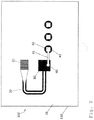
Figur 1 zeigt im Querschnitt ein nicht erfindungsgemäßes Beispiel für einoptoelektronisches Bauelement 100, das einenChip 110, vorzugsweise in Form eines SOI-Chips, aufweist. DerChip 110 umfasst einSubstrat 12 in Form eines Siliziumsubstrats, eine auf derOberseite 12a desSubstrats 12 befindlichevergrabene Siliziumdioxidschicht 11, eine auf derSiliziumdioxidschicht 11befindliche Siliziumschicht 10a und ein auf derSiliziumschicht 10abefindliches Materialschichtpaket 10. DasMaterialschichtpaket 10 bildet fachsprachlich den sogenannten "Backend of Line"-Bereich desChips 110.
In demChip 110 ist einoptischer Wellenleiter 20 integriert, bei dem es sich vorzugsweise um einen in derSiliziumschicht 10a ausgebildeten Rippenwellenleiter handelt. Außerdem ist in demChip 110, vorzugsweise in derSiliziumschicht 10a, eineelektrooptische Komponente 30 monolithisch integriert. Dieelektrooptische Komponente 30 steht mittels einerVerbindungsleitung 41 mit einem unter derSubstratrückseite 12bbefindlichen Leiterbahnanschluss 43 in Verbindung. DieVerbindungsleitung 41 erstreckt sich durch einDurchgangsloch 42 imSubstrat 12 von derelektrooptischen Komponente 30 zu dem unter derSubstratrückseite 12bbefindlichen Leiterbahnanschluss 43.
DieVerbindungsleitung 41 kann abschnittsweise auf der Chipoberseite desChips 110 aufliegen oder - wie in derFigur 1 gezeigt - innerhalb desMaterialschichtpakets 10 integriert sein. In beiden Falle erstreckt sich ein Abschnitt derVerbindungsleitung 41 vorzugsweise durch einLoch 40 imMaterialschichtpaket 10 bzw. im "Backend of Line"-Bereich desChips 110 oder durch einLoch 40 in einer oder mehreren Schichten diesesMaterialschichtpakets 10 in Richtung der Chipoberseite desChips 110. - Die
Figur 2 zeigt dasoptoelektronische Bauelement 100 gemäßFigur 1 in der Draufsicht. - Die
Figur 3 zeigt in der Draufsicht ein weiteres nicht erfindungsgemäßes Beispiel für einoptoelektronisches Bauelement 100, das einenChip 110 in Form eines SOI-Chips aufweist. In die auf der vergrabenen Siliziumdioxidschicht 11 (sieheFigur 1 )befindlichen Siliziumschicht 10a (sieheFigur 1 ) desChips 110 sind einoptischer Wellenleiter 20, einGitterkoppler 21 sowie eine elektrische Komponente in Form einerSteuerelektronik 50 monolithisch integriert. Im Übrigen gelten die obigen Ausführungen im Zusammenhang mit denFiguren 1 bis 2 entsprechend. Weitere bevorzugte Ausführungsbeispiele für optoelektronische Bauelemente sind in denFiguren 4 bis 13 gezeigt. - Die
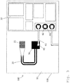
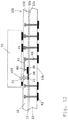
Figur 4 zeigt im Querschnitt ein nicht erfindungsgemäßes Beispiel für einoptoelektronisches Bauelement 100, das mit weiteren Komponenten auf einemVerdrahtungssubstrat 61 platziert ist und mitVergussmaterial 60 versiegelt ist. Über Anschlüsse zurelektrischen Kontaktierung 65 ist dasVerdrahtungssubstrat 61 mit demTrägersubstrat 62 verbunden. Auf demVerdrahtungssubstrat 61 befinden sich neben demoptoelektronischen Bauelement 100 ein oder mehrereelektronische Chips 63, die mit demVerdrahtungssubstrat 61 überelektrische Kontaktierungen 64 verbunden sind.
Auf der Oberseite desChips 110 im "Backend of Line"-Bereich 10 befinden sich eine oder mehrere monolithischintegrierte Linsen 23 zur optischen Kopplung der austretenden optischen Strahlung LOR eines oder mehrerer, auf demoptoelektronischen Bauelement 100befindlicher Laser 70, die überelektrische Kontaktierungen 45 mit denDurchgangslöchern 42 imChip 110 verbunden sind.
Eine oder mehrereLichtleitfasern 80 sind auf eine Weise mit auf demoptoelektronischen Bauelement 100angebrachten Steckern 81, dieUmlenkoptiken 82 enthalten, verbunden, dass die Lichtleitfaser oder -fasern 80 parallel zurChipoberseite 110 verlaufen. Die durch die Umlenkoptiken 2 umgelenkte optische Strahlung FCR wird über Umlenkeinheiten wie z.B.Gitterkoppler 21 mit einem oder mehrerenWellenleitern 20 gekoppelt und z. B. in einer monolithisch integriertenelektrooptischen Komponente 30 verarbeitet. - Die
Figur 5 zeigt im Querschnitt ein nicht erfindungsgemäßes Beispiel für einoptoelektronisches Bauelement 100 bei dem sich ein oder mehrereLaser 70 neben demoptoelektronischen Bauelement 100 auf demVerdrahtungssubstrat 61 befinden und die austretende optische Strahlung LOR durch eineLinse 24 in oder an einem oder mehrerenLasern 70 und durch die benachbarte Endfacette eines oder mehrererWellenleiter 20 in denChip 110 gekoppelt und z. B. in einer monolithisch integriertenelektrooptischen Komponente 30 verarbeitet wird. - Die
Figur 6 zeigt im Querschnitt ein nicht erfindungsgemäßes Beispiel für einoptoelektronisches Bauelement 100, bei dem die monolithisch integrierte elektrooptische Komponente einModulator 31 ist. - Die
Figur 7optoelektronische Bauelement 100 gemäßFigur 6 in der Draufsicht. - Die
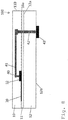
Figur 8 zeigt im Querschnitt ein nicht erfindungsgemäßes Beispiel für einoptoelektronisches Bauelement 100, bei dem die monolithisch integrierte elektrooptische Komponente einPhotodetektor 32 ist. - Die
Figur 9 zeigtdas optoelektronische Bauelement 100 gemäßFigur 8 in der Draufsicht. Die Figur 10 zeigt im Querschnitt ein nicht erfindungsgemäßes Beispiel fürein optoelektronisches Bauelement 100, bei dem eine oder mehrere Lichtleitfasern 80 auf eine Weise mit aufdem optoelektronischen Bauelement 100angebrachten Steckern 81 verbunden sind, dass die Lichtleitfaser oder -fasern 80 nahezu senkrecht inRichtung Chipoberseite 110 zeigen. Die optische Strahlung FCR wird über Umlenkeinheiten wie z.B. Gitterkoppler 21 mit einem oder mehreren Wellenleitern 20 gekoppelt und z. B. in einem passiven photonischen Bauelement 22 verarbeitet.Die Figur 11 zeigt im Querschnitt ein nicht erfindungsgemäßes Beispiel fürein optoelektronisches Bauelement 100, bei dem eine oder mehrere Lichtleitfasern 80 auf eine Weise mit aufdem optoelektronischen Bauelement 100angebrachten Steckern 81, dieUmlenkoptiken 82 enthalten, verbunden sind, dass die Lichtleitfaser oder -fasern 80parallel zur Chipoberseite 110 verlaufen. Die durch die Umlenkoptiken 2 umgelenkte optische Strahlung FCR wird über Umlenkeinheiten wie z.B. Gitterkoppler 21 mit einem oder mehreren Wellenleitern 20 gekoppelt und z. B. in einem passiven photonischen Bauelement 22 verarbeitet.Die Figur 12 zeigt im Querschnitt ein nicht erfindungsgemäßes Beispiel fürein optoelektronisches Bauelement 100, bei dem sich auf der Oberseite desChips 110 im "Backend of Line"-Bereich 10 eine oder mehrere monolithisch integrierteLinsen 23 befinden, die zur optischen Kopplung der austretenden optischen Strahlung LOR eines oder mehrerer, aufdem optoelektronischen Bauelement 100befindlicher Laser 70 dienen, die über elektrische Kontaktierungen 45mit den Durchgangslöchern 42im Chip 110 verbunden sind. Die aus der Unterseite des oder derLaser 70 austretende optische Strahlung LOR wird über Umlenkeinheiten wie z.B.Gitterkoppler 21 mit einem oder mehreren Wellenleitern 20 gekoppelt und z.B. in einer monolithisch integrierten elektrooptischen Komponente 30 verarbeitet.- Die
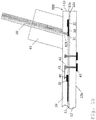
Figur 13 zeigt im Querschnitt ein nicht erfindungsgemäßes Beispiel fürein optoelektronisches Bauelement 100, bei dem sich aufdem optoelektronischen Bauelement 100 ein oder mehrereLaser 70 befinden, die über elektrische Kontaktierungen 45mit den Durchgangslöchern 42im Chip 110 verbunden sind. Die seitlich aus dem oderden Lasern 70 austretende optische Strahlung LOR wird durch eine Strahlumlenkung 27 in Umlenkeinheiten wie z.B. Gitterkoppler 21 geleitet und mit einem oder mehreren Wellenleitern 20 gekoppelt und z. B. in einer monolithisch integrierten elektrooptischen Komponente 30 verarbeitet. - Die
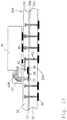
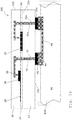
Figur 14 zeigt ein Ausführungsbeispiel für ein erfindungsgemäßes optoelektronisches Bauelement 100.Das Bauelement 100umfasst einen Chip 110mit einem Substrat 12 und mindestens einem indem Chip 110 integrierten optischen Wellenleiter 20.
- The
Figure 1 shows in cross section an example, not according to the invention, of anoptoelectronic component 100 which has achip 110, preferably in the form of an SOI chip. Thechip 110 comprises asubstrate 12 in the form of a silicon substrate, a buriedsilicon dioxide layer 11 located on theupper side 12a of thesubstrate 12, asilicon layer 10a located on thesilicon dioxide layer 11 and amaterial layer package 10 located on thesilicon layer 10a "Backend of Line" area of thechip 110.
Anoptical waveguide 20, which is preferably a rib waveguide formed in thesilicon layer 10a, is integrated in thechip 110. In addition, an electro-optical component 30 is monolithically integrated in thechip 110, preferably in thesilicon layer 10a. The electro-optical component 30 is connected by means of a connectingline 41 to aconductor track connection 43 located below the substraterear side 12b. The connectingline 41 extends through a throughhole 42 in thesubstrate 12 from the electro-optical component 30 to theconductor track connection 43 located below the substraterear side 12b.
The connectingline 41 can rest in sections on the top of thechip 110 or - as in FIGFigure 1 - be integrated within thematerial layer package 10. In both cases, a section of the connectingline 41 preferably extends through ahole 40 in thematerial layer package 10 or in the “backend of line” area of thechip 110 or through ahole 40 in one or more layers of thismaterial layer package 10 in the direction of the top side of thechip 110. - The
Figure 2 shows theoptoelectronic component 100 according toFigure 1 in top view. - The
Figure 3 FIG. 8 shows a plan view of a further example, not according to the invention, of anoptoelectronic component 100 which has achip 110 in the form of an SOI chip. In the on the buried silicon dioxide layer 11 (seeFigure 1 ) locatedsilicon layer 10a (seeFigure 1 ) of thechip 110, anoptical waveguide 20, agrating coupler 21 and an electrical component in the form ofcontrol electronics 50 are monolithically integrated. Otherwise, the above statements apply in connection with theFigures 1 to 2 corresponding. Further preferred exemplary embodiments for optoelectronic components are shown in FIGSFigures 4 to 13 shown. - The
Figure 4 FIG. 8 shows in cross section an example, not according to the invention, for anoptoelectronic component 100 which is placed with further components on awiring substrate 61 and is sealed withpotting material 60. Thewiring substrate 61 is connected to thecarrier substrate 62 via connections for electrical contacting 65. On thewiring substrate 61, in addition to theoptoelectronic component 100, there are one or moreelectronic chips 63 which are connected to thewiring substrate 61 viaelectrical contacts 64.
On the top of thechip 110 in the "backend of line"area 10 there are one or more monolithicallyintegrated lenses 23 for optically coupling the emerging optical radiation LOR of one ormore lasers 70 located on theoptoelectronic component 100, which viaelectrical contacts 45 are connected to the throughholes 42 in thechip 110.
One or moreoptical fibers 80 are connected in such a way to plugs 81, which are attached to theoptoelectronic component 100 and contain deflectingoptics 82, that the optical fibers orfibers 80 run parallel to thetop side 110 of the chip. The optical radiation FCR deflected by the deflection optics 2 is coupled to one ormore waveguides 20 via deflection units such asgrating couplers 21 and z. B. processed in a monolithically integrated electro-optical component 30. - The
Figure 5 shows in cross section an example not according to the invention for anoptoelectronic component 100 in which one ormore lasers 70 are next to theoptoelectronic component 100 on thewiring substrate 61 and the emerging optical radiation LOR through alens 24 in or on one ormore lasers 70 and through the adjacent end facet of one ormore waveguides 20 is coupled into thechip 110 and z. B. is processed in a monolithically integrated electro-optical component 30. - The
Figure 6 shows in cross section an example, not according to the invention, of anoptoelectronic component 100 in which the monolithically integrated electro-optical component is amodulator 31. - The
Figure 7 shows theoptoelectronic component 100 according toFigure 6 in top view. - The
Figure 8 shows in cross section an example, not according to the invention, of anoptoelectronic component 100 in which the monolithically integrated electro-optical component is aphotodetector 32. - The
Figure 9 shows theoptoelectronic component 100 according toFigure 8 in top view. - The
Figure 10 shows in cross section an example not according to the invention for anoptoelectronic component 100, in which one or moreoptical fibers 80 are connected toplugs 81 attached to theoptoelectronic component 100 in such a way that the optical fibers orfibers 80 point almost perpendicularly in the direction of thechip top 110. The optical radiation FCR is deflected via deflection units such.B. grating coupler 21 coupled to one ormore waveguides 20 and z. B. processed in apassive photonic component 22. - The
Figure 11 shows in cross section an example of anoptoelectronic component 100, not according to the invention, in which one or moreoptical fibers 80 are connected in such a way to plugs 81 which are attached to theoptoelectronic component 100 and contain deflectingoptics 82 that the optical fiber orfibers 80 are parallel to the Chip top 110 run. The deflected by the deflecting optics 2 optical radiation FCR is deflected via deflection units such.B. grating coupler 21 coupled to one ormore waveguides 20 and z. B. processed in apassive photonic component 22. - The
Figure 12 shows in cross section an example not according to the invention for anoptoelectronic component 100, in which one or more monolithicallyintegrated lenses 23 are located on the top of thechip 110 in the "backend of line"area 10, which are used for optical coupling of the emerging optical radiation LOR or a plurality oflasers 70 located onoptoelectronic component 100, which are connected to throughholes 42 inchip 110 viaelectrical contacts 45. The optical radiation LOR emerging from the underside of the laser (s) 70 is coupled to one ormore waveguides 20 via deflection units such asgrating couplers 21 and processed, for example, in a monolithically integrated electro-optical component 30. - The
Figure 13 FIG. 12 shows in cross section an example, not according to the invention, of anoptoelectronic component 100 in which one ormore lasers 70 are located onoptoelectronic component 100 and are connected to throughholes 42 inchip 110 viaelectrical contacts 45. The optical radiation LOR emerging from the side of the laser orlasers 70 is deflected by abeam deflector 27 in deflection units such as e.g.B. grating coupler 21 and coupled to one ormore waveguides 20 and z. B. processed in a monolithically integrated electro-optical component 30. - The
Figure 14 FIG. 3 shows an exemplary embodiment of anoptoelectronic component 100 according to the invention. Thecomponent 100 comprises achip 110 with asubstrate 12 and at least oneoptical waveguide 20 integrated in thechip 110.
In einer oder mehreren auf der Substratoberseite 12a des Substrats 12 angeordneten Halbleiterschichten des Chips 110 oder auf der Substratoberseite 12a des Substrats 12 ist eine elektrooptische Komponente 30 monolithisch integriert.An electro-
Zumindest ein elektrischer Anschluss der monolithisch integrierten elektrooptischen Komponente 30 steht mittels einer Verbindungsleitung 41 mit einem unter der Substratrückseite 12b befindlichen Leiterbahnanschluss 43 in Verbindung.At least one electrical connection of the monolithically integrated electro-
Die Verbindungsleitung 41 erstreckt sich durch ein Durchgangsloch 42 im Substrat 12 von der elektrooptischen Komponente 30 zu dem unter der Substratrückseite 12b befindlichen Leiterbahnanschluss 43.The connecting
In einer oder mehreren auf der Substratoberseite 12a des Substrats 12 angeordneten Halbleiterschichten des Chips 110 oder auf der Substratoberseite 12a des Substrats 12 ist außerdem eine elektrische Komponente 50 monolithisch integriert.An
Zumindest ein elektrischer Anschluss der monolithisch integrierten elektrischen Komponente 50 steht mittels einer Verbindungsleitung 41a mit einem unter der Substratrückseite 12b befindlichen Leiterbahnanschluss 43a in Verbindung.At least one electrical connection of the monolithically integrated
Die Verbindungsleitung 41a erstreckt sich durch ein Durchgangsloch 42a im Substrat 12 von der elektrischen Komponente 50 zu dem unter der Substratrückseite 12b befindlichen Leiterbahnanschluss 43a.The connecting
Der Chip 110 ist mit seiner Unterseite auf einer Leiterplatte 610 aufgesetzt, die eine Verdrahtungsebene für die auf der Chiprückseite bzw. der Substratrückseite 12b befindlichen elektrischen Leiterbahnanschlüsse 43 und 43a bildet. Die Leiterplatte 610 weist zumindest eine Verbindungsleitung 46 auf, die den mit der elektrischen Komponente 50 verbundenen Leiterbahnanschluss 43a und den mit der elektrooptischen Komponente 30 verbundenen Leiterbahnanschluss 43 miteinander elektrisch verbindet.The lower side of the
Die
In einer oder mehreren auf der Substratoberseite 12a des Substrats 12 angeordneten Halbleiterschichten des Chips 110 oder auf der Substratoberseite 12a des Substrats 12 sind eine elektrooptische Komponente 30 und eine elektrische Komponente 50 monolithisch integriert.An electro-
Zumindest ein elektrischer Anschluss der monolithisch integrierten elektrischen Komponente 50 steht mittels einer Verbindungsleitung 41a mit einem unter der Substratrückseite 12b befindlichen Leiterbahnanschluss 43a in Verbindung.At least one electrical connection of the monolithically integrated
Die Verbindungsleitung 41a erstreckt sich durch ein Durchgangsloch 42a im Substrat 12 von der elektrischen Komponente 50 zu dem unter der Substratrückseite 12b befindlichen Leiterbahnanschluss 43a.The connecting
Der Chip 110 ist mit seiner Unterseite auf einer Leiterplatte 610 aufgesetzt, die eine Verdrahtungsebene für den auf der Chiprückseite bzw. der Substratrückseite 12b befindlichen elektrischen Leiterbahnanschluss 43a bildet.The lower side of the
Die Leiterplatte 610 weist zumindest eine Verbindungsleitung 46 auf, die den mit der elektrischen Komponente 50 verbundenen Leiterbahnanschluss 43a mit einer anderen, aus Gründen der Übersicht in der
Die elektrooptische Komponente 30 und die elektrische Komponente 50 sind mittels mindestens einer Leitung 620 verbunden, die auf der Substratoberseite 12a des Substrats 12 angeordnet ist.The electro-
Bei den Bauelementen gemäß den
Die Bauelemente gemäß den
Obwohl die Erfindung im Detail durch bevorzugte Ausführungsbeispiele näher illustriert und beschrieben wurde, so ist die Erfindung nicht durch die offenbarten Beispiele eingeschränkt, sondern allein durch den Umfang der Ansprüche.Although the invention has been illustrated and described in more detail by means of preferred exemplary embodiments, the invention is not represented by the examples disclosed limited only by the scope of the claims.
- [1] H. Schröder, T. Bierhoff, and D. Craiovan, "Anforderungen und Lösungen zur hochpräzisen optoelektronischen und mikrooptischen Montage auf Baugruppenträgern," Cooperative Computing & Communication Laboratory, C-Lab Report 9, 6, 2010.[1] H. Schröder, T. Bierhoff, and D. Craiovan, "Requirements and solutions for high-precision optoelectronic and micro-optical assembly on subracks," Cooperative Computing & Communication Laboratory, C-Lab Report 9, 6, 2010.
-
[2]
F. E. Doany, B. G. Lee, C. L. Schow, C. K. Tsang, C. Baks, Y. Kwark, R. John, J. U. Knickerbocker, and J. A. Kash, "Terabit/s-class 24-channel bidirectional optical transceiver module based on TSV Si carrier for boardlevel interconnects," in ECTC, Electronic Components and Technology Conference, Piscataway, NJ: IEEE, 2010, pp. 58-65 FE Doany, BG Lee, CL Schow, CK Tsang, C. Baks, Y. Kwark, R. John, JU Knickerbocker, and JA Kash, "Terabit / s-class 24-channel bidirectional optical transceiver module based on TSV Si carrier for boardlevel interconnects, "in ECTC, Electronic Components and Technology Conference, Piscataway, NJ: IEEE, 2010, pp. 58-65 -
[3] P. de Dobbelaere, G. Young, and M. Peterson, "Method And System For A Photonic Interposer",
USA 13/422,776, July 12, 2012 USA 13 / 422,776, July 12, 2012
- 1010
- MaterialschichtpaketMaterial layer package
- 10a10a
- SiliziumschichtSilicon layer
- 1111
- SiliziumdioxidschichtSilicon dioxide layer
- 1212
- SubstratSubstrate
- 12a12a
- Oberseite des SubstratsTop of the substrate
- 12b12b
- SubstratrückseiteSubstrate back
- 2020th
- optischer Wellenleiteroptical waveguide
- 2121st
- GitterkopplerGrating coupler
- 2222nd
- passives photonisches Bauelementpassive photonic component
- 2323
- monolithisch integrierte Linse im "Backend of Line"-Bereichmonolithically integrated lens in the "backend of line" area
- 2424
- Linse in oder an einem LaserLens in or on a laser
- 2727
- StrahlumlenkungBeam deflection
- 3030th
- monolithisch integrierte elektrooptische Komponentemonolithically integrated electro-optical component
- 3131
- monolithisch integrierter elektrooptischer Modulatormonolithically integrated electro-optical modulator
- 3232
- monolithisch integrierte Photodiode / Photodetektormonolithically integrated photodiode / photodetector
- 4040
- Lochhole
- 4141
- VerbindungsleitungConnecting line
- 41a41a
- VerbindungsleitungConnecting line
- 4242
- DurchgangslochThrough hole
- 42a42a
- DurchgangslochThrough hole
- 4343
- LeiterbahnanschlussTrack connection
- 43a43a
- LeiterbahnanschlussTrack connection
- 4444
- Anschluss zur elektrischen Kontaktierung auf einem VerdrahtungssubstratConnection for electrical contacting on a wiring substrate
- 4545
- Anschluss zur elektrischen Kontaktierung eines LaserchipsConnection for making electrical contact with a laser chip
- 4646
- VerbindungsleitungConnecting line
- 5050
- monolithisch integrierte Steuerelektronik (Kointegration)monolithically integrated control electronics (cointegration)
- 6060
- VergussmaterialPotting material
- 6161
- VerdrahtungssubstratWiring substrate
- 6262
- Trägersubstrat (z. B. PCB Platine)Carrier substrate (e.g. PCB circuit board)
- 6363
- elektronischer Chipelectronic chip
- 6464
- Anschluss zur elektrischen Kontaktierung eines elektronischen Chips mit dem VerdrahtungssubstratConnection for making electrical contact between an electronic chip and the wiring substrate
- 6565
- Anschluss zur elektrischen Kontaktierung des Verdrahtungssubstrats mit dem TrägersubstratConnection for making electrical contact between the wiring substrate and the carrier substrate
- 7070
- Laserlaser
- 8080
- Faserfiber
- 8181
- FasersteckerFiber connector
- 8282
- Umlenkoptik im FasersteckerDeflection optics in the fiber connector
- 100100
- optoelektronisches Bauelementoptoelectronic component
- 110110
- Chipchip
- 610610
- LeiterplatteCircuit board
- 620620
- Leitungmanagement
Claims (12)
- Optoelectronic component (100) comprising a chip (110)- comprising a substrate (12) and- at least one optical waveguide (20) integrated in the chip (110),
wherein- an electro-optical component (30) is monolithically integrated in one or a plurality of semiconductor layers of the chip (110) arranged on the substrate top side (12a) of the substrate (12), or on the substrate top side (12a) of the substrate (12) and- at least one electrical connection of the monolithically integrated electro-optical component (30) is connected by means of a first connection line (41) to a first conductor track connection (43) situated below the substrate rear side (12b),- wherein the first connection line (41) extends through a through hole (42) in the substrate (12) from the electro-optical component (30) to the first conductor track connection (43) situated below the substrate rear side (12b),
characterized in that- an electrical component (50) is monolithically integrated in one or a plurality of semiconductor layers of the chip (110) arranged on the substrate top side (12a) of the substrate (12) or on the substrate top side (12a) of the substrate (12),- at least one electrical connection of the monolithically integrated electrical component (50) is connected by means of a second connection line (41a) to a second conductor track connection (43a) situated below the substrate rear side (12b),- the chip (110) is placed by its underside on a printed circuit board (610) that forms a wiring plane for the electrical conductor track connections (43, 43a) situated on the substrate rear side (12b), and- the printed circuit board (610) has at least one third connection line (46) which electrically interconnects the second conductor track connection (43a) and the first conductor track connection (43). - Optoelectronic component (100) according to Claim 1,
characterized in that- at least one optical connection, preferably all of the optical connections, are arranged on the chip top side of the chip (110) and- at least one of the electrical connections, preferably all of the electrical connections, are arranged on the chip underside of the chip (110). - Optoelectronic component (100) according to either of the preceding claims,
characterized in that
the monolithically integrated electro-optical component (30) is a photodetector (32) or a modulator (31) . - Optoelectronic component (100) according to any of the preceding claims,
characterized in that
the integrated waveguide (20) is equipped with or connected to a deflection device which deflects optical radiation to be coupled out from the waveguide (20) virtually perpendicularly in the direction of the chip top side, or deflects radiation incident virtually perpendicularly from the chip top side and couples it into the waveguide (20) . - Optoelectronic component (100) according to Claim 4,
characterized in that
the deflection device is formed by a grating coupler (21) embodied in the waveguide (20). - Optoelectronic component (100) according to any of the preceding claims,
characterized in that- a silicon dioxide layer is situated on the substrate (12) and a silicon layer (10a) is situated above said silicon dioxide layer, and- the optical waveguide (20) and the electro-optical component (30) are monolithically integrated in the silicon layer (10a). - Optoelectronic component (100) according to any of the preceding claims,
characterized in that
the monolithically integrated electrical component (50) is an amplifier or a driver. - Optoelectronic component (100) according to any of the preceding claims,
characterized in that
the at least one integrated waveguide (20) or at least one of the integrated waveguides (20)- in the region of one of its waveguide ends is equipped with or connected to a deflection device by which optical radiation that comes from a light source arranged on the chip top side of the chip (110) and is incident virtually perpendicularly to the chip top side is coupled into the waveguide (20), and- in the region of the other waveguide end is equipped with or connected to a deflection device which deflects optical radiation to be coupled out from the waveguide (20) virtually perpendicularly in the direction of the chip top side, in particular in the direction of an optical fibre arranged on the chip top side or in the direction of a light deflection element arranged on the chip top side,- wherein at least one electrical connection of the light source is connected by means of a connection line to a conductor track connection situated below the substrate rear side (12b). - Optoelectronic component (100) according to Claim 8,
characterized in that
a modulator is monolithically integrated between the two waveguide ends in the chip (110), said modulator modulating the radiation of the light source before coupling into the optical fibre. - Optoelectronic component (100) according to any of the preceding claims,
characterized in that
the at least one integrated waveguide (20) or at least one of the integrated waveguides (20)- in the region of one of its waveguide ends is equipped with or connected to a deflection device by which optical radiation that comes from an optical fibre arranged on the chip top side and is incident virtually perpendicularly to the chip top side is coupled into the waveguide (20), and- in the region of the other waveguide end is connected to a photodetector (32) integrated in the chip (110). - Optoelectronic component (100) according to Claim 10,
characterized in that
a transimpedance amplifier is monolithically integrated in the chip (110), said transimpedance amplifier amplifying the electrical signal of the photodetector (32). - Optoelectronic component (100) according to any of the preceding claims,
characterized in that- the electro-optical component (30) and the electrical component (50) are connected by means of a line (620) that is arranged on the substrate top side (12a) of the substrate (12).
Applications Claiming Priority (2)
| Application Number | Priority Date | Filing Date | Title |
|---|---|---|---|
| DE102014219792.9A DE102014219792A1 (en) | 2014-09-30 | 2014-09-30 | Optoelectronic component |
| PCT/DE2015/200464 WO2016050243A1 (en) | 2014-09-30 | 2015-09-28 | Optoelectronic component |
Publications (2)
| Publication Number | Publication Date |
|---|---|
| EP3201663A1 EP3201663A1 (en) | 2017-08-09 |
| EP3201663B1 true EP3201663B1 (en) | 2021-01-06 |
Family
ID=54883942
Family Applications (1)
| Application Number | Title | Priority Date | Filing Date |
|---|---|---|---|
| EP15812943.7A Active EP3201663B1 (en) | 2014-09-30 | 2015-09-28 | Optoelectronic component |
Country Status (5)
| Country | Link |
|---|---|
| US (1) | US10775561B2 (en) |
| EP (1) | EP3201663B1 (en) |
| CN (1) | CN106716199B (en) |
| DE (2) | DE102014219792A1 (en) |
| WO (1) | WO2016050243A1 (en) |
Families Citing this family (12)
| Publication number | Priority date | Publication date | Assignee | Title |
|---|---|---|---|---|
| US10976491B2 (en) * | 2016-11-23 | 2021-04-13 | The Research Foundation For The State University Of New York | Photonics interposer optoelectronics |
| TWI686943B (en) * | 2016-11-23 | 2020-03-01 | 紐約州立大學研究基金會 | Photonics interposer optoelectronics |
| US10698156B2 (en) | 2017-04-27 | 2020-06-30 | The Research Foundation For The State University Of New York | Wafer scale bonded active photonics interposer |
| US11315878B2 (en) * | 2018-10-31 | 2022-04-26 | Taiwan Semiconductor Manufacturing Company, Ltd. | Photonics integrated circuit package |
| CN110596830A (en) * | 2019-09-24 | 2019-12-20 | 武汉光迅科技股份有限公司 | Optical assembly |
| US20210096311A1 (en) * | 2019-09-27 | 2021-04-01 | Taiwan Semiconductor Manufacturing Co., Ltd. | Photonic semiconductor device and method of manufacture |
| US11076491B2 (en) * | 2019-10-16 | 2021-07-27 | Compass Technology Company Limited | Integrated electro-optical flexible circuit board |
| CN114788018A (en) * | 2019-12-19 | 2022-07-22 | 电光-Ic股份有限公司 | Optical receiver including monolithically integrated photodiode and transimpedance amplifier |
| US11513285B2 (en) * | 2020-01-08 | 2022-11-29 | Avicenatech Corp. | Packaging for microLEDs for chip to chip communication |
| US11609391B2 (en) * | 2020-05-19 | 2023-03-21 | Taiwan Semiconductor Manufacturing Company, Ltd. | Semiconductor package and manufacturing method thereof |
| CA3119015A1 (en) * | 2020-05-22 | 2021-11-22 | Ranovus Inc. | Carrier based laser assembly and method of assembly thereof with photonic integrated circuit |
| CN115867831A (en) * | 2020-07-20 | 2023-03-28 | 应用材料公司 | Integrated conductive vias for optical devices |
Family Cites Families (20)
| Publication number | Priority date | Publication date | Assignee | Title |
|---|---|---|---|---|
| FR2835095B1 (en) * | 2002-01-22 | 2005-03-18 | PROCESS FOR PREPARING SEPARABLE SEMICONDUCTOR ASSEMBLIES, IN PARTICULAR FOR FORMING SUBSTRATES FOR ELECTRONICS, OPTOELECTRIC, AND OPTICS | |
| FI20031796A (en) * | 2003-12-09 | 2005-06-10 | Asperation Oy | A method of constructing an EMI shield around a component to be embedded in a circuit board |
| US8168939B2 (en) | 2008-07-09 | 2012-05-01 | Luxtera, Inc. | Method and system for a light source assembly supporting direct coupling to an integrated circuit |
| US8831437B2 (en) * | 2009-09-04 | 2014-09-09 | Luxtera, Inc. | Method and system for a photonic interposer |
| US8213751B1 (en) * | 2008-11-26 | 2012-07-03 | Optonet Inc. | Electronic-integration compatible photonic integrated circuit and method for fabricating electronic-integration compatible photonic integrated circuit |
| US9331096B2 (en) * | 2009-09-04 | 2016-05-03 | Luxtera, Inc. | Method and system for hybrid integration of optical communication systems |
| GB0915775D0 (en) | 2009-09-09 | 2009-10-07 | Univ Gent | Implantable sensor |
| US8803269B2 (en) * | 2011-05-05 | 2014-08-12 | Cisco Technology, Inc. | Wafer scale packaging platform for transceivers |
| WO2013086047A1 (en) * | 2011-12-06 | 2013-06-13 | Cornell University | Integrated multi-chip module optical interconnect platform |
| US9423560B2 (en) | 2011-12-15 | 2016-08-23 | Alcatel Lucent | Electronic/photonic integrated circuit architecture and method of manufacture thereof |
| WO2013101184A1 (en) * | 2011-12-30 | 2013-07-04 | Intel Corporation | Optical i/o system using planar light-wave integrated circuit |
| TWI502689B (en) | 2012-03-16 | 2015-10-01 | Luxtera Inc | Method and system for a photonic interposer |
| KR20140146612A (en) * | 2012-04-16 | 2014-12-26 | 휴렛-팩커드 디벨롭먼트 컴퍼니, 엘.피. | Integrated optical sub-assembly |
| JP2014035546A (en) | 2012-08-07 | 2014-02-24 | Luxtera Inc | Method and system for hybrid integration of optical communication system |
| US9057450B2 (en) * | 2013-03-13 | 2015-06-16 | Elliott Company | Valve exerciser for an emergency shutoff valve of a steam turbine and method for using the same |
| US20140270629A1 (en) * | 2013-03-15 | 2014-09-18 | Apic Corporation | Optical waveguide network of an interconnecting ic module |
| US9091819B2 (en) * | 2013-04-11 | 2015-07-28 | International Business Machines Corporation | Grating edge coupler and method of forming same |
| US9952456B2 (en) * | 2013-06-09 | 2018-04-24 | Electronic Photonic Ic Inc. (Epic Inc.) | Thin layer photonic integrated circuit based optical signal manipulators |
| US10606003B2 (en) * | 2013-08-02 | 2020-03-31 | Luxtera, Inc. | Method and system for an optical coupler for silicon photonics devices |
| DE102014219663A1 (en) | 2014-09-29 | 2016-03-31 | Ihp Gmbh - Innovations For High Performance Microelectronics / Leibniz-Institut Für Innovative Mikroelektronik | Photonically integrated chip, optical component with photonically integrated chip and method for its production |
-
2014
- 2014-09-30 DE DE102014219792.9A patent/DE102014219792A1/en not_active Withdrawn
-
2015
- 2015-09-28 US US15/515,923 patent/US10775561B2/en active Active
- 2015-09-28 CN CN201580049634.9A patent/CN106716199B/en active Active
- 2015-09-28 EP EP15812943.7A patent/EP3201663B1/en active Active
- 2015-09-28 WO PCT/DE2015/200464 patent/WO2016050243A1/en active Application Filing
- 2015-09-28 DE DE112015004474.4T patent/DE112015004474A5/en not_active Withdrawn
Non-Patent Citations (1)
| Title |
|---|
| KNOLL D ET AL: "Monolithically integrated 25Gbit/sec receiver for 1.55[mu]m in photonic BiCMOS technology", OFC 2014, OSA, 9 March 2014 (2014-03-09), pages 1 - 3, XP032632948, DOI: 10.1109/OFC.2014.6886828 * |
Also Published As
| Publication number | Publication date |
|---|---|
| CN106716199A (en) | 2017-05-24 |
| CN106716199B (en) | 2020-02-28 |
| WO2016050243A1 (en) | 2016-04-07 |
| US10775561B2 (en) | 2020-09-15 |
| US20190146151A1 (en) | 2019-05-16 |
| DE102014219792A1 (en) | 2016-03-31 |
| DE112015004474A5 (en) | 2017-06-14 |
| EP3201663A1 (en) | 2017-08-09 |
Similar Documents
| Publication | Publication Date | Title |
|---|---|---|
| EP3201663B1 (en) | Optoelectronic component | |
| DE60208416T2 (en) | Digital Optic Network Architecture | |
| DE69836058T2 (en) | Multi-channel optical receiver / transmitter system | |
| EP0383138A2 (en) | Device for the direct optical reception of a plurality of wave lengths | |
| DE102014101671B4 (en) | Bidirectional dual-wavelength optical communication system and method for communicating optical signals | |
| US7876984B2 (en) | Planar optical waveguide array module and method of fabricating the same | |
| DE10150401A1 (en) | Optoelectronic component has solder connections between metallisation structures of optical component system and optical lens system | |
| JPWO2006035499A1 (en) | Opto-electric integrated circuit element and transmission device using the same | |
| DE60219161T2 (en) | INTEGRATION OF OPTOELECTRONIC COMPONENTS | |
| DE112008001441B4 (en) | Optical connection | |
| DE4106721C2 (en) | ||
| EP2200194B1 (en) | Detector module | |
| DE102004025659A1 (en) | Optoelectric transmission module and method for its production | |
| DE10213599A1 (en) | Waveguide receiver with a post-amplifier with adjustable bandwidth | |
| EP0440087B1 (en) | Optical signal connecting device for plugs of a plug cabinet | |
| DE102019117629A1 (en) | INTEGRATION PHOTONIK PACKAGE | |
| DE10196455B4 (en) | Module for optical signal transmission | |
| JP5800466B2 (en) | Multi-channel optical transmission module | |
| EP0442312A2 (en) | Integrated optical transmitter and/or receiver | |
| DE202015106860U1 (en) | Optical multi-channel transmitting and / or receiving module, in particular for high bit rate digital optical signals | |
| DE102005062735B4 (en) | Electro-optical assembly for multiplexing or demultiplexing an optical signal | |
| DE10160508B4 (en) | Arrangement for detecting optical signals of at least one optical channel of a planar optical circuit and / or for coupling optical signals into at least one optical channel of a planar optical circuit | |
| WO2004025341A1 (en) | Printed circuit board comprising electrical conductor paths and means for electro-optical and/or opto-electrical conversion | |
| DE10319900A1 (en) | Optoelectronic transmission and / or reception arrangement | |
| CN107209335B (en) | Electronic/photonic chip integration and bonding |
Legal Events
| Date | Code | Title | Description |
|---|---|---|---|
| STAA | Information on the status of an ep patent application or granted ep patent |
Free format text: STATUS: THE INTERNATIONAL PUBLICATION HAS BEEN MADE |
|
| PUAI | Public reference made under article 153(3) epc to a published international application that has entered the european phase |
Free format text: ORIGINAL CODE: 0009012 |
|
| STAA | Information on the status of an ep patent application or granted ep patent |
Free format text: STATUS: REQUEST FOR EXAMINATION WAS MADE |
|
| 17P | Request for examination filed |
Effective date: 20170428 |
|
| AK | Designated contracting states |
Kind code of ref document: A1 Designated state(s): AL AT BE BG CH CY CZ DE DK EE ES FI FR GB GR HR HU IE IS IT LI LT LU LV MC MK MT NL NO PL PT RO RS SE SI SK SM TR |
|
| AX | Request for extension of the european patent |
Extension state: BA ME |
|
| DAV | Request for validation of the european patent (deleted) | ||
| DAX | Request for extension of the european patent (deleted) | ||
| STAA | Information on the status of an ep patent application or granted ep patent |
Free format text: STATUS: EXAMINATION IS IN PROGRESS |
|
| 17Q | First examination report despatched |
Effective date: 20190104 |
|
| GRAP | Despatch of communication of intention to grant a patent |
Free format text: ORIGINAL CODE: EPIDOSNIGR1 |
|
| STAA | Information on the status of an ep patent application or granted ep patent |
Free format text: STATUS: GRANT OF PATENT IS INTENDED |
|
| INTG | Intention to grant announced |
Effective date: 20200806 |
|
| GRAS | Grant fee paid |
Free format text: ORIGINAL CODE: EPIDOSNIGR3 |
|
| GRAA | (expected) grant |
Free format text: ORIGINAL CODE: 0009210 |
|
| STAA | Information on the status of an ep patent application or granted ep patent |
Free format text: STATUS: THE PATENT HAS BEEN GRANTED |
|
| AK | Designated contracting states |
Kind code of ref document: B1 Designated state(s): AL AT BE BG CH CY CZ DE DK EE ES FI FR GB GR HR HU IE IS IT LI LT LU LV MC MK MT NL NO PL PT RO RS SE SI SK SM TR |
|
| REG | Reference to a national code |
Ref country code: GB Ref legal event code: FG4D |
|
| REG | Reference to a national code |
Ref country code: AT Ref legal event code: REF Ref document number: 1352989 Country of ref document: AT Kind code of ref document: T Effective date: 20210115 Ref country code: CH Ref legal event code: EP |
|
| REG | Reference to a national code |
Ref country code: DE Ref legal event code: R096 Ref document number: 502015014133 Country of ref document: DE |
|
| REG | Reference to a national code |
Ref country code: IE Ref legal event code: FG4D Free format text: LANGUAGE OF EP DOCUMENT: GERMAN |
|
| REG | Reference to a national code |
Ref country code: NL Ref legal event code: FP |
|
| RAP2 | Party data changed (patent owner data changed or rights of a patent transferred) |
Owner name: SICOYA GMBH |
|
| REG | Reference to a national code |
Ref country code: LT Ref legal event code: MG9D |
|
| PG25 | Lapsed in a contracting state [announced via postgrant information from national office to epo] |
Ref country code: LT Free format text: LAPSE BECAUSE OF FAILURE TO SUBMIT A TRANSLATION OF THE DESCRIPTION OR TO PAY THE FEE WITHIN THE PRESCRIBED TIME-LIMIT Effective date: 20210106 Ref country code: PT Free format text: LAPSE BECAUSE OF FAILURE TO SUBMIT A TRANSLATION OF THE DESCRIPTION OR TO PAY THE FEE WITHIN THE PRESCRIBED TIME-LIMIT Effective date: 20210506 Ref country code: NO Free format text: LAPSE BECAUSE OF FAILURE TO SUBMIT A TRANSLATION OF THE DESCRIPTION OR TO PAY THE FEE WITHIN THE PRESCRIBED TIME-LIMIT Effective date: 20210406 Ref country code: HR Free format text: LAPSE BECAUSE OF FAILURE TO SUBMIT A TRANSLATION OF THE DESCRIPTION OR TO PAY THE FEE WITHIN THE PRESCRIBED TIME-LIMIT Effective date: 20210106 Ref country code: GR Free format text: LAPSE BECAUSE OF FAILURE TO SUBMIT A TRANSLATION OF THE DESCRIPTION OR TO PAY THE FEE WITHIN THE PRESCRIBED TIME-LIMIT Effective date: 20210407 Ref country code: FI Free format text: LAPSE BECAUSE OF FAILURE TO SUBMIT A TRANSLATION OF THE DESCRIPTION OR TO PAY THE FEE WITHIN THE PRESCRIBED TIME-LIMIT Effective date: 20210106 Ref country code: BG Free format text: LAPSE BECAUSE OF FAILURE TO SUBMIT A TRANSLATION OF THE DESCRIPTION OR TO PAY THE FEE WITHIN THE PRESCRIBED TIME-LIMIT Effective date: 20210406 |
|
| REG | Reference to a national code |
Ref country code: DE Ref legal event code: R081 Ref document number: 502015014133 Country of ref document: DE Owner name: SICOYA GMBH, DE Free format text: FORMER OWNER: TECHNISCHE UNIVERSITAET BERLIN, 10623 BERLIN, DE |
|
| PG25 | Lapsed in a contracting state [announced via postgrant information from national office to epo] |
Ref country code: SE Free format text: LAPSE BECAUSE OF FAILURE TO SUBMIT A TRANSLATION OF THE DESCRIPTION OR TO PAY THE FEE WITHIN THE PRESCRIBED TIME-LIMIT Effective date: 20210106 Ref country code: PL Free format text: LAPSE BECAUSE OF FAILURE TO SUBMIT A TRANSLATION OF THE DESCRIPTION OR TO PAY THE FEE WITHIN THE PRESCRIBED TIME-LIMIT Effective date: 20210106 Ref country code: LV Free format text: LAPSE BECAUSE OF FAILURE TO SUBMIT A TRANSLATION OF THE DESCRIPTION OR TO PAY THE FEE WITHIN THE PRESCRIBED TIME-LIMIT Effective date: 20210106 Ref country code: RS Free format text: LAPSE BECAUSE OF FAILURE TO SUBMIT A TRANSLATION OF THE DESCRIPTION OR TO PAY THE FEE WITHIN THE PRESCRIBED TIME-LIMIT Effective date: 20210106 |
|
| PG25 | Lapsed in a contracting state [announced via postgrant information from national office to epo] |
Ref country code: IS Free format text: LAPSE BECAUSE OF FAILURE TO SUBMIT A TRANSLATION OF THE DESCRIPTION OR TO PAY THE FEE WITHIN THE PRESCRIBED TIME-LIMIT Effective date: 20210506 |
|
| REG | Reference to a national code |
Ref country code: DE Ref legal event code: R097 Ref document number: 502015014133 Country of ref document: DE |
|
| REG | Reference to a national code |
Ref country code: GB Ref legal event code: 732E Free format text: REGISTERED BETWEEN 20210923 AND 20210929 |
|
| PG25 | Lapsed in a contracting state [announced via postgrant information from national office to epo] |
Ref country code: CZ Free format text: LAPSE BECAUSE OF FAILURE TO SUBMIT A TRANSLATION OF THE DESCRIPTION OR TO PAY THE FEE WITHIN THE PRESCRIBED TIME-LIMIT Effective date: 20210106 Ref country code: EE Free format text: LAPSE BECAUSE OF FAILURE TO SUBMIT A TRANSLATION OF THE DESCRIPTION OR TO PAY THE FEE WITHIN THE PRESCRIBED TIME-LIMIT Effective date: 20210106 Ref country code: SM Free format text: LAPSE BECAUSE OF FAILURE TO SUBMIT A TRANSLATION OF THE DESCRIPTION OR TO PAY THE FEE WITHIN THE PRESCRIBED TIME-LIMIT Effective date: 20210106 |
|
| PLBE | No opposition filed within time limit |
Free format text: ORIGINAL CODE: 0009261 |
|
| STAA | Information on the status of an ep patent application or granted ep patent |
Free format text: STATUS: NO OPPOSITION FILED WITHIN TIME LIMIT |
|
| PG25 | Lapsed in a contracting state [announced via postgrant information from national office to epo] |
Ref country code: SK Free format text: LAPSE BECAUSE OF FAILURE TO SUBMIT A TRANSLATION OF THE DESCRIPTION OR TO PAY THE FEE WITHIN THE PRESCRIBED TIME-LIMIT Effective date: 20210106 Ref country code: DK Free format text: LAPSE BECAUSE OF FAILURE TO SUBMIT A TRANSLATION OF THE DESCRIPTION OR TO PAY THE FEE WITHIN THE PRESCRIBED TIME-LIMIT Effective date: 20210106 Ref country code: RO Free format text: LAPSE BECAUSE OF FAILURE TO SUBMIT A TRANSLATION OF THE DESCRIPTION OR TO PAY THE FEE WITHIN THE PRESCRIBED TIME-LIMIT Effective date: 20210106 |
|
| 26N | No opposition filed |
Effective date: 20211007 |
|
| REG | Reference to a national code |
Ref country code: NL Ref legal event code: PD Owner name: SICOYA GMBH; DE Free format text: DETAILS ASSIGNMENT: CHANGE OF OWNER(S), ASSIGNMENT; FORMER OWNER NAME: TECHNISCHE UNIVERSITAET BERLIN Effective date: 20211123 |
|
| REG | Reference to a national code |
Ref country code: BE Ref legal event code: PD Owner name: SICOYA GMBH; DE Free format text: DETAILS ASSIGNMENT: CHANGE OF OWNER(S), ASSIGNMENT; FORMER OWNER NAME: TECHNISCHE UNIVERSITAET BERLIN Effective date: 20211104 |
|
| PG25 | Lapsed in a contracting state [announced via postgrant information from national office to epo] |
Ref country code: AL Free format text: LAPSE BECAUSE OF FAILURE TO SUBMIT A TRANSLATION OF THE DESCRIPTION OR TO PAY THE FEE WITHIN THE PRESCRIBED TIME-LIMIT Effective date: 20210106 Ref country code: ES Free format text: LAPSE BECAUSE OF FAILURE TO SUBMIT A TRANSLATION OF THE DESCRIPTION OR TO PAY THE FEE WITHIN THE PRESCRIBED TIME-LIMIT Effective date: 20210106 |
|
| PG25 | Lapsed in a contracting state [announced via postgrant information from national office to epo] |
Ref country code: SI Free format text: LAPSE BECAUSE OF FAILURE TO SUBMIT A TRANSLATION OF THE DESCRIPTION OR TO PAY THE FEE WITHIN THE PRESCRIBED TIME-LIMIT Effective date: 20210106 |
|
| PG25 | Lapsed in a contracting state [announced via postgrant information from national office to epo] |
Ref country code: IT Free format text: LAPSE BECAUSE OF FAILURE TO SUBMIT A TRANSLATION OF THE DESCRIPTION OR TO PAY THE FEE WITHIN THE PRESCRIBED TIME-LIMIT Effective date: 20210106 |
|
| REG | Reference to a national code |
Ref country code: CH Ref legal event code: PL |
|
| PG25 | Lapsed in a contracting state [announced via postgrant information from national office to epo] |
Ref country code: IS Free format text: LAPSE BECAUSE OF FAILURE TO SUBMIT A TRANSLATION OF THE DESCRIPTION OR TO PAY THE FEE WITHIN THE PRESCRIBED TIME-LIMIT Effective date: 20210506 Ref country code: MC Free format text: LAPSE BECAUSE OF FAILURE TO SUBMIT A TRANSLATION OF THE DESCRIPTION OR TO PAY THE FEE WITHIN THE PRESCRIBED TIME-LIMIT Effective date: 20210106 |
|
| PG25 | Lapsed in a contracting state [announced via postgrant information from national office to epo] |
Ref country code: LU Free format text: LAPSE BECAUSE OF NON-PAYMENT OF DUE FEES Effective date: 20210928 Ref country code: IE Free format text: LAPSE BECAUSE OF NON-PAYMENT OF DUE FEES Effective date: 20210928 |
|
| PG25 | Lapsed in a contracting state [announced via postgrant information from national office to epo] |
Ref country code: LI Free format text: LAPSE BECAUSE OF NON-PAYMENT OF DUE FEES Effective date: 20210930 Ref country code: CH Free format text: LAPSE BECAUSE OF NON-PAYMENT OF DUE FEES Effective date: 20210930 |
|
| REG | Reference to a national code |
Ref country code: AT Ref legal event code: MM01 Ref document number: 1352989 Country of ref document: AT Kind code of ref document: T Effective date: 20210928 |
|
| PG25 | Lapsed in a contracting state [announced via postgrant information from national office to epo] |
Ref country code: AT Free format text: LAPSE BECAUSE OF NON-PAYMENT OF DUE FEES Effective date: 20210928 |
|
| PG25 | Lapsed in a contracting state [announced via postgrant information from national office to epo] |
Ref country code: HU Free format text: LAPSE BECAUSE OF FAILURE TO SUBMIT A TRANSLATION OF THE DESCRIPTION OR TO PAY THE FEE WITHIN THE PRESCRIBED TIME-LIMIT; INVALID AB INITIO Effective date: 20150928 |
|
| PG25 | Lapsed in a contracting state [announced via postgrant information from national office to epo] |
Ref country code: CY Free format text: LAPSE BECAUSE OF FAILURE TO SUBMIT A TRANSLATION OF THE DESCRIPTION OR TO PAY THE FEE WITHIN THE PRESCRIBED TIME-LIMIT Effective date: 20210106 |
|
| PGFP | Annual fee paid to national office [announced via postgrant information from national office to epo] |
Ref country code: NL Payment date: 20230920 Year of fee payment: 9 Ref country code: GB Payment date: 20230921 Year of fee payment: 9 |
|
| PGFP | Annual fee paid to national office [announced via postgrant information from national office to epo] |
Ref country code: FR Payment date: 20230919 Year of fee payment: 9 Ref country code: DE Payment date: 20230930 Year of fee payment: 9 Ref country code: BE Payment date: 20230918 Year of fee payment: 9 |