EP3201663B1 - Composant optoélectronique - Google Patents
Composant optoélectronique Download PDFInfo
- Publication number
- EP3201663B1 EP3201663B1 EP15812943.7A EP15812943A EP3201663B1 EP 3201663 B1 EP3201663 B1 EP 3201663B1 EP 15812943 A EP15812943 A EP 15812943A EP 3201663 B1 EP3201663 B1 EP 3201663B1
- Authority
- EP
- European Patent Office
- Prior art keywords
- chip
- substrate
- waveguide
- optical
- component
- Prior art date
- Legal status (The legal status is an assumption and is not a legal conclusion. Google has not performed a legal analysis and makes no representation as to the accuracy of the status listed.)
- Active
Links
- 230000005693 optoelectronics Effects 0.000 title claims description 45
- 239000000758 substrate Substances 0.000 claims description 83
- 230000003287 optical effect Effects 0.000 claims description 38
- 239000004020 conductor Substances 0.000 claims description 24
- 230000005855 radiation Effects 0.000 claims description 20
- VYPSYNLAJGMNEJ-UHFFFAOYSA-N Silicium dioxide Chemical compound O=[Si]=O VYPSYNLAJGMNEJ-UHFFFAOYSA-N 0.000 claims description 16
- 229910052710 silicon Inorganic materials 0.000 claims description 15
- 239000010703 silicon Substances 0.000 claims description 15
- XUIMIQQOPSSXEZ-UHFFFAOYSA-N Silicon Chemical compound [Si] XUIMIQQOPSSXEZ-UHFFFAOYSA-N 0.000 claims description 14
- 239000013307 optical fiber Substances 0.000 claims description 14
- 235000012239 silicon dioxide Nutrition 0.000 claims description 8
- 239000000377 silicon dioxide Substances 0.000 claims description 8
- 239000004065 semiconductor Substances 0.000 claims description 6
- 230000008878 coupling Effects 0.000 claims description 4
- 238000010168 coupling process Methods 0.000 claims description 4
- 238000005859 coupling reaction Methods 0.000 claims description 4
- 239000000463 material Substances 0.000 description 9
- 239000000835 fiber Substances 0.000 description 6
- 241000219739 Lens Species 0.000 description 5
- 238000005516 engineering process Methods 0.000 description 4
- 230000005540 biological transmission Effects 0.000 description 3
- 238000004382 potting Methods 0.000 description 2
- 238000011084 recovery Methods 0.000 description 2
- 240000004322 Lens culinaris Species 0.000 description 1
- 230000002457 bidirectional effect Effects 0.000 description 1
- 239000000919 ceramic Substances 0.000 description 1
- 238000004891 communication Methods 0.000 description 1
- 238000010276 construction Methods 0.000 description 1
- 239000003365 glass fiber Substances 0.000 description 1
- 238000009434 installation Methods 0.000 description 1
- 239000012212 insulator Substances 0.000 description 1
- 230000010354 integration Effects 0.000 description 1
- 238000000034 method Methods 0.000 description 1
- 238000004377 microelectronic Methods 0.000 description 1
- 229920000642 polymer Polymers 0.000 description 1
- 238000007493 shaping process Methods 0.000 description 1
- 230000008054 signal transmission Effects 0.000 description 1
- 150000003376 silicon Chemical class 0.000 description 1
- 230000007704 transition Effects 0.000 description 1
Images


Classifications
-
- G—PHYSICS
- G02—OPTICS
- G02B—OPTICAL ELEMENTS, SYSTEMS OR APPARATUS
- G02B6/00—Light guides; Structural details of arrangements comprising light guides and other optical elements, e.g. couplings
- G02B6/10—Light guides; Structural details of arrangements comprising light guides and other optical elements, e.g. couplings of the optical waveguide type
- G02B6/12—Light guides; Structural details of arrangements comprising light guides and other optical elements, e.g. couplings of the optical waveguide type of the integrated circuit kind
- G02B6/12004—Combinations of two or more optical elements
-
- G—PHYSICS
- G02—OPTICS
- G02B—OPTICAL ELEMENTS, SYSTEMS OR APPARATUS
- G02B6/00—Light guides; Structural details of arrangements comprising light guides and other optical elements, e.g. couplings
- G02B6/24—Coupling light guides
- G02B6/26—Optical coupling means
- G02B6/30—Optical coupling means for use between fibre and thin-film device
-
- G—PHYSICS
- G02—OPTICS
- G02B—OPTICAL ELEMENTS, SYSTEMS OR APPARATUS
- G02B6/00—Light guides; Structural details of arrangements comprising light guides and other optical elements, e.g. couplings
- G02B6/24—Coupling light guides
- G02B6/42—Coupling light guides with opto-electronic elements
- G02B6/4201—Packages, e.g. shape, construction, internal or external details
- G02B6/4204—Packages, e.g. shape, construction, internal or external details the coupling comprising intermediate optical elements, e.g. lenses, holograms
- G02B6/4214—Packages, e.g. shape, construction, internal or external details the coupling comprising intermediate optical elements, e.g. lenses, holograms the intermediate optical element having redirecting reflective means, e.g. mirrors, prisms for deflecting the radiation from horizontal to down- or upward direction toward a device
-
- G—PHYSICS
- G02—OPTICS
- G02B—OPTICAL ELEMENTS, SYSTEMS OR APPARATUS
- G02B6/00—Light guides; Structural details of arrangements comprising light guides and other optical elements, e.g. couplings
- G02B6/24—Coupling light guides
- G02B6/42—Coupling light guides with opto-electronic elements
- G02B6/4201—Packages, e.g. shape, construction, internal or external details
- G02B6/4274—Electrical aspects
- G02B6/428—Electrical aspects containing printed circuit boards [PCB]
-
- G—PHYSICS
- G02—OPTICS
- G02B—OPTICAL ELEMENTS, SYSTEMS OR APPARATUS
- G02B6/00—Light guides; Structural details of arrangements comprising light guides and other optical elements, e.g. couplings
- G02B6/24—Coupling light guides
- G02B6/42—Coupling light guides with opto-electronic elements
- G02B6/43—Arrangements comprising a plurality of opto-electronic elements and associated optical interconnections
-
- G—PHYSICS
- G02—OPTICS
- G02B—OPTICAL ELEMENTS, SYSTEMS OR APPARATUS
- G02B6/00—Light guides; Structural details of arrangements comprising light guides and other optical elements, e.g. couplings
- G02B6/10—Light guides; Structural details of arrangements comprising light guides and other optical elements, e.g. couplings of the optical waveguide type
- G02B6/12—Light guides; Structural details of arrangements comprising light guides and other optical elements, e.g. couplings of the optical waveguide type of the integrated circuit kind
- G02B2006/12083—Constructional arrangements
- G02B2006/12107—Grating
Definitions
- the invention relates to an optoelectronic component having the features according to the preamble of claim 1.
- Optical transceiver devices available nowadays, known in specialist circles as “transceivers”, serve as transmitters and receivers for converting electrical data signals into electrical signals and vice versa.
- the main difficulty lies in the fact that an integrated assembly, known in specialist circles as a "package”, consists of the photonic integrated circuits for an optical transceiver on the one hand of waveguides, optically active and optically passive components such as modulators, photodiodes, splitters and light couplers.
- the individual chips of the transceiver can be wired, known in specialist circles as “wire bonding”, or overhead installation without bonding wires, known in specialist circles as “flip chip”, onto a wiring substrate, known in specialist circles as "interposer”
- a wiring substrate known in specialist circles as "interposer”
- interposer For example, made of silicon, ceramic or a polymer, or applied directly to a substrate, which mostly consists of a PCB, and electrically contacted.
- the glass fibers are guided through an opening in the wiring substrate or substrate to the optical chip [1, 2] or from above into an area that is free of electrical contact surfaces. Solutions are also being developed in which optical signals are coupled into a wiring substrate [3] or, in some concepts, into a substrate [1], guided there and then coupled out again.
- the invention is based on the object of specifying an optoelectronic component which has a simple and inexpensive overall structure.
- the underside of the chip is placed on a printed circuit board which forms a wiring plane for the electrical conductor track connections located on the back of the substrate.
- the circuit board has at least one connection line which electrically connects the conductor track connection connected to the electrical component and the conductor track connection connected to the electro-optical component to one another.
- optical connections preferably all of the optical connections
- electrical connections preferably all of the electrical connections
- the monolithically integrated electro-optical component is preferably a photodetector or a modulator.
- the integrated waveguide is preferably equipped with a deflection device or is connected to one that deflects optical radiation to be coupled out from the waveguide almost perpendicularly towards the top of the chip, or radiation that arrives from the top of the chip, deflects and couples it into the waveguide.
- the deflecting device is preferably formed by a grating coupler formed in the waveguide.
- SOI silicon-on-insulator
- the monolithically integrated electrical component is preferably an amplifier or a driver.
- the at least one integrated waveguide or at least one of the integrated waveguides is equipped with a deflection device in the area of one of its waveguide ends or is connected to a deflection device arranged on the top of the chip
- the optical radiation coming from the light source and arriving almost perpendicular to the top of the chip is coupled into the waveguide and equipped with a deflection device in the area of the other end of the waveguide is or is connected to one that deflects the optical radiation to be coupled out from the waveguide almost perpendicularly in the direction of the top of the chip, in particular in the direction of an optical fiber arranged on the top of the chip or in the direction of a light deflecting element arranged on the top of the chip.
- At least one electrical connection of the light source is preferably connected by means of a connecting line to a conductor track connection located below the rear of the substrate.
- the deflecting devices arranged in the region of the waveguide ends are preferably Bragg gratings which are introduced into the waveguide.
- a modulator is preferably monolithically integrated in the chip between the two waveguide ends, which modulator modulates the radiation from the light source before it is coupled into the optical fiber.
- the at least one integrated waveguide or at least one of the integrated waveguides is equipped with a deflection device in the area of one of its waveguide ends or is connected to a deflection device that comes from an optical fiber arranged on the top of the chip and arrives almost perpendicular to the top of the chip optical radiation is coupled into the waveguide, and in the area of the other end of the waveguide is connected to a photodetector monolithically integrated in the chip.
- the deflecting device arranged in the region of the waveguide end is preferably a Bragg grating that is introduced into the waveguide.
- a transimpedance amplifier which amplifies the electrical signal of the photodetector, is preferably also monolithically integrated in the chip.
- the electro-optical component and the electrical component are connected by means of a line which is arranged on the substrate top side of the substrate.
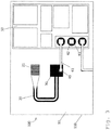
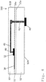
- An electro-optical component 30 is monolithically integrated in one or more semiconductor layers of the chip 110 arranged on the substrate top side 12a of the substrate 12 or on the substrate top side 12a of the substrate 12.
- At least one electrical connection of the monolithically integrated electro-optical component 30 is connected by means of a connecting line 41 to a conductor track connection 43 located below the substrate rear side 12b.
- the connecting line 41 extends through a through hole 42 in the substrate 12 from the electro-optical component 30 to the conductor track connection 43 located below the substrate rear side 12b.
- An electrical component 50 is also monolithically integrated in one or more semiconductor layers of the chip 110 arranged on the substrate top side 12a of the substrate 12 or on the substrate top side 12a of the substrate 12.
- At least one electrical connection of the monolithically integrated electrical component 50 is connected by means of a connecting line 41a to a conductor track connection 43a located below the substrate rear side 12b.
- the connecting line 41a extends through a through hole 42a in the substrate 12 from the electrical component 50 to the conductor track connection 43a located below the substrate rear side 12b.
- the lower side of the chip 110 is placed on a printed circuit board 610, which is a wiring level for the electrical circuit board located on the rear side of the chip or the rear side of the substrate 12b Forms conductor track connections 43 and 43a.
- the circuit board 610 has at least one connecting line 46 which electrically connects the conductor track connection 43a connected to the electrical component 50 and the conductor track connection 43 connected to the electro-optical component 30 to one another.
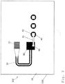
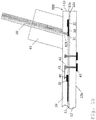
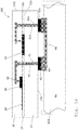
- FIG. 10 shows a further example of an optoelectronic component 100, not according to the invention.
- the component 100 comprises a chip 110 with a substrate 12 and at least one optical waveguide 20 integrated in the chip 110.
- An electro-optical component 30 and an electrical component 50 are monolithically integrated in one or more semiconductor layers of the chip 110 arranged on the substrate top side 12a of the substrate 12 or on the substrate top side 12a of the substrate 12.
- At least one electrical connection of the monolithically integrated electrical component 50 is connected by means of a connecting line 41a to a conductor track connection 43a located below the substrate rear side 12b.
- the connecting line 41a extends through a through hole 42a in the substrate 12 from the electrical component 50 to the conductor track connection 43a located below the substrate rear side 12b.
- the lower side of the chip 110 is placed on a printed circuit board 610 which forms a wiring level for the electrical conductor track connection 43a located on the rear side of the chip or the rear side of the substrate 12b.
- the circuit board 610 has at least one connecting line 46 which connects the conductor track connection 43a connected to the electrical component 50 with another, for reasons of clarity in FIG Figure 15 component not shown connects.
- the electro-optical component 30 and the electrical component 50 are connected by means of at least one line 620 which is arranged on the substrate top side 12 a of the substrate 12.
- the electrical component 50 is in each case directly on the substrate 12 and closes (upward) in each case at the level with the waveguides 20 in the silicon layer 10a.
- the electrical component 50 extends in each case from the substrate 12 into the silicon layer 10a located on the silicon dioxide layer.
Landscapes
- Physics & Mathematics (AREA)
- General Physics & Mathematics (AREA)
- Optics & Photonics (AREA)
- Engineering & Computer Science (AREA)
- Microelectronics & Electronic Packaging (AREA)
- Optical Integrated Circuits (AREA)
- Optical Couplings Of Light Guides (AREA)
Claims (12)
- Composant optoélectronique (100) comprenant une puce (110) comprenant- un substrat (12) et- au moins un guide d'ondes optique (20) intégré dans la puce (110),- un composant électro-optique (30) étant intégré de manière monolithique dans une ou plusieurs couches semi-conductrices de la puce (110), disposées sur la face supérieure (12a) du substrat (12), ou sur la face supérieure (12a) du substrat (12) et- au moins une borne électrique du composant électro-optique (30), intégré de manière monolithique, étant reliée à une première borne de piste conductrice (43), située sous la face arrière (12b) du substrat, au moyen d'une première ligne de liaison (41),- la première ligne de liaison (41) s'étendant à travers un trou traversant (42) ménagé dans le substrat (12) depuis le composant électro-optique (30) à la première borne de piste conductrice (43) située sous la face arrière (12b) du substrat,
caractérisé en ce que- un composant électrique (50) est intégré de manière monolithique dans une ou plusieurs couches semi-conductrices de la puce (110), disposées sur la face supérieure (12a) du substrat (12), ou sur la face supérieure (12a) du substrat (12),- au moins une borne électrique du composant électrique (50), intégré de manière monolithique, est reliée à une deuxième borne de piste conductrice (43a), située sous la face arrière (12b) du substrat, au moyen d'une deuxième ligne de liaison (41a),- la puce (110) est placée avec sa face inférieure sur une carte de circuit imprimé (610) qui forme un plan de câblage des bornes de pistes conductrices électriques (43, 43a) situées sur la face arrière (12b) du substrat, et- la carte de circuit imprimé (610) comporte au moins une troisième ligne de liaison (46) qui relie électriquement la deuxième borne de piste conductrice (43a) et la première borne de piste conductrice (43) l'une à l'autre. - Composant optoélectronique (100) selon la revendication 1,
caractérisé en ce que- au moins une borne optique, de préférence toutes les bornes optiques, sont disposées sur la face supérieure de la puce (110) et- au moins une des bornes électriques, de préférence toutes les bornes électriques, sont disposées sur la face inférieure de la puce (110). - Composant optoélectronique (100) selon l'une des revendications précédentes,
caractérisé en ce que
le composant électro-optique (30), intégré de manière monolithique, est un photodétecteur (32) ou un modulateur (31). - Composant optoélectronique (100) selon l'une des revendications précédentes,
caractérisé en ce que
le guide d'ondes intégré (20) est équipé d'un dispositif de déviation, ou est relié à un tel dispositif qui dévie le rayonnement optique, qui doit être délivré par couplage en sortie du guide d'ondes (20), presque perpendiculairement en direction de la face supérieure de la puce, ou qui dévie le rayonnement, qui est incident à peu près perpendiculairement à la face supérieure de la puce, et l'injecte par couplage dans le guide d'ondes (20). - Composant optoélectronique (100) selon la revendication 4,
caractérisé en ce que
le dispositif de déviation est formé par un coupleur de réseau (21) formé dans le guide d'ondes (20). - Composant optoélectronique (100) selon l'une des revendications précédentes,
caractérisé en ce que- une couche de dioxyde de silicium est placée sur le substrat (12) et une couche de silicium (10a) est placée par-dessus, et- le guide d'ondes optique (20) et le composant électro-optique (30) sont intégrés de manière monolithique dans la couche de silicium (10a). - Composant optoélectronique (100) selon l'une des revendications précédentes,
caractérisé en ce que
le composant électrique (50) intégré de manière monolithique est un amplificateur ou un pilote. - Composant optoélectronique (100) selon l'une des revendications précédentes,
caractérisé en ce que
l'au moins un guide d'ondes intégré (20) ou au moins un des guides d'ondes intégrés (20)- est équipé d'un dispositif de déviation dans la région de l'une de ses extrémités de guide d'ondes, ou est relié à un tel dispositif de déviation, qui injecte par couplage dans le guide d'ondes (20) un rayonnement optique qui provient d'une source de lumière disposée sur la face supérieure de la puce (110) et qui est incident à peu près perpendiculairement à la face supérieure de la puce, et- est équipé d'un dispositif de déviation dans la région de l'autre extrémité du guide d'ondes, ou est relié à un tel dispositif de déviation, qui dévie le rayonnement optique qui doit être délivré par couplage en sortie du guide d'ondes (20) à peu près perpendiculairement en direction de la face supérieure de la puce, notamment en direction d'une fibre optique disposée sur la face supérieure de la puce ou en direction d'un élément de déviation de lumière disposé sur la face supérieure de la puce,- au moins une borne électrique de la source de lumière étant reliée au moyen d'une ligne de liaison à une borne de piste conductrice située sous la face arrière (12b) du substrat. - Composant optoélectronique (100) selon la revendication 8,
caractérisé en ce que
un modulateur est intégré de manière monolithique dans la puce (110) entre les deux extrémités de guide d'ondes et module le rayonnement de la source de lumière avant de l'injecter par couplage dans la fibre optique. - Composant optoélectronique (100) selon l'une des revendications précédentes,
caractérisé en ce que
l'au moins un guide d'ondes intégré (20) ou au moins un des guides d'ondes intégrés (20)- est équipé d'un dispositif de déviation dans la région de l'une de ses extrémités de guide d'ondes, ou est relié à un tel dispositif de déviation, qui injecte par couplage dans le guide d'ondes (20) un rayonnement optique qui provient d'une fibre optique disposée sur la face supérieure de la puce et qui est incident à peu près perpendiculairement à la face supérieure de la puce, et- est relié à un photodétecteur (32), intégré dans la puce (110), dans la région de l'autre extrémité du guide d'ondes. - Composant optoélectronique (100) selon la revendication 10,
caractérisé en ce que
un amplificateur à transimpédance est intégré de manière monolithique dans la puce (110) et amplifie le signal électrique du photodétecteur (32). - Composant optoélectronique (100) selon l'une des revendications précédentes,
caractérisé en ce que- le composant électro-optique (30) et le composant électrique (50) sont reliés au moyen d'une ligne (620) qui est disposée sur la face supérieure (12a) du substrat (12).
Applications Claiming Priority (2)
| Application Number | Priority Date | Filing Date | Title |
|---|---|---|---|
| DE102014219792.9A DE102014219792A1 (de) | 2014-09-30 | 2014-09-30 | Optoelektronisches Bauelement |
| PCT/DE2015/200464 WO2016050243A1 (fr) | 2014-09-30 | 2015-09-28 | Composant optoélectronique |
Publications (2)
| Publication Number | Publication Date |
|---|---|
| EP3201663A1 EP3201663A1 (fr) | 2017-08-09 |
| EP3201663B1 true EP3201663B1 (fr) | 2021-01-06 |
Family
ID=54883942
Family Applications (1)
| Application Number | Title | Priority Date | Filing Date |
|---|---|---|---|
| EP15812943.7A Active EP3201663B1 (fr) | 2014-09-30 | 2015-09-28 | Composant optoélectronique |
Country Status (5)
| Country | Link |
|---|---|
| US (1) | US10775561B2 (fr) |
| EP (1) | EP3201663B1 (fr) |
| CN (1) | CN106716199B (fr) |
| DE (2) | DE102014219792A1 (fr) |
| WO (1) | WO2016050243A1 (fr) |
Families Citing this family (12)
| Publication number | Priority date | Publication date | Assignee | Title |
|---|---|---|---|---|
| US10976491B2 (en) | 2016-11-23 | 2021-04-13 | The Research Foundation For The State University Of New York | Photonics interposer optoelectronics |
| KR20190101362A (ko) * | 2016-11-23 | 2019-08-30 | 더 리서치 파운데이션 포 더 스테이트 유니버시티 오브 뉴욕 | 포토닉스 인터포저 광전자 |
| US10698156B2 (en) * | 2017-04-27 | 2020-06-30 | The Research Foundation For The State University Of New York | Wafer scale bonded active photonics interposer |
| US11315878B2 (en) * | 2018-10-31 | 2022-04-26 | Taiwan Semiconductor Manufacturing Company, Ltd. | Photonics integrated circuit package |
| CN110596830A (zh) * | 2019-09-24 | 2019-12-20 | 武汉光迅科技股份有限公司 | 一种光学组件 |
| US20210096311A1 (en) * | 2019-09-27 | 2021-04-01 | Taiwan Semiconductor Manufacturing Co., Ltd. | Photonic semiconductor device and method of manufacture |
| US11076491B2 (en) | 2019-10-16 | 2021-07-27 | Compass Technology Company Limited | Integrated electro-optical flexible circuit board |
| CN114788018A (zh) * | 2019-12-19 | 2022-07-22 | 电光-Ic股份有限公司 | 包括单片集成的光电二极管和跨阻放大器的光接收器 |
| EP4088327A4 (fr) | 2020-01-08 | 2024-02-07 | Avicenatech Corp | Mise en boîtier pour micro-del pour communication de puce à puce |
| US11609391B2 (en) * | 2020-05-19 | 2023-03-21 | Taiwan Semiconductor Manufacturing Company, Ltd. | Semiconductor package and manufacturing method thereof |
| US11747554B2 (en) * | 2020-05-22 | 2023-09-05 | Ranovus Inc. | Carrier based laser assembly and method of assembly thereof with photonic integrated circuit |
| KR20230037055A (ko) * | 2020-07-20 | 2023-03-15 | 어플라이드 머티어리얼스, 인코포레이티드 | 광학 디바이스들을 위한 통합 전도성 애퍼쳐들 |
Family Cites Families (20)
| Publication number | Priority date | Publication date | Assignee | Title |
|---|---|---|---|---|
| FR2835095B1 (fr) * | 2002-01-22 | 2005-03-18 | Procede de preparation d'ensembles a semi-conducteurs separables, notamment pour former des substrats pour l'electronique, l'optoelectrique et l'optique | |
| FI20031796A (fi) * | 2003-12-09 | 2005-06-10 | Asperation Oy | Menetelmä EMI-suojan rakentamiseksi piirilevylle upotettavan komponentin ympärille |
| US8168939B2 (en) | 2008-07-09 | 2012-05-01 | Luxtera, Inc. | Method and system for a light source assembly supporting direct coupling to an integrated circuit |
| US8831437B2 (en) * | 2009-09-04 | 2014-09-09 | Luxtera, Inc. | Method and system for a photonic interposer |
| US8213751B1 (en) * | 2008-11-26 | 2012-07-03 | Optonet Inc. | Electronic-integration compatible photonic integrated circuit and method for fabricating electronic-integration compatible photonic integrated circuit |
| US9331096B2 (en) * | 2009-09-04 | 2016-05-03 | Luxtera, Inc. | Method and system for hybrid integration of optical communication systems |
| GB0915775D0 (en) | 2009-09-09 | 2009-10-07 | Univ Gent | Implantable sensor |
| US8803269B2 (en) | 2011-05-05 | 2014-08-12 | Cisco Technology, Inc. | Wafer scale packaging platform for transceivers |
| WO2013086047A1 (fr) * | 2011-12-06 | 2013-06-13 | Cornell University | Plateforme d'interconnexion optique à module multipuce intégré |
| US9423560B2 (en) | 2011-12-15 | 2016-08-23 | Alcatel Lucent | Electronic/photonic integrated circuit architecture and method of manufacture thereof |
| US9507086B2 (en) * | 2011-12-30 | 2016-11-29 | Intel Corporation | Optical I/O system using planar light-wave integrated circuit |
| JP6227878B2 (ja) | 2012-03-16 | 2017-11-08 | ラクステラ・インコーポレイテッドLuxtera,Inc. | 光インターポーザのための方法及びシステム |
| EP2839329A4 (fr) * | 2012-04-16 | 2015-12-16 | Hewlett Packard Development Co | Sous-ensemble optique intégré |
| JP2014035546A (ja) * | 2012-08-07 | 2014-02-24 | Luxtera Inc | 光通信システムのハイブリッド集積のための方法及びシステム |
| US9057450B2 (en) * | 2013-03-13 | 2015-06-16 | Elliott Company | Valve exerciser for an emergency shutoff valve of a steam turbine and method for using the same |
| US20140270629A1 (en) * | 2013-03-15 | 2014-09-18 | Apic Corporation | Optical waveguide network of an interconnecting ic module |
| US9091819B2 (en) * | 2013-04-11 | 2015-07-28 | International Business Machines Corporation | Grating edge coupler and method of forming same |
| CN105593747B (zh) * | 2013-06-09 | 2019-07-05 | 光电网股份有限公司 | 超低电压宽调制带宽低光学损耗光学强度或相位调制器 |
| US10606003B2 (en) * | 2013-08-02 | 2020-03-31 | Luxtera, Inc. | Method and system for an optical coupler for silicon photonics devices |
| DE102014219663A1 (de) | 2014-09-29 | 2016-03-31 | Ihp Gmbh - Innovations For High Performance Microelectronics / Leibniz-Institut Für Innovative Mikroelektronik | Photonisch integrierter Chip, optisches Bauelement mit photonisch integriertem Chip und Verfahren zu deren Herstellung |
-
2014
- 2014-09-30 DE DE102014219792.9A patent/DE102014219792A1/de not_active Withdrawn
-
2015
- 2015-09-28 DE DE112015004474.4T patent/DE112015004474A5/de not_active Withdrawn
- 2015-09-28 WO PCT/DE2015/200464 patent/WO2016050243A1/fr active Application Filing
- 2015-09-28 CN CN201580049634.9A patent/CN106716199B/zh active Active
- 2015-09-28 EP EP15812943.7A patent/EP3201663B1/fr active Active
- 2015-09-28 US US15/515,923 patent/US10775561B2/en active Active
Non-Patent Citations (1)
| Title |
|---|
| KNOLL D ET AL: "Monolithically integrated 25Gbit/sec receiver for 1.55[mu]m in photonic BiCMOS technology", OFC 2014, OSA, 9 March 2014 (2014-03-09), pages 1 - 3, XP032632948, DOI: 10.1109/OFC.2014.6886828 * |
Also Published As
| Publication number | Publication date |
|---|---|
| DE102014219792A1 (de) | 2016-03-31 |
| WO2016050243A1 (fr) | 2016-04-07 |
| US10775561B2 (en) | 2020-09-15 |
| CN106716199B (zh) | 2020-02-28 |
| EP3201663A1 (fr) | 2017-08-09 |
| DE112015004474A5 (de) | 2017-06-14 |
| US20190146151A1 (en) | 2019-05-16 |
| CN106716199A (zh) | 2017-05-24 |
Similar Documents
| Publication | Publication Date | Title |
|---|---|---|
| EP3201663B1 (fr) | Composant optoélectronique | |
| DE60208416T2 (de) | Digitale optische netzwerkarchitektur | |
| US10012809B2 (en) | Printed circuit board assembly with a photonic integrated circuit for an electro-optical interface | |
| DE69836058T2 (de) | Mehrkanaliges optisches Empfänger-/Sendersystem | |
| EP0383138A2 (fr) | Dispositif pour la réception optique directe d'une pluralité de longueurs d'ondes | |
| DE102014101671B4 (de) | Bidirektionales optisches Doppel-Wellenlänge-Kommunikationssystem und Verfahren zum Kommunizieren optischer Signale | |
| US7876984B2 (en) | Planar optical waveguide array module and method of fabricating the same | |
| DE10150401A1 (de) | Ausrichten eines optischen Bauelementsystems mit einem optischen Linsensystem | |
| JPWO2006035499A1 (ja) | 光電気集積回路素子およびそれを用いた伝送装置 | |
| DE60219161T2 (de) | Integration optoelektronischer bauelemente | |
| DE112008001441B4 (de) | Optische Verbindung | |
| DE4106721C2 (fr) | ||
| EP2200194B1 (fr) | Module de détecteur | |
| DE102004025659A1 (de) | Optoelektrisches Übertragungsmodul und Verfahren zu dessen Herstellung | |
| DE10213599A1 (de) | Wellenleiterempfänger mit einem Nachverstärker mit einstellbarer Bandbreite | |
| EP0440087B1 (fr) | Dispositif de connexion de signaux optiques pour les tiroirs d'un boîtier à tiroir | |
| DE102019117629A1 (de) | Photonikpackageintegration | |
| JP5800466B2 (ja) | 多チャネル光送信モジュール | |
| EP0442312A2 (fr) | Emetteur et/ou récepteur optique intégré | |
| DE202015106860U1 (de) | Optisches Mehrkanal-Sende- und/oder Empfangsmodul, insbesondere für hochbitratige digitale optische Signale | |
| DE102005062735B4 (de) | Elektrooptische Baugruppe zum Multiplexen bzw. Demultiplexen eines optischen Signals | |
| DE10160508B4 (de) | Anordnung zur Detektion von optischen Signalen mindestens eines optischen Kanals eines planaren optischen Schaltkreises und/oder zur Einkopplung optischer Signale in mindestens einen optischen Kanal eines planaren optischen Schaltkreises | |
| WO2004025341A1 (fr) | Carte de circuits munie de traces conducteurs electriques et de moyens de conversion electro-optique et/ou opto-electrique | |
| DE10319900A1 (de) | Optoelektronische Sende- und/oder Empfangsanordnung | |
| CN107209335B (zh) | 电子/光子芯片集成和接合 |
Legal Events
| Date | Code | Title | Description |
|---|---|---|---|
| STAA | Information on the status of an ep patent application or granted ep patent |
Free format text: STATUS: THE INTERNATIONAL PUBLICATION HAS BEEN MADE |
|
| PUAI | Public reference made under article 153(3) epc to a published international application that has entered the european phase |
Free format text: ORIGINAL CODE: 0009012 |
|
| STAA | Information on the status of an ep patent application or granted ep patent |
Free format text: STATUS: REQUEST FOR EXAMINATION WAS MADE |
|
| 17P | Request for examination filed |
Effective date: 20170428 |
|
| AK | Designated contracting states |
Kind code of ref document: A1 Designated state(s): AL AT BE BG CH CY CZ DE DK EE ES FI FR GB GR HR HU IE IS IT LI LT LU LV MC MK MT NL NO PL PT RO RS SE SI SK SM TR |
|
| AX | Request for extension of the european patent |
Extension state: BA ME |
|
| DAV | Request for validation of the european patent (deleted) | ||
| DAX | Request for extension of the european patent (deleted) | ||
| STAA | Information on the status of an ep patent application or granted ep patent |
Free format text: STATUS: EXAMINATION IS IN PROGRESS |
|
| 17Q | First examination report despatched |
Effective date: 20190104 |
|
| GRAP | Despatch of communication of intention to grant a patent |
Free format text: ORIGINAL CODE: EPIDOSNIGR1 |
|
| STAA | Information on the status of an ep patent application or granted ep patent |
Free format text: STATUS: GRANT OF PATENT IS INTENDED |
|
| INTG | Intention to grant announced |
Effective date: 20200806 |
|
| GRAS | Grant fee paid |
Free format text: ORIGINAL CODE: EPIDOSNIGR3 |
|
| GRAA | (expected) grant |
Free format text: ORIGINAL CODE: 0009210 |
|
| STAA | Information on the status of an ep patent application or granted ep patent |
Free format text: STATUS: THE PATENT HAS BEEN GRANTED |
|
| AK | Designated contracting states |
Kind code of ref document: B1 Designated state(s): AL AT BE BG CH CY CZ DE DK EE ES FI FR GB GR HR HU IE IS IT LI LT LU LV MC MK MT NL NO PL PT RO RS SE SI SK SM TR |
|
| REG | Reference to a national code |
Ref country code: GB Ref legal event code: FG4D |
|
| REG | Reference to a national code |
Ref country code: AT Ref legal event code: REF Ref document number: 1352989 Country of ref document: AT Kind code of ref document: T Effective date: 20210115 Ref country code: CH Ref legal event code: EP |
|
| REG | Reference to a national code |
Ref country code: DE Ref legal event code: R096 Ref document number: 502015014133 Country of ref document: DE |
|
| REG | Reference to a national code |
Ref country code: IE Ref legal event code: FG4D Free format text: LANGUAGE OF EP DOCUMENT: GERMAN |
|
| REG | Reference to a national code |
Ref country code: NL Ref legal event code: FP |
|
| RAP2 | Party data changed (patent owner data changed or rights of a patent transferred) |
Owner name: SICOYA GMBH |
|
| REG | Reference to a national code |
Ref country code: LT Ref legal event code: MG9D |
|
| PG25 | Lapsed in a contracting state [announced via postgrant information from national office to epo] |
Ref country code: LT Free format text: LAPSE BECAUSE OF FAILURE TO SUBMIT A TRANSLATION OF THE DESCRIPTION OR TO PAY THE FEE WITHIN THE PRESCRIBED TIME-LIMIT Effective date: 20210106 Ref country code: PT Free format text: LAPSE BECAUSE OF FAILURE TO SUBMIT A TRANSLATION OF THE DESCRIPTION OR TO PAY THE FEE WITHIN THE PRESCRIBED TIME-LIMIT Effective date: 20210506 Ref country code: NO Free format text: LAPSE BECAUSE OF FAILURE TO SUBMIT A TRANSLATION OF THE DESCRIPTION OR TO PAY THE FEE WITHIN THE PRESCRIBED TIME-LIMIT Effective date: 20210406 Ref country code: HR Free format text: LAPSE BECAUSE OF FAILURE TO SUBMIT A TRANSLATION OF THE DESCRIPTION OR TO PAY THE FEE WITHIN THE PRESCRIBED TIME-LIMIT Effective date: 20210106 Ref country code: GR Free format text: LAPSE BECAUSE OF FAILURE TO SUBMIT A TRANSLATION OF THE DESCRIPTION OR TO PAY THE FEE WITHIN THE PRESCRIBED TIME-LIMIT Effective date: 20210407 Ref country code: FI Free format text: LAPSE BECAUSE OF FAILURE TO SUBMIT A TRANSLATION OF THE DESCRIPTION OR TO PAY THE FEE WITHIN THE PRESCRIBED TIME-LIMIT Effective date: 20210106 Ref country code: BG Free format text: LAPSE BECAUSE OF FAILURE TO SUBMIT A TRANSLATION OF THE DESCRIPTION OR TO PAY THE FEE WITHIN THE PRESCRIBED TIME-LIMIT Effective date: 20210406 |
|
| REG | Reference to a national code |
Ref country code: DE Ref legal event code: R081 Ref document number: 502015014133 Country of ref document: DE Owner name: SICOYA GMBH, DE Free format text: FORMER OWNER: TECHNISCHE UNIVERSITAET BERLIN, 10623 BERLIN, DE |
|
| PG25 | Lapsed in a contracting state [announced via postgrant information from national office to epo] |
Ref country code: SE Free format text: LAPSE BECAUSE OF FAILURE TO SUBMIT A TRANSLATION OF THE DESCRIPTION OR TO PAY THE FEE WITHIN THE PRESCRIBED TIME-LIMIT Effective date: 20210106 Ref country code: PL Free format text: LAPSE BECAUSE OF FAILURE TO SUBMIT A TRANSLATION OF THE DESCRIPTION OR TO PAY THE FEE WITHIN THE PRESCRIBED TIME-LIMIT Effective date: 20210106 Ref country code: LV Free format text: LAPSE BECAUSE OF FAILURE TO SUBMIT A TRANSLATION OF THE DESCRIPTION OR TO PAY THE FEE WITHIN THE PRESCRIBED TIME-LIMIT Effective date: 20210106 Ref country code: RS Free format text: LAPSE BECAUSE OF FAILURE TO SUBMIT A TRANSLATION OF THE DESCRIPTION OR TO PAY THE FEE WITHIN THE PRESCRIBED TIME-LIMIT Effective date: 20210106 |
|
| PG25 | Lapsed in a contracting state [announced via postgrant information from national office to epo] |
Ref country code: IS Free format text: LAPSE BECAUSE OF FAILURE TO SUBMIT A TRANSLATION OF THE DESCRIPTION OR TO PAY THE FEE WITHIN THE PRESCRIBED TIME-LIMIT Effective date: 20210506 |
|
| REG | Reference to a national code |
Ref country code: DE Ref legal event code: R097 Ref document number: 502015014133 Country of ref document: DE |
|
| REG | Reference to a national code |
Ref country code: GB Ref legal event code: 732E Free format text: REGISTERED BETWEEN 20210923 AND 20210929 |
|
| PG25 | Lapsed in a contracting state [announced via postgrant information from national office to epo] |
Ref country code: CZ Free format text: LAPSE BECAUSE OF FAILURE TO SUBMIT A TRANSLATION OF THE DESCRIPTION OR TO PAY THE FEE WITHIN THE PRESCRIBED TIME-LIMIT Effective date: 20210106 Ref country code: EE Free format text: LAPSE BECAUSE OF FAILURE TO SUBMIT A TRANSLATION OF THE DESCRIPTION OR TO PAY THE FEE WITHIN THE PRESCRIBED TIME-LIMIT Effective date: 20210106 Ref country code: SM Free format text: LAPSE BECAUSE OF FAILURE TO SUBMIT A TRANSLATION OF THE DESCRIPTION OR TO PAY THE FEE WITHIN THE PRESCRIBED TIME-LIMIT Effective date: 20210106 |
|
| PLBE | No opposition filed within time limit |
Free format text: ORIGINAL CODE: 0009261 |
|
| STAA | Information on the status of an ep patent application or granted ep patent |
Free format text: STATUS: NO OPPOSITION FILED WITHIN TIME LIMIT |
|
| PG25 | Lapsed in a contracting state [announced via postgrant information from national office to epo] |
Ref country code: SK Free format text: LAPSE BECAUSE OF FAILURE TO SUBMIT A TRANSLATION OF THE DESCRIPTION OR TO PAY THE FEE WITHIN THE PRESCRIBED TIME-LIMIT Effective date: 20210106 Ref country code: DK Free format text: LAPSE BECAUSE OF FAILURE TO SUBMIT A TRANSLATION OF THE DESCRIPTION OR TO PAY THE FEE WITHIN THE PRESCRIBED TIME-LIMIT Effective date: 20210106 Ref country code: RO Free format text: LAPSE BECAUSE OF FAILURE TO SUBMIT A TRANSLATION OF THE DESCRIPTION OR TO PAY THE FEE WITHIN THE PRESCRIBED TIME-LIMIT Effective date: 20210106 |
|
| 26N | No opposition filed |
Effective date: 20211007 |
|
| REG | Reference to a national code |
Ref country code: NL Ref legal event code: PD Owner name: SICOYA GMBH; DE Free format text: DETAILS ASSIGNMENT: CHANGE OF OWNER(S), ASSIGNMENT; FORMER OWNER NAME: TECHNISCHE UNIVERSITAET BERLIN Effective date: 20211123 |
|
| REG | Reference to a national code |
Ref country code: BE Ref legal event code: PD Owner name: SICOYA GMBH; DE Free format text: DETAILS ASSIGNMENT: CHANGE OF OWNER(S), ASSIGNMENT; FORMER OWNER NAME: TECHNISCHE UNIVERSITAET BERLIN Effective date: 20211104 |
|
| PG25 | Lapsed in a contracting state [announced via postgrant information from national office to epo] |
Ref country code: AL Free format text: LAPSE BECAUSE OF FAILURE TO SUBMIT A TRANSLATION OF THE DESCRIPTION OR TO PAY THE FEE WITHIN THE PRESCRIBED TIME-LIMIT Effective date: 20210106 Ref country code: ES Free format text: LAPSE BECAUSE OF FAILURE TO SUBMIT A TRANSLATION OF THE DESCRIPTION OR TO PAY THE FEE WITHIN THE PRESCRIBED TIME-LIMIT Effective date: 20210106 |
|
| PG25 | Lapsed in a contracting state [announced via postgrant information from national office to epo] |
Ref country code: SI Free format text: LAPSE BECAUSE OF FAILURE TO SUBMIT A TRANSLATION OF THE DESCRIPTION OR TO PAY THE FEE WITHIN THE PRESCRIBED TIME-LIMIT Effective date: 20210106 |
|
| PG25 | Lapsed in a contracting state [announced via postgrant information from national office to epo] |
Ref country code: IT Free format text: LAPSE BECAUSE OF FAILURE TO SUBMIT A TRANSLATION OF THE DESCRIPTION OR TO PAY THE FEE WITHIN THE PRESCRIBED TIME-LIMIT Effective date: 20210106 |
|
| REG | Reference to a national code |
Ref country code: CH Ref legal event code: PL |
|
| PG25 | Lapsed in a contracting state [announced via postgrant information from national office to epo] |
Ref country code: IS Free format text: LAPSE BECAUSE OF FAILURE TO SUBMIT A TRANSLATION OF THE DESCRIPTION OR TO PAY THE FEE WITHIN THE PRESCRIBED TIME-LIMIT Effective date: 20210506 Ref country code: MC Free format text: LAPSE BECAUSE OF FAILURE TO SUBMIT A TRANSLATION OF THE DESCRIPTION OR TO PAY THE FEE WITHIN THE PRESCRIBED TIME-LIMIT Effective date: 20210106 |
|
| PG25 | Lapsed in a contracting state [announced via postgrant information from national office to epo] |
Ref country code: LU Free format text: LAPSE BECAUSE OF NON-PAYMENT OF DUE FEES Effective date: 20210928 Ref country code: IE Free format text: LAPSE BECAUSE OF NON-PAYMENT OF DUE FEES Effective date: 20210928 |
|
| PG25 | Lapsed in a contracting state [announced via postgrant information from national office to epo] |
Ref country code: LI Free format text: LAPSE BECAUSE OF NON-PAYMENT OF DUE FEES Effective date: 20210930 Ref country code: CH Free format text: LAPSE BECAUSE OF NON-PAYMENT OF DUE FEES Effective date: 20210930 |
|
| REG | Reference to a national code |
Ref country code: AT Ref legal event code: MM01 Ref document number: 1352989 Country of ref document: AT Kind code of ref document: T Effective date: 20210928 |
|
| PG25 | Lapsed in a contracting state [announced via postgrant information from national office to epo] |
Ref country code: AT Free format text: LAPSE BECAUSE OF NON-PAYMENT OF DUE FEES Effective date: 20210928 |
|
| PG25 | Lapsed in a contracting state [announced via postgrant information from national office to epo] |
Ref country code: HU Free format text: LAPSE BECAUSE OF FAILURE TO SUBMIT A TRANSLATION OF THE DESCRIPTION OR TO PAY THE FEE WITHIN THE PRESCRIBED TIME-LIMIT; INVALID AB INITIO Effective date: 20150928 |
|
| PG25 | Lapsed in a contracting state [announced via postgrant information from national office to epo] |
Ref country code: CY Free format text: LAPSE BECAUSE OF FAILURE TO SUBMIT A TRANSLATION OF THE DESCRIPTION OR TO PAY THE FEE WITHIN THE PRESCRIBED TIME-LIMIT Effective date: 20210106 |
|
| PGFP | Annual fee paid to national office [announced via postgrant information from national office to epo] |
Ref country code: NL Payment date: 20230920 Year of fee payment: 9 Ref country code: GB Payment date: 20230921 Year of fee payment: 9 |
|
| PGFP | Annual fee paid to national office [announced via postgrant information from national office to epo] |
Ref country code: FR Payment date: 20230919 Year of fee payment: 9 Ref country code: DE Payment date: 20230930 Year of fee payment: 9 Ref country code: BE Payment date: 20230918 Year of fee payment: 9 |
|
| PG25 | Lapsed in a contracting state [announced via postgrant information from national office to epo] |
Ref country code: MK Free format text: LAPSE BECAUSE OF FAILURE TO SUBMIT A TRANSLATION OF THE DESCRIPTION OR TO PAY THE FEE WITHIN THE PRESCRIBED TIME-LIMIT Effective date: 20210106 |