EP3200571A1 - Electronic component mounting board and light emission device using same - Google Patents
Electronic component mounting board and light emission device using same Download PDFInfo
- Publication number
- EP3200571A1 EP3200571A1 EP15844693.0A EP15844693A EP3200571A1 EP 3200571 A1 EP3200571 A1 EP 3200571A1 EP 15844693 A EP15844693 A EP 15844693A EP 3200571 A1 EP3200571 A1 EP 3200571A1
- Authority
- EP
- European Patent Office
- Prior art keywords
- layer
- electronic component
- component mounting
- crevices
- ceramic layer
- Prior art date
- Legal status (The legal status is an assumption and is not a legal conclusion. Google has not performed a legal analysis and makes no representation as to the accuracy of the status listed.)
- Granted
Links
Images




Classifications
-
- H—ELECTRICITY
- H05—ELECTRIC TECHNIQUES NOT OTHERWISE PROVIDED FOR
- H05K—PRINTED CIRCUITS; CASINGS OR CONSTRUCTIONAL DETAILS OF ELECTRIC APPARATUS; MANUFACTURE OF ASSEMBLAGES OF ELECTRICAL COMPONENTS
- H05K1/00—Printed circuits
- H05K1/02—Details
- H05K1/03—Use of materials for the substrate
- H05K1/05—Insulated conductive substrates, e.g. insulated metal substrate
- H05K1/053—Insulated conductive substrates, e.g. insulated metal substrate the metal substrate being covered by an inorganic insulating layer
-
- H—ELECTRICITY
- H10—SEMICONDUCTOR DEVICES; ELECTRIC SOLID-STATE DEVICES NOT OTHERWISE PROVIDED FOR
- H10H—INORGANIC LIGHT-EMITTING SEMICONDUCTOR DEVICES HAVING POTENTIAL BARRIERS
- H10H20/00—Individual inorganic light-emitting semiconductor devices having potential barriers, e.g. light-emitting diodes [LED]
- H10H20/80—Constructional details
- H10H20/85—Packages
- H10H20/8506—Containers
-
- H—ELECTRICITY
- H05—ELECTRIC TECHNIQUES NOT OTHERWISE PROVIDED FOR
- H05K—PRINTED CIRCUITS; CASINGS OR CONSTRUCTIONAL DETAILS OF ELECTRIC APPARATUS; MANUFACTURE OF ASSEMBLAGES OF ELECTRICAL COMPONENTS
- H05K1/00—Printed circuits
- H05K1/02—Details
- H05K1/03—Use of materials for the substrate
- H05K1/05—Insulated conductive substrates, e.g. insulated metal substrate
-
- H—ELECTRICITY
- H10—SEMICONDUCTOR DEVICES; ELECTRIC SOLID-STATE DEVICES NOT OTHERWISE PROVIDED FOR
- H10H—INORGANIC LIGHT-EMITTING SEMICONDUCTOR DEVICES HAVING POTENTIAL BARRIERS
- H10H20/00—Individual inorganic light-emitting semiconductor devices having potential barriers, e.g. light-emitting diodes [LED]
- H10H20/80—Constructional details
- H10H20/85—Packages
-
- H—ELECTRICITY
- H10—SEMICONDUCTOR DEVICES; ELECTRIC SOLID-STATE DEVICES NOT OTHERWISE PROVIDED FOR
- H10H—INORGANIC LIGHT-EMITTING SEMICONDUCTOR DEVICES HAVING POTENTIAL BARRIERS
- H10H20/00—Individual inorganic light-emitting semiconductor devices having potential barriers, e.g. light-emitting diodes [LED]
- H10H20/80—Constructional details
- H10H20/85—Packages
- H10H20/857—Interconnections, e.g. lead-frames, bond wires or solder balls
-
- H—ELECTRICITY
- H10—SEMICONDUCTOR DEVICES; ELECTRIC SOLID-STATE DEVICES NOT OTHERWISE PROVIDED FOR
- H10H—INORGANIC LIGHT-EMITTING SEMICONDUCTOR DEVICES HAVING POTENTIAL BARRIERS
- H10H20/00—Individual inorganic light-emitting semiconductor devices having potential barriers, e.g. light-emitting diodes [LED]
- H10H20/80—Constructional details
- H10H20/85—Packages
- H10H20/858—Means for heat extraction or cooling
- H10H20/8581—Means for heat extraction or cooling characterised by their material
-
- H—ELECTRICITY
- H10—SEMICONDUCTOR DEVICES; ELECTRIC SOLID-STATE DEVICES NOT OTHERWISE PROVIDED FOR
- H10H—INORGANIC LIGHT-EMITTING SEMICONDUCTOR DEVICES HAVING POTENTIAL BARRIERS
- H10H20/00—Individual inorganic light-emitting semiconductor devices having potential barriers, e.g. light-emitting diodes [LED]
- H10H20/80—Constructional details
- H10H20/85—Packages
- H10H20/858—Means for heat extraction or cooling
- H10H20/8585—Means for heat extraction or cooling being an interconnection
-
- F—MECHANICAL ENGINEERING; LIGHTING; HEATING; WEAPONS; BLASTING
- F21—LIGHTING
- F21S—NON-PORTABLE LIGHTING DEVICES; SYSTEMS THEREOF; VEHICLE LIGHTING DEVICES SPECIALLY ADAPTED FOR VEHICLE EXTERIORS
- F21S41/00—Illuminating devices specially adapted for vehicle exteriors, e.g. headlamps
- F21S41/10—Illuminating devices specially adapted for vehicle exteriors, e.g. headlamps characterised by the light source
- F21S41/14—Illuminating devices specially adapted for vehicle exteriors, e.g. headlamps characterised by the light source characterised by the type of light source
- F21S41/141—Light emitting diodes [LED]
-
- F—MECHANICAL ENGINEERING; LIGHTING; HEATING; WEAPONS; BLASTING
- F21—LIGHTING
- F21S—NON-PORTABLE LIGHTING DEVICES; SYSTEMS THEREOF; VEHICLE LIGHTING DEVICES SPECIALLY ADAPTED FOR VEHICLE EXTERIORS
- F21S41/00—Illuminating devices specially adapted for vehicle exteriors, e.g. headlamps
- F21S41/10—Illuminating devices specially adapted for vehicle exteriors, e.g. headlamps characterised by the light source
- F21S41/19—Attachment of light sources or lamp holders
- F21S41/192—Details of lamp holders, terminals or connectors
-
- F—MECHANICAL ENGINEERING; LIGHTING; HEATING; WEAPONS; BLASTING
- F21—LIGHTING
- F21S—NON-PORTABLE LIGHTING DEVICES; SYSTEMS THEREOF; VEHICLE LIGHTING DEVICES SPECIALLY ADAPTED FOR VEHICLE EXTERIORS
- F21S45/00—Arrangements within vehicle lighting devices specially adapted for vehicle exteriors, for purposes other than emission or distribution of light
- F21S45/40—Cooling of lighting devices
- F21S45/47—Passive cooling, e.g. using fins, thermal conductive elements or openings
-
- H—ELECTRICITY
- H05—ELECTRIC TECHNIQUES NOT OTHERWISE PROVIDED FOR
- H05K—PRINTED CIRCUITS; CASINGS OR CONSTRUCTIONAL DETAILS OF ELECTRIC APPARATUS; MANUFACTURE OF ASSEMBLAGES OF ELECTRICAL COMPONENTS
- H05K3/00—Apparatus or processes for manufacturing printed circuits
- H05K3/38—Improvement of the adhesion between the insulating substrate and the metal
- H05K3/381—Improvement of the adhesion between the insulating substrate and the metal by special treatment of the substrate
-
- H—ELECTRICITY
- H10—SEMICONDUCTOR DEVICES; ELECTRIC SOLID-STATE DEVICES NOT OTHERWISE PROVIDED FOR
- H10H—INORGANIC LIGHT-EMITTING SEMICONDUCTOR DEVICES HAVING POTENTIAL BARRIERS
- H10H20/00—Individual inorganic light-emitting semiconductor devices having potential barriers, e.g. light-emitting diodes [LED]
- H10H20/80—Constructional details
- H10H20/85—Packages
- H10H20/858—Means for heat extraction or cooling
- H10H20/8582—Means for heat extraction or cooling characterised by their shape
Definitions
- the present invention relates to an electronic component mounting substrate for mounting of a high heat generating component such for example as a light emitting element, and a light emission device using the electronic component mounting substrate, and more particularly relates to an electronic component mounting substrate suitably used for a vehicle-installed LED (Light Emitting Diode) lamp, and a light emission device incorporating the electronic component mounting substrate.
- a high heat generating component such for example as a light emitting element
- a light emission device using the electronic component mounting substrate
- an electronic component mounting substrate suitably used for a vehicle-installed LED (Light Emitting Diode) lamp, and a light emission device incorporating the electronic component mounting substrate.
- LED Light Emitting Diode
- LED lamps have come to be used for car headlights.
- a high-power LED chip is used for a vehicle-installed LED lamp, wherefore a substrate for the mounting of the LED chip is required to have high heat-dissipation capability.
- a substrate for the mounting of the LED chip is required to have high heat-dissipation capability.
- it has been customary to use an aluminum nitride substrate having high thermal conductivity for a vehicle-installed LED lamp.
- a substrate which has high thermal conductivity and yet is inexpensive to manufacture is disclosed in Japanese Unexamined Patent Publication JP-A 2007-165751 .
- the substrate disclosed in JP-A 2007-165751 is constructed by forming an alumite layer on the surface of an aluminum substrate, forming cracks in the alumite layer by, for example, application of thermal stress, and forming a thermally-conductive resin insulating layer on the surface of the crack-bearing alumite layer.
- the thermally-conductive resin insulating layer is formed of resin and thus exhibits hygroscopicity, wherefore ion migration may occur. Furthermore, due to a large difference in thermal expansion coefficient between resin and alumite, the alumite layer and the thermally-conductive resin insulating layer may be separated from each other under thermal history, which results in deterioration in thermal conductivity.
- the invention has been devised in view of the problems as discussed supra, and accordingly an object thereof is to provide an electronic component mounting substrate which excels in resistance to migration, and is thus capable of maintaining high thermal conductivity and insulation performance for a long period of time, and also provide a light emission device using the electronic component mounting substrate.
- An electronic component mounting substrate comprises: a metallic substrate formed of aluminum or an aluminum-based alloy; an alumite layer disposed on the metallic substrate, having a network of crevices at an upper surface thereof; and a ceramic layer disposed on the alumite layer, part of the ceramic layer extending into the crevices.
- a light emission device comprises: the electronic component mounting substrate mentioned above; and a light emitting element mounted on the electronic component mounting substrate.
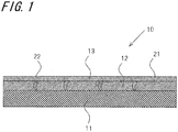
- FIG. 1 is a sectional view showing the structure of an electronic component mounting substrate 10 in accordance with an embodiment of the invention.
- the electronic component mounting substrate 10 is configured for dissipation of heat to the outside, and more specifically, is used for mounting of a LED lamp.
- One particular application of the electronic component mounting substrate 10 is to mounting of a vehicle-installed LED lamp.
- the LED lamp When applied to a vehicle-installed headlight, the LED lamp needs to be designed to emit light in a larger amount, and, in addition to the increase of the amount of light emission, as contrasted to a LED lamp mounted in a common portable terminal or the like, the LED lamp generates a larger amount of heat.
- the electronic component mounting substrate 10 in accordance with an embodiment of the invention is used.
- the electronic component mounting substrate 10 comprises: a metallic substrate 11 formed of aluminum or an aluminum-based alloy; an alumite layer 12, formed on the metallic substrate 11, having a network of crevices 22 at an upper surface 21 thereof; and a ceramic layer 13 which covers the alumite layer 12 formed on the alumite layer 12, part of which extends into the crevices 22.
- FIG. 2 is a sectional view showing an example of procedures in the manufacture of the electronic component mounting substrate 10 in accordance with the present embodiment of the invention.
- FIG. 2(a) shows the metallic substrate 11.
- the metallic substrate 11 is a plate-like body formed of a metal material such as aluminum or an aluminum-based alloy.
- Preferred examples of the aluminum-based alloy include an Al-Cu alloy, an Al-Mn alloy, an Al-Si alloy, an Al-Mg alloy, an Al-Mg-Si alloy, and an Al-Zn-Mg alloy.
- a metal plate body having a thickness of 0.3 [mm] or more and 5 [mm] or less is suitably used as the metallic substrate 11.
- the metallic substrate 1 having a thickness of 0.3 [mm] or more is capable of effectively absorbing heat emanating from a LED lamp and readily dissipating the heat to the outside. Moreover, the metallic substrate 1 having a thickness of 5 [mm] or less affords the advantage of allowing a wiring board to be made lower in profile while providing similar effects to those produced by a heat-radiating plate.
- FIG. 2(b) shows the metallic substrate 11 depicted in FIG. 2(a) , with the alumite layer 12 formed on one side in the thickness direction thereof.
- the alumite layer 12 is formed by anodizing the above-described one side of the metallic substrate 11 in a treatment bath of electrolyte such as sulfuric acid or oxalic acid.
- the thickness of the alumite layer 12 can be adjusted by making adjustment to electrolysis conditions to be fulfilled in the anodization process. For example, the thickness is adjusted to fall in a range of 3 [ ⁇ m] or more and 20 [ ⁇ m] or less.
- the thickness of the alumite layer 12 corresponds to the thickness of other part of the alumite layer 12 than the part formed with the crevices 22 that will hereafter be described.
- the alumite layer 12 having a thickness of 3 [ ⁇ m] or more affords the advantage of raising the level of insulation relative to the metallic substrate 11.
- the alumite layer 12 having a thickness of 20 [ ⁇ m] or less affords the advantage of enhancing the thermal conductivity of the electronic component mounting substrate 10.
- FIG. 2(c) shows the alumite layer 12 depicted in FIG. 2(b) , with the crevices 22 formed at the upper surface 21, or equivalently a surface of the alumite layer 12 opposite to the metallic substrate 11-side surface.
- the crevices 22 are formed so as to open into the upper surface 21 of the alumite layer 12.
- a network of the crevices 22 is formed intentionally.
- the crevices 22 may be formed by subjecting a plurality of minute holes formed at the surface of the alumite layer 12 to mechanical shock, or may be formed through application of thermal stress (thermal shock) entailed by a temperature change which is greater in extent than the temperature change expected during the use of the electronic component mounting substrate.
- a network of the crevices 22 refers to voids or cracks, and is also construed as encompassing a plurality of branched portions of a single crevice.
- FIG. 2(d) shows the alumite layer 12 depicted in FIG. 2(c) , with the ceramic layer 13 formed thereon.
- the ceramic layer 13 is formed by a technique such for example as the sol-gel method.
- a slurry is prepared as a key ingredient of the ceramic layer 13, and, the slurry is coated on the upper surface 21 of the alumite layer 12 by a coating technique such as the dip coating method or the spray coating method.
- the coating and the metallic substrate 11 are heated altogether at temperatures ranging from, for example, 100 [°C] or above to 300 [°C] or below, whereupon the coating is cured.
- the ceramic layer 13 which covers the upper surface 21 of the alumite layer 12 is formed, with part thereof extending into the crevices 22. From the standpoint of ensuring higher level of insulation for the surface of the metallic substrate 11, as shown in FIG. 1 , the ceramic layer 13 fully fills the crevices 22 so as to cover the surface of the metallic substrate 11 exposed at the crevices 22.
- the ceramic layer 13 structurally reinforces the alumite layer 12. This makes it possible to inhibit further formation of cracks in the alumite layer 12 caused by, for example, temperature changes, and thereby maintain the insulation for the surface of the metallic substrate 11 for a long period of time. It is preferable that part of the ceramic layer 13 fills the crevices 22 formed so as to reach the interface between the metallic substrate 11 and the alumite layer 12. In the case where the ceramic layer 13 extends into the crevices 22, air in the crevices 22 is reduced, thus minimizing deterioration in insulation at the surface of the metallic substrate 11 caused by moisture content in the air. Moreover, the strength of adhesion between the ceramic layer 13 and the alumite layer 12 is increased, wherefore the ceramic layer 13 becomes resistant to separation even when undergoing thermal contraction or thermal expansion.
- the ceramic layer 13 is formed of a mixture of alumina and silica. This makes it possible to lower the heating temperature in the process of forming the ceramic layer 13, and thereby produce the electronic component mounting substrate 10 characterized by small thermal stress and high reliability. Moreover, with the alumina content, the ceramic layer 13 lying within the crevices 22 is similar in crystalline structure to the alumite layer 12. This makes it possible to produce the electronic component mounting substrate 10 having higher thermal conductivity.
- the alumina-silica mixture can be prepared by blending alkoxysilane with a slurry formed of alumina powder, silica powder, alcohol, and water. The mixture is subjected to hydrolysis and polycondensation reaction to form the ceramic layer 13 formed of alumina and silica.
- the mixing ratio of alumina to silica is set at 10:90.
- zirconia powder may be added for adjustment of coefficients of thermal expansion.
- the thickness of the ceramic layer 13 is adjusted to fall in a range of 0.5 [ ⁇ m] or more and 10 [ ⁇ m] or less.
- the ceramic layer 13 having a thickness of 0.5 [ ⁇ m] or more is capable of filling the plurality of crevices 22 formed in the alumite layer 12.
- the ceramic layer 13 having a thickness of 20 [ ⁇ m] or less affords the advantage of enhancing the thermal conductivity of the electronic component mounting substrate 10.
- the ceramic layer 13 is provided with a recess 13b located so as to overlap with the crevices 22.
- a wiring conductor 14 can be disposed on the principal surface of the ceramic layer 13 while lying within the recess 13b.
- the width and depth of the recess 13b can be changed by suitably adjusting, for example, the viscosity of the alumina-silica mixture which constitutes the ceramic layer 13.
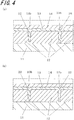
- the recess 13b may be made larger in width than the crevices 22 as shown in FIG. 4(a) , by making the recess 13b smaller in width than the crevices 22 as shown in FIG. 4(b) , it is possible to effectively reduce a decrease in the thickness of a part of the ceramic layer 13 which bears the recess 13b, and thereby render the part of the ceramic layer 13 which corresponds to the recess 13b more resistant to cracking or the like, thus preventing separation of the ceramic layer 13.
- the wiring conductor 14 is disposed on the ceramic layer 13, and a light emitting element 2 such as a light emitting device is mounted thereon.
- the wiring conductor 14 comprises a tightly-adherent metallic layer and a barrier layer.
- the tightly-adherent metallic layer constituting the wiring conductor 14 is disposed on the ceramic layer 13.
- the tightly-adherent metallic layer is formed of, for example, tantalum nitride, a nickel-chromium material, a nickel-chromium-silicon material, a tungsten-silicon material, a molybdenum-silicon material, tungsten, molybdenum, titanium, or chromium.
- the tightly-adherent metallic layer is deposited on the ceramic layer 13 by a thin-film forming technique such as vapor deposition, ion plating, or sputtering.
- the metallic substrate 11 formed with the alumite layer 12 and the ceramic layer 13 is set in a film-forming chamber of a vacuum evaporator, and, a metal piece for constituting the tightly-adherent metallic layer is placed at an evaporation source in the film-forming chamber.
- the interior of the film-forming chamber is vacuumed (under pressure of 10 -2 Pa or below), and, the metal piece placed at the evaporation source is evaporated under heat.
- the molecules of the evaporated metal piece are deposited onto the metallic substrate 11 provided with the alumite layer 12 and the ceramic layer 13, whereupon the tightly-adherent metallic layer is formed.
- the barrier layer which exhibits good adherability and wettability relative to the tightly-adherent metallic layer and a plating layer, and serves to join the tightly-adherent metallic layer with the plating layer firmly, as well as to suppress mutual diffusion of the tightly-adherent metallic layer and the plating layer.
- the barrier layer is formed of, for example, a nickel-chromium material, platinum, palladium, nickel, or cobalt. The barrier layer is deposited on the surface of the tightly-adherent metallic layer by a thin-film forming technique such as vapor deposition, ion plating, or sputtering.
- the thickness of the tightly-adherent metallic layer falls in a range of about 0.01 to 0.5 [ ⁇ m]. If the thickness of the tightly-adherent metallic layer is less than 0.01 [ ⁇ m], it is prone to be difficult to cause the tightly-adherent metallic layer to adhere to the ceramic layer 13 firmly. On the other hand, if the thickness of the tightly-adherent metallic layer exceeds 0.5 [ ⁇ m], the tightly-adherent metallic layer will be prone to separation under internal stress applied during the tightly-adherent metallic layer-forming process. Moreover, it is advisable that the thickness of the barrier layer falls in a range of about 0.05 to 1 [ ⁇ m].
- the barrier layer may suffer defects such as pinholes and is less prone to serve the intended purposes.
- the thickness of the barrier layer exceeds 1 [ ⁇ m] the barrier layer will be prone to separation under internal stress applied during the barrier layer-forming process.
- a metal layer composed of copper, gold or the like may be put on the barrier layer to achieve satisfactory metallic-layer formation on the wiring conductor 14.
- a metal layer is formed in a manner similar to the wiring conductor 14-forming process.
- the metallic layer is formed by laminating a plating layer formed of copper or silver on the wiring conductor 14 disposed on the metallic substrate 11 via the alumite layer 12 and the ceramic layer 13.
- the metallic layer conducts heat to a greater extent when formed of a material which is higher in thermal conductivity than the material of construction of the wiring conductor 14.
- a metallic plating layer is deposited on the exposed surface of the wiring conductor 14 by electroplating or electroless plating.
- the metallic plating layer is formed of a metal which excels in corrosion resistance and in connection with a connecting member 3, such as nickel, gold, or silver.
- a nickel plating layer having a thickness of about 0.5 to 5 [ ⁇ m] and a gold plating layer having a thickness of about 0.1 to 3 [ ⁇ m] or a nickel plating layer having a thickness of about 1 to 10 [ ⁇ m] and a silver plating layer having a thickness of about 0.1 to 1 [ ⁇ m] are successively deposited.
- a region of the ceramic layer 13 located on the alumite layer 12 side is higher in hardness than a region of the ceramic layer 13 located on the wiring conductor 14 side.
- the hardness of the principal-surface side of the ceramic layer 13 falls in a range of 0.5 [GPa] to 1.8 [GPa], whereas the hardness of the other-surface side of the ceramic layer 13 falls in a range of 1.8 [GPa] to 2.5 [GPa].
- the hardness of the ceramic layer 13 may be measured with use of a nano indenter.
- a coating of the slurry which constitutes the ceramic layer 13 is formed on the principal surface (upper surface) of the alumite layer 12 by the above-described coating technique, and, in the above-described subsequent heating process to cure the coating, heat is applied so as to be transmitted to the alumite layer 12 first.
- a plurality of layers of the ceramic layer 13-constituting slurry may be individually formed on the principal surface (upper surface) of the alumite layer 12 by the above-described coating technique. In this case, the individual layers are each heated to cure during its formation.
- the ceramic layer 13 is so configured that its hardness becomes higher gradually from the wiring conductor 14-side region to the alumite layer 12-side region.
- the stress is absorbed by the wiring conductor 14-side region of the ceramic layer 13 having lower hardness, and, even if some stress is unabsorbed, since the hardness becomes higher gradually toward the alumite layer 12-side region, the residual stress can be effectively dispersed over an area between the wiring conductor 14-side region and the alumite layer 12-side region in the ceramic layer 13. This makes it possible to reduce occurrence of cracking, deformation, or the like in the alumite layer 12 more effectively.
- a part thereof located on the sidewall side of the crevices 22 is higher in hardness than a part thereof located on the midportion side of the crevices 22.
- the hardness of the part located on the midportion side of the crevices 22 falls in a range of 0.5 [GPa] to 1.8 [GPa], whereas the hardness of the part located on the sidewall side of the crevices 22 falls in a range of 1.8 [GPa] to 2.5 [GPa].
- the portion of the ceramic layer 13 disposed in the crevices 22 is so configured that its hardness becomes higher gradually from the part located on the midportion side of the crevices 22 to the part located on the sidewall side of the crevices 22.
- the ceramic layer 13 contains Si-O bond, and, in the ceramic layer 13, the other principal surface side is higher in Si-O bond concentration than the principal surface side, and the alumite layer 12-side region is higher in hardness than the wiring conductor 14-side region correspondingly.
- the stress is absorbed by the wiring conductor 14-side region of the ceramic layer 13, and, a residue of the stress unabsorbed is dispersed by the alumite layer 12-side region of the ceramic layer 13. This makes it possible to effectively reduce occurrence of cracking, deformation, or the like in the alumite layer 12.
- the hardness of the ceramic layer 13 depends on the ratio between a three-membered ring and a poly-membered ring in Si-O bond of the ceramic layer 13.
- the ceramic layer 13 in which the ratio between a three-membered ring and a poly-membered ring falls in a range of from 100:100 to less than 100:115 is a hard layer having a high hardness
- the ceramic layer 13 in which the ratio between a three-membered ring and a poly-membered ring is 100:115 or more is a soft layer having a low hardness.
- the electronic component mounting substrate 10 in this embodiment is constructed by forming, on the alumite layer 12, the ceramic layer 13 which covers the alumite layer 12, with part thereof extending into a network of crevices 22 formed at the upper surface 21 of the alumite layer 12.
- the electronic component mounting substrate 10 which excels in migration resistance.
- the wiring conductor 14 can be disposed on the principal surface of the ceramic layer 13 while lying within the recess 13b, as well as lying further within the crevices 22.
- the stress can be effectively dispersed by a part of the wiring conductor 14 which corresponds to the recess 13b and the crevices 22, thus restraining the wiring conductor 14 from separating from the electronic component mounting substrate 10 more effectively.
- the wiring conductor 14 can be disposed on the principal surface of the ceramic layer 13 while lying within the recess 13b.
- the stress can be dispersed by a part of the wiring conductor 14 which corresponds to the recess 13b and the crevices 22 more effectively, thus restraining the wiring conductor 14 from separating from the electronic component mounting substrate 10 more effectively.
- the recesses 13b all over the alumite layer 12.
- the manufacture can be accomplished at lower cost than would be the case of using an aluminum nitride substrate.
- FIG. 3 is a sectional view showing an embodiment of a light emission device 1 constructed of the electronic component mounting substrate 10 shown in FIG. 1 with the light emitting element 2 mounted thereon.
- the wiring conductor 14 is formed on the ceramic layer 13 constituting the electronic component mounting substrate 10, the light emitting element 2 is mounted, via a connecting pad 41 which is a Au (gold) bump, on the wiring conductor 14, and the wiring conductor 14 and a lead frame 3 are electrically joined to each other.
- the light emitting element 2 is implemented by an LED chip.
- the light emission device 1 is suitably used for a vehicle-installed LED lamp. That is, even if a high-power LED chip is mounted in the light emission device 1, by virtue of the incorporation of the electronic component mounting substrate 10 shown in FIG. 1 as a substrate for mounting the light emitting element 2 thereon, the light emission device 1 is capable of providing high thermal conductivity for a long period of time, and is also capable of maintaining the insulation performance of the ceramic layer 13 for a long period of time, because the ceramic layer 13 is free of quality degradation caused by phosphorus and so forth contained in an exhaust gas emitted from a car.
Landscapes
- Engineering & Computer Science (AREA)
- Microelectronics & Electronic Packaging (AREA)
- Chemical & Material Sciences (AREA)
- Inorganic Chemistry (AREA)
- Led Device Packages (AREA)
- Non-Portable Lighting Devices Or Systems Thereof (AREA)
- Insulated Metal Substrates For Printed Circuits (AREA)
Abstract
Description
- The present invention relates to an electronic component mounting substrate for mounting of a high heat generating component such for example as a light emitting element, and a light emission device using the electronic component mounting substrate, and more particularly relates to an electronic component mounting substrate suitably used for a vehicle-installed LED (Light Emitting Diode) lamp, and a light emission device incorporating the electronic component mounting substrate.
- In recent years, LED lamps have come to be used for car headlights. A high-power LED chip is used for a vehicle-installed LED lamp, wherefore a substrate for the mounting of the LED chip is required to have high heat-dissipation capability. Thus, heretofore it has been customary to use an aluminum nitride substrate having high thermal conductivity for a vehicle-installed LED lamp. However, at present, there is an increasing demand for a substrate which has high thermal conductivity and yet is inexpensive to manufacture. An example of such a substrate is disclosed in Japanese Unexamined Patent Publication
JP-A 2007-165751 - The substrate disclosed in
JP-A 2007-165751 - However, the thermally-conductive resin insulating layer is formed of resin and thus exhibits hygroscopicity, wherefore ion migration may occur. Furthermore, due to a large difference in thermal expansion coefficient between resin and alumite, the alumite layer and the thermally-conductive resin insulating layer may be separated from each other under thermal history, which results in deterioration in thermal conductivity.
- The invention has been devised in view of the problems as discussed supra, and accordingly an object thereof is to provide an electronic component mounting substrate which excels in resistance to migration, and is thus capable of maintaining high thermal conductivity and insulation performance for a long period of time, and also provide a light emission device using the electronic component mounting substrate.
- An electronic component mounting substrate according to an embodiment of the invention comprises: a metallic substrate formed of aluminum or an aluminum-based alloy; an alumite layer disposed on the metallic substrate, having a network of crevices at an upper surface thereof; and a ceramic layer disposed on the alumite layer, part of the ceramic layer extending into the crevices.
- A light emission device according to an embodiment of the invention comprises: the electronic component mounting substrate mentioned above; and a light emitting element mounted on the electronic component mounting substrate.
-
-
FIG. 1 is a sectional view showing the structure of an electronic component mounting substrate in accordance with an embodiment of the invention; -
FIG. 2 is a sectional view showing an example of procedures in the manufacture of the electronic component mounting substrate in accordance with the present embodiment of the invention, and more specificallyFIG. 2(a) shows the metallic substrate,FIG. 2(b) shows the metallic substrate with the alumite layer formed on one side thereof,FIG. 2(c) shows the alumite layer with the crevices formed at an upper surface thereof, andFIG. 2(d) shows the alumite layer with the ceramic layer formed thereon; -
FIG. 3 is a sectional view showing an embodiment of a light emission device constructed of the electronic component mounting substrate shown inFIG. 1 with the light emitting element mounted thereon; -
FIG. 4 is an enlarged sectional view showing the structure of a part A of the electronic component mounting substrate depicted inFIG. 3 , and more specificallyFIG. 4(a) represents an example of the structure, andFIG. 4(b) represents a modified example of the structure depicted inFIG. 4(a) ; -
FIG. 5 is an enlarged sectional view showing another example of the structure of the part A of the electronic component mounting substrate depicted inFIG. 3 ; and -
FIG. 6 is a plan view showing an example of a network of crevices formed at the upper surface of an alumite layer. -
FIG. 1 is a sectional view showing the structure of an electroniccomponent mounting substrate 10 in accordance with an embodiment of the invention. The electroniccomponent mounting substrate 10 is configured for dissipation of heat to the outside, and more specifically, is used for mounting of a LED lamp. One particular application of the electroniccomponent mounting substrate 10 is to mounting of a vehicle-installed LED lamp. When applied to a vehicle-installed headlight, the LED lamp needs to be designed to emit light in a larger amount, and, in addition to the increase of the amount of light emission, as contrasted to a LED lamp mounted in a common portable terminal or the like, the LED lamp generates a larger amount of heat. Thus, to dissipate heat to the outside efficiently, the electroniccomponent mounting substrate 10 in accordance with an embodiment of the invention is used. The electroniccomponent mounting substrate 10 according to this embodiment comprises: ametallic substrate 11 formed of aluminum or an aluminum-based alloy; analumite layer 12, formed on themetallic substrate 11, having a network ofcrevices 22 at anupper surface 21 thereof; and aceramic layer 13 which covers thealumite layer 12 formed on thealumite layer 12, part of which extends into thecrevices 22. -
FIG. 2 is a sectional view showing an example of procedures in the manufacture of the electroniccomponent mounting substrate 10 in accordance with the present embodiment of the invention.FIG. 2(a) shows themetallic substrate 11. Themetallic substrate 11 is a plate-like body formed of a metal material such as aluminum or an aluminum-based alloy. Preferred examples of the aluminum-based alloy include an Al-Cu alloy, an Al-Mn alloy, an Al-Si alloy, an Al-Mg alloy, an Al-Mg-Si alloy, and an Al-Zn-Mg alloy. A metal plate body having a thickness of 0.3 [mm] or more and 5 [mm] or less is suitably used as themetallic substrate 11. Themetallic substrate 1 having a thickness of 0.3 [mm] or more is capable of effectively absorbing heat emanating from a LED lamp and readily dissipating the heat to the outside. Moreover, themetallic substrate 1 having a thickness of 5 [mm] or less affords the advantage of allowing a wiring board to be made lower in profile while providing similar effects to those produced by a heat-radiating plate. -
FIG. 2(b) shows themetallic substrate 11 depicted inFIG. 2(a) , with thealumite layer 12 formed on one side in the thickness direction thereof. Thealumite layer 12 is formed by anodizing the above-described one side of themetallic substrate 11 in a treatment bath of electrolyte such as sulfuric acid or oxalic acid. - The thickness of the
alumite layer 12 can be adjusted by making adjustment to electrolysis conditions to be fulfilled in the anodization process. For example, the thickness is adjusted to fall in a range of 3 [µm] or more and 20 [µm] or less. The thickness of thealumite layer 12 corresponds to the thickness of other part of thealumite layer 12 than the part formed with thecrevices 22 that will hereafter be described. Thealumite layer 12 having a thickness of 3 [µm] or more affords the advantage of raising the level of insulation relative to themetallic substrate 11. Moreover, thealumite layer 12 having a thickness of 20 [µm] or less affords the advantage of enhancing the thermal conductivity of the electroniccomponent mounting substrate 10. -
FIG. 2(c) shows thealumite layer 12 depicted inFIG. 2(b) , with thecrevices 22 formed at theupper surface 21, or equivalently a surface of thealumite layer 12 opposite to the metallic substrate 11-side surface. Thecrevices 22 are formed so as to open into theupper surface 21 of thealumite layer 12. A network of thecrevices 22 is formed intentionally. Thecrevices 22 may be formed by subjecting a plurality of minute holes formed at the surface of thealumite layer 12 to mechanical shock, or may be formed through application of thermal stress (thermal shock) entailed by a temperature change which is greater in extent than the temperature change expected during the use of the electronic component mounting substrate. The intentional formation of thecrevices 22 in thealumite layer 12 makes it possible to release the internal stress on thealumite layer 12 in the absence of thecrevices 22. Note that the depth of somecrevices 22 is equivalent to the thickness of thealumite layer 12. As shown inFIG. 6 , a network of thecrevices 22 refers to voids or cracks, and is also construed as encompassing a plurality of branched portions of a single crevice. -
FIG. 2(d) shows thealumite layer 12 depicted inFIG. 2(c) , with theceramic layer 13 formed thereon. Theceramic layer 13 is formed by a technique such for example as the sol-gel method. According to the sol-gel method, a slurry is prepared as a key ingredient of theceramic layer 13, and, the slurry is coated on theupper surface 21 of thealumite layer 12 by a coating technique such as the dip coating method or the spray coating method. After that, the coating and themetallic substrate 11 are heated altogether at temperatures ranging from, for example, 100 [°C] or above to 300 [°C] or below, whereupon the coating is cured. In this way, theceramic layer 13 which covers theupper surface 21 of thealumite layer 12 is formed, with part thereof extending into thecrevices 22. From the standpoint of ensuring higher level of insulation for the surface of themetallic substrate 11, as shown inFIG. 1 , theceramic layer 13 fully fills thecrevices 22 so as to cover the surface of themetallic substrate 11 exposed at thecrevices 22. - Thus, when entering at least a vicinity of the opening of the
crevices 22, theceramic layer 13 structurally reinforces thealumite layer 12. This makes it possible to inhibit further formation of cracks in thealumite layer 12 caused by, for example, temperature changes, and thereby maintain the insulation for the surface of themetallic substrate 11 for a long period of time. It is preferable that part of theceramic layer 13 fills thecrevices 22 formed so as to reach the interface between themetallic substrate 11 and thealumite layer 12. In the case where theceramic layer 13 extends into thecrevices 22, air in thecrevices 22 is reduced, thus minimizing deterioration in insulation at the surface of themetallic substrate 11 caused by moisture content in the air. Moreover, the strength of adhesion between theceramic layer 13 and thealumite layer 12 is increased, wherefore theceramic layer 13 becomes resistant to separation even when undergoing thermal contraction or thermal expansion. - In this embodiment, the
ceramic layer 13 is formed of a mixture of alumina and silica. This makes it possible to lower the heating temperature in the process of forming theceramic layer 13, and thereby produce the electroniccomponent mounting substrate 10 characterized by small thermal stress and high reliability. Moreover, with the alumina content, theceramic layer 13 lying within thecrevices 22 is similar in crystalline structure to thealumite layer 12. This makes it possible to produce the electroniccomponent mounting substrate 10 having higher thermal conductivity. - For example, the alumina-silica mixture can be prepared by blending alkoxysilane with a slurry formed of alumina powder, silica powder, alcohol, and water. The mixture is subjected to hydrolysis and polycondensation reaction to form the
ceramic layer 13 formed of alumina and silica. For example, the mixing ratio of alumina to silica is set at 10:90. Moreover, instead of alumina powder and silica powder, for example, zirconia powder may be added for adjustment of coefficients of thermal expansion. - It is preferable that the thickness of the
ceramic layer 13 is adjusted to fall in a range of 0.5 [µm] or more and 10 [µm] or less. Theceramic layer 13 having a thickness of 0.5 [µm] or more is capable of filling the plurality ofcrevices 22 formed in thealumite layer 12. Moreover, theceramic layer 13 having a thickness of 20 [µm] or less affords the advantage of enhancing the thermal conductivity of the electroniccomponent mounting substrate 10. - The
ceramic layer 13 is provided with arecess 13b located so as to overlap with thecrevices 22. In this structure, awiring conductor 14 can be disposed on the principal surface of theceramic layer 13 while lying within therecess 13b. Thus, when an electronic apparatus is activated, even if stress is applied due to the difference in thermal expansion coefficient between themetallic substrate 11 and thewiring conductor 14, the stress can be dispersed by a part of thewiring conductor 14 which corresponds to therecess 13b and thecrevices 22, thus restraining thewiring conductor 14 from separating from the electroniccomponent mounting substrate 10. Moreover, in theceramic layer 13, therecess 13b is formed so as to overlap with thecrevices 22. This makes it possible to compensate for a decrease in the thickness of a part of theceramic layer 13 which is provided with therecess 13b, and thereby render a part of theceramic layer 13 which corresponds to therecess 13b resistant to cracking or the like, thus preventing separation of theceramic layer 13. The width and depth of therecess 13b can be changed by suitably adjusting, for example, the viscosity of the alumina-silica mixture which constitutes theceramic layer 13. - Although the
recess 13b may be made larger in width than thecrevices 22 as shown inFIG. 4(a) , by making therecess 13b smaller in width than thecrevices 22 as shown inFIG. 4(b) , it is possible to effectively reduce a decrease in the thickness of a part of theceramic layer 13 which bears therecess 13b, and thereby render the part of theceramic layer 13 which corresponds to therecess 13b more resistant to cracking or the like, thus preventing separation of theceramic layer 13. - The
wiring conductor 14 is disposed on theceramic layer 13, and alight emitting element 2 such as a light emitting device is mounted thereon. For example, thewiring conductor 14 comprises a tightly-adherent metallic layer and a barrier layer. The tightly-adherent metallic layer constituting thewiring conductor 14 is disposed on theceramic layer 13. The tightly-adherent metallic layer is formed of, for example, tantalum nitride, a nickel-chromium material, a nickel-chromium-silicon material, a tungsten-silicon material, a molybdenum-silicon material, tungsten, molybdenum, titanium, or chromium. The tightly-adherent metallic layer is deposited on theceramic layer 13 by a thin-film forming technique such as vapor deposition, ion plating, or sputtering. - For example, in the case of forming the tightly-adherent metallic layer by vacuum deposition, the
metallic substrate 11 formed with thealumite layer 12 and theceramic layer 13 is set in a film-forming chamber of a vacuum evaporator, and, a metal piece for constituting the tightly-adherent metallic layer is placed at an evaporation source in the film-forming chamber. After that, the interior of the film-forming chamber is vacuumed (under pressure of 10-2 Pa or below), and, the metal piece placed at the evaporation source is evaporated under heat. The molecules of the evaporated metal piece are deposited onto themetallic substrate 11 provided with thealumite layer 12 and theceramic layer 13, whereupon the tightly-adherent metallic layer is formed. Moreover, following the formation of a resist pattern using photolithography on themetallic substrate 11 provided with the tightly-adherent metallic layer, an excess of the tightly-adherent metallic layer is removed by etching. On the upper surface of the tightly-adherent metallic layer is laminated the barrier layer which exhibits good adherability and wettability relative to the tightly-adherent metallic layer and a plating layer, and serves to join the tightly-adherent metallic layer with the plating layer firmly, as well as to suppress mutual diffusion of the tightly-adherent metallic layer and the plating layer. The barrier layer is formed of, for example, a nickel-chromium material, platinum, palladium, nickel, or cobalt. The barrier layer is deposited on the surface of the tightly-adherent metallic layer by a thin-film forming technique such as vapor deposition, ion plating, or sputtering. - It is advisable that the thickness of the tightly-adherent metallic layer falls in a range of about 0.01 to 0.5 [µm]. If the thickness of the tightly-adherent metallic layer is less than 0.01 [µm], it is prone to be difficult to cause the tightly-adherent metallic layer to adhere to the
ceramic layer 13 firmly. On the other hand, if the thickness of the tightly-adherent metallic layer exceeds 0.5 [µm], the tightly-adherent metallic layer will be prone to separation under internal stress applied during the tightly-adherent metallic layer-forming process. Moreover, it is advisable that the thickness of the barrier layer falls in a range of about 0.05 to 1 [µm]. If the thickness of the barrier layer is less than 0.05 [µm], the barrier layer may suffer defects such as pinholes and is less prone to serve the intended purposes. On the other hand, if the thickness of the barrier layer exceeds 1 [µm], the barrier layer will be prone to separation under internal stress applied during the barrier layer-forming process. - Moreover, a metal layer composed of copper, gold or the like may be put on the barrier layer to achieve satisfactory metallic-layer formation on the
wiring conductor 14. Such a metal layer is formed in a manner similar to the wiring conductor 14-forming process. - The metallic layer is formed by laminating a plating layer formed of copper or silver on the
wiring conductor 14 disposed on themetallic substrate 11 via thealumite layer 12 and theceramic layer 13. The metallic layer conducts heat to a greater extent when formed of a material which is higher in thermal conductivity than the material of construction of thewiring conductor 14. - A metallic plating layer is deposited on the exposed surface of the
wiring conductor 14 by electroplating or electroless plating. The metallic plating layer is formed of a metal which excels in corrosion resistance and in connection with a connectingmember 3, such as nickel, gold, or silver. For example, a nickel plating layer having a thickness of about 0.5 to 5 [µm] and a gold plating layer having a thickness of about 0.1 to 3 [µm], or a nickel plating layer having a thickness of about 1 to 10 [µm] and a silver plating layer having a thickness of about 0.1 to 1 [µm], are successively deposited. This makes it possible to retard corrosion in thewiring conductor 14 effectively, as well as to strengthen the connection between thewiring conductor 14 and thelight emitting element 2, or the connection between thewiring conductor 14 and the connectingmember 3 such as a metal bump or bonding wire, and the connection between thewiring conductor 14 and a connectingpad 41 formed on amodule substrate 4. - A region of the
ceramic layer 13 located on thealumite layer 12 side is higher in hardness than a region of theceramic layer 13 located on thewiring conductor 14 side. With such a design, when an external force such as stress is applied to the electroniccomponent mounting substrate 10 in the case of mounting thelight emitting element 2, the stress is absorbed by the wiring conductor 14-side region of theceramic layer 13 having lower hardness, and, a residue of the stress unabsorbed is dispersed by the alumite layer 12-side region of theceramic layer 13 having higher hardness. This makes it possible to reduce occurrence of cracking, deformation, or the like in thealumite layer 12. For example, the hardness of the principal-surface side of theceramic layer 13 falls in a range of 0.5 [GPa] to 1.8 [GPa], whereas the hardness of the other-surface side of theceramic layer 13 falls in a range of 1.8 [GPa] to 2.5 [GPa]. The hardness of theceramic layer 13 may be measured with use of a nano indenter. - To form the
ceramic layer 13 in which the alumite layer 12-side region is higher in hardness than the wiring conductor 14-side region, for example, a coating of the slurry which constitutes theceramic layer 13 is formed on the principal surface (upper surface) of thealumite layer 12 by the above-described coating technique, and, in the above-described subsequent heating process to cure the coating, heat is applied so as to be transmitted to thealumite layer 12 first. In another alternative, a plurality of layers of the ceramic layer 13-constituting slurry may be individually formed on the principal surface (upper surface) of thealumite layer 12 by the above-described coating technique. In this case, the individual layers are each heated to cure during its formation. - Moreover, it is advisable that the
ceramic layer 13 is so configured that its hardness becomes higher gradually from the wiring conductor 14-side region to the alumite layer 12-side region. In this case, when an external force such as stress is applied to the electroniccomponent mounting substrate 10 in the case of mounting thelight emitting element 2, the stress is absorbed by the wiring conductor 14-side region of theceramic layer 13 having lower hardness, and, even if some stress is unabsorbed, since the hardness becomes higher gradually toward the alumite layer 12-side region, the residual stress can be effectively dispersed over an area between the wiring conductor 14-side region and the alumite layer 12-side region in theceramic layer 13. This makes it possible to reduce occurrence of cracking, deformation, or the like in thealumite layer 12 more effectively. - It is advisable that, in a portion of the
ceramic layer 13 disposed in thecrevices 22, a part thereof located on the sidewall side of thecrevices 22 is higher in hardness than a part thereof located on the midportion side of thecrevices 22. In this case, when an external force such as stress is applied to a part of the electroniccomponent mounting substrate 10 which overlaps with thecrevices 22 as seen in a plan view in the case of mounting thelight emitting element 2, the stress is absorbed by the wiring conductor 14-side region of theceramic layer 13 having lower hardness and the part located on the midportion side of thecrevices 22 having lower hardness, and, a residue of the stress unabsorbed is dispersed by the part located on the sidewall side of thecrevices 22 having higher hardness. This makes it possible to reduce occurrence of cracking, deformation, or the like in thecrevices 22 of thealumite layer 12. In the portion of theceramic layer 13 disposed in thecrevices 22, for example, the hardness of the part located on the midportion side of thecrevices 22 falls in a range of 0.5 [GPa] to 1.8 [GPa], whereas the hardness of the part located on the sidewall side of thecrevices 22 falls in a range of 1.8 [GPa] to 2.5 [GPa]. - It is advisable that the portion of the
ceramic layer 13 disposed in thecrevices 22 is so configured that its hardness becomes higher gradually from the part located on the midportion side of thecrevices 22 to the part located on the sidewall side of thecrevices 22. In this case, when an external force such as stress is applied to a part of the electroniccomponent mounting substrate 10 which overlaps with thecrevices 22 as seen in a plan view in the case of mounting thelight emitting element 2, the stress is absorbed by the wiring conductor 14-side region of theceramic layer 13 having lower hardness and the part located on the midportion side of thecrevices 22 having lower hardness, and, even if some stress is unabsorbed, since the hardness becomes higher gradually from the part located on the midportion side of thecrevices 22 to the part located on the sidewall side of thecrevices 22, the residual stress can be effectively dispersed over an area between the part located on the midportion side of thecrevices 22 and the part located on the sidewall side of thecrevices 22. This makes it possible to reduce occurrence of cracking, deformation, or the like in thealumite layer 12 more effectively. - Moreover, the
ceramic layer 13 contains Si-O bond, and, in theceramic layer 13, the other principal surface side is higher in Si-O bond concentration than the principal surface side, and the alumite layer 12-side region is higher in hardness than the wiring conductor 14-side region correspondingly. Thus, when an external force such as stress is applied to the electroniccomponent mounting substrate 10 in the case of mounting thelight emitting element 2, the stress is absorbed by the wiring conductor 14-side region of theceramic layer 13, and, a residue of the stress unabsorbed is dispersed by the alumite layer 12-side region of theceramic layer 13. This makes it possible to effectively reduce occurrence of cracking, deformation, or the like in thealumite layer 12. Note that the hardness of theceramic layer 13 depends on the ratio between a three-membered ring and a poly-membered ring in Si-O bond of theceramic layer 13. For example, theceramic layer 13 in which the ratio between a three-membered ring and a poly-membered ring falls in a range of from 100:100 to less than 100:115 is a hard layer having a high hardness, and, theceramic layer 13 in which the ratio between a three-membered ring and a poly-membered ring is 100:115 or more is a soft layer having a low hardness. - Thus, the electronic
component mounting substrate 10 in this embodiment is constructed by forming, on thealumite layer 12, theceramic layer 13 which covers thealumite layer 12, with part thereof extending into a network ofcrevices 22 formed at theupper surface 21 of thealumite layer 12. In this case, as contrasted to a case where thealumite layer 12 is covered with a resin-made layer, it is possible to attain the electroniccomponent mounting substrate 10 which excels in migration resistance. - As shown in
FIGS. 4 and5 , by forming therecess 13b so as to extend from the principal surface (upper surface) of theceramic layer 13 to the inside of thecrevices 22, thewiring conductor 14 can be disposed on the principal surface of theceramic layer 13 while lying within therecess 13b, as well as lying further within thecrevices 22. Thus, when the electronic apparatus is activated, even if stress is applied due to the difference in thermal expansion coefficient between themetallic substrate 11 and thewiring conductor 14, the stress can be effectively dispersed by a part of thewiring conductor 14 which corresponds to therecess 13b and thecrevices 22, thus restraining thewiring conductor 14 from separating from the electroniccomponent mounting substrate 10 more effectively. - Moreover, by disposing the
recess 13b in theceramic layer 13, thewiring conductor 14 can be disposed on the principal surface of theceramic layer 13 while lying within therecess 13b. Thus, when the electronic apparatus is activated, even if stress is applied due to the difference in thermal expansion coefficient between themetallic substrate 11 and thewiring conductor 14, the stress can be dispersed by a part of thewiring conductor 14 which corresponds to therecess 13b and thecrevices 22 more effectively, thus restraining thewiring conductor 14 from separating from the electroniccomponent mounting substrate 10 more effectively. - Moreover, there is also a network of the
recesses 13b as seen in a plan view, wherefore thewiring conductor 14, being disposed on the principal surface of theceramic layer 13 while lying within therecess 13b, has a network configuration. Thus, when the electronic apparatus is activated, even if stress is applied due to the difference in thermal expansion coefficient between themetallic substrate 11 and thewiring conductor 14, the stress can be effectively dispersed by a part of thewiring conductor 14 which corresponds to therecess 13b and thecrevices 22, thus restraining thewiring conductor 14 from separating from the electroniccomponent mounting substrate 10 more effectively. Moreover, even if an external force is applied to thewiring conductor 14 in a horizontal direction during handling of the construction, effective stress dispersion can be achieved by the part of thewiring conductor 14 which corresponds to therecess 13b and thecrevices 22 in network configuration, thus restraining thewiring conductor 14 from separating from the electroniccomponent mounting substrate 10 effectively. - Moreover, there are provided the
recesses 13b all over thealumite layer 12. Thus, when the electronic apparatus is activated, even if stress is applied due to the difference in thermal expansion coefficient between themetallic substrate 11 and thewiring conductor 14, the stress can be effectively dispersed by parts of theentire wiring conductor 14 corresponding to therecesses 13b and thecrevices 22, thus restraining thewiring conductor 14 from separating from the electroniccomponent mounting substrate 10 effectively. Moreover, even if an external force is applied to thewiring conductor 14 in the horizontal direction during handling of the construction, effective stress dispersion can be achieved by the parts of theentire wiring conductor 14 corresponding to therecesses 13b and thecrevices 22, thus restraining thewiring conductor 14 from separating from the electroniccomponent mounting substrate 10 effectively. - Moreover, even if a high-heat-generating component such as the light emitting element is mounted, as contrasted to the case of covering the
alumite layer 12 with a resin-made layer, separation between thealumite layer 12 and theceramic layer 13 is less likely to occur, wherefore high thermal conductivity can be ensured for a long period of time. In addition, the manufacture can be accomplished at lower cost than would be the case of using an aluminum nitride substrate. -
FIG. 3 is a sectional view showing an embodiment of alight emission device 1 constructed of the electroniccomponent mounting substrate 10 shown inFIG. 1 with thelight emitting element 2 mounted thereon. In thelight emission device 1 shown inFIG. 3 , thewiring conductor 14 is formed on theceramic layer 13 constituting the electroniccomponent mounting substrate 10, thelight emitting element 2 is mounted, via a connectingpad 41 which is a Au (gold) bump, on thewiring conductor 14, and thewiring conductor 14 and alead frame 3 are electrically joined to each other. For example, thelight emitting element 2 is implemented by an LED chip. - The
light emission device 1 according to this embodiment is suitably used for a vehicle-installed LED lamp. That is, even if a high-power LED chip is mounted in thelight emission device 1, by virtue of the incorporation of the electroniccomponent mounting substrate 10 shown inFIG. 1 as a substrate for mounting thelight emitting element 2 thereon, thelight emission device 1 is capable of providing high thermal conductivity for a long period of time, and is also capable of maintaining the insulation performance of theceramic layer 13 for a long period of time, because theceramic layer 13 is free of quality degradation caused by phosphorus and so forth contained in an exhaust gas emitted from a car.
Claims (8)
- An electronic component mounting substrate, comprising:a metallic substrate formed of aluminum or an aluminum-based alloy;an alumite layer disposed on the metallic substrate, having a network of crevices at an upper surface thereof; anda ceramic layer disposed on the alumite layer, part of the ceramic layer extending into the crevices.
- The electronic component mounting substrate according to claim 1, wherein the ceramic layer is formed of a mixture of alumina and silica.
- The electronic component mounting substrate according to claim 1 or 2, wherein the crevices reach an interface between the metallic substrate and the alumite layer.
- The electronic component mounting substrate according to claim 1 or 2, wherein the ceramic layer has a recess formed at an upper surface thereof so as to overlap with the crevices.
- The electronic component mounting substrate according to any one of claims 1 to 4, further comprising a wiring conductor which is disposed on the ceramic layer and on which a light emitting element is mounted,
wherein a region of the ceramic layer located on an alumite layer side is higher in hardness than a region of the ceramic layer located on a wiring conductor side. - The electronic component mounting substrate according to any one of claims 1 to 5, wherein a thickness of the ceramic layer, exclusive of the part of the ceramic layer extending into the crevices, falls in a range of 0.5 µm or more and 20 µm or less.
- The electronic component mounting substrate according to any one of claims 1 to 6, wherein a thickness of the alumite layer, exclusive of a part of the alumite layer provided with the crevices, falls in a range of 3 µm or more and 20 µm or less.
- A light emission device, comprising:the electronic component mounting substrate according to any one of claims 1 to 7; anda light emitting element mounted on the electronic component mounting substrate.
Applications Claiming Priority (5)
| Application Number | Priority Date | Filing Date | Title |
|---|---|---|---|
| JP2014193573 | 2014-09-24 | ||
| JP2015106524 | 2015-05-26 | ||
| JP2015128899 | 2015-06-26 | ||
| JP2015162976 | 2015-08-20 | ||
| PCT/JP2015/076965 WO2016047702A1 (en) | 2014-09-24 | 2015-09-24 | Electronic component mounting board and light emission device using same |
Publications (3)
| Publication Number | Publication Date |
|---|---|
| EP3200571A1 true EP3200571A1 (en) | 2017-08-02 |
| EP3200571A4 EP3200571A4 (en) | 2018-02-21 |
| EP3200571B1 EP3200571B1 (en) | 2021-04-21 |
Family
ID=55581223
Family Applications (1)
| Application Number | Title | Priority Date | Filing Date |
|---|---|---|---|
| EP15844693.0A Active EP3200571B1 (en) | 2014-09-24 | 2015-09-24 | Electronic component mounting board and light emission device using same |
Country Status (4)
| Country | Link |
|---|---|
| US (1) | US9842971B2 (en) |
| EP (1) | EP3200571B1 (en) |
| JP (1) | JP6280232B2 (en) |
| WO (1) | WO2016047702A1 (en) |
Families Citing this family (4)
| Publication number | Priority date | Publication date | Assignee | Title |
|---|---|---|---|---|
| JP7262183B2 (en) * | 2018-06-06 | 2023-04-21 | 日東電工株式会社 | Wiring circuit board and manufacturing method thereof |
| CN109147654A (en) * | 2018-10-30 | 2019-01-04 | 京东方科技集团股份有限公司 | Display base plate and display device |
| JP2021052119A (en) * | 2019-09-26 | 2021-04-01 | 富士フイルム株式会社 | Reflective board for led light emitting element and led package |
| EP4495991A4 (en) * | 2022-03-18 | 2025-06-25 | NOF Corporation | Heat dissipation substrate, heat dissipation circuit board, heat dissipation element, and method for producing a heat dissipation substrate |
Family Cites Families (19)
| Publication number | Priority date | Publication date | Assignee | Title |
|---|---|---|---|---|
| JPS5922395B2 (en) * | 1981-02-02 | 1984-05-26 | 株式会社フジクラ | Printed wiring board manufacturing method |
| CA1212073A (en) * | 1981-02-02 | 1986-09-30 | Seizo Murayama | Impregnating anodic oxide film with polymerizable compound and polymerizing and resulting wiring board |
| JPS59123297A (en) * | 1982-12-27 | 1984-07-17 | インタ−ナショナル ビジネス マシ−ンズ コ−ポレ−ション | Method of forming substrate for printed circuit board |
| JPS6075462U (en) * | 1983-10-26 | 1985-05-27 | 日産ディーゼル工業株式会社 | aluminum alloy material |
| JPS60122522A (en) * | 1983-12-07 | 1985-07-01 | 早川 哲夫 | Cooking kettle due to long wavelength infrared rays |
| JPS63137157A (en) * | 1986-11-28 | 1988-06-09 | Mitsubishi Electric Corp | Formation of film on aluminum member |
| JPS63222468A (en) * | 1987-03-11 | 1988-09-16 | Showa Alum Corp | Substrate for amorphous silicon solar cell |
| JPS63230887A (en) * | 1987-03-18 | 1988-09-27 | Toyo Metal Kk | Aluminum-ceramic composite material |
| JPH03112193A (en) * | 1989-09-26 | 1991-05-13 | Matsushita Electric Works Ltd | Manufacture of printed-circuit board |
| US5534356A (en) * | 1995-04-26 | 1996-07-09 | Olin Corporation | Anodized aluminum substrate having increased breakdown voltage |
| JPH0957903A (en) * | 1995-08-21 | 1997-03-04 | Toshiba Corp | Multilayer ceramic substrate and manufacturing method thereof |
| JP2000269380A (en) * | 1999-03-19 | 2000-09-29 | Nec Corp | Multilayered ceramic chip-size package and its manufacture |
| JP2007165751A (en) | 2005-12-16 | 2007-06-28 | Multi:Kk | Wiring board and manufacturing method thereof |
| JP2009267104A (en) * | 2008-04-25 | 2009-11-12 | Kyocera Corp | Wiring board and method of manufacturing the same |
| WO2012008569A1 (en) * | 2010-07-15 | 2012-01-19 | シャープ株式会社 | Heat sink, and electronic device |
| ES2699495T3 (en) * | 2011-02-08 | 2019-02-11 | Cambridge Nanotherm Ltd | Substrate metal isolated |
| JP2014116351A (en) * | 2012-12-06 | 2014-06-26 | Nippon Multi Kk | High thermal-conductivity printed wiring board and method of manufacturing the same |
| JP6470492B2 (en) | 2014-01-23 | 2019-02-13 | イビデン株式会社 | Multi-layer coated aluminum substrate and method for producing multi-layer coated aluminum substrate |
| JP6470493B2 (en) * | 2014-01-23 | 2019-02-13 | イビデン株式会社 | Multi-layer coated aluminum substrate |
-
2015
- 2015-09-24 EP EP15844693.0A patent/EP3200571B1/en active Active
- 2015-09-24 WO PCT/JP2015/076965 patent/WO2016047702A1/en not_active Ceased
- 2015-09-24 JP JP2016550365A patent/JP6280232B2/en not_active Expired - Fee Related
- 2015-09-24 US US15/320,361 patent/US9842971B2/en not_active Expired - Fee Related
Also Published As
| Publication number | Publication date |
|---|---|
| EP3200571A4 (en) | 2018-02-21 |
| US9842971B2 (en) | 2017-12-12 |
| JP6280232B2 (en) | 2018-02-14 |
| JPWO2016047702A1 (en) | 2017-04-27 |
| WO2016047702A1 (en) | 2016-03-31 |
| EP3200571B1 (en) | 2021-04-21 |
| US20170207369A1 (en) | 2017-07-20 |
Similar Documents
| Publication | Publication Date | Title |
|---|---|---|
| EP3200571B1 (en) | Electronic component mounting board and light emission device using same | |
| JP2019519118A5 (en) | ||
| WO2008021268A1 (en) | Led device and back panel of liquid crystal display | |
| KR20060063679A (en) | Ceramic package for storing ceramic substrates and light emitting devices | |
| JP7483955B2 (en) | Power module substrate and power module | |
| CN101252164A (en) | Surface mount type light emitting diode and manufacturing method thereof | |
| CN105190871A (en) | Electronic sub-assembly, method for the production thereof and printed circuit board having an electronic sub-assembly | |
| CN111727513B (en) | Electronic component mounting package, electronic device, and electronic module | |
| CN108140705B (en) | Substrate for light-emitting module, light-emitting module, substrate for light-emitting module with refrigerator, and method for producing light-emitting module substrate | |
| KR20130036650A (en) | Metal substrate module for led, method for manufacturing the same, and led package for vehicle using metal substrate module | |
| US9614128B2 (en) | Surface mountable semiconductor device | |
| US20100308707A1 (en) | Led module and method of fabrication thereof | |
| JP2011124449A (en) | Light emission component, light emitter and method for manufacturing light emission component | |
| US20070215894A1 (en) | Insulation structure for high temperature conditions and manufacturing method thereof | |
| CN111971788B (en) | Substrates for mounting electronic components, electronic devices and electronic modules | |
| JP2005072382A (en) | Radiation lead frame substrate, method for manufacturing the same, and semiconductor device | |
| JP7287900B2 (en) | Devices for heat conduction and electrical insulation | |
| CN114424351B (en) | Electronic component mounting substrate and electronic device | |
| US20190056186A1 (en) | Cooling device and method for producing the cooling device | |
| JP7170501B2 (en) | Substrates for power modules and power modules | |
| EP4693393A1 (en) | Substrate for mounting semiconductor element | |
| US20230123973A1 (en) | Electronic component mounting substrate and electronic device | |
| JP2011049325A (en) | Light-emitting component and method for manufacturing the same | |
| JP5631268B2 (en) | Wiring board | |
| CN115152040A (en) | Electronic component mounting package and electronic device |
Legal Events
| Date | Code | Title | Description |
|---|---|---|---|
| STAA | Information on the status of an ep patent application or granted ep patent |
Free format text: STATUS: THE INTERNATIONAL PUBLICATION HAS BEEN MADE |
|
| PUAI | Public reference made under article 153(3) epc to a published international application that has entered the european phase |
Free format text: ORIGINAL CODE: 0009012 |
|
| STAA | Information on the status of an ep patent application or granted ep patent |
Free format text: STATUS: REQUEST FOR EXAMINATION WAS MADE |
|
| 17P | Request for examination filed |
Effective date: 20161215 |
|
| AK | Designated contracting states |
Kind code of ref document: A1 Designated state(s): AL AT BE BG CH CY CZ DE DK EE ES FI FR GB GR HR HU IE IS IT LI LT LU LV MC MK MT NL NO PL PT RO RS SE SI SK SM TR |
|
| AX | Request for extension of the european patent |
Extension state: BA ME |
|
| DAV | Request for validation of the european patent (deleted) | ||
| DAX | Request for extension of the european patent (deleted) | ||
| A4 | Supplementary search report drawn up and despatched |
Effective date: 20180124 |
|
| RIC1 | Information provided on ipc code assigned before grant |
Ipc: H01L 33/48 20100101ALI20180118BHEP Ipc: H05K 1/05 20060101AFI20180118BHEP |
|
| STAA | Information on the status of an ep patent application or granted ep patent |
Free format text: STATUS: EXAMINATION IS IN PROGRESS |
|
| 17Q | First examination report despatched |
Effective date: 20190702 |
|
| GRAP | Despatch of communication of intention to grant a patent |
Free format text: ORIGINAL CODE: EPIDOSNIGR1 |
|
| STAA | Information on the status of an ep patent application or granted ep patent |
Free format text: STATUS: GRANT OF PATENT IS INTENDED |
|
| INTG | Intention to grant announced |
Effective date: 20201028 |
|
| GRAS | Grant fee paid |
Free format text: ORIGINAL CODE: EPIDOSNIGR3 |
|
| GRAA | (expected) grant |
Free format text: ORIGINAL CODE: 0009210 |
|
| STAA | Information on the status of an ep patent application or granted ep patent |
Free format text: STATUS: THE PATENT HAS BEEN GRANTED |
|
| AK | Designated contracting states |
Kind code of ref document: B1 Designated state(s): AL AT BE BG CH CY CZ DE DK EE ES FI FR GB GR HR HU IE IS IT LI LT LU LV MC MK MT NL NO PL PT RO RS SE SI SK SM TR |
|
| REG | Reference to a national code |
Ref country code: GB Ref legal event code: FG4D |
|
| REG | Reference to a national code |
Ref country code: CH Ref legal event code: EP |
|
| REG | Reference to a national code |
Ref country code: DE Ref legal event code: R096 Ref document number: 602015068471 Country of ref document: DE |
|
| REG | Reference to a national code |
Ref country code: IE Ref legal event code: FG4D |
|
| REG | Reference to a national code |
Ref country code: AT Ref legal event code: REF Ref document number: 1386019 Country of ref document: AT Kind code of ref document: T Effective date: 20210515 |
|
| REG | Reference to a national code |
Ref country code: LT Ref legal event code: MG9D |
|
| REG | Reference to a national code |
Ref country code: AT Ref legal event code: MK05 Ref document number: 1386019 Country of ref document: AT Kind code of ref document: T Effective date: 20210421 |
|
| REG | Reference to a national code |
Ref country code: NL Ref legal event code: MP Effective date: 20210421 |
|
| PG25 | Lapsed in a contracting state [announced via postgrant information from national office to epo] |
Ref country code: LT Free format text: LAPSE BECAUSE OF FAILURE TO SUBMIT A TRANSLATION OF THE DESCRIPTION OR TO PAY THE FEE WITHIN THE PRESCRIBED TIME-LIMIT Effective date: 20210421 Ref country code: NL Free format text: LAPSE BECAUSE OF FAILURE TO SUBMIT A TRANSLATION OF THE DESCRIPTION OR TO PAY THE FEE WITHIN THE PRESCRIBED TIME-LIMIT Effective date: 20210421 Ref country code: FI Free format text: LAPSE BECAUSE OF FAILURE TO SUBMIT A TRANSLATION OF THE DESCRIPTION OR TO PAY THE FEE WITHIN THE PRESCRIBED TIME-LIMIT Effective date: 20210421 Ref country code: AT Free format text: LAPSE BECAUSE OF FAILURE TO SUBMIT A TRANSLATION OF THE DESCRIPTION OR TO PAY THE FEE WITHIN THE PRESCRIBED TIME-LIMIT Effective date: 20210421 Ref country code: BG Free format text: LAPSE BECAUSE OF FAILURE TO SUBMIT A TRANSLATION OF THE DESCRIPTION OR TO PAY THE FEE WITHIN THE PRESCRIBED TIME-LIMIT Effective date: 20210721 Ref country code: HR Free format text: LAPSE BECAUSE OF FAILURE TO SUBMIT A TRANSLATION OF THE DESCRIPTION OR TO PAY THE FEE WITHIN THE PRESCRIBED TIME-LIMIT Effective date: 20210421 |
|
| PGFP | Annual fee paid to national office [announced via postgrant information from national office to epo] |
Ref country code: FR Payment date: 20210812 Year of fee payment: 7 |
|
| PG25 | Lapsed in a contracting state [announced via postgrant information from national office to epo] |
Ref country code: NO Free format text: LAPSE BECAUSE OF FAILURE TO SUBMIT A TRANSLATION OF THE DESCRIPTION OR TO PAY THE FEE WITHIN THE PRESCRIBED TIME-LIMIT Effective date: 20210721 Ref country code: PT Free format text: LAPSE BECAUSE OF FAILURE TO SUBMIT A TRANSLATION OF THE DESCRIPTION OR TO PAY THE FEE WITHIN THE PRESCRIBED TIME-LIMIT Effective date: 20210823 Ref country code: PL Free format text: LAPSE BECAUSE OF FAILURE TO SUBMIT A TRANSLATION OF THE DESCRIPTION OR TO PAY THE FEE WITHIN THE PRESCRIBED TIME-LIMIT Effective date: 20210421 Ref country code: RS Free format text: LAPSE BECAUSE OF FAILURE TO SUBMIT A TRANSLATION OF THE DESCRIPTION OR TO PAY THE FEE WITHIN THE PRESCRIBED TIME-LIMIT Effective date: 20210421 Ref country code: SE Free format text: LAPSE BECAUSE OF FAILURE TO SUBMIT A TRANSLATION OF THE DESCRIPTION OR TO PAY THE FEE WITHIN THE PRESCRIBED TIME-LIMIT Effective date: 20210421 Ref country code: GR Free format text: LAPSE BECAUSE OF FAILURE TO SUBMIT A TRANSLATION OF THE DESCRIPTION OR TO PAY THE FEE WITHIN THE PRESCRIBED TIME-LIMIT Effective date: 20210722 Ref country code: LV Free format text: LAPSE BECAUSE OF FAILURE TO SUBMIT A TRANSLATION OF THE DESCRIPTION OR TO PAY THE FEE WITHIN THE PRESCRIBED TIME-LIMIT Effective date: 20210421 Ref country code: IS Free format text: LAPSE BECAUSE OF FAILURE TO SUBMIT A TRANSLATION OF THE DESCRIPTION OR TO PAY THE FEE WITHIN THE PRESCRIBED TIME-LIMIT Effective date: 20210821 |
|
| PGFP | Annual fee paid to national office [announced via postgrant information from national office to epo] |
Ref country code: DE Payment date: 20210818 Year of fee payment: 7 |
|
| REG | Reference to a national code |
Ref country code: DE Ref legal event code: R097 Ref document number: 602015068471 Country of ref document: DE |
|
| PG25 | Lapsed in a contracting state [announced via postgrant information from national office to epo] |
Ref country code: DK Free format text: LAPSE BECAUSE OF FAILURE TO SUBMIT A TRANSLATION OF THE DESCRIPTION OR TO PAY THE FEE WITHIN THE PRESCRIBED TIME-LIMIT Effective date: 20210421 Ref country code: CZ Free format text: LAPSE BECAUSE OF FAILURE TO SUBMIT A TRANSLATION OF THE DESCRIPTION OR TO PAY THE FEE WITHIN THE PRESCRIBED TIME-LIMIT Effective date: 20210421 Ref country code: EE Free format text: LAPSE BECAUSE OF FAILURE TO SUBMIT A TRANSLATION OF THE DESCRIPTION OR TO PAY THE FEE WITHIN THE PRESCRIBED TIME-LIMIT Effective date: 20210421 Ref country code: SM Free format text: LAPSE BECAUSE OF FAILURE TO SUBMIT A TRANSLATION OF THE DESCRIPTION OR TO PAY THE FEE WITHIN THE PRESCRIBED TIME-LIMIT Effective date: 20210421 Ref country code: SK Free format text: LAPSE BECAUSE OF FAILURE TO SUBMIT A TRANSLATION OF THE DESCRIPTION OR TO PAY THE FEE WITHIN THE PRESCRIBED TIME-LIMIT Effective date: 20210421 Ref country code: ES Free format text: LAPSE BECAUSE OF FAILURE TO SUBMIT A TRANSLATION OF THE DESCRIPTION OR TO PAY THE FEE WITHIN THE PRESCRIBED TIME-LIMIT Effective date: 20210421 Ref country code: RO Free format text: LAPSE BECAUSE OF FAILURE TO SUBMIT A TRANSLATION OF THE DESCRIPTION OR TO PAY THE FEE WITHIN THE PRESCRIBED TIME-LIMIT Effective date: 20210421 |
|
| PLBE | No opposition filed within time limit |
Free format text: ORIGINAL CODE: 0009261 |
|
| STAA | Information on the status of an ep patent application or granted ep patent |
Free format text: STATUS: NO OPPOSITION FILED WITHIN TIME LIMIT |
|
| 26N | No opposition filed |
Effective date: 20220124 |
|
| REG | Reference to a national code |
Ref country code: CH Ref legal event code: PL |
|
| REG | Reference to a national code |
Ref country code: BE Ref legal event code: MM Effective date: 20210930 |
|
| GBPC | Gb: european patent ceased through non-payment of renewal fee |
Effective date: 20210924 |
|
| PG25 | Lapsed in a contracting state [announced via postgrant information from national office to epo] |
Ref country code: IS Free format text: LAPSE BECAUSE OF FAILURE TO SUBMIT A TRANSLATION OF THE DESCRIPTION OR TO PAY THE FEE WITHIN THE PRESCRIBED TIME-LIMIT Effective date: 20210821 Ref country code: MC Free format text: LAPSE BECAUSE OF FAILURE TO SUBMIT A TRANSLATION OF THE DESCRIPTION OR TO PAY THE FEE WITHIN THE PRESCRIBED TIME-LIMIT Effective date: 20210421 Ref country code: AL Free format text: LAPSE BECAUSE OF FAILURE TO SUBMIT A TRANSLATION OF THE DESCRIPTION OR TO PAY THE FEE WITHIN THE PRESCRIBED TIME-LIMIT Effective date: 20210421 |
|
| PG25 | Lapsed in a contracting state [announced via postgrant information from national office to epo] |
Ref country code: LU Free format text: LAPSE BECAUSE OF NON-PAYMENT OF DUE FEES Effective date: 20210924 Ref country code: IT Free format text: LAPSE BECAUSE OF FAILURE TO SUBMIT A TRANSLATION OF THE DESCRIPTION OR TO PAY THE FEE WITHIN THE PRESCRIBED TIME-LIMIT Effective date: 20210421 Ref country code: IE Free format text: LAPSE BECAUSE OF NON-PAYMENT OF DUE FEES Effective date: 20210924 Ref country code: GB Free format text: LAPSE BECAUSE OF NON-PAYMENT OF DUE FEES Effective date: 20210924 Ref country code: BE Free format text: LAPSE BECAUSE OF NON-PAYMENT OF DUE FEES Effective date: 20210930 |
|
| PG25 | Lapsed in a contracting state [announced via postgrant information from national office to epo] |
Ref country code: LI Free format text: LAPSE BECAUSE OF NON-PAYMENT OF DUE FEES Effective date: 20210930 Ref country code: CH Free format text: LAPSE BECAUSE OF NON-PAYMENT OF DUE FEES Effective date: 20210930 |
|
| REG | Reference to a national code |
Ref country code: DE Ref legal event code: R119 Ref document number: 602015068471 Country of ref document: DE |
|
| PG25 | Lapsed in a contracting state [announced via postgrant information from national office to epo] |
Ref country code: HU Free format text: LAPSE BECAUSE OF FAILURE TO SUBMIT A TRANSLATION OF THE DESCRIPTION OR TO PAY THE FEE WITHIN THE PRESCRIBED TIME-LIMIT; INVALID AB INITIO Effective date: 20150924 |
|
| PG25 | Lapsed in a contracting state [announced via postgrant information from national office to epo] |
Ref country code: CY Free format text: LAPSE BECAUSE OF FAILURE TO SUBMIT A TRANSLATION OF THE DESCRIPTION OR TO PAY THE FEE WITHIN THE PRESCRIBED TIME-LIMIT Effective date: 20210421 |
|
| PG25 | Lapsed in a contracting state [announced via postgrant information from national office to epo] |
Ref country code: FR Free format text: LAPSE BECAUSE OF NON-PAYMENT OF DUE FEES Effective date: 20220930 Ref country code: DE Free format text: LAPSE BECAUSE OF NON-PAYMENT OF DUE FEES Effective date: 20230401 |
|
| PG25 | Lapsed in a contracting state [announced via postgrant information from national office to epo] |
Ref country code: MK Free format text: LAPSE BECAUSE OF FAILURE TO SUBMIT A TRANSLATION OF THE DESCRIPTION OR TO PAY THE FEE WITHIN THE PRESCRIBED TIME-LIMIT Effective date: 20210421 |
|
| PG25 | Lapsed in a contracting state [announced via postgrant information from national office to epo] |
Ref country code: MT Free format text: LAPSE BECAUSE OF FAILURE TO SUBMIT A TRANSLATION OF THE DESCRIPTION OR TO PAY THE FEE WITHIN THE PRESCRIBED TIME-LIMIT Effective date: 20210421 |
|
| PG25 | Lapsed in a contracting state [announced via postgrant information from national office to epo] |
Ref country code: TR Free format text: LAPSE BECAUSE OF FAILURE TO SUBMIT A TRANSLATION OF THE DESCRIPTION OR TO PAY THE FEE WITHIN THE PRESCRIBED TIME-LIMIT Effective date: 20210421 |