EP3198609B1 - Spannungspegelverschobene selbstgetaktete schreibunterstützung - Google Patents
Spannungspegelverschobene selbstgetaktete schreibunterstützung Download PDFInfo
- Publication number
- EP3198609B1 EP3198609B1 EP15770996.5A EP15770996A EP3198609B1 EP 3198609 B1 EP3198609 B1 EP 3198609B1 EP 15770996 A EP15770996 A EP 15770996A EP 3198609 B1 EP3198609 B1 EP 3198609B1
- Authority
- EP
- European Patent Office
- Prior art keywords
- clocked
- self
- true
- complement
- signals
- Prior art date
- Legal status (The legal status is an assumption and is not a legal conclusion. Google has not performed a legal analysis and makes no representation as to the accuracy of the status listed.)
- Active
Links
Images


Classifications
-
- G—PHYSICS
- G11—INFORMATION STORAGE
- G11C—STATIC STORES
- G11C7/00—Arrangements for writing information into, or reading information out from, a digital store
- G11C7/12—Bit line control circuits, e.g. drivers, boosters, pull-up circuits, pull-down circuits, precharging circuits, equalising circuits, for bit lines
-
- G—PHYSICS
- G11—INFORMATION STORAGE
- G11C—STATIC STORES
- G11C11/00—Digital stores characterised by the use of particular electric or magnetic storage elements; Storage elements therefor
- G11C11/21—Digital stores characterised by the use of particular electric or magnetic storage elements; Storage elements therefor using electric elements
- G11C11/34—Digital stores characterised by the use of particular electric or magnetic storage elements; Storage elements therefor using electric elements using semiconductor devices
- G11C11/40—Digital stores characterised by the use of particular electric or magnetic storage elements; Storage elements therefor using electric elements using semiconductor devices using transistors
- G11C11/41—Digital stores characterised by the use of particular electric or magnetic storage elements; Storage elements therefor using electric elements using semiconductor devices using transistors forming static cells with positive feedback, i.e. cells not needing refreshing or charge regeneration, e.g. bistable multivibrator or Schmitt trigger
- G11C11/413—Auxiliary circuits, e.g. for addressing, decoding, driving, writing, sensing, timing or power reduction
- G11C11/417—Auxiliary circuits, e.g. for addressing, decoding, driving, writing, sensing, timing or power reduction for memory cells of the field-effect type
- G11C11/419—Read-write [R-W] circuits
-
- G—PHYSICS
- G11—INFORMATION STORAGE
- G11C—STATIC STORES
- G11C5/00—Details of stores covered by group G11C11/00
- G11C5/14—Power supply arrangements, e.g. power down, chip selection or deselection, layout of wirings or power grids, or multiple supply levels
-
- G—PHYSICS
- G11—INFORMATION STORAGE
- G11C—STATIC STORES
- G11C7/00—Arrangements for writing information into, or reading information out from, a digital store
- G11C7/10—Input/output [I/O] data interface arrangements, e.g. I/O data control circuits, I/O data buffers
- G11C7/1078—Data input circuits, e.g. write amplifiers, data input buffers, data input registers, data input level conversion circuits
- G11C7/1084—Data input buffers, e.g. comprising level conversion circuits, circuits for adapting load
-
- G—PHYSICS
- G11—INFORMATION STORAGE
- G11C—STATIC STORES
- G11C7/00—Arrangements for writing information into, or reading information out from, a digital store
- G11C7/10—Input/output [I/O] data interface arrangements, e.g. I/O data control circuits, I/O data buffers
- G11C7/1078—Data input circuits, e.g. write amplifiers, data input buffers, data input registers, data input level conversion circuits
- G11C7/1096—Write circuits, e.g. I/O line write drivers
-
- H—ELECTRICITY
- H03—ELECTRONIC CIRCUITRY
- H03K—PULSE TECHNIQUE
- H03K3/00—Circuits for generating electric pulses; Monostable, bistable or multistable circuits
- H03K3/02—Generators characterised by the type of circuit or by the means used for producing pulses
- H03K3/353—Generators characterised by the type of circuit or by the means used for producing pulses by the use, as active elements, of field-effect transistors with internal or external positive feedback
- H03K3/356—Bistable circuits
- H03K3/356104—Bistable circuits using complementary field-effect transistors
- H03K3/356113—Bistable circuits using complementary field-effect transistors using additional transistors in the input circuit
- H03K3/35613—Bistable circuits using complementary field-effect transistors using additional transistors in the input circuit the input circuit having a differential configuration
- H03K3/356139—Bistable circuits using complementary field-effect transistors using additional transistors in the input circuit the input circuit having a differential configuration with synchronous operation
-
- H—ELECTRICITY
- H03—ELECTRONIC CIRCUITRY
- H03K—PULSE TECHNIQUE
- H03K3/00—Circuits for generating electric pulses; Monostable, bistable or multistable circuits
- H03K3/02—Generators characterised by the type of circuit or by the means used for producing pulses
- H03K3/353—Generators characterised by the type of circuit or by the means used for producing pulses by the use, as active elements, of field-effect transistors with internal or external positive feedback
- H03K3/356—Bistable circuits
- H03K3/356104—Bistable circuits using complementary field-effect transistors
- H03K3/356165—Bistable circuits using complementary field-effect transistors using additional transistors in the feedback circuit
- H03K3/356173—Bistable circuits using complementary field-effect transistors using additional transistors in the feedback circuit with synchronous operation
-
- G—PHYSICS
- G11—INFORMATION STORAGE
- G11C—STATIC STORES
- G11C7/00—Arrangements for writing information into, or reading information out from, a digital store
- G11C7/10—Input/output [I/O] data interface arrangements, e.g. I/O data control circuits, I/O data buffers
- G11C7/1078—Data input circuits, e.g. write amplifiers, data input buffers, data input registers, data input level conversion circuits
- G11C7/1093—Input synchronization
Definitions
- Disclosed aspects are directed to self-clocked write drivers configured for writeability and elimination of internal setup and hold time requirements thereof. More specifically, exemplary aspects are directed to voltage level shifted self-clocked tristated write bitline drivers and related circuitry for providing write assistance to memory arrays which include voltage islands.
- DRAM dynamic random access memory
- SRAM static random access memory
- MRAM magnetoresistive random access memory
- true and complement write bitlines may be used for writing the bit cells.
- a local write driver circuit may be employed for effectively driving the write bitlines in order to write the bit cells during a write operation.
- the write driver circuitry may also be configured to float the write bitlines when a write operation is not being performed, in order to reduce leakage power.
- Conventional write driver circuits may use tri-state drivers gated by an enable clock in order to achieve the above functions of driving or floating true and complement versions of the write bitlines.
- Such conventional write drivers may be prone to several problems. Controlling setup and hold times for the write bit lines driven by tri-state drivers tends may be difficult. This is because race conditions may arise during the operation of the tri-state drivers.
- a back-end self-timed race condition pertains to a requirement for data driven on the true and complement write bitlines to hold past a falling edge of the write clock used for the write operation. This back-end self-timed race condition may arise in the case of edge-triggered designs as well as transparent latch designs.
- the conventional tri-state drivers use stacked transistors (e.g., n-channel metal oxide semiconductor (NMOS) and p-channel metal oxide semiconductor (PMOS) gates) for their operation in driving and floating the bitlines.
- stacked transistors e.g., n-channel metal oxide semiconductor (NMOS) and p-channel metal oxide semiconductor (PMOS) gates
- NMOS n-channel metal oxide semiconductor
- PMOS p-channel metal oxide semiconductor
- the write drivers may need to translate signals from one voltage domain to another.
- the memory array may belong to a first voltage domain, which may be a low voltage domain to reduce power consumption of the memory array.
- the true and complement write bitlines may carry data supplied from a second voltage domain, which may be a higher voltage domain in order to meet requirements for writeability of bit cells.
- the minimum voltage required to be able to write SRAM bit cells may be high, which would require driving a higher voltage on the write bitlines.
- Utilizing a single level shifter in write bitline drivers for shifting the true and complement write bitlines from the second voltage domain to the first voltage domain may be problematic.
- the single level shifter may drive the write driver circuit into an unknown state, which may be difficult to recover from.
- Conventional write bitline drivers which include a single level shifter may accept non-RTZ data input signals. The output of the level shifter output is then merged with a level shifted write clock at the write bitline driver. For such conventional designs, the level shifter must provide a balanced delay for both rising and falling data inputs, which poses significant design challenges.
- Exemplary aspects include systems and methods related to voltage level shifted self-clocked tristated write bitline drivers.
- an exemplary aspect is directed to an apparatus comprising first and second full voltage level shifters are configured to receive self-clocked true and complement data input signals in a first voltage domain and generate voltage level shifted self-clocked intermediate true and complement signals in a second voltage domain, based on the self-clocked true and complement data input signals in the first voltage domain.
- First and second complementary metal oxide semiconductor (CMOS) circuits are configured to generate voltage level shifted self-clocked tristated true and complement output signals in the second voltage domain based on the voltage level shifted self-clocked intermediate true and complements signals.
- CMOS complementary metal oxide semiconductor
- Another exemplary aspect is directed to a method of operating a circuit, the method comprising: inputting self-clocked true and complement data input signals to the circuit in a first voltage domain, generating voltage level shifted self-clocked intermediate true and complement signals in a second voltage domain from the self-clocked true and complement data input signals in the first voltage domain, using first and second full voltage level shifters, and generating voltage level shifted self-clocked tristated true and complement output signals in the second voltage domain from the voltage level shifted self-clocked intermediate true and complements signals, using first and second complementary metal oxide semiconductor (CMOS) circuits.
- CMOS complementary metal oxide semiconductor
- Another exemplary aspect is directed to a system comprising first means for voltage level shifting and second means for voltage level shifting for receiving self-clocked true and complement data input signals in a first voltage domain and generating voltage level shifted self-clocked intermediate true and complement signals in a second voltage domain from the self-clocked true and complement data input signals in the first voltage domain, and means for tristating for generating voltage level shifted self-clocked tristated true and complement output signals in the second voltage domain from the voltage level shifted self-clocked intermediate true and complements signals.
- various aspects of a fast, energy efficient write driver capable of efficient operation in a dual-voltage domain memory architecture are provided.
- various aspects of the write driver described therein combine a high speed driver with voltage level shifting capabilities that may be implemented efficiently in reducing use of silicon area while using lower power.
- the write driver circuit shifts or adjusts voltage levels between a first voltage domain to a second voltage domain.
- the write driver circuit is coupled to a global write bitline and a local write bitline that is coupled to one or more bitcells (of SRAM memory).
- the write driver circuit converts a first voltage level at the global write bitline to a second voltage level at the local write bitline during a write operation.
- US 5 933 386 A discloses an apparatus for driving a bitline driver of a memory array.
- the memory array has row lines, complementary pairs of bitlines driven by bitline drivers, and memory cells at the intersections of the bitlines and the row lines.
- First and second complementary write data lines provide a bit to be written to the driver and a complement of the bit.
- a source of a boosted voltage is coupled to a level shifter that conducts the boosted voltage to the bitline driver when the write enable line and the first write data line are asserted.
- the data bit is latched through a bistable latch to the bitline driver when the write enable line is asserted.
- a method of driving a bitline of a memory array involves receiving a data bit to be written to the bitline and a complement of the data bit; boosting one of the data bits to a voltage of a magnitude greater than a supply voltage of the memory array; and driving the data bit to a bitline driver.
- US2014/269112 A1 discloses a write driver for a memory circuit includes a control circuit configured to: operate a first push-pull driver to generate a first drive signal in a first voltage domain at a first node based on an input signal in a second domain and in response to a mode select signal being in a first mode, wherein the first drive signal is at a same logic level as the input signal; operate a second push-pull driver to generate a second drive signal in the first voltage domain at a second node based on the input signal and in response to the mode select signal being in the first mode, wherein the second drive signal is at a complement logic level with respect to the input signal; and operate the first and second push-pull drivers to float the first and second nodes in response to the mode select signal being in a second mode
- only one edge of the data input signals (e.g., the rising edge of the true data input signal/falling edge of the complement data input signal) is critical for timing and generation of output signals in the exemplary circuit.
- the other edge e.g., the falling edge of the true data input signal/rising edge of the complement data input signal in the above example
- the other edge of the data input signals is not timing critical.
- the two level shifters may be clamped using a clamping signal derived at the second voltage domain, which can prevent crow-bar current in the level shifters, and can be used to float the write bitline drivers during power supply ramp-up and collapse phases.
- Exemplary aspects are directed to write driver circuits which avoid the aforementioned problems of the conventional write drivers for memory arrays.
- a self-clocked write bitline driver is disclosed, wherein "self-clocking" is achieved by using data inputs to gate tri-state circuits in the write bitline driver, thereby eliminating the write enable clock discussed previously.
- the problems associated with race conditions, power consumption, design complexity, etc. which were characteristic of the conventional write drivers which relied on the write enable clock are also overcome.
- setup and hold margins associated with conventional write drivers are managed by the self-clocked nature of the write data bitlines.
- the self-clocked write driver can also float the write bitlines when a write operation is not in progress.
- writability at low voltages can be achieved by the use of a single NMOS transistor for pull-down of the write bitlines to write a value of zero, as opposed to two stacked pull-down devices required in conventional write drivers.
- level shifters may be provided to the exemplary self-clocked write bitline driver, one each for level shifting the true and the complement write bitlines.
- the two level shifters may be used to level shift the true and complement data inputs from a first voltage domain to a second voltage domain. More particularly, only one edge of the data input signals (e.g., the rising edge of the true data input signal/falling edge of the complement data input signal) is critical for timing and generation of output signals in the exemplary self-clocked write bitline driver.
- the other edge (e.g., the falling edge of the true data input signal/rising edge of the complement data input signal in the above example) is used to float the write bitlines as noted above, and thus, the other edge of the data input signals is not timing critical.
- conventional level shifters which involve a single level shifter tend to be unbalanced in delay for propagating a data value of "1" and a data value of "0,” for example.
- the two level shifters may be clamped using a clamping signal derived at the second voltage domain, which can prevent crow-bar current in the level shifters, and can be used to float the self-clocked write bitline drivers during power supply ramp-up and collapse phases.
- the outputs of the self-clocked write bitline drivers may be provided by tristate circuits, which allow them to be at binary values of "0" or "1,” as well as the floating state as described above for power supply ramp-up and collapse phases, for example.
- timing skews may arise due to the voltage variation between the first and second voltage domains.
- the self-clocked approach may avoid interfacing data inputs at the first clock domain with a level shifted clock, thereby avoiding timing skew issues.
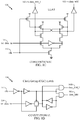
- the data inputs to self-clocked write bitline driver 100 are self-clocked data signals represented as true and complement phase-clocks, data_wbl 102a and data_wbl_1 102b. These true and complement phase-clocks, data wbl 102a and data_wbl_1 102b can be generated by an input interface such as an entry latch (ELAT) or differential clock-gating latch, which are further described in FIGS. 1C-D .
- ELAT entry latch
- differential clock-gating latch differential clock-gating latch
- the true and complement phase-clocks, data_wbl 102a and data_wbl_1 102b can pass through inverters 104a and 104b respectively to generate inverted true and complement data input signals d_wbl_1 103a and d wbl 103b to self-clocked write bitline driver 100.
- the self-clocked write bitline driver 100 comprises a first complementary MOS (CMOS) structure including PMOS 106a and NMOS 108a, and a second CMOS structure comprising PMOS 106b and NMOS 108b. As shown in FIG.
- CMOS complementary MOS
- data_wbl 102a is connected to the gate of NMOS 108b and data_wbl_1 102b is connected to the gate of NMOS 108a.
- the corresponding inverted signals are connected to the PMOS gates, such that d wbl 103b is connected to the gate of PMOS 106b and d_wbl_1 103a is connected to the gate of PMOS 106a.
- the outputs of the self-clocked write bitline driver 100 are available from the outputs of the two CMOS structures, as wbl 110a and wbl_1 110b.
- Clock 112 is a system clock. In this illustration, no active writes are shown during the low phase of clock 112. In the first cycle, starting from the left, a low phase of clock 112 is shown. During the low phase of clock 112, outputs write bitlines wbl 110a and wbl w 110b are not driven, or are floated, since both the true and the complement phase-clocks data_wbl 102a and data_wbl_1 102b, are at a low phase or binary value "0,” thus turning off NMOS 108a, 108b, as well as PMOS 106a, 106b.
- phase-clock data_wbl 102a and data_wbl_1 102b inputs will switch high while the other remains low or at zero.
- phase-clock data_wbl 102a will switch high while data_wbl_1 102b remains low.
- phase-clock data_wbl 102a will be low while data_wbl_1 102b switches high.
- one of the inverted signals d_wbl_1 103a and d_wbl 103b will switch low while the other remains high.
- data_wbl 102a switches high or to "1," which enables NMOS 108b to be switched on, and thus pulling output wbl_1 110b low or to "0.”
- the corresponding inverted signal d_wbl_1 103a switches low to turn on PMOS 106a, which drives output wbl 110a high.
- ELAT 120 which may be used to generate the true and the complement phase-clocks data_wbl 102a and data_wbl_1 102b of FIGS. 1A and 1B is illustrated.
- the operation of ELAT 120 may be according to well-known implementations of entry latch structures as will be understood by one skilled in the art, and thus, an exhaustive explanation of the structure and working of ELAT 120 will be avoided.
- the data value to be written to a bit cell using self-clocked write bitline driver 100 can be provided on data input signal wr_data_in 114.
- System clock 112 is another input to ELAT 120.
- ELAT 120 can generate the self-clocked true and the complement phase-clocks data_wbl 102a and data_wbl_1 102b which are input to self-clocked write bitline driver 100 of FIG. 1B .
- clock gating (CGC) latch 130 which may alternatively be used to generate the true and the complement phase-clocks data wbl 102a and data_wbl_1 102b of FIGS. 1A and 1B is illustrated.
- the operation of CGC latch 130 may also be according to well-known implementations of CGC latch structures as will be understood by one skilled in the art, and thus, an exhaustive explanation of the structure and working of CGC latch 130 will be avoided.
- the data value to be written to a bit cell using self-clocked write bitline driver 100 can be provided on data input signal wr_data_in 114.
- System clock 112 is another input to CGC latch 130.
- CGC latch 130 can generate the self-clocked true and the complement phase-clocks data wbl 102a and data_wbl_1 102b which are input to self-clocked write bitline driver 100 of FIG. 1B .
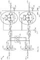
- FIG. 2A illustrates circuit 200 for efficient voltage shifting of differential signals between voltage domains, as applied to an exemplary case for self-clocked write bitline drivers described previously.
- FIG. 2A illustrates circuit 200 for efficient voltage shifting of differential signals between voltage domains, as applied to an exemplary case for self-clocked write bitline drivers described previously.
- circuit 200 are not so limited, but can be extended to any voltage shifting circuitry for shifting differential signals (i.e., signals presented in a true and complement form) from a first voltage domain to a second voltage domain.
- Circuit 200 can be used for avoiding skew issues and impacts of supply voltage variations across voltage domains for differential signals, particularly, for differential signals which are of a self-clocked nature or of a return-to-zero (RTZ) type.
- exemplary circuit 200 can involve two level shifters, one each for the true and the complement signals of the differential signals, which eliminates the aforementioned issues with conventional voltage shifting. Additional aspects and features of circuit 200 will now be described with regard to the example of shifting true and complement differential signals, data t 202a and data_c 202b (which may be similar to true and complement phase-clocks, data_wbl 102a and data_wbl_1 102b of FIG. 1B when applied in the context of write bitline drivers).
- circuit 200 represents a schematic circuit diagram for a voltage shifting circuit for shifting differential signals between two voltage domains representatively shown as vddx 230 and vddar 240.
- circuit 200 accepts differential signal inputs from the first voltage domain vddx 230, and converts them to differential signal outputs in the second voltage domain vddar 240.
- the second voltage domain vddar 240 may be a voltage island which has a voltage supply corresponding to the voltage supply to the memory array.
- circuit 200 may provide write assistance to the write bitline drivers operating on a memory array contained within the voltage island.
- the first and second voltage domain may have different voltage supplies or different levels of supply voltages, where a first supply voltage of the first voltage domain may be less than or greater than a second supply voltage of the second voltage domain.
- self-clocked true and complement data input signals are input to circuit 200 at the first voltage domain vddx 230.
- These data input signals pass through inverters 204a and 204b situated within the first voltage domain vddx 230, and generate the corresponding inverted signals data_t_1 203a and data_c_1 203b respectively.
- the two pairs of data input signals and corresponding inverted signals i.e., data t 202a, data_t_1 203a and data_c 202b, data_c_1 203b are input to two parallel and separate full voltage level shifters 220a and 220b respectively in the second voltage domain vddar 240.
- first and second full voltage level shifters 220a and 220b are used as above, in contrast to a conventional single voltage shifter. This avoids skew issues with supply variation across the two voltage domains because the data input signals are self-clocked (e.g., based on ELAT 120 or CGC latch 130 as in FIGS. 1C-D ).
- the two voltage level shifters 220a and 220b are configured to shift signals from the first voltage domain vddx 230 to the second voltage domain vddar 240.
- a detailed operation and functionality of the voltage level shifters 220a and 220b will be avoided herein as they may be designed according to conventional approaches which will be known by one skilled in the art.
- the two full level shifters 220a and 220b provide voltage level shifted self-clocked intermediate signals data_t_1_lvs 205a and data_c_1_lvs 205b in the second voltage domain vddar 240, corresponding to the inverted differential signals data_t_1 203a and data_c_1 203b in the first voltage domain vddx 230.
- circuit 200 may further employ the clamp signal, clamp_vddar 213 in the second voltage domain vddar 240 (e.g., coupled to PMOS head switches in the full level shifters 220a and 220b) in order to prevent crow-bar current.
- the clamp signal clamp_vddar 213 may be active high or active low depending on specific implementations and operates to prevent unwanted crow-bar or short circuit current from being generated when the first voltage supply to the first voltage domain vddx 230 is collapsed (e.g., for power saving when no write operation is in progress).
- clamp_vddar 213 is also coupled with voltage level shifted outputs data_t_1_lvs 205a and data_c_1_lvs 205b of the full level shifters 220a and 220b by means of NOR gates 222a and 222b respectively, which ensures that output write bitline signals of circuit 200, wbl_1_vddar 210b and wbl_vddar 210a, are floating on the active second voltage domain vddar 240 when the first voltage domain vddx 230 is collapsed.
- the output write bitline signals wbl_1_vddar 210b and wbl_vddar 210a are "tristated" in order to allow their values to float when the first voltage domain vddx 230 is collapsed.
- Outputs of NOR gates 222a and 222b i.e., outputs of data_t_l_lvs 205a and data_c_l_lvs 205b of the full level shifters 220a and 220b clamped with clamp vddar 213 are provided on signals data_t_vddar 214a and data_c_vddar 214b respectively.
- signals data_t_vddar 214a and data_c_vddar 214b in the second voltage domain vddar 240 are derived from inputs data_wb1 102a and data_wb1_1 102b of self-clocked write bitline driver 100 of FIG. 1B , without use of an input clock signal.
- the tristated output write bitline signals wbl_l_vddar 210b and wbl_vddar 210a are also self-clocked. Therefore, the output write bitline signals wbl_1_vddar 210b and wbl_vddar 210a may also be referred to herein as "voltage level shifted self-clocked tristated true and complement output signals" of circuit 200.
- Circuit 200 also comprises a CMOS circuit 207a comprising PMOS 206a and NMOS 208a, and another CMOS circuit 207b comprising PMOS 206b and NMOS 208b, which provide tristating logic for tristating outputs of circuit 200.
- data_t_vddar 214a is connected to the gate of NMOS 208b and data_c_vddar 214b is connected to the gate of NMOS 208a.
- the corresponding inverted signals are connected to the PMOS gates, such that data_c_l_vddar 211b is connected to the gate of PMOS 206b and data_t_1_vddar 211a is connected to the gate of PMOS 206a.
- the outputs of the circuit 200 are available from the outputs of the two CMOS circuits 207a and 207b, as the tristated self-clocked level shifted differential signals wbl_l_vaddr 210b and wbl_vaddr 210a, as shown.
- These level shifted differential output signals of circuit 200 may be used to write bit cells of a memory array (not shown), with write assistance derived from the level shifting to the second voltage domain vddar 240.
- Time instances t1, t2, t3, and t4 mark the start of successive clock periods of a system clock used in the self-clocking of the signals illustrated.
- Signals in FIG. 2A are shown to be of high or logic level "1,” logic low or logic level “0,” or floating or at an unknown (X) value between these two levels.
- a low phase of the clamp signal clamp_vaddr 213 is illustrated, wherein the true part of the differential data input signals.
- Data input signal data_t 202a is switched high or to logic level "1" at the first instance t1.
- the complement data input signal data_c 202b remains low or "0" at time t1.
- the inverted signals dta_t_1_lvs 205a and data_c_1_lvs 205b are driven to "0" and "1," in the second voltage domain vdd_ar 240.
- the signals data_t_vddar 214a and data_c_1_vddar 211b are thus driven to "1" and "1" in the second voltage domain vdd_ar 240 at time t1.
- This causes the output signal wbl_1_vddar 210b to be driven to "0.”
- data_c_vddar 214b and data_t_1_vddar 211a being at "0" and "0" values, respectively, causes output signal wbl_vddar 210a to be driven to "1.”
- the output signals of circuit 200 are based on a first edge (e.g., the rising edge of the true data input signal data_t 202a) at time t1, which makes the first edge timing critical for the output signals.
- Time instances t3 and t4 represent a phase where the first voltage domain vddr 230 is collapsed (e.g., when no write operation is being performed), which drives true and complement data input signals data_t 202a and data c 202b to be driven to unknown states "X.”
- clamp signal clamp_vddar 213 is driven high, which protects the signals in the second voltage domain vddar 240 from crow-bar currents, race conditions, short circuits, etc.
- CMOS circuits 207a and 207b are turned off, providing the requisite tristating logic or circuitry for floating the self-clocked output signals wbl_vddar 210a and wbl_1_vddar 210b. Since, output signals wbl vddar 210a and wbl_1_vddar 210b are caused to float, the write bitlines that these signals may be used to drive are floated, thus conserving leakage power in the memory array.
- an exemplary aspect can include a method (300) of operating a circuit (e.g., circuit 200), the method comprising: inputting self-clocked differential input signals comprising self-clocked true and complement data input signals (e.g., data t 202a and data_c 202b) to the circuit in a first voltage domain (e.g., vddx 230) - Block 302; generating voltage level shifted self-clocked intermediate true and complement signals (e.g., data_t_l_lvs 205a and data_c_l_lvs 205b) in a second voltage domain (e.g., vddar 240) from the self-clocked true and complement data input signals in the first voltage domain, using first and second full voltage level shifters (e.g., 220a and 220b) - Block 304; and generating voltage level
- Wireless device 400 includes processor 464 coupled to memory 432.
- Wireless device 400 is also shown to include exemplary circuit 200 illustrated in FIG. 2A , where circuit 200 may provide voltage shifting of differential data signals provided by processor 464 in a first voltage domain vddx 230, to self-clocked differential write bitline driver output signals in a second voltage domain vddar 240.
- One or more arrays of bit cells in memory 432 may be configured in a voltage island corresponding to the second voltage domain vddar 240.
- Circuit 200 is shown to representatively straddle the two voltage domains 230 and 240 in FIG. 4 , but it will be understood that this is merely for schematically representing aspects of this disclosure and not to be construed as a limitation in the placement/routing of hardware blocks pertaining to circuit 200.
- FIG. 4 also shows display controller 426 that is coupled to processor 464 and to display 428.
- Coder/decoder (CODEC) 434 e.g., an audio and/or voice CODEC
- Other components such as wireless controller 440 (which may include a modem) are also illustrated.
- Speaker 436 and microphone 438 can be coupled to CODEC 434.
- FIG. 4 also indicates that wireless controller 440 can be coupled to wireless antenna 442.
- processor 464, display controller 426, memory 432, CODEC 434, and wireless controller 440 are included in a system-in-package or system-on-chip device 422.
- input device 430 and power supply 444 are coupled to the system-on-chip device 422.
- display 428, input device 430, speaker 436, microphone 438, wireless antenna 442, and power supply 444 are external to the system-on-chip device 422.
- each of display 428, input device 430, speaker 436, microphone 438, wireless antenna 442, and power supply 444 can be coupled to a component of the system-on-chip device 422, such as an interface or a controller.
- FIG. 4 depicts a wireless communications device, processor 464, and memory 432 may also be integrated into a set-top box, a music player, a video player, an entertainment unit, a navigation device, a personal digital assistant (PDA), a fixed location data unit, a mobile phone, a smart phone, or a computer.
- PDA personal digital assistant
- a software module may reside in RAM memory, flash memory, ROM memory, EPROM memory, EEPROM memory, registers, hard disk, a removable disk, a CD-ROM, or any other form of storage medium known in the art.
- An exemplary storage medium is coupled to the processor such that the processor can read information from, and write information to, the storage medium. In the alternative, the storage medium may be integral to the processor.
- an embodiment of the invention can include a computer readable media embodying a method for operating a multiprocessing system with disunited private-information and shared-information caches. Accordingly, the invention is not limited to illustrated examples and any means for performing the functionality described herein are included in embodiments of the invention.
Landscapes
- Engineering & Computer Science (AREA)
- Microelectronics & Electronic Packaging (AREA)
- Computer Hardware Design (AREA)
- Power Engineering (AREA)
- Static Random-Access Memory (AREA)
- Logic Circuits (AREA)
Claims (14)
- Eine Vorrichtung, die aufweist:erste und zweite Vollspannungspegelverschieber (220a, 220b), die jeweils konfiguriert sind zum Empfangen von selbstgetakteten wahren (202a) und komplementären (202b) Dateneingabesignalen in einer ersten Spannungsdomäne und zum Erzeugen von entsprechenden spannungspegelverschobenen, selbstgetakteten wahren (205a) und komplementären (205b) Zwischensignalen in einer zweiten Spannungsdomäne basierend auf den selbstgetakteten wahren und komplementären Dateneingabesignalen in der ersten Spannungsdomäne,erste (207a) und zweite (207b) komplementäre Metalloxidhalbleiter (CMOS)-Schaltkreise, die konfiguriert sind zum Erzeugen von spannungspegelverschobenen, selbstgetakteten wahren (210b) und komplementären (210a) Dreizustand-Ausgabesignalen in der zweiten Spannungsdomäne basierend auf den spannungspegelverschobenen, selbstgetakteten wahren und komplementären Zwischensignalen, undeinen Klemmschaltkreis in der zweiten Spannungsdomäne, der aufweist:ein erstes NOR-Gatter (222a) mit dem spannungspegelverschobenen, selbstgetakteten wahren Zwischensignal (205a) und einem Klemmsignal (213) als Eingaben, wobei eine Ausgabe des ersten NOR-Gatters (222a) mit einem Gate einer zweiten n-Kanal-MOS (NMOS)-Einrichtung (208b) des zweiten CMOS-Schaltkreises (207b) gekoppelt ist und der Kehrwert der Ausgabe des ersten NOR-Gatters mit einem Gate einer ersten p-Kanal-MOS (PMOS)-Einrichtung (206a) des ersten CMOS-Schaltkreises (207a) gekoppelt ist, undein zweites NOR-Gatter (222b) mit dem spannungspegelverschobenen, selbstgetakteten komplementären Zwischensignal (205b) und dem Klemmsignal (213) als Eingaben, wobei eine Ausgabe des zweiten NOR-Gatters mit einem Gate einer ersten n-Kanal MOS (NMOS)-Einrichtung des ersten CMOS-Schaltkreises gekoppelt ist und ein Kehrwert der Ausgabe des zweiten NOR-Gatters mit einem Gate einer zweiten p-Kanal-MOS (PMOS)-Einrichtung (206b) des zweiten CMOS-Schaltkreises gekoppelt ist,wobei die Klemmschaltung konfiguriert ist zum Schwebenlassen der spannungspegelverschobenen, selbstgetakteten wahren und komplementären Dreizustand-Ausgabesignale (210b, 210a), wenn das Klemmsignal hoch ist.
- Vorrichtung nach Anspruch 1, die mit einem Speicherarray (432) in der zweiten Spannungsdomäne gekoppelt ist.
- Vorrichtung nach Anspruch 2, wobei die spannungspegelverschobenen, selbstgetakteten wahren und komplementären Dreizustand-Ausgabesignale (210b, 210a) in der zweiten Spannungsdomäne konfiguriert sind zum Treiben von Schreib-Bitleitungen für das Beschreiben von Speicherbitzellen in dem Speicherarray in der zweiten Spannungsdomäne.
- Vorrichtung nach Anspruch 1, wobei der Crowbarstrom in den ersten und zweiten Vollspannungspegelverschiebern durch die Klemmschaltung verhindert wird, wenn das Klemmsignal hoch ist.
- Vorrichtung nach Anspruch 1, wobei die selbstgetakteten wahren und komplementären Dateneingabesignale auf einem Dateneingabesignal und einem Systemtakt basieren.
- Vorrichtung nach Anspruch 1, wobei die selbstgetakteten wahren und komplementären Dateneingabesignale (202a, 202b) von einem Eintrittslatch oder einem Taktgatterlatch erzeugt werden.
- Vorrichtung nach Anspruch 1, wobei die selbstgetakteten wahren und komplementären Dateneingabesignale (202a, 202b) RZ (Return-to-Zero) oder selbstrückstellende Signale sind.
- Vorrichtung nach Anspruch 1, die in einem Gerät integriert ist, das aus der Gruppe ausgewählt ist, die eine Set-Top-Box, ein Musikwiedergabegerät, ein Videowiedergabegerät, eine Unterhaltungseinheit, ein Navigationsgerät, ein Kommunikationsgerät, einen PDA, eine fest positionierte Dateneinheit, ein Mobiltelefon und einen Computer umfasst.
- Ein Verfahren zum Betreiben eines Schaltkreises, wobei das Verfahren aufweist:Empfangen von selbstgetakteten wahren und komplementären Dateneingabesignalen (202a, 202b) durch die Schaltung in einer ersten Spannungsdomäne,Erzeugen von spannungspegelverschobenen, selbstgetakteten wahren und komplementären Zwischensignalen (205a, 205b) in einer zweiten Spannungsdomäne jeweils aus den selbstgetakteten wahren und komplementären Dateneingabesignalen in der ersten Spannungsdomäne unter Verwendung von ersten und zweiten Vollspannungspegelverschiebern,Erzeugen von spannungspegelverschobenen, selbstgetakteten wahren und komplementären Dreizustand-Ausgabesignalen (210b, 210a) in der zweiten Spannungsdomäne jeweils aus den spannungspegelverschobenen, selbstgetakteten wahren und komplementären Zwischensignalen unter Verwendung von ersten und zweiten komplementären Metalloxidhalbleiter (CMOS)-Schaltkreisen, undSchwebenlassen der spannungspegelverschobenen, selbstgetakteten wahren und komplementären Dreizustand-Ausgabesignale (210b, 210a), wenn ein mit einer Klemmschaltung gekoppeltes Klemmsignal hoch ist, wobei die Klemmschaltung aufweist:ein erstes NOR-Gatter (222a) mit dem spannungspegelverschobenen, selbstgetakteten wahren Zwischensignal (205a) und einem Klemmsignal (213) als Eingaben, wobei eine Ausgabe des ersten NOR-Gatters mit einem Gate einer zweiten n-Kanal-MOS (NMOS)-Einrichtung (208b) des zweiten CMOS-Schaltkreises (207b) gekoppelt ist und der Kehrwert der Ausgabe des ersten NOR-Gatters mit einem Gate einer ersten p-Kanal-MOS (PMOS)-Einrichtung (206a) des ersten CMOS-Schaltkreises (207a) gekoppelt ist, undein zweites NOR-Gatter (222b) mit dem spannungspegelverschobenen, selbstgetakteten komplementären Zwischensignal (205b) und dem Klemmsignal (213) als Eingaben, wobei eine Ausgabe des zweiten NOR-Gatters (222b) mit einem Gate einer ersten n-Kanal MOS (NMOS)-Einrichtung (208a) des ersten CMOS-Schaltkreises gekoppelt ist und ein Kehrwert der Ausgabe des zweiten NOR-Gatters mit einem Gate einer zweiten p-Kanal-MOS (PMOS)-Einrichtung (206b) des zweiten CMOS-Schaltkreises gekoppelt (207b) ist.
- Verfahren nach Anspruch 9, das weiterhin das Vorsehen der spannungspegelverschobenen, selbstgetakteten wahren und komplementären Dreizustand-Ausgabesignale (210b, 210a) in der zweiten Spannungsdomäne zum Treiben von Schreib-Bitleitungen für das Beschreiben von Speicherbitzellen in einem Speicherarray (432) in der zweiten Spannungsdomäne aufweist.
- Verfahren nach Anspruch 9, das weiterhin das Verhindern, durch die Klemmschaltung, eines Crowbarstroms in den ersten und zweiten Vollspannungspegelverschiebern (220a, 220b), wenn das Klemmsignal hoch ist, aufweist.
- Verfahren nach Anspruch 9, das weiterhin das Erzeugen der selbstgetakteten wahren und komplementären Dateneingabesignale (202a, 202b) basierend auf einem Dateneingabesignal und einem Systemtakt aufweist.
- Verfahren nach Anspruch 9, das weiterhin das Erzeugen der selbstgetakteten wahren und komplementären Dateneingabesignale (202a, 202b) unter Verwendung eines Eintrittslatches oder eines Taktgatterlatches aufweist.
- Verfahren nach Anspruch 9, wobei die selbstgetakteten wahren und komplementären Dateneingabesignale RZ (Return-to-Zero)- oder selbstrückstellende Signale sind.
Applications Claiming Priority (2)
| Application Number | Priority Date | Filing Date | Title |
|---|---|---|---|
| US14/499,035 US9378789B2 (en) | 2014-09-26 | 2014-09-26 | Voltage level shifted self-clocked write assistance |
| PCT/US2015/049220 WO2016048660A1 (en) | 2014-09-26 | 2015-09-09 | Voltage level shifted self-clocked write assistance |
Publications (2)
| Publication Number | Publication Date |
|---|---|
| EP3198609A1 EP3198609A1 (de) | 2017-08-02 |
| EP3198609B1 true EP3198609B1 (de) | 2018-11-21 |
Family
ID=54199294
Family Applications (1)
| Application Number | Title | Priority Date | Filing Date |
|---|---|---|---|
| EP15770996.5A Active EP3198609B1 (de) | 2014-09-26 | 2015-09-09 | Spannungspegelverschobene selbstgetaktete schreibunterstützung |
Country Status (4)
| Country | Link |
|---|---|
| US (1) | US9378789B2 (de) |
| EP (1) | EP3198609B1 (de) |
| CN (1) | CN106716535B (de) |
| WO (1) | WO2016048660A1 (de) |
Families Citing this family (8)
| Publication number | Priority date | Publication date | Assignee | Title |
|---|---|---|---|---|
| US9625938B2 (en) * | 2015-03-25 | 2017-04-18 | Advanced Micro Devices, Inc. | Integrated differential clock gater |
| US10755770B2 (en) * | 2016-09-30 | 2020-08-25 | Taiwan Semiconductor Manufacturing Company, Ltd. | Circuit and method for writing to a bit cell |
| DE102017117791B4 (de) * | 2016-09-30 | 2025-06-12 | Taiwan Semiconductor Manufacturing Co. Ltd. | Schaltung und Verfahren zum Schreiben auf eine Bitzelle |
| US9911472B1 (en) | 2016-11-28 | 2018-03-06 | Qualcomm Incorporated | Write bitline driver for a dual voltage domain |
| US10607671B2 (en) * | 2018-02-17 | 2020-03-31 | Micron Technology, Inc. | Timing circuit for command path in a memory device |
| US10762934B2 (en) * | 2018-06-28 | 2020-09-01 | Taiwan Semiconductor Manufacturing Co., Ltd. | Leakage pathway prevention in a memory storage device |
| DE102020123265A1 (de) | 2019-09-30 | 2021-04-01 | Taiwan Semiconductor Manufacturing Co., Ltd. | Speichervorrichtung mit globalen und lokalen Latches |
| US11361818B2 (en) * | 2019-09-30 | 2022-06-14 | Taiwan Semiconductor Manufacturing Company, Ltd. | Memory device with global and local latches |
Family Cites Families (24)
| Publication number | Priority date | Publication date | Assignee | Title |
|---|---|---|---|---|
| JPS566525A (en) | 1979-06-29 | 1981-01-23 | Hitachi Ltd | 2-phase clock pulse generating circuit |
| US4380080A (en) | 1980-12-30 | 1983-04-12 | Sperry Corporation | Tri-level differential line receiver |
| US5144162A (en) * | 1990-07-13 | 1992-09-01 | Texas Instruments Incorporated | High speed signal driving scheme |
| US5202855A (en) | 1991-01-14 | 1993-04-13 | Motorola, Inc. | DRAM with a controlled boosted voltage level shifting driver |
| KR960001860B1 (ko) * | 1993-06-05 | 1996-02-06 | 삼성전자주식회사 | 반도체집적회로의 데이타 입출력선 센싱회로 |
| US5811990A (en) | 1993-10-15 | 1998-09-22 | Micron Technology, Inc. | Voltage pump and a level translator circuit |
| US5729160A (en) | 1994-07-20 | 1998-03-17 | Mosaid Technologies Incorporated | Self-timed circuit control device and method |
| US5550488A (en) | 1995-06-06 | 1996-08-27 | International Business Machines Corporation | Self timed driver |
| US5767716A (en) | 1995-09-26 | 1998-06-16 | Texas Instruments Incorporated | Noise insensitive high performance energy efficient push pull isolation flip-flop circuits |
| US5809528A (en) | 1996-12-24 | 1998-09-15 | International Business Machines Corporation | Method and circuit for a least recently used replacement mechanism and invalidated address handling in a fully associative many-way cache memory |
| US5933386A (en) | 1997-12-23 | 1999-08-03 | Mitsubishi Semiconductor America, Inc. | Driving memory bitlines using boosted voltage |
| JP3796034B2 (ja) * | 1997-12-26 | 2006-07-12 | 株式会社ルネサステクノロジ | レベル変換回路および半導体集積回路装置 |
| US6069839A (en) | 1998-03-20 | 2000-05-30 | Cypress Semiconductor Corp. | Circuit and method for implementing single-cycle read/write operation(s), and random access memory including the circuit and/or practicing the method |
| US6483363B1 (en) | 2000-09-15 | 2002-11-19 | Intel Corporation | Storage element with stock node capacitive load |
| DE102005063097B4 (de) | 2005-12-30 | 2014-09-04 | Infineon Technologies Ag | Gepulstes statisches Flip-Flop |
| DE102007006385B4 (de) | 2007-02-08 | 2019-02-14 | Infineon Technologies Ag | Eine Schaltkreis-Anordnung, ein Prozessor mit einer Schaltkreis-Anordnung, ein elektrisches Gerät und ein Verfahren zum Betreiben einer Schaltkreis-Anordnung |
| US8184492B2 (en) * | 2009-01-09 | 2012-05-22 | Micron Technology, Inc. | Tri-state driver circuits having automatic high-impedance enabling |
| US8120968B2 (en) | 2010-02-12 | 2012-02-21 | International Business Machines Corporation | High voltage word line driver |
| US8456929B2 (en) * | 2010-04-07 | 2013-06-04 | Qualcomm Incorporated | Circuits, systems, and methods for dynamic voltage level shifting |
| KR101787758B1 (ko) * | 2011-06-09 | 2017-10-19 | 매그나칩 반도체 유한회사 | 레벨 쉬프터 |
| CN103178829B (zh) * | 2011-12-20 | 2015-11-25 | 中芯国际集成电路制造(上海)有限公司 | 电平移位电路 |
| US8854902B2 (en) | 2012-05-18 | 2014-10-07 | Stmicroelectronics International N.V. | Write self timing circuitry for self-timed memory |
| US8976607B2 (en) | 2013-03-05 | 2015-03-10 | Qualcomm Incorporated | High-speed memory write driver circuit with voltage level shifting features |
| US9536578B2 (en) | 2013-03-15 | 2017-01-03 | Qualcomm Incorporated | Apparatus and method for writing data to memory array circuits |
-
2014
- 2014-09-26 US US14/499,035 patent/US9378789B2/en not_active Expired - Fee Related
-
2015
- 2015-09-09 CN CN201580049972.2A patent/CN106716535B/zh active Active
- 2015-09-09 WO PCT/US2015/049220 patent/WO2016048660A1/en not_active Ceased
- 2015-09-09 EP EP15770996.5A patent/EP3198609B1/de active Active
Non-Patent Citations (1)
| Title |
|---|
| None * |
Also Published As
| Publication number | Publication date |
|---|---|
| US20160093346A1 (en) | 2016-03-31 |
| WO2016048660A1 (en) | 2016-03-31 |
| EP3198609A1 (de) | 2017-08-02 |
| CN106716535B (zh) | 2019-02-15 |
| CN106716535A (zh) | 2017-05-24 |
| US9378789B2 (en) | 2016-06-28 |
Similar Documents
| Publication | Publication Date | Title |
|---|---|---|
| EP3198609B1 (de) | Spannungspegelverschobene selbstgetaktete schreibunterstützung | |
| KR101564340B1 (ko) | 개선된 안정성 및 감소된 비트셀 사이즈를 갖는 저전력 5t sram | |
| US10115481B2 (en) | Read-assist circuits for memory bit cells employing a P-type field-effect transistor (PFET) read port(s), and related memory systems and methods | |
| US8638153B2 (en) | Pulse clock generation logic with built-in level shifter and programmable rising edge and pulse width | |
| US8488396B2 (en) | Dual rail static random access memory | |
| CN101582292B (zh) | 存储器电路与存储器电路操作方法 | |
| CN102148052B (zh) | 存储器电路及其控制电路装置 | |
| CN107077884B (zh) | 具有提供减少的读扰乱的传输门的七晶体管sram位单元 | |
| US8467263B2 (en) | Memory write operation methods and circuits | |
| US20150009751A1 (en) | Methods and systems to selectively boost an operating voltage of, and controls to an 8t bit-cell array and/or other logic blocks | |
| US8164938B2 (en) | Semiconductor memory device | |
| TW201447898A (zh) | 記憶體裝置以及在此種記憶體裝置中控制漏電流的方法 | |
| JP2009289308A (ja) | 半導体記憶装置 | |
| JP2015167058A (ja) | 半導体記憶装置 | |
| CN108231105A (zh) | 字线驱动器 | |
| JP2004355760A (ja) | データ記憶回路 | |
| US7420835B2 (en) | Single-port SRAM with improved read and write margins | |
| US20170194047A1 (en) | Integrated circuit including embedded memory device for performing dual-transient word line assist using triple power source and device having the same | |
| TW202303598A (zh) | 字線驅動器架構 | |
| US9911472B1 (en) | Write bitline driver for a dual voltage domain | |
| KR20060040968A (ko) | 반도체 메모리 장치의 차동 증폭기 제어회로 | |
| US20230410905A1 (en) | Split footer topology to improve vmin and leakage power for register file and read only memory designs | |
| KR20220165469A (ko) | 메모리 장치 및 메모리 장치의 동작 방법 | |
| WO2024207000A1 (en) | Selective source bias in memory periphery | |
| JP2010287266A (ja) | SRAM(StaticRandomAccessMemory)、及びSRAMへのアクセス方法 |
Legal Events
| Date | Code | Title | Description |
|---|---|---|---|
| STAA | Information on the status of an ep patent application or granted ep patent |
Free format text: STATUS: THE INTERNATIONAL PUBLICATION HAS BEEN MADE |
|
| PUAI | Public reference made under article 153(3) epc to a published international application that has entered the european phase |
Free format text: ORIGINAL CODE: 0009012 |
|
| STAA | Information on the status of an ep patent application or granted ep patent |
Free format text: STATUS: REQUEST FOR EXAMINATION WAS MADE |
|
| 17P | Request for examination filed |
Effective date: 20170214 |
|
| AK | Designated contracting states |
Kind code of ref document: A1 Designated state(s): AL AT BE BG CH CY CZ DE DK EE ES FI FR GB GR HR HU IE IS IT LI LT LU LV MC MK MT NL NO PL PT RO RS SE SI SK SM TR |
|
| AX | Request for extension of the european patent |
Extension state: BA ME |
|
| DAV | Request for validation of the european patent (deleted) | ||
| DAX | Request for extension of the european patent (deleted) | ||
| GRAP | Despatch of communication of intention to grant a patent |
Free format text: ORIGINAL CODE: EPIDOSNIGR1 |
|
| STAA | Information on the status of an ep patent application or granted ep patent |
Free format text: STATUS: GRANT OF PATENT IS INTENDED |
|
| RIC1 | Information provided on ipc code assigned before grant |
Ipc: G11C 11/419 20060101AFI20180619BHEP Ipc: G11C 7/12 20060101ALI20180619BHEP Ipc: G11C 5/14 20060101ALI20180619BHEP Ipc: H03K 3/356 20060101ALI20180619BHEP Ipc: G11C 7/10 20060101ALI20180619BHEP |
|
| INTG | Intention to grant announced |
Effective date: 20180704 |
|
| GRAS | Grant fee paid |
Free format text: ORIGINAL CODE: EPIDOSNIGR3 |
|
| GRAA | (expected) grant |
Free format text: ORIGINAL CODE: 0009210 |
|
| STAA | Information on the status of an ep patent application or granted ep patent |
Free format text: STATUS: THE PATENT HAS BEEN GRANTED |
|
| AK | Designated contracting states |
Kind code of ref document: B1 Designated state(s): AL AT BE BG CH CY CZ DE DK EE ES FI FR GB GR HR HU IE IS IT LI LT LU LV MC MK MT NL NO PL PT RO RS SE SI SK SM TR |
|
| REG | Reference to a national code |
Ref country code: CH Ref legal event code: EP |
|
| REG | Reference to a national code |
Ref country code: IE Ref legal event code: FG4D |
|
| REG | Reference to a national code |
Ref country code: DE Ref legal event code: R096 Ref document number: 602015020097 Country of ref document: DE |
|
| REG | Reference to a national code |
Ref country code: AT Ref legal event code: REF Ref document number: 1068476 Country of ref document: AT Kind code of ref document: T Effective date: 20181215 |
|
| REG | Reference to a national code |
Ref country code: NL Ref legal event code: MP Effective date: 20181121 |
|
| REG | Reference to a national code |
Ref country code: AT Ref legal event code: MK05 Ref document number: 1068476 Country of ref document: AT Kind code of ref document: T Effective date: 20181121 |
|
| PG25 | Lapsed in a contracting state [announced via postgrant information from national office to epo] |
Ref country code: BG Free format text: LAPSE BECAUSE OF FAILURE TO SUBMIT A TRANSLATION OF THE DESCRIPTION OR TO PAY THE FEE WITHIN THE PRESCRIBED TIME-LIMIT Effective date: 20190221 Ref country code: LT Free format text: LAPSE BECAUSE OF FAILURE TO SUBMIT A TRANSLATION OF THE DESCRIPTION OR TO PAY THE FEE WITHIN THE PRESCRIBED TIME-LIMIT Effective date: 20181121 Ref country code: FI Free format text: LAPSE BECAUSE OF FAILURE TO SUBMIT A TRANSLATION OF THE DESCRIPTION OR TO PAY THE FEE WITHIN THE PRESCRIBED TIME-LIMIT Effective date: 20181121 Ref country code: HR Free format text: LAPSE BECAUSE OF FAILURE TO SUBMIT A TRANSLATION OF THE DESCRIPTION OR TO PAY THE FEE WITHIN THE PRESCRIBED TIME-LIMIT Effective date: 20181121 Ref country code: LV Free format text: LAPSE BECAUSE OF FAILURE TO SUBMIT A TRANSLATION OF THE DESCRIPTION OR TO PAY THE FEE WITHIN THE PRESCRIBED TIME-LIMIT Effective date: 20181121 Ref country code: ES Free format text: LAPSE BECAUSE OF FAILURE TO SUBMIT A TRANSLATION OF THE DESCRIPTION OR TO PAY THE FEE WITHIN THE PRESCRIBED TIME-LIMIT Effective date: 20181121 Ref country code: AT Free format text: LAPSE BECAUSE OF FAILURE TO SUBMIT A TRANSLATION OF THE DESCRIPTION OR TO PAY THE FEE WITHIN THE PRESCRIBED TIME-LIMIT Effective date: 20181121 Ref country code: IS Free format text: LAPSE BECAUSE OF FAILURE TO SUBMIT A TRANSLATION OF THE DESCRIPTION OR TO PAY THE FEE WITHIN THE PRESCRIBED TIME-LIMIT Effective date: 20190321 Ref country code: NO Free format text: LAPSE BECAUSE OF FAILURE TO SUBMIT A TRANSLATION OF THE DESCRIPTION OR TO PAY THE FEE WITHIN THE PRESCRIBED TIME-LIMIT Effective date: 20190221 |
|
| PG25 | Lapsed in a contracting state [announced via postgrant information from national office to epo] |
Ref country code: GR Free format text: LAPSE BECAUSE OF FAILURE TO SUBMIT A TRANSLATION OF THE DESCRIPTION OR TO PAY THE FEE WITHIN THE PRESCRIBED TIME-LIMIT Effective date: 20190222 Ref country code: PT Free format text: LAPSE BECAUSE OF FAILURE TO SUBMIT A TRANSLATION OF THE DESCRIPTION OR TO PAY THE FEE WITHIN THE PRESCRIBED TIME-LIMIT Effective date: 20190321 Ref country code: SE Free format text: LAPSE BECAUSE OF FAILURE TO SUBMIT A TRANSLATION OF THE DESCRIPTION OR TO PAY THE FEE WITHIN THE PRESCRIBED TIME-LIMIT Effective date: 20181121 Ref country code: NL Free format text: LAPSE BECAUSE OF FAILURE TO SUBMIT A TRANSLATION OF THE DESCRIPTION OR TO PAY THE FEE WITHIN THE PRESCRIBED TIME-LIMIT Effective date: 20181121 Ref country code: RS Free format text: LAPSE BECAUSE OF FAILURE TO SUBMIT A TRANSLATION OF THE DESCRIPTION OR TO PAY THE FEE WITHIN THE PRESCRIBED TIME-LIMIT Effective date: 20181121 Ref country code: AL Free format text: LAPSE BECAUSE OF FAILURE TO SUBMIT A TRANSLATION OF THE DESCRIPTION OR TO PAY THE FEE WITHIN THE PRESCRIBED TIME-LIMIT Effective date: 20181121 |
|
| PG25 | Lapsed in a contracting state [announced via postgrant information from national office to epo] |
Ref country code: PL Free format text: LAPSE BECAUSE OF FAILURE TO SUBMIT A TRANSLATION OF THE DESCRIPTION OR TO PAY THE FEE WITHIN THE PRESCRIBED TIME-LIMIT Effective date: 20181121 Ref country code: IT Free format text: LAPSE BECAUSE OF FAILURE TO SUBMIT A TRANSLATION OF THE DESCRIPTION OR TO PAY THE FEE WITHIN THE PRESCRIBED TIME-LIMIT Effective date: 20181121 Ref country code: CZ Free format text: LAPSE BECAUSE OF FAILURE TO SUBMIT A TRANSLATION OF THE DESCRIPTION OR TO PAY THE FEE WITHIN THE PRESCRIBED TIME-LIMIT Effective date: 20181121 Ref country code: DK Free format text: LAPSE BECAUSE OF FAILURE TO SUBMIT A TRANSLATION OF THE DESCRIPTION OR TO PAY THE FEE WITHIN THE PRESCRIBED TIME-LIMIT Effective date: 20181121 |
|
| REG | Reference to a national code |
Ref country code: DE Ref legal event code: R097 Ref document number: 602015020097 Country of ref document: DE |
|
| PG25 | Lapsed in a contracting state [announced via postgrant information from national office to epo] |
Ref country code: SK Free format text: LAPSE BECAUSE OF FAILURE TO SUBMIT A TRANSLATION OF THE DESCRIPTION OR TO PAY THE FEE WITHIN THE PRESCRIBED TIME-LIMIT Effective date: 20181121 Ref country code: SM Free format text: LAPSE BECAUSE OF FAILURE TO SUBMIT A TRANSLATION OF THE DESCRIPTION OR TO PAY THE FEE WITHIN THE PRESCRIBED TIME-LIMIT Effective date: 20181121 Ref country code: EE Free format text: LAPSE BECAUSE OF FAILURE TO SUBMIT A TRANSLATION OF THE DESCRIPTION OR TO PAY THE FEE WITHIN THE PRESCRIBED TIME-LIMIT Effective date: 20181121 Ref country code: RO Free format text: LAPSE BECAUSE OF FAILURE TO SUBMIT A TRANSLATION OF THE DESCRIPTION OR TO PAY THE FEE WITHIN THE PRESCRIBED TIME-LIMIT Effective date: 20181121 |
|
| PLBE | No opposition filed within time limit |
Free format text: ORIGINAL CODE: 0009261 |
|
| STAA | Information on the status of an ep patent application or granted ep patent |
Free format text: STATUS: NO OPPOSITION FILED WITHIN TIME LIMIT |
|
| 26N | No opposition filed |
Effective date: 20190822 |
|
| PG25 | Lapsed in a contracting state [announced via postgrant information from national office to epo] |
Ref country code: SI Free format text: LAPSE BECAUSE OF FAILURE TO SUBMIT A TRANSLATION OF THE DESCRIPTION OR TO PAY THE FEE WITHIN THE PRESCRIBED TIME-LIMIT Effective date: 20181121 |
|
| PG25 | Lapsed in a contracting state [announced via postgrant information from national office to epo] |
Ref country code: TR Free format text: LAPSE BECAUSE OF FAILURE TO SUBMIT A TRANSLATION OF THE DESCRIPTION OR TO PAY THE FEE WITHIN THE PRESCRIBED TIME-LIMIT Effective date: 20181121 |
|
| PG25 | Lapsed in a contracting state [announced via postgrant information from national office to epo] |
Ref country code: MC Free format text: LAPSE BECAUSE OF FAILURE TO SUBMIT A TRANSLATION OF THE DESCRIPTION OR TO PAY THE FEE WITHIN THE PRESCRIBED TIME-LIMIT Effective date: 20181121 |
|
| REG | Reference to a national code |
Ref country code: CH Ref legal event code: PL |
|
| PG25 | Lapsed in a contracting state [announced via postgrant information from national office to epo] |
Ref country code: LU Free format text: LAPSE BECAUSE OF NON-PAYMENT OF DUE FEES Effective date: 20190909 Ref country code: LI Free format text: LAPSE BECAUSE OF NON-PAYMENT OF DUE FEES Effective date: 20190930 Ref country code: IE Free format text: LAPSE BECAUSE OF NON-PAYMENT OF DUE FEES Effective date: 20190909 Ref country code: CH Free format text: LAPSE BECAUSE OF NON-PAYMENT OF DUE FEES Effective date: 20190930 |
|
| REG | Reference to a national code |
Ref country code: BE Ref legal event code: MM Effective date: 20190930 |
|
| PG25 | Lapsed in a contracting state [announced via postgrant information from national office to epo] |
Ref country code: BE Free format text: LAPSE BECAUSE OF NON-PAYMENT OF DUE FEES Effective date: 20190930 |
|
| PG25 | Lapsed in a contracting state [announced via postgrant information from national office to epo] |
Ref country code: CY Free format text: LAPSE BECAUSE OF FAILURE TO SUBMIT A TRANSLATION OF THE DESCRIPTION OR TO PAY THE FEE WITHIN THE PRESCRIBED TIME-LIMIT Effective date: 20181121 |
|
| PG25 | Lapsed in a contracting state [announced via postgrant information from national office to epo] |
Ref country code: MT Free format text: LAPSE BECAUSE OF FAILURE TO SUBMIT A TRANSLATION OF THE DESCRIPTION OR TO PAY THE FEE WITHIN THE PRESCRIBED TIME-LIMIT Effective date: 20181121 Ref country code: HU Free format text: LAPSE BECAUSE OF FAILURE TO SUBMIT A TRANSLATION OF THE DESCRIPTION OR TO PAY THE FEE WITHIN THE PRESCRIBED TIME-LIMIT; INVALID AB INITIO Effective date: 20150909 |
|
| PG25 | Lapsed in a contracting state [announced via postgrant information from national office to epo] |
Ref country code: MK Free format text: LAPSE BECAUSE OF FAILURE TO SUBMIT A TRANSLATION OF THE DESCRIPTION OR TO PAY THE FEE WITHIN THE PRESCRIBED TIME-LIMIT Effective date: 20181121 |
|
| PGFP | Annual fee paid to national office [announced via postgrant information from national office to epo] |
Ref country code: DE Payment date: 20250808 Year of fee payment: 11 |
|
| PGFP | Annual fee paid to national office [announced via postgrant information from national office to epo] |
Ref country code: GB Payment date: 20250814 Year of fee payment: 11 |
|
| PGFP | Annual fee paid to national office [announced via postgrant information from national office to epo] |
Ref country code: FR Payment date: 20250808 Year of fee payment: 11 |