EP3197112B1 - Rückwandstruktur und zentralisierte schaltvorrichtung - Google Patents
Rückwandstruktur und zentralisierte schaltvorrichtung Download PDFInfo
- Publication number
- EP3197112B1 EP3197112B1 EP14881449.4A EP14881449A EP3197112B1 EP 3197112 B1 EP3197112 B1 EP 3197112B1 EP 14881449 A EP14881449 A EP 14881449A EP 3197112 B1 EP3197112 B1 EP 3197112B1
- Authority
- EP
- European Patent Office
- Prior art keywords
- socket
- backboard
- card
- switch
- cable box
- Prior art date
- Legal status (The legal status is an assumption and is not a legal conclusion. Google has not performed a legal analysis and makes no representation as to the accuracy of the status listed.)
- Active
Links
Images








Classifications
-
- H—ELECTRICITY
- H04—ELECTRIC COMMUNICATION TECHNIQUE
- H04L—TRANSMISSION OF DIGITAL INFORMATION, e.g. TELEGRAPHIC COMMUNICATION
- H04L49/00—Packet switching elements
- H04L49/40—Constructional details, e.g. power supply, mechanical construction or backplane
- H04L49/405—Physical details, e.g. power supply, mechanical construction or backplane of ATM switches
-
- H—ELECTRICITY
- H04—ELECTRIC COMMUNICATION TECHNIQUE
- H04L—TRANSMISSION OF DIGITAL INFORMATION, e.g. TELEGRAPHIC COMMUNICATION
- H04L49/00—Packet switching elements
-
- G—PHYSICS
- G06—COMPUTING OR CALCULATING; COUNTING
- G06F—ELECTRIC DIGITAL DATA PROCESSING
- G06F1/00—Details not covered by groups G06F3/00 - G06F13/00 and G06F21/00
- G06F1/16—Constructional details or arrangements
- G06F1/18—Packaging or power distribution
- G06F1/181—Enclosures
-
- G—PHYSICS
- G06—COMPUTING OR CALCULATING; COUNTING
- G06F—ELECTRIC DIGITAL DATA PROCESSING
- G06F1/00—Details not covered by groups G06F3/00 - G06F13/00 and G06F21/00
- G06F1/16—Constructional details or arrangements
- G06F1/18—Packaging or power distribution
- G06F1/183—Internal mounting support structures, e.g. for supporting printed circuit boards
-
- H—ELECTRICITY
- H04—ELECTRIC COMMUNICATION TECHNIQUE
- H04L—TRANSMISSION OF DIGITAL INFORMATION, e.g. TELEGRAPHIC COMMUNICATION
- H04L49/00—Packet switching elements
- H04L49/40—Constructional details, e.g. power supply, mechanical construction or backplane
-
- H—ELECTRICITY
- H05—ELECTRIC TECHNIQUES NOT OTHERWISE PROVIDED FOR
- H05K—PRINTED CIRCUITS; CASINGS OR CONSTRUCTIONAL DETAILS OF ELECTRIC APPARATUS; MANUFACTURE OF ASSEMBLAGES OF ELECTRICAL COMPONENTS
- H05K7/00—Constructional details common to different types of electric apparatus
- H05K7/14—Mounting supporting structure in casing or on frame or rack
- H05K7/1438—Back panels or connecting means therefor; Terminals; Coding means to avoid wrong insertion
- H05K7/1452—Mounting of connectors; Switching; Reinforcing of back panels
Definitions
- the present invention relates to the field of a centralized cross backboard, and in particular, to a backboard structure and a centralized switching device.
- a centralized switching device is mainly applied to fields based on an Optical Transport Network (called OTN), a Packet Transfer Network (called PTN), and an Internet Protocol (called IP).
- OTN Optical Transport Network
- PTN Packet Transfer Network
- IP Internet Protocol
- the existing technology of the centralized cross device is mainly to realize interconnection of high-speed paths through backboard lines.
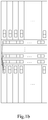
- the implementation mode of the latest high-capacity backboard is a design of a belt type, as shown in FIG. 1a and 1b .
- FIG. 1a and 1b show a device structure with three layers at one side.
- the capacity of six layers at double sides is double, and the structure of the other side is basically as same as that in the FIG. 1 .
- M switch cards are inserted laterally in the middle, and single boards vertically inserted on the upper and lower layers are N line cards.
- the line cards on the lower layer are forward inserted cards, and the single boards on the lower layer are backward inserted cards.
- High-speed socket positions are shown in small boxes of FIG. 1b .
- distances between line card sockets and switch card sockets are kept as close as possible, to ensure the performance of the high-speed signals. That design can guarantee reliable transmission of 12.5G high-speed signals of the backboard.
- about 25T of the total capacity of the device is achieved.
- the bandwidth and capacity unit of the device is Gbps (10 to the 9 bit per second) or Tbps (10 to the 12 bit per second), which represents the amount of data able to be transmitted or switched by the device per second, usually abbreviated as G or T.
- US 8218537 B1 discloses a serial channel switch circuit and modular packet switch using the serial channel switch circuits.
- US2003142483 A1 discloses a switching device comprising at least one line card and at least one switching card, as well as a mid-plane coupled to the at least one line card and the at least one switching card, wherein the at least one switching card and the at least one line card are perpendicular to each other, such that the interconnections are short and can be implemented in a few layers.
- the present invention provides a backboard structure and centralized switching device according to appended independent claims, to solve at least the above technical problems. Further improvements and embodiments are provided in the dependent claims.
- the backboard structure includes a backboard, and further includes: a line card, arranged at a front side of the backboard; and a switch card, arranged at a back side of the backboard.
- the backboard structure further includes: a first socket for connecting the line card to the switch card, arranged at the front side of the backboard; a second socket for connecting the switch card to the line card, arranged at the back side of the backboard.
- the first socket and the second socket are orthogonally arranged on a same layer.
- the first socket is directly connected with the second socket through the backboard.
- the backboard structure further includes: the third socket, arranged on the backboard, and connected with the first socket; a fourth socket connected with the third socket, arranged on the backboard, and connected to the switch card.
- the first socket is connected with the second socket through the third socket and the fourth socket.
- the backboard structure further includes: a cable box, arranged on the backboard, for cross-layer connecting the switch card and the line card.
- the backboard structure further includes: a fifth socket for connecting the line card to the cable box, and a sixth socket for connecting the cable box to the line card; a seventh socket for connecting the switch card to the cable box, and an eighth socket for connecting the cable box to the switch card.
- the fifth socket is directly connected with the sixth socket across the backboard; or, the fifth socket is indirectly connected with the sixth socket through a ninth socket arranged on the backboard.
- the sixth socket is arranged adjacent to a panel of the switch card.
- the second socket and the sixth socket are respectively arranged at both sides of a switch chip on the switch card.
- the cable box and the switch card are arranged at a same side of the backboard.
- the cable box and the switch card are arranged in parallel.
- a centralized switching device including a switch card and a line card, and further including the above backboard structure.
- the present invention adopts the technical means of arranging the first socket for connecting the line card to the switch card and the second socket for connecting the switch card to the line card respectively at two sides of the backboard, to solve the problems of poor transmission performance of a backboard solution and small design space of a single board in the related art. Therefore, the requirement for path loss of high-speed signals is met, and the design space of the single board is increased at the same time.
- the line card in the present embodiment may be called service board, line board, customer board, branch board, etc., in various devices, and is a PCB board card which supports the external service access and communicates with the switch board card through the socket of the backboard.
- the switch card may be called switch board, switch board card, cross board, etc., in various devices, which is a PCB board card for connecting the switch or cross scheduling function among various line cards.
- the cable backboard (referred to as the backboard for short) is a backboard concept in a board sense, including backboard PCB.
- a cable box for implementing the high-speed interconnection between the line card and the switch card in the following embodiments (including socket and high speed cable) is arranged on the backboard.
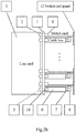
- a backboard structure as shown in FIG. 3a and 3b , includes: a backboard 1, a first socket 2 for connecting the line card to the switch card, arranged at the front side of the backboard 1; a second socket 9 for connecting the switch card to the line card, arranged at the back side of the backboard 1.
- the first socket 2 and the second socket 9 are orthogonally arranged on the same layer.
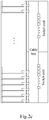
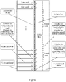
- the line card and the switch card are arranged at different sides of the backboard, that is, the line card is arranged at the front side of the back plane, and the switch card is arranged at the back side of the backboard (as shown in FIG. 2a , 2b and 2c ).
- the line card in the present embodiment includes a line card PCB 4 and a line card panel 5
- the switch card in the present embodiment includes a switch card PCB 11 and a switch card panel 12.
- the first socket 2 and the second socket 9 are connected directly through the backboard 1.
- the third socket 13 (not shown in the figure) is arranged on the backboard 1 and is connected with the first socket 2.
- the fourth socket 14 connected with the third socket 14 (not shown in the figure) is arranged on the backboard 1 and is connected with the switch card.
- the first socket 2 is connected with the second socket 9 through the third socket 13 and the fourth socket 14.
- the backboard structure provided by the present embodiment may also include: a cable box 6, arranged on the backboard 1, for cross-layer connecting the switch card and the line card.
- the above backboard structure may also include: a fifth socket 3 for connecting the line card to the cable box 6, and a sixth socket 10 for connecting the cable box 6 to the line card; a seventh socket 8 for connecting the switch card to the cable box 6, and an eighth socket 7 for connecting the cable box 6 to the switch card.
- the fifth socket 3 and the sixth socket 10 are connected directly through the backboard 1. Or, the fifth socket 3 and the sixth socket 10 are indirectly connected through a ninth socket (not shown in the figure) arranged on the backboard 1.
- the sixth socket 10 is arranged adjacent to the panel 12 of the switch card.
- the second socket 9 and the sixth socket 10 are respectively arranged at both sides of the switch chip on the switch card, to ensure that the distance from the switch chip to the second socket 9 is equal to the distance from the switch chip to with the sixth socket 10.
- the cable box 6 and the switch card are arranged at the same side of the backboard 1.
- the cable box 6 and the switch card are arranged in parallel.
- the present embodiment also provides a centralized switching device, including a switch card, a line card and the above-mentioned backboard structure.
- the switch card is arranged at the back side of the backboard structure, and the line card is arranged at the front side of the backboard.
- the present embodiment provides a backboard interconnection structure realized by using a cable, which can be used in a communication device adopting a centralized switching or branch structure, such as, optical transmission network (referred to as OTN for short), or packet transfer network (referred to as PTN for short), or router or the like.
- OTN optical transmission network
- PTN packet transfer network
- the centralized switching device usually includes a plurality of line cards and a plurality of switch board cards. Every line card and every switch board card must have enough physical connection paths; and the high speed cables are used to implement the physical path connection, which is a new backboard technology.
- the new backboard technology can reduce the transmission loss, improve the connection distance, and thus improve the number of line cards and the maximum switching capacity of the device.
- One of the basic functions required to be implemented by the backboard of the centralized switch device is to ensure that at least one connection path among all line cards and all switch cards; in that way, the data scheduling among any line cards can be implemented.
- the present embodiment further reduces the loss of the high-speed signal, increases the usable space of the line card, and provides greater device capacity which is larger than 50T and lager single slot line card access bandwidth 800G/1T.
- the device shapes in the present embodiment are as shown in FIG. 2a , FIG. 2b , FIG. 2c , FIG. 3a and 3b , and in FIG. 4 .
- the device based on the cable backboard of the present invention is composed of the following components:
- the components 2, 3, 4 and 5 constitute the line card unit.
- the components 1, 13, 14 and 15 constitute the backboard PCB unit.
- the components 6, 7 and 10 constitute the cable box unit.
- the components 8, 9, 11 and 12 constitute the switch card unit.
- the backboard PCB unit and the cable box unit can be collectively referred to as a cable backboard.
- every line card is provided with y backboard sockets (components 2), and every switch card is provided with N/c backboard sockets (components 9), and the components 2 and 9 may select the orthogonal socket for direct mutual inserting, and may also be interconnected through the transfer of the components 13 and 14.
- the data connection cross the device layers are implemented through the cable box.
- the cable box is also installed at the back side of the device, and is arranged in parallel with the switch card, and is longitudinal cross the position of all switch cards in one column.
- the sockets (components 10) at one side of the cable box are connected with all line card sockets (components 3), and the sockets (components 7) at another side are connected with the switch card sockets (components 8) in a corresponding column.
- the cable box is a pre-installed component, and the cable box is fixed on the device frame through a structural element before the device leaves factory.
- the line cards and the switch cards may be inserted into the corresponding slots of the device after leaving factory.
- the position of the component 8 is at the PCB side of the switch card without the switch clip, and the components 8 and the component 9 are respectively arranged at both sides of the switch chip, to ensure that the PCB wiring of the switch chip to the component 8 and the component 9 is as short as possible.
- the number of the sockets (components 10) connected with the line cards at the left side of the cable box is N, that is, every line card slot has one; the number of the sockets (components 7) connected with the switch cards at the right side is Q, which can be determined according to the socket type selection, while as long as that the numbers of the data paths of which the Q components 7 and the N components 10 for transmission are same.
- the cable box internally uses high speed cables to connect the components 7 and the components 10. Every component 10 is divided into (c-1) parts, and the (c-1) parts are respectively connected to the components 7 on non-same layers. In this way, the cable box can achieve the mutual connectivity among every line card and every switch card on all non-same layers.
- the transmission loss of the high speed cable is very small relative to the PCB wiring, so that the loss of the whole transmission path can be controlled very low, to ensure the transmission performance of the high speed signal.
- the depths of the PCBs of the two may be designed respectively.
- the design of the switch board is relatively fixed, and the switch chip is the key, therefore, the depth of the switch card may be compressed as much as possible.
- the cable box and the switch card are arranged in parallel, and do not occupy additional device depth.
- new function board card will be developed continuously, so the requirement for the PCB space is relatively large.
- the embodiments of the present invention can solve the problem of increasing the PCB space of the line card well.
- the embodiment implements a design of 64-slot line cards and a single line card with an 800G bandwidth.
- the maximum capacity of the system is 51.2T.
- a structure of a double-layer switch card is adopted.
- a single line card has an 800G bandwidth, and a single physical connection rate is selected as 25G.
- the single line card needs 48 channels to transmit data, and considering protection, 64 physical channels are needed in total.
- the number of the switch cards may be selected as 8 and a 6+2 protection mode is adopted according to structure limitation.
- the 64 channels of the line card are allocated to 8 switch cards, and each switch card has 8 channels.
- the interconnection sockets (components 3 and 10) of the cable box and the line card select 4x4pair, and support 8 channels.
- the interconnection sockets (components 2 and 9) of the line card and the switch card select 4x4pair, and support 8 channels.
- the interconnection sockets (components 7 and 8) of the cable box and the switch card select 4x8pair, and support 16 channels.
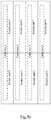
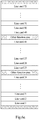
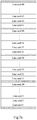
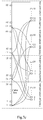
- a pattern of the embodiment is as shown in FIGS. 5a , 5b and 5c .
- the basic parameters are as follows.
- the embodiment implements a design of 72-slot line cards and a single line card with a 1T bandwidth.
- the maximum capacity of the system is 72T.
- a structure of a three-layer switch card is adopted.
- a single line card has a 1T bandwidth, and a single physical connection rate is selected as 25G.
- the single line card needs 60 channels to transmit data, and considering protection, 72 physical channels are needed in total.
- the number of the switch cards may be selected as 12 and a 10+2 protection mode is adopted according to structure limitation.
- the 72 channels of the line card are allocated to 12 switch cards, and each switch card has 8 channels.
- the interconnection sockets (components 3 and 10) of the cable box and the line card select 4x8pair, and support 16 channels.
- the interconnection sockets (components 2 and 9) of the line card and the switch card select 4x4pair, and support 8 channels.
- the basic parameters are as follows.
- the embodiment implements a design of 80-slot line card and a single line card with a 1T bandwidth.
- the maximum capacity of the system is 80T.
- a structure of a four-layer switch card is adopted.
- a single line card has a 1T bandwidth, and a single physical connection rate is selected as 25G.
- the single line card needs 60 channels to transmit data, and considering protection, 72 physical channels are needed in total.
- the number of the switch cards may be selected as 12 and a 10+2 protection mode is adopted according to structure limitation.
- the 72 channels of the line card are allocated to 12 switch cards, and each switch card has 8 channels.
- the interconnection sockets (components 3 and 10) of the cable box and the line card select 6x8pair, and support 24 channels.
- the interconnection sockets (components 2 and 9) of the line card and the switch card select 4x4pair, and support 8 channels.
- the basic parameters are as follows.
- the beneficial effects of the present embodiment are as follows:
- the connection paths of every line card and every cross board are made as short as possible, which can fully meet the requirement for the path loss of the 25G/28G high speed signal.
- the PCB design space of the line card is increased as much as possible, to meet the requirement for the big capacity design of the single card.
- the scheduling capacity of the whole device can be improved, and the system capacity over 100T can be realized.
Landscapes
- Engineering & Computer Science (AREA)
- Theoretical Computer Science (AREA)
- Signal Processing (AREA)
- Computer Networks & Wireless Communication (AREA)
- Human Computer Interaction (AREA)
- General Engineering & Computer Science (AREA)
- General Physics & Mathematics (AREA)
- Physics & Mathematics (AREA)
- Power Engineering (AREA)
- Computer Hardware Design (AREA)
- Microelectronics & Electronic Packaging (AREA)
- Use Of Switch Circuits For Exchanges And Methods Of Control Of Multiplex Exchanges (AREA)
- Data Exchanges In Wide-Area Networks (AREA)
- Structure Of Telephone Exchanges (AREA)
Claims (10)
- Rückbrettstruktur, umfassend: ein Rückbrett;
eine Line-Karte, die an einer Vorderfläche des Rückbretts angeordnet ist;
eine Switch-Karte, die an einer Rückfläche des Rückbretts angeordnet ist;
einen ersten Anschluss zum Verbinden der Line-Karte mit der Switch-Karte, angeordnet an der Vorderseite des Rückbretts;
einen zweiten Anschluss zum Verbinden der Switch-Karte mit der Line-Karte, angeordnet an der Rückseite des Rückbretts;
wobei der erste Anschluss und der zweite Anschluss orthogonal an einer gleichen Schicht angeordnet sind;
dadurch gekennzeichnet, dass die Rückbrettstruktur ferner Folgendes umfasst:
eine Kabelbox, angeordnet an dem Rückbrett, zum querschichtverbinden der Switch-Karte und der Line-Karte. - Rückbrettstruktur nach Anspruch 1, wobei
der erste Anschluss durch das Rückbrett direkt mit dem zweiten Anschluss verbunden ist. - Rückbrettstruktur nach Anspruch 1, wobei die Rückbrettstruktur ferner Folgendes umfasst:den dritten Anschluss, der an dem Rückbrett angeordnet ist und mit dem ersten Anschluss verbunden ist;einen mit dritten Anschluss verbundenen vierten Anschluss, der an dem Rückbrett angeordnet ist und mit der Switch-Karte verbunden ist; undden ersten Anschluss, der mit dem zweiten Anschluss durch den dritten Anschluss und den vierten Anschluss verbunden ist.
- Rückbrettstruktur nach Anspruch 1, wobei die Rückbrettstruktur ferner Folgendes umfasst:einen fünften Anschluss zum Verbinden der Line-Karte mit der Kabelbox, und einen sechsten Anschluss zum Verbinden der Kabelbox mit der Line-Karte; undeinen siebten Anschluss zum Verbinden der Switch-Karte mit der Kabelbox, und einen achten Anschluss zum Verbinden der Kabelbox mit der Switch-Karte.
- Rückbrettstruktur nach Anspruch 4, wobei
der fünfte Anschluss direkt mit dem sechsten Anschluss durch das Rückbrett verbunden ist; oder der fünfte Anschluss indirekt mit dem sechsten Anschluss durch einen neunten Anschluss, angeordnet an dem Rückbrett, verbunden ist. - Rückbrettstruktur nach Anspruch 5, wobei der sechste Anschluss neben einer Wand der Switch-Karte angeordnet ist.
- Rückbrettstruktur nach Anspruch 4, wobei der zweite Anschluss und der sechste Anschluss jeweils an beiden Seiten eines Switchchips an der Switch-Karte angeordnet sind.
- Rückbrettstruktur nach Anspruch 1, wobei die Kabelbox und die Switch-Karte an einer gleichen Seite des Rückbretts angeordnet sind.
- Rückbrettstruktur nach Anspruch 8, wobei die Kabelbox und die Switch-Karte parallel angeordnet sind.
- Zentralisierte Schaltvorrichtung, umfassend eine Switch-Karte und eine Line-Karte und ferner Folgendes umfassend: eine Rückbrettstruktur wie beschrieben nach einem der Ansprüche 1-9.
Applications Claiming Priority (2)
| Application Number | Priority Date | Filing Date | Title |
|---|---|---|---|
| CN201410348765.4A CN105281917A (zh) | 2014-07-21 | 2014-07-21 | 背板结构及集中交换设备 |
| PCT/CN2014/094559 WO2015117519A1 (zh) | 2014-07-21 | 2014-12-22 | 背板结构及集中交换设备 |
Publications (3)
| Publication Number | Publication Date |
|---|---|
| EP3197112A1 EP3197112A1 (de) | 2017-07-26 |
| EP3197112A4 EP3197112A4 (de) | 2017-09-06 |
| EP3197112B1 true EP3197112B1 (de) | 2019-09-18 |
Family
ID=53777322
Family Applications (1)
| Application Number | Title | Priority Date | Filing Date |
|---|---|---|---|
| EP14881449.4A Active EP3197112B1 (de) | 2014-07-21 | 2014-12-22 | Rückwandstruktur und zentralisierte schaltvorrichtung |
Country Status (5)
| Country | Link |
|---|---|
| EP (1) | EP3197112B1 (de) |
| JP (1) | JP2017521960A (de) |
| KR (1) | KR20170034413A (de) |
| CN (1) | CN105281917A (de) |
| WO (1) | WO2015117519A1 (de) |
Cited By (1)
| Publication number | Priority date | Publication date | Assignee | Title |
|---|---|---|---|---|
| US11196196B2 (en) | 2017-06-09 | 2021-12-07 | Huawei Technologies Co., Ltd. | Connection apparatus, network board connection system, and communications device |
Families Citing this family (8)
| Publication number | Priority date | Publication date | Assignee | Title |
|---|---|---|---|---|
| CN108011214B (zh) | 2016-10-31 | 2020-09-08 | 新华三技术有限公司 | 线缆背板系统及通信设备 |
| CN108879150B (zh) * | 2017-05-15 | 2020-12-15 | 华为技术有限公司 | 一种线缆背板以及通讯设备 |
| CN109757052B (zh) * | 2017-11-06 | 2021-11-02 | 中兴通讯股份有限公司 | 一种通信设备数据信号传输装置及通信设备 |
| CN108183872B (zh) * | 2017-12-27 | 2020-12-22 | 中科曙光信息产业成都有限公司 | 交换机系统及其构建方法 |
| CN108134750B (zh) * | 2017-12-27 | 2021-06-29 | 迈普通信技术股份有限公司 | 一种背板及通信设备 |
| CN109996414A (zh) * | 2017-12-29 | 2019-07-09 | 中兴通讯股份有限公司 | 一种线缆背板、线缆盒和线缆组件 |
| CN111381640B (zh) * | 2020-03-16 | 2021-06-18 | 黄河水利职业技术学院 | 一种计算机主机箱用多功能理线器 |
| CN115714930A (zh) * | 2022-09-30 | 2023-02-24 | 超聚变数字技术有限公司 | 数据转发设备、计算设备及机柜 |
Citations (1)
| Publication number | Priority date | Publication date | Assignee | Title |
|---|---|---|---|---|
| US20030142483A1 (en) * | 2002-01-30 | 2003-07-31 | Ofer Iny | Switching device and a method for the configuration thereof |
Family Cites Families (8)
| Publication number | Priority date | Publication date | Assignee | Title |
|---|---|---|---|---|
| JPS581445B2 (ja) * | 1975-08-13 | 1983-01-11 | 富士通株式会社 | カイロトウサイヨウカ−ドジツソウホウ |
| US7009939B2 (en) * | 2001-05-21 | 2006-03-07 | Lucent Technologies Inc. | Adaptive resource management in a communication system |
| CN100384169C (zh) * | 2005-10-19 | 2008-04-23 | 华为技术有限公司 | 接入设备中的主从框级联系统 |
| CN101242281B (zh) * | 2007-02-07 | 2010-08-18 | 华为技术有限公司 | 一种椅子背结构的数字用户线路接入系统 |
| US8848722B2 (en) * | 2007-03-14 | 2014-09-30 | Zonit Structured Solutions, Llc | Data center network distribution system |
| US8233477B1 (en) * | 2008-03-24 | 2012-07-31 | Force10 Networks, Inc. | Dynamic crosstalk reduction for backplane serial channels |
| CN102809784B (zh) * | 2011-06-02 | 2014-08-27 | 富士康(昆山)电脑接插件有限公司 | 光背板组件 |
| US8767725B2 (en) * | 2012-04-20 | 2014-07-01 | Hewlett-Packard Development Company, L.P. | Backplane module |
-
2014
- 2014-07-21 CN CN201410348765.4A patent/CN105281917A/zh active Pending
- 2014-12-22 KR KR1020177004811A patent/KR20170034413A/ko not_active Ceased
- 2014-12-22 EP EP14881449.4A patent/EP3197112B1/de active Active
- 2014-12-22 JP JP2017503094A patent/JP2017521960A/ja active Pending
- 2014-12-22 WO PCT/CN2014/094559 patent/WO2015117519A1/zh not_active Ceased
Patent Citations (1)
| Publication number | Priority date | Publication date | Assignee | Title |
|---|---|---|---|---|
| US20030142483A1 (en) * | 2002-01-30 | 2003-07-31 | Ofer Iny | Switching device and a method for the configuration thereof |
Cited By (1)
| Publication number | Priority date | Publication date | Assignee | Title |
|---|---|---|---|---|
| US11196196B2 (en) | 2017-06-09 | 2021-12-07 | Huawei Technologies Co., Ltd. | Connection apparatus, network board connection system, and communications device |
Also Published As
| Publication number | Publication date |
|---|---|
| JP2017521960A (ja) | 2017-08-03 |
| EP3197112A4 (de) | 2017-09-06 |
| WO2015117519A1 (zh) | 2015-08-13 |
| EP3197112A1 (de) | 2017-07-26 |
| KR20170034413A (ko) | 2017-03-28 |
| CN105281917A (zh) | 2016-01-27 |
Similar Documents
| Publication | Publication Date | Title |
|---|---|---|
| EP3197112A1 (de) | Rückwandstruktur und zentralisierte schaltvorrichtung | |
| US11038313B1 (en) | Orthogonal cross-connecting of printed circuit boards without a midplane board | |
| US10084255B2 (en) | Perpendicular and orthogonal interconnection system and communications device | |
| CN106954102B (zh) | 一种光背板子架装置 | |
| CN100561925C (zh) | 一种提高交换带宽的交换系统及方法 | |
| TWI668557B (zh) | 伺服器系統 | |
| CN102307142A (zh) | 背板系统 | |
| WO2014146231A1 (zh) | 背板、插框和网络设备 | |
| CN105376659B (zh) | 一种光背板组件及一种通信设备 | |
| US10476816B2 (en) | Lite network switch architecture | |
| JP6966649B2 (ja) | ケーブルバックボード、ケーブルボックスおよびケーブルアセンブリ | |
| CN102497308B (zh) | 一种多槽位交换机 | |
| US9603275B2 (en) | Blackplane board and wiring method of backplane board | |
| EP3068088A1 (de) | Verbindungssystem für kommunikationsvorrichtung | |
| US9750135B2 (en) | Dual faced ATCA backplane | |
| CN108134750B (zh) | 一种背板及通信设备 | |
| EP2897325B1 (de) | Kommunikationssystem | |
| CN117156774A (zh) | 一种机柜服务器 | |
| CN105591950B (zh) | 一种网络设备及其组件 | |
| CN103455104A (zh) | 一种交换板及刀片服务器 | |
| JP2017118187A (ja) | 中継装置、ラインカード | |
| KR100450403B1 (ko) | 스위치가 사용되는 시스템의 고속 백플레인 | |
| KR20170093596A (ko) | 미드플레인 통신 시스템 | |
| WO2016177133A1 (zh) | 业务板及具有其的通信设备 |
Legal Events
| Date | Code | Title | Description |
|---|---|---|---|
| STAA | Information on the status of an ep patent application or granted ep patent |
Free format text: STATUS: THE INTERNATIONAL PUBLICATION HAS BEEN MADE |
|
| PUAI | Public reference made under article 153(3) epc to a published international application that has entered the european phase |
Free format text: ORIGINAL CODE: 0009012 |
|
| STAA | Information on the status of an ep patent application or granted ep patent |
Free format text: STATUS: REQUEST FOR EXAMINATION WAS MADE |
|
| 17P | Request for examination filed |
Effective date: 20170220 |
|
| AK | Designated contracting states |
Kind code of ref document: A1 Designated state(s): AL AT BE BG CH CY CZ DE DK EE ES FI FR GB GR HR HU IE IS IT LI LT LU LV MC MK MT NL NO PL PT RO RS SE SI SK SM TR |
|
| AX | Request for extension of the european patent |
Extension state: BA ME |
|
| A4 | Supplementary search report drawn up and despatched |
Effective date: 20170807 |
|
| RIC1 | Information provided on ipc code assigned before grant |
Ipc: H04L 12/931 20130101AFI20170801BHEP |
|
| DAX | Request for extension of the european patent (deleted) | ||
| GRAP | Despatch of communication of intention to grant a patent |
Free format text: ORIGINAL CODE: EPIDOSNIGR1 |
|
| STAA | Information on the status of an ep patent application or granted ep patent |
Free format text: STATUS: GRANT OF PATENT IS INTENDED |
|
| RIC1 | Information provided on ipc code assigned before grant |
Ipc: H05K 7/14 20060101ALI20190322BHEP Ipc: H04L 12/931 20130101AFI20190322BHEP Ipc: G06F 1/18 20060101ALI20190322BHEP |
|
| INTG | Intention to grant announced |
Effective date: 20190412 |
|
| GRAS | Grant fee paid |
Free format text: ORIGINAL CODE: EPIDOSNIGR3 |
|
| GRAA | (expected) grant |
Free format text: ORIGINAL CODE: 0009210 |
|
| STAA | Information on the status of an ep patent application or granted ep patent |
Free format text: STATUS: THE PATENT HAS BEEN GRANTED |
|
| AK | Designated contracting states |
Kind code of ref document: B1 Designated state(s): AL AT BE BG CH CY CZ DE DK EE ES FI FR GB GR HR HU IE IS IT LI LT LU LV MC MK MT NL NO PL PT RO RS SE SI SK SM TR |
|
| REG | Reference to a national code |
Ref country code: GB Ref legal event code: FG4D |
|
| REG | Reference to a national code |
Ref country code: CH Ref legal event code: EP |
|
| REG | Reference to a national code |
Ref country code: DE Ref legal event code: R096 Ref document number: 602014054060 Country of ref document: DE |
|
| REG | Reference to a national code |
Ref country code: AT Ref legal event code: REF Ref document number: 1182631 Country of ref document: AT Kind code of ref document: T Effective date: 20191015 |
|
| REG | Reference to a national code |
Ref country code: IE Ref legal event code: FG4D |
|
| REG | Reference to a national code |
Ref country code: NL Ref legal event code: MP Effective date: 20190918 |
|
| PG25 | Lapsed in a contracting state [announced via postgrant information from national office to epo] |
Ref country code: HR Free format text: LAPSE BECAUSE OF FAILURE TO SUBMIT A TRANSLATION OF THE DESCRIPTION OR TO PAY THE FEE WITHIN THE PRESCRIBED TIME-LIMIT Effective date: 20190918 Ref country code: LT Free format text: LAPSE BECAUSE OF FAILURE TO SUBMIT A TRANSLATION OF THE DESCRIPTION OR TO PAY THE FEE WITHIN THE PRESCRIBED TIME-LIMIT Effective date: 20190918 Ref country code: NO Free format text: LAPSE BECAUSE OF FAILURE TO SUBMIT A TRANSLATION OF THE DESCRIPTION OR TO PAY THE FEE WITHIN THE PRESCRIBED TIME-LIMIT Effective date: 20191218 Ref country code: BG Free format text: LAPSE BECAUSE OF FAILURE TO SUBMIT A TRANSLATION OF THE DESCRIPTION OR TO PAY THE FEE WITHIN THE PRESCRIBED TIME-LIMIT Effective date: 20191218 Ref country code: FI Free format text: LAPSE BECAUSE OF FAILURE TO SUBMIT A TRANSLATION OF THE DESCRIPTION OR TO PAY THE FEE WITHIN THE PRESCRIBED TIME-LIMIT Effective date: 20190918 Ref country code: SE Free format text: LAPSE BECAUSE OF FAILURE TO SUBMIT A TRANSLATION OF THE DESCRIPTION OR TO PAY THE FEE WITHIN THE PRESCRIBED TIME-LIMIT Effective date: 20190918 |
|
| REG | Reference to a national code |
Ref country code: LT Ref legal event code: MG4D |
|
| PG25 | Lapsed in a contracting state [announced via postgrant information from national office to epo] |
Ref country code: RS Free format text: LAPSE BECAUSE OF FAILURE TO SUBMIT A TRANSLATION OF THE DESCRIPTION OR TO PAY THE FEE WITHIN THE PRESCRIBED TIME-LIMIT Effective date: 20190918 Ref country code: LV Free format text: LAPSE BECAUSE OF FAILURE TO SUBMIT A TRANSLATION OF THE DESCRIPTION OR TO PAY THE FEE WITHIN THE PRESCRIBED TIME-LIMIT Effective date: 20190918 Ref country code: GR Free format text: LAPSE BECAUSE OF FAILURE TO SUBMIT A TRANSLATION OF THE DESCRIPTION OR TO PAY THE FEE WITHIN THE PRESCRIBED TIME-LIMIT Effective date: 20191219 Ref country code: AL Free format text: LAPSE BECAUSE OF FAILURE TO SUBMIT A TRANSLATION OF THE DESCRIPTION OR TO PAY THE FEE WITHIN THE PRESCRIBED TIME-LIMIT Effective date: 20190918 |
|
| REG | Reference to a national code |
Ref country code: AT Ref legal event code: MK05 Ref document number: 1182631 Country of ref document: AT Kind code of ref document: T Effective date: 20190918 |
|
| PG25 | Lapsed in a contracting state [announced via postgrant information from national office to epo] |
Ref country code: NL Free format text: LAPSE BECAUSE OF FAILURE TO SUBMIT A TRANSLATION OF THE DESCRIPTION OR TO PAY THE FEE WITHIN THE PRESCRIBED TIME-LIMIT Effective date: 20190918 Ref country code: AT Free format text: LAPSE BECAUSE OF FAILURE TO SUBMIT A TRANSLATION OF THE DESCRIPTION OR TO PAY THE FEE WITHIN THE PRESCRIBED TIME-LIMIT Effective date: 20190918 Ref country code: EE Free format text: LAPSE BECAUSE OF FAILURE TO SUBMIT A TRANSLATION OF THE DESCRIPTION OR TO PAY THE FEE WITHIN THE PRESCRIBED TIME-LIMIT Effective date: 20190918 Ref country code: PT Free format text: LAPSE BECAUSE OF FAILURE TO SUBMIT A TRANSLATION OF THE DESCRIPTION OR TO PAY THE FEE WITHIN THE PRESCRIBED TIME-LIMIT Effective date: 20200120 Ref country code: RO Free format text: LAPSE BECAUSE OF FAILURE TO SUBMIT A TRANSLATION OF THE DESCRIPTION OR TO PAY THE FEE WITHIN THE PRESCRIBED TIME-LIMIT Effective date: 20190918 Ref country code: IT Free format text: LAPSE BECAUSE OF FAILURE TO SUBMIT A TRANSLATION OF THE DESCRIPTION OR TO PAY THE FEE WITHIN THE PRESCRIBED TIME-LIMIT Effective date: 20190918 Ref country code: PL Free format text: LAPSE BECAUSE OF FAILURE TO SUBMIT A TRANSLATION OF THE DESCRIPTION OR TO PAY THE FEE WITHIN THE PRESCRIBED TIME-LIMIT Effective date: 20190918 Ref country code: ES Free format text: LAPSE BECAUSE OF FAILURE TO SUBMIT A TRANSLATION OF THE DESCRIPTION OR TO PAY THE FEE WITHIN THE PRESCRIBED TIME-LIMIT Effective date: 20190918 |
|
| PG25 | Lapsed in a contracting state [announced via postgrant information from national office to epo] |
Ref country code: IS Free format text: LAPSE BECAUSE OF FAILURE TO SUBMIT A TRANSLATION OF THE DESCRIPTION OR TO PAY THE FEE WITHIN THE PRESCRIBED TIME-LIMIT Effective date: 20200224 Ref country code: SK Free format text: LAPSE BECAUSE OF FAILURE TO SUBMIT A TRANSLATION OF THE DESCRIPTION OR TO PAY THE FEE WITHIN THE PRESCRIBED TIME-LIMIT Effective date: 20190918 Ref country code: CZ Free format text: LAPSE BECAUSE OF FAILURE TO SUBMIT A TRANSLATION OF THE DESCRIPTION OR TO PAY THE FEE WITHIN THE PRESCRIBED TIME-LIMIT Effective date: 20190918 Ref country code: SM Free format text: LAPSE BECAUSE OF FAILURE TO SUBMIT A TRANSLATION OF THE DESCRIPTION OR TO PAY THE FEE WITHIN THE PRESCRIBED TIME-LIMIT Effective date: 20190918 |
|
| REG | Reference to a national code |
Ref country code: DE Ref legal event code: R097 Ref document number: 602014054060 Country of ref document: DE |
|
| PLBE | No opposition filed within time limit |
Free format text: ORIGINAL CODE: 0009261 |
|
| STAA | Information on the status of an ep patent application or granted ep patent |
Free format text: STATUS: NO OPPOSITION FILED WITHIN TIME LIMIT |
|
| PG2D | Information on lapse in contracting state deleted |
Ref country code: IS |
|
| PG25 | Lapsed in a contracting state [announced via postgrant information from national office to epo] |
Ref country code: DK Free format text: LAPSE BECAUSE OF FAILURE TO SUBMIT A TRANSLATION OF THE DESCRIPTION OR TO PAY THE FEE WITHIN THE PRESCRIBED TIME-LIMIT Effective date: 20190918 Ref country code: IS Free format text: LAPSE BECAUSE OF FAILURE TO SUBMIT A TRANSLATION OF THE DESCRIPTION OR TO PAY THE FEE WITHIN THE PRESCRIBED TIME-LIMIT Effective date: 20200119 |
|
| REG | Reference to a national code |
Ref country code: CH Ref legal event code: PL |
|
| 26N | No opposition filed |
Effective date: 20200619 |
|
| REG | Reference to a national code |
Ref country code: BE Ref legal event code: MM Effective date: 20191231 |
|
| PG25 | Lapsed in a contracting state [announced via postgrant information from national office to epo] |
Ref country code: SI Free format text: LAPSE BECAUSE OF FAILURE TO SUBMIT A TRANSLATION OF THE DESCRIPTION OR TO PAY THE FEE WITHIN THE PRESCRIBED TIME-LIMIT Effective date: 20190918 Ref country code: MC Free format text: LAPSE BECAUSE OF FAILURE TO SUBMIT A TRANSLATION OF THE DESCRIPTION OR TO PAY THE FEE WITHIN THE PRESCRIBED TIME-LIMIT Effective date: 20190918 |
|
| GBPC | Gb: european patent ceased through non-payment of renewal fee |
Effective date: 20191222 |
|
| PG25 | Lapsed in a contracting state [announced via postgrant information from national office to epo] |
Ref country code: LU Free format text: LAPSE BECAUSE OF NON-PAYMENT OF DUE FEES Effective date: 20191222 Ref country code: FR Free format text: LAPSE BECAUSE OF NON-PAYMENT OF DUE FEES Effective date: 20191231 Ref country code: IE Free format text: LAPSE BECAUSE OF NON-PAYMENT OF DUE FEES Effective date: 20191222 Ref country code: GB Free format text: LAPSE BECAUSE OF NON-PAYMENT OF DUE FEES Effective date: 20191222 |
|
| PG25 | Lapsed in a contracting state [announced via postgrant information from national office to epo] |
Ref country code: BE Free format text: LAPSE BECAUSE OF NON-PAYMENT OF DUE FEES Effective date: 20191231 Ref country code: CH Free format text: LAPSE BECAUSE OF NON-PAYMENT OF DUE FEES Effective date: 20191231 Ref country code: LI Free format text: LAPSE BECAUSE OF NON-PAYMENT OF DUE FEES Effective date: 20191231 |
|
| PG25 | Lapsed in a contracting state [announced via postgrant information from national office to epo] |
Ref country code: CY Free format text: LAPSE BECAUSE OF FAILURE TO SUBMIT A TRANSLATION OF THE DESCRIPTION OR TO PAY THE FEE WITHIN THE PRESCRIBED TIME-LIMIT Effective date: 20190918 |
|
| PG25 | Lapsed in a contracting state [announced via postgrant information from national office to epo] |
Ref country code: HU Free format text: LAPSE BECAUSE OF FAILURE TO SUBMIT A TRANSLATION OF THE DESCRIPTION OR TO PAY THE FEE WITHIN THE PRESCRIBED TIME-LIMIT; INVALID AB INITIO Effective date: 20141222 Ref country code: MT Free format text: LAPSE BECAUSE OF FAILURE TO SUBMIT A TRANSLATION OF THE DESCRIPTION OR TO PAY THE FEE WITHIN THE PRESCRIBED TIME-LIMIT Effective date: 20190918 |
|
| REG | Reference to a national code |
Ref country code: DE Ref legal event code: R079 Ref document number: 602014054060 Country of ref document: DE Free format text: PREVIOUS MAIN CLASS: H04L0012931000 Ipc: H04L0049100000 |
|
| PG25 | Lapsed in a contracting state [announced via postgrant information from national office to epo] |
Ref country code: TR Free format text: LAPSE BECAUSE OF FAILURE TO SUBMIT A TRANSLATION OF THE DESCRIPTION OR TO PAY THE FEE WITHIN THE PRESCRIBED TIME-LIMIT Effective date: 20190918 |
|
| PG25 | Lapsed in a contracting state [announced via postgrant information from national office to epo] |
Ref country code: MK Free format text: LAPSE BECAUSE OF FAILURE TO SUBMIT A TRANSLATION OF THE DESCRIPTION OR TO PAY THE FEE WITHIN THE PRESCRIBED TIME-LIMIT Effective date: 20190918 |
|
| PGFP | Annual fee paid to national office [announced via postgrant information from national office to epo] |
Ref country code: DE Payment date: 20250930 Year of fee payment: 12 |