EP3182816B1 - Apparatus and method for inspection, and system and method for mounting components comprising same - Google Patents
Apparatus and method for inspection, and system and method for mounting components comprising same Download PDFInfo
- Publication number
- EP3182816B1 EP3182816B1 EP15831748.7A EP15831748A EP3182816B1 EP 3182816 B1 EP3182816 B1 EP 3182816B1 EP 15831748 A EP15831748 A EP 15831748A EP 3182816 B1 EP3182816 B1 EP 3182816B1
- Authority
- EP
- European Patent Office
- Prior art keywords
- information
- mounting
- equipment
- flexible array
- array board
- Prior art date
- Legal status (The legal status is an assumption and is not a legal conclusion. Google has not performed a legal analysis and makes no representation as to the accuracy of the status listed.)
- Active
Links
Images

Classifications
-
- H—ELECTRICITY
- H05—ELECTRIC TECHNIQUES NOT OTHERWISE PROVIDED FOR
- H05K—PRINTED CIRCUITS; CASINGS OR CONSTRUCTIONAL DETAILS OF ELECTRIC APPARATUS; MANUFACTURE OF ASSEMBLAGES OF ELECTRICAL COMPONENTS
- H05K13/00—Apparatus or processes specially adapted for manufacturing or adjusting assemblages of electric components
- H05K13/08—Monitoring manufacture of assemblages
-
- H—ELECTRICITY
- H05—ELECTRIC TECHNIQUES NOT OTHERWISE PROVIDED FOR
- H05K—PRINTED CIRCUITS; CASINGS OR CONSTRUCTIONAL DETAILS OF ELECTRIC APPARATUS; MANUFACTURE OF ASSEMBLAGES OF ELECTRICAL COMPONENTS
- H05K13/00—Apparatus or processes specially adapted for manufacturing or adjusting assemblages of electric components
- H05K13/04—Mounting of components, e.g. of leadless components
- H05K13/046—Surface mounting
- H05K13/0465—Surface mounting by soldering
-
- H—ELECTRICITY
- H05—ELECTRIC TECHNIQUES NOT OTHERWISE PROVIDED FOR
- H05K—PRINTED CIRCUITS; CASINGS OR CONSTRUCTIONAL DETAILS OF ELECTRIC APPARATUS; MANUFACTURE OF ASSEMBLAGES OF ELECTRICAL COMPONENTS
- H05K13/00—Apparatus or processes specially adapted for manufacturing or adjusting assemblages of electric components
- H05K13/08—Monitoring manufacture of assemblages
- H05K13/081—Integration of optical monitoring devices in assembly lines; Processes using optical monitoring devices specially adapted for controlling devices or machines in assembly lines
- H05K13/0815—Controlling of component placement on the substrate during or after manufacturing
-
- H—ELECTRICITY
- H05—ELECTRIC TECHNIQUES NOT OTHERWISE PROVIDED FOR
- H05K—PRINTED CIRCUITS; CASINGS OR CONSTRUCTIONAL DETAILS OF ELECTRIC APPARATUS; MANUFACTURE OF ASSEMBLAGES OF ELECTRICAL COMPONENTS
- H05K13/00—Apparatus or processes specially adapted for manufacturing or adjusting assemblages of electric components
- H05K13/08—Monitoring manufacture of assemblages
- H05K13/081—Integration of optical monitoring devices in assembly lines; Processes using optical monitoring devices specially adapted for controlling devices or machines in assembly lines
- H05K13/0817—Monitoring of soldering processes
-
- H—ELECTRICITY
- H05—ELECTRIC TECHNIQUES NOT OTHERWISE PROVIDED FOR
- H05K—PRINTED CIRCUITS; CASINGS OR CONSTRUCTIONAL DETAILS OF ELECTRIC APPARATUS; MANUFACTURE OF ASSEMBLAGES OF ELECTRICAL COMPONENTS
- H05K3/00—Apparatus or processes for manufacturing printed circuits
- H05K3/30—Assembling printed circuits with electric components, e.g. with resistors
- H05K3/303—Assembling printed circuits with electric components, e.g. with resistors with surface mounted components
-
- H—ELECTRICITY
- H05—ELECTRIC TECHNIQUES NOT OTHERWISE PROVIDED FOR
- H05K—PRINTED CIRCUITS; CASINGS OR CONSTRUCTIONAL DETAILS OF ELECTRIC APPARATUS; MANUFACTURE OF ASSEMBLAGES OF ELECTRICAL COMPONENTS
- H05K3/00—Apparatus or processes for manufacturing printed circuits
- H05K3/30—Assembling printed circuits with electric components, e.g. with resistors
- H05K3/32—Assembling printed circuits with electric components, e.g. with resistors electrically connecting electric components or wires to printed circuits
- H05K3/34—Assembling printed circuits with electric components, e.g. with resistors electrically connecting electric components or wires to printed circuits by soldering
- H05K3/3465—Application of solder
- H05K3/3485—Application of solder paste, slurry or powder
-
- H—ELECTRICITY
- H05—ELECTRIC TECHNIQUES NOT OTHERWISE PROVIDED FOR
- H05K—PRINTED CIRCUITS; CASINGS OR CONSTRUCTIONAL DETAILS OF ELECTRIC APPARATUS; MANUFACTURE OF ASSEMBLAGES OF ELECTRICAL COMPONENTS
- H05K1/00—Printed circuits
- H05K1/02—Details
- H05K1/0266—Marks, test patterns or identification means
- H05K1/0269—Marks, test patterns or identification means for visual or optical inspection
-
- H—ELECTRICITY
- H05—ELECTRIC TECHNIQUES NOT OTHERWISE PROVIDED FOR
- H05K—PRINTED CIRCUITS; CASINGS OR CONSTRUCTIONAL DETAILS OF ELECTRIC APPARATUS; MANUFACTURE OF ASSEMBLAGES OF ELECTRICAL COMPONENTS
- H05K1/00—Printed circuits
- H05K1/02—Details
- H05K1/03—Use of materials for the substrate
- H05K1/0393—Flexible materials
-
- H—ELECTRICITY
- H05—ELECTRIC TECHNIQUES NOT OTHERWISE PROVIDED FOR
- H05K—PRINTED CIRCUITS; CASINGS OR CONSTRUCTIONAL DETAILS OF ELECTRIC APPARATUS; MANUFACTURE OF ASSEMBLAGES OF ELECTRICAL COMPONENTS
- H05K2203/00—Indexing scheme relating to apparatus or processes for manufacturing printed circuits covered by H05K3/00
- H05K2203/01—Tools for processing; Objects used during processing
- H05K2203/0147—Carriers and holders
- H05K2203/0165—Holder for holding a Printed Circuit Board [PCB] during processing, e.g. during screen printing
-
- H—ELECTRICITY
- H05—ELECTRIC TECHNIQUES NOT OTHERWISE PROVIDED FOR
- H05K—PRINTED CIRCUITS; CASINGS OR CONSTRUCTIONAL DETAILS OF ELECTRIC APPARATUS; MANUFACTURE OF ASSEMBLAGES OF ELECTRICAL COMPONENTS
- H05K2203/00—Indexing scheme relating to apparatus or processes for manufacturing printed circuits covered by H05K3/00
- H05K2203/16—Inspection; Monitoring; Aligning
- H05K2203/163—Monitoring a manufacturing process
-
- H—ELECTRICITY
- H05—ELECTRIC TECHNIQUES NOT OTHERWISE PROVIDED FOR
- H05K—PRINTED CIRCUITS; CASINGS OR CONSTRUCTIONAL DETAILS OF ELECTRIC APPARATUS; MANUFACTURE OF ASSEMBLAGES OF ELECTRICAL COMPONENTS
- H05K2203/00—Indexing scheme relating to apparatus or processes for manufacturing printed circuits covered by H05K3/00
- H05K2203/16—Inspection; Monitoring; Aligning
- H05K2203/166—Alignment or registration; Control of registration
-
- H—ELECTRICITY
- H05—ELECTRIC TECHNIQUES NOT OTHERWISE PROVIDED FOR
- H05K—PRINTED CIRCUITS; CASINGS OR CONSTRUCTIONAL DETAILS OF ELECTRIC APPARATUS; MANUFACTURE OF ASSEMBLAGES OF ELECTRICAL COMPONENTS
- H05K3/00—Apparatus or processes for manufacturing printed circuits
- H05K3/0097—Processing two or more printed circuits simultaneously, e.g. made from a common substrate, or temporarily stacked circuit boards
-
- Y—GENERAL TAGGING OF NEW TECHNOLOGICAL DEVELOPMENTS; GENERAL TAGGING OF CROSS-SECTIONAL TECHNOLOGIES SPANNING OVER SEVERAL SECTIONS OF THE IPC; TECHNICAL SUBJECTS COVERED BY FORMER USPC CROSS-REFERENCE ART COLLECTIONS [XRACs] AND DIGESTS
- Y02—TECHNOLOGIES OR APPLICATIONS FOR MITIGATION OR ADAPTATION AGAINST CLIMATE CHANGE
- Y02P—CLIMATE CHANGE MITIGATION TECHNOLOGIES IN THE PRODUCTION OR PROCESSING OF GOODS
- Y02P70/00—Climate change mitigation technologies in the production process for final industrial or consumer products
- Y02P70/50—Manufacturing or production processes characterised by the final manufactured product
-
- Y—GENERAL TAGGING OF NEW TECHNOLOGICAL DEVELOPMENTS; GENERAL TAGGING OF CROSS-SECTIONAL TECHNOLOGIES SPANNING OVER SEVERAL SECTIONS OF THE IPC; TECHNICAL SUBJECTS COVERED BY FORMER USPC CROSS-REFERENCE ART COLLECTIONS [XRACs] AND DIGESTS
- Y10—TECHNICAL SUBJECTS COVERED BY FORMER USPC
- Y10T—TECHNICAL SUBJECTS COVERED BY FORMER US CLASSIFICATION
- Y10T29/00—Metal working
- Y10T29/49—Method of mechanical manufacture
- Y10T29/49002—Electrical device making
- Y10T29/49117—Conductor or circuit manufacturing
- Y10T29/49124—On flat or curved insulated base, e.g., printed circuit, etc.
- Y10T29/4913—Assembling to base an electrical component, e.g., capacitor, etc.
Definitions
- the present invention relates to an inspection apparatus and method, and further relates to a component mounting system including the same and a method thereof. More specifically, the present invention relates to an inspection apparatus and a method for a process of mounting components on a flexible array board, and a component mounting system including the same and a method thereof.
- the process of mounting electronic components on a printed circuit board proceeds in the order of: applying solder onto the pad of the printed circuit board through screen printer equipment; inspecting the solder application state through solder paste inspection (SPI) equipment; and mounting the electronic components through component mounting equipment by using a surface mount technology (SMT).
- SPI solder paste inspection
- SMT surface mount technology
- components may not be mounted in the correct positions of the flexible printed circuit board due to the characteristics of the flexible printed circuit board in which the flexible printed circuit board is thin and easily bent, thereby degrading the reliability of the component mounting process.
- WO2013/186963 and JP 2010 056143 are examples of inspection apparatuses.
- the present invention provides a solder paste inspection equipment according to claim 1 and a method to inspect a solder paste application according to claim 5. Further preferred embodiments are provided in the dependent claims.
- the mounting tolerance information of the component mounting equipment and the warp information of the flexible array board obtained through the inspection of the solder paste inspection equipment are comprehensively compared to set a mounting region for components, and the components are mounted only on the board or region where mounting of components is possible according thereto, thereby improving the efficiency and reliability of the component mounting process.
- first or second may be used to explain a variety of elements, but the elements are not limited to the terms. The terms are used only for the purpose of distinguishing one element from the other element.
- first element may be referred to as the second element, and likewise, the second element may be referred to as the first element without departing from the scope of the present invention.
- a combination of each block of the accompanying block diagrams and each step of the accompanying flowchart may be performed by computer program instructions.
- the computer program instructions may be installed in processors of general purpose computers, special purpose computers, or other programmable data processing equipment, and the instructions that are executed by the processors of the computers or other programmable data processing equipment create means for performing functions that are described in each block of the block diagram or in each step of the flowchart.
- the computer program instructions may be stored in a computer-available or computer-readable memory that is able to support the computers or other programmable data processing equipment in order to realize the function in a specific manner.
- the instructions stored in the computer-available or computer-readable memory may make manufactured articles that include instruction means for performing the function that is described in each block of the block diagrams or in each step of the flowchart. Since the computer program instructions can be installed in the computer or other programmable data processing equipment, the instructions that allow a series of operation steps to be performed in the computer or other programmable data processing equipment to create computer-executable processes to then operate the computer or the other programmable data processing equipment may provide steps for executing the functions that are described in each block of the block diagrams and in each step of the flowchart.
- each block or each step may represent a portion of a module, a segment, or code that includes one or more executable instructions for performing a specified logical function.
- each block or each step may occur out of the order. For example, two successive blocks or steps may be performed substantially at the same time, or, sometimes, may be performed in a reverse order depending upon the functions.
- FIG. 1 is a block diagram showing a component mounting system, according to an embodiment of the present invention.
- the component mounting system 100 is configured for mounting components on a flexible array board which is placed on a jig, and includes screen printer equipment 110, solder paste inspection equipment 120, and component mounting equipment 130.
- the component mounting system 100 may apply solder onto the flexible array board placed on the jig through the screen printer equipment 110, inspect the solder application state through the solder paste inspection equipment 120, and then mount components through the component mounting equipment 130.
- the flexible printed circuit board has characteristics of being easily bent or warped, mounting of components is performed in a state in which a plurality of boards is fixed to a jig in the form of an array for a component mounting process.
- the screen printer equipment 110 is configured for applying solder on a pad of the flexible array board, and may apply the solder on the pad of the flexible array board while a stencil mask that has an opening formed to correspond to the position of the pad is disposed on the flexible array board.
- the solder paste inspection equipment 120 inspects the solder application state through a measurement of the flexible array board which is transferred from the screen printer equipment 110. For example, the solder paste inspection equipment 120 obtains position information of the pad of the flexible array board and two-dimensional or three-dimensional shape information of the applied solder, and then inspects defects such as over-application, under-application, or inaccurate application of the solder by using the position and shape information.
- the component mounting equipment 130 mounts components on the flexible array board by referencing the inspection information of the solder paste inspection equipment 120. For example, when mounting the components on the flexible array board, the component mounting equipment 130 may align the components to the position of the pad by rotating a mounter head up to a predetermined angle to correspond to the rotational angle of the pad, and mount the components. However, since the rotational angle of the mounter head of the component mounting equipment 130 is determined to be within a predetermined range, it may be difficult to mount the components in a correct position when the flexible array board exceeds the maximum mounting angle of the component mounting equipment 130 due to a substantial warpage.
- the present embodiment may improve the efficiency and reliability of a component mounting process with respect to the flexible array board through interworking between the solder paste inspection equipment 120 and the component mounting equipment 130.
- FIG. 2 is a block diagram showing a structure of the solder paste inspection equipment, according to an embodiment of the present invention.
- the solder paste inspection equipment 120 may include an information transmitting/receiving unit 210, a measuring unit 220, and an analyzing unit 230.
- the information transmitting/receiving unit 210 may transmit and receive measurement and analysis information of the screen printer equipment 110 and the component mounting equipment 130 in a wired or wireless manner. In addition, the information transmitting/receiving unit 210 may also transmit the transmitted/received information to a predetermined computing device. For example, the information transmitting/receiving unit 210 may receive mounting tolerance information from the component mounting equipment 130, and thereafter, may transmit mount-impossible information to the component mounting equipment 130.
- the measuring unit 220 may measure the solder application state of the flexible array board in a two-dimensional or three-dimensional manner to obtain shape information of the solder, and may generate measurement information on the amount of rotation of the flexible array board and on the bending of the flexible array board.
- the analyzing unit 230 may derive an analyzed result based on the information measured by the measuring unit 220.
- the analyzing unit 230 may inspect defects, such as over-application, under-application, inaccurate application, the height, the warpage, etc. of the solder, through the shape information of the solder, and may set the region where the defects are detected as a first mount-impossible region based on the same.
- the analyzing unit 230 may generate warp information by using the measurement information on the amount of rotation of the flexible array board and on the bending of the flexible array board, and may set a second mount-impossible region based on the warp information and the mounting tolerance information of the component mounting equipment 130. That is, the mount-impossible region information may contain at least one of the first and the second mount-impossible region information, and may be information for determining whether or not mounting is possible by the component mounting equipment 130 prior to the mounting in order to prevent components from being mounted on the faulty region.
- the analyzing unit 230 may transmit the mount-impossible information to the information transmitting/receiving unit 210 for transmission to the component mounting equipment 130.
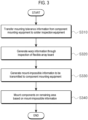
- FIG. 3 is a flowchart showing a component mounting method, according to an embodiment of the present invention.
- the mounting tolerance information may include maximum mounting angle information of the component mounting equipment 130. That is, the component mounting equipment 130 transmits, to the solder paste inspection equipment 120, information on maximum mounting angle, which represents the maximum angle to which the mounter head can rotate for mounting of components. Meanwhile, the mounting tolerance information may further include information such as a maximum mounting height of the mounter head, etc.
- the mounting tolerance information may be transmitted from the component mounting equipment 130 to the solder paste inspection equipment 120 according to a specified criterion of the component mounting system 100 (for example, at predetermined times or only at the time of initial setting).
- the solder paste inspection equipment 120 receives the mounting tolerance information from the component mounting equipment 130, and may separately generate warp information of the flexible array board through a measurement of the flexible array board that is placed on the jig (S320). For example, the solder paste inspection equipment 120 generates the warp information on the amount of rotation of the flexible array board and on the bending of the flexible array board by measuring at least one of a fiducial position, a pad position, or an outer line position of the flexible array board.
- two-dimensional information and three-dimensional information which may include the bending and curves of the board determined by using height information, may be used as the information on the amount of rotation and bending.
- the component mounting process is performed on a flexible array board while a plurality of flexible boards is placed on the jig in an array form.
- the solder paste inspection equipment 120 may generate warp information for each of the flexible array boards or warp information for each region thereof based on the fiducial information and the measurement information of the pads of the flexible array board.
- the solder paste inspection equipment 120 compares the mounting tolerance information transmitted from the component mounting equipment 130 with the warp information of the flexible array board generated by the solder paste inspection equipment 120 to generate mount-impossible information on a region where mounting of components is impossible, and transmits the mount-impossible information to the component mounting equipment 130 (S330). For example, if it is determined that the amount of rotation and the bending for each board or each region of the flexible array board exceeds the maximum mounting angle of the component mounting equipment 130 as a result of the measurement of the flexible array board, the solder paste inspection equipment 120 sets the corresponding board or region as a region where mounting of components is impossible and generates mount-impossible information (for example, pad information, coordinate information, or the like). The solder paste inspection equipment 120 transmits the generated mount-impossible information to the component mounting equipment 130.
- the component mounting equipment 130 mounts components on the remaining regions except for the mount-impossible region based on the mount-impossible information transmitted from the solder paste inspection equipment 120 (S340).
- the component mounting equipment 130 may not mount components on the boards that correspond to the mount-impossible information and may mount components on the remaining boards among the flexible array boards placed on the jig.
- the component mounting equipment 130 may not mount components on the region within a single board that corresponds to the mount-impossible information and may mount components on the remaining regions of the board.
- the mount-impossible information may include instruction information that instructs to exclude mounting of components on a corresponding board or a specific region in the corresponding board. Therefore, the component mounting equipment 130 that receives the corresponding instruction does not perform the mounting of components on the corresponding board or the specific region in the corresponding board.
- the mounting tolerance information of the component mounting equipment 130 and the warp information of the flexible array board obtained through the inspection of the solder paste inspection equipment 120 may be comprehensively compared to set a mounting region for components, and the components may be mounted only on the board or region where mounting of components is possible according thereto, thereby improving the efficiency and reliability of the component mounting process.
- component mounting system 110 screen printer equipment 120: solder paste inspection equipment 130: component mounting equipment
Landscapes
- Engineering & Computer Science (AREA)
- Manufacturing & Machinery (AREA)
- Microelectronics & Electronic Packaging (AREA)
- Operations Research (AREA)
- Supply And Installment Of Electrical Components (AREA)
- Electric Connection Of Electric Components To Printed Circuits (AREA)
Description
- The present invention relates to an inspection apparatus and method, and further relates to a component mounting system including the same and a method thereof. More specifically, the present invention relates to an inspection apparatus and a method for a process of mounting components on a flexible array board, and a component mounting system including the same and a method thereof.
- In general, the process of mounting electronic components on a printed circuit board proceeds in the order of: applying solder onto the pad of the printed circuit board through screen printer equipment; inspecting the solder application state through solder paste inspection (SPI) equipment; and mounting the electronic components through component mounting equipment by using a surface mount technology (SMT).
- In recent years, the use of a flexible printed circuit board having flexibility in electronic devices has been increasing. Typically, when mounting components on the flexible printed circuit board, a component mounting process is carried out while a plurality of flexible printed circuit boards is mounted on a jig in the form of an array.
- However, in performing a component mounting process while a flexible printed circuit board is mounted on the jig, components may not be mounted in the correct positions of the flexible printed circuit board due to the characteristics of the flexible printed circuit board in which the flexible printed circuit board is thin and easily bent, thereby degrading the reliability of the component mounting process.
-
WO2013/186963 andJP 2010 056143 - Accordingly, in order to address the problem above, the present invention provides a solder paste inspection equipment according to claim 1 and a method to inspect a solder paste application according to claim 5. Further preferred embodiments are provided in the dependent claims.
- According to the solder paste inspection equipment and method above, the mounting tolerance information of the component mounting equipment and the warp information of the flexible array board obtained through the inspection of the solder paste inspection equipment are comprehensively compared to set a mounting region for components, and the components are mounted only on the board or region where mounting of components is possible according thereto, thereby improving the efficiency and reliability of the component mounting process.
-
-
FIG. 1 is a block diagram showing a component mounting system, according to an embodiment of the present invention. -
FIG. 2 is a block diagram showing a structure of solder paste inspection equipment, according to an embodiment of the present invention. -
FIG. 3 is a flowchart showing a component mounting method, according to an embodiment of the present invention. - The present invention may be variously modified and may have a variety of forms, and thus, specific embodiments will be illustrated in the drawings and will be described in detail in the specification.
- Terms, such as "first" or "second," may be used to explain a variety of elements, but the elements are not limited to the terms. The terms are used only for the purpose of distinguishing one element from the other element. For example, the first element may be referred to as the second element, and likewise, the second element may be referred to as the first element without departing from the scope of the present invention.
- The terms that are used in the present specification are intended to merely explain specific embodiments, but are not intended to limit the present invention. Singular expressions may encompass plural expressions unless otherwise stated. Terms, such as "include" or "have," of the present specification are intended to represent that there are characteristics, numbers, steps, operations, elements, parts, or a combination thereof, which are described in the specification, and it should be understood that the terms do not exclude the possibility of the existence or addition of one or more other characteristics, numbers, steps, operations, elements, parts, or a combination thereof.
- All the terms including technical terms and scientific terms that are used in the present specification have the same meanings that are commonly understood by those of ordinary skill in the art unless otherwise defined.
- Any term that is defined in an ordinary dictionary shall be construed to have the same as the context of the related art, and shall not be construed as an ideal or excessively formal meaning unless specifically defined in the present specification.
- A combination of each block of the accompanying block diagrams and each step of the accompanying flowchart may be performed by computer program instructions. The computer program instructions may be installed in processors of general purpose computers, special purpose computers, or other programmable data processing equipment, and the instructions that are executed by the processors of the computers or other programmable data processing equipment create means for performing functions that are described in each block of the block diagram or in each step of the flowchart. The computer program instructions may be stored in a computer-available or computer-readable memory that is able to support the computers or other programmable data processing equipment in order to realize the function in a specific manner. Therefore, the instructions stored in the computer-available or computer-readable memory may make manufactured articles that include instruction means for performing the function that is described in each block of the block diagrams or in each step of the flowchart. Since the computer program instructions can be installed in the computer or other programmable data processing equipment, the instructions that allow a series of operation steps to be performed in the computer or other programmable data processing equipment to create computer-executable processes to then operate the computer or the other programmable data processing equipment may provide steps for executing the functions that are described in each block of the block diagrams and in each step of the flowchart.
- In addition, each block or each step may represent a portion of a module, a segment, or code that includes one or more executable instructions for performing a specified logical function. In addition, in some alternative embodiments, it should be noted that the functions that are described in the blocks or steps may occur out of the order. For example, two successive blocks or steps may be performed substantially at the same time, or, sometimes, may be performed in a reverse order depending upon the functions.
- Hereinafter, preferred embodiments of the present invention will be described in detail with reference to the accompanying drawings.
-
FIG. 1 is a block diagram showing a component mounting system, according to an embodiment of the present invention. - Referring to
FIG. 1 , thecomponent mounting system 100, according to an embodiment of the present invention, is configured for mounting components on a flexible array board which is placed on a jig, and includesscreen printer equipment 110, solderpaste inspection equipment 120, andcomponent mounting equipment 130. Thecomponent mounting system 100 may apply solder onto the flexible array board placed on the jig through thescreen printer equipment 110, inspect the solder application state through the solderpaste inspection equipment 120, and then mount components through thecomponent mounting equipment 130. - Since the flexible printed circuit board has characteristics of being easily bent or warped, mounting of components is performed in a state in which a plurality of boards is fixed to a jig in the form of an array for a component mounting process.
- The
screen printer equipment 110 is configured for applying solder on a pad of the flexible array board, and may apply the solder on the pad of the flexible array board while a stencil mask that has an opening formed to correspond to the position of the pad is disposed on the flexible array board. - The solder
paste inspection equipment 120 inspects the solder application state through a measurement of the flexible array board which is transferred from thescreen printer equipment 110. For example, the solderpaste inspection equipment 120 obtains position information of the pad of the flexible array board and two-dimensional or three-dimensional shape information of the applied solder, and then inspects defects such as over-application, under-application, or inaccurate application of the solder by using the position and shape information. - After the inspection of the flexible array board through the solder
paste inspection equipment 120, thecomponent mounting equipment 130 mounts components on the flexible array board by referencing the inspection information of the solderpaste inspection equipment 120. For example, when mounting the components on the flexible array board, thecomponent mounting equipment 130 may align the components to the position of the pad by rotating a mounter head up to a predetermined angle to correspond to the rotational angle of the pad, and mount the components. However, since the rotational angle of the mounter head of thecomponent mounting equipment 130 is determined to be within a predetermined range, it may be difficult to mount the components in a correct position when the flexible array board exceeds the maximum mounting angle of thecomponent mounting equipment 130 due to a substantial warpage. - Accordingly, the present embodiment may improve the efficiency and reliability of a component mounting process with respect to the flexible array board through interworking between the solder
paste inspection equipment 120 and thecomponent mounting equipment 130. -
FIG. 2 is a block diagram showing a structure of the solder paste inspection equipment, according to an embodiment of the present invention. - Referring to
FIG. 2 , the solderpaste inspection equipment 120 may include an information transmitting/receiving unit 210, ameasuring unit 220, and an analyzingunit 230. - The information transmitting/receiving
unit 210 may transmit and receive measurement and analysis information of thescreen printer equipment 110 and thecomponent mounting equipment 130 in a wired or wireless manner. In addition, the information transmitting/receivingunit 210 may also transmit the transmitted/received information to a predetermined computing device. For example, the information transmitting/receivingunit 210 may receive mounting tolerance information from thecomponent mounting equipment 130, and thereafter, may transmit mount-impossible information to thecomponent mounting equipment 130. - The
measuring unit 220 may measure the solder application state of the flexible array board in a two-dimensional or three-dimensional manner to obtain shape information of the solder, and may generate measurement information on the amount of rotation of the flexible array board and on the bending of the flexible array board. - The analyzing
unit 230 may derive an analyzed result based on the information measured by themeasuring unit 220. The analyzingunit 230 may inspect defects, such as over-application, under-application, inaccurate application, the height, the warpage, etc. of the solder, through the shape information of the solder, and may set the region where the defects are detected as a first mount-impossible region based on the same. - In addition, the analyzing
unit 230 may generate warp information by using the measurement information on the amount of rotation of the flexible array board and on the bending of the flexible array board, and may set a second mount-impossible region based on the warp information and the mounting tolerance information of thecomponent mounting equipment 130. That is, the mount-impossible region information may contain at least one of the first and the second mount-impossible region information, and may be information for determining whether or not mounting is possible by thecomponent mounting equipment 130 prior to the mounting in order to prevent components from being mounted on the faulty region. - Thereupon, the analyzing
unit 230 may transmit the mount-impossible information to the information transmitting/receivingunit 210 for transmission to thecomponent mounting equipment 130. -
FIG. 3 is a flowchart showing a component mounting method, according to an embodiment of the present invention. - Referring to
FIGS. 1 to 3 , in order to improve the efficiency and reliability of a component mounting process, predetermined mounting tolerance information is first transmitted from thecomponent mounting equipment 130 to the solder paste inspection equipment 120 (S310). Here, the mounting tolerance information may include maximum mounting angle information of thecomponent mounting equipment 130. That is, thecomponent mounting equipment 130 transmits, to the solderpaste inspection equipment 120, information on maximum mounting angle, which represents the maximum angle to which the mounter head can rotate for mounting of components. Meanwhile, the mounting tolerance information may further include information such as a maximum mounting height of the mounter head, etc. - In addition, the mounting tolerance information may be transmitted from the
component mounting equipment 130 to the solderpaste inspection equipment 120 according to a specified criterion of the component mounting system 100 (for example, at predetermined times or only at the time of initial setting). - The solder
paste inspection equipment 120 receives the mounting tolerance information from thecomponent mounting equipment 130, and may separately generate warp information of the flexible array board through a measurement of the flexible array board that is placed on the jig (S320). For example, the solderpaste inspection equipment 120 generates the warp information on the amount of rotation of the flexible array board and on the bending of the flexible array board by measuring at least one of a fiducial position, a pad position, or an outer line position of the flexible array board. - At this time, two-dimensional information and three-dimensional information, which may include the bending and curves of the board determined by using height information, may be used as the information on the amount of rotation and bending.
- The component mounting process is performed on a flexible array board while a plurality of flexible boards is placed on the jig in an array form. However, there is a high likelihood that the flexible array board may warp or bend during the process due to the characteristics of the flexible board. Accordingly, the solder
paste inspection equipment 120 may generate warp information for each of the flexible array boards or warp information for each region thereof based on the fiducial information and the measurement information of the pads of the flexible array board. - Next, the solder
paste inspection equipment 120 compares the mounting tolerance information transmitted from thecomponent mounting equipment 130 with the warp information of the flexible array board generated by the solderpaste inspection equipment 120 to generate mount-impossible information on a region where mounting of components is impossible, and transmits the mount-impossible information to the component mounting equipment 130 (S330). For example, if it is determined that the amount of rotation and the bending for each board or each region of the flexible array board exceeds the maximum mounting angle of thecomponent mounting equipment 130 as a result of the measurement of the flexible array board, the solderpaste inspection equipment 120 sets the corresponding board or region as a region where mounting of components is impossible and generates mount-impossible information (for example, pad information, coordinate information, or the like). The solderpaste inspection equipment 120 transmits the generated mount-impossible information to thecomponent mounting equipment 130. - The
component mounting equipment 130 mounts components on the remaining regions except for the mount-impossible region based on the mount-impossible information transmitted from the solder paste inspection equipment 120 (S340). For example, thecomponent mounting equipment 130 may not mount components on the boards that correspond to the mount-impossible information and may mount components on the remaining boards among the flexible array boards placed on the jig. Alternatively or additionally, thecomponent mounting equipment 130 may not mount components on the region within a single board that corresponds to the mount-impossible information and may mount components on the remaining regions of the board. - Meanwhile, the mount-impossible information may include instruction information that instructs to exclude mounting of components on a corresponding board or a specific region in the corresponding board. Therefore, the
component mounting equipment 130 that receives the corresponding instruction does not perform the mounting of components on the corresponding board or the specific region in the corresponding board. - As described above, the mounting tolerance information of the
component mounting equipment 130 and the warp information of the flexible array board obtained through the inspection of the solderpaste inspection equipment 120 may be comprehensively compared to set a mounting region for components, and the components may be mounted only on the board or region where mounting of components is possible according thereto, thereby improving the efficiency and reliability of the component mounting process. -
100: component mounting system 110: screen printer equipment 120: solder paste inspection equipment 130: component mounting equipment
Claims (7)
- A solder paste inspection equipment (120), comprising:an information transmitting/receiving unit (210) configured to receive a mounting tolerance information from a component mounting equipment (130) and transmit information on whether mounting is impossible to the component mounting equipment (130);a measuring unit (220) configured to generate information on the amount of rotation of a flexible array board placed on a jig and on the bending of the flexible array board; andan analyzing unit configured togenerate a warp information by using the information on the amount of rotation and on the bending;compare the mounting tolerance information with the warp information to generate a comparison result; andgenerate the information on whether mounting of components on a region is impossible based on the comparison result,characterised in that the mounting tolerance information includes a maximum mounting angle information of the component mounting equipment.
- The solder paste inspection equipment (120) according to claim 1, wherein the measuring unit (220) is configured to inspect a solder application state on the flexible array board, measure whether or not the solder application is faulty, and transfer, to the analyzing unit (230), information on a region that is determined to be faulty, and
wherein the analyzing unit (230) is configured to add the information on the region that is determined to be faulty to the region where mounting of components is impossible. - The solder paste inspection equipment (120) according to claim 1, wherein the information on whether mounting is impossible includes instruction information that instructs the component mounting equipment (130) to exclude mounting of components on the region where mounting of components is impossible.
- The solder paste inspection equipment (120) according to claim 1, wherein the solder paste inspection equipment (120) generates the warp information on the amount of rotation of the flexible array board and on the bending of the flexible array board by measuring at least one of a fiducial position, a pad position, or an outer line position of the flexible array board.
- A method to inspect a solder paste application comprising:receiving (S310) a mounting tolerance information from a component mounting equipment (130);generating (S320) a warp information of a flexible array board that is placed on a jig;comparing the mounting tolerance information with the warp information to generate a comparison result;generating an information on whether mounting of components on a region is impossible based on the comparison result; andtransmitting (S330) the information on whether mounting is impossible to the component mounting equipment (130),characterised in that the mounting tolerance information includes a maximum mounting angle information of the component mounting equipment.
- The method to inspect a solder paste application according to claim 5, further comprising inspecting a solder application state on the flexible array board, wherein generating the information on whether mounting is possible comprises:measuring whether the solder application is faulty and receiving information on a region that is determined to be faulty in inspecting the solder application state; andadding the information on the region that is determined to be faulty to the region where mounting of components is impossible.
- The method to inspect a solder paste application according to claim 5, wherein generating the warp information comprises generating the warp information on the amount of rotation of the flexible array board and on the bending of the flexible array board by measuring at least one of a fiducial position, a pad position, or an outer line position of the flexible array board.
Applications Claiming Priority (2)
| Application Number | Priority Date | Filing Date | Title |
|---|---|---|---|
| KR1020140103115A KR20160019564A (en) | 2014-08-11 | 2014-08-11 | Inspection apparatus and method, and surface mounting technology system and mrthod having the same |
| PCT/KR2015/008359 WO2016024778A1 (en) | 2014-08-11 | 2015-08-10 | Apparatus and method for inspection, and system and method for mounting components comprising same |
Publications (4)
| Publication Number | Publication Date |
|---|---|
| EP3182816A1 EP3182816A1 (en) | 2017-06-21 |
| EP3182816A4 EP3182816A4 (en) | 2018-05-02 |
| EP3182816B1 true EP3182816B1 (en) | 2025-05-14 |
| EP3182816C0 EP3182816C0 (en) | 2025-05-14 |
Family
ID=55304349
Family Applications (1)
| Application Number | Title | Priority Date | Filing Date |
|---|---|---|---|
| EP15831748.7A Active EP3182816B1 (en) | 2014-08-11 | 2015-08-10 | Apparatus and method for inspection, and system and method for mounting components comprising same |
Country Status (5)
| Country | Link |
|---|---|
| US (1) | US10827661B2 (en) |
| EP (1) | EP3182816B1 (en) |
| KR (1) | KR20160019564A (en) |
| CN (1) | CN106664826B (en) |
| WO (1) | WO2016024778A1 (en) |
Families Citing this family (5)
| Publication number | Priority date | Publication date | Assignee | Title |
|---|---|---|---|---|
| JP6752030B2 (en) * | 2016-03-11 | 2020-09-09 | 株式会社Fuji | Information processing device and information processing method |
| CN107197600B (en) * | 2017-05-12 | 2019-05-03 | 深圳市路远电子科技有限公司 | The production method of printing circuit board element |
| KR20190084167A (en) * | 2017-12-21 | 2019-07-16 | 주식회사 고영테크놀러지 | Printed circuit board inspecting apparatus, method for determining fault type of screen printer and computer readable recording medium |
| KR102106349B1 (en) * | 2017-12-21 | 2020-05-04 | 주식회사 고영테크놀러지 | Printed circuit board inspecting apparatus, method for detecting anomalry of solder paste and computer readable recording medium |
| JP2021189791A (en) * | 2020-05-29 | 2021-12-13 | パナソニックIpマネジメント株式会社 | Quality control support method, data set generation method, program, quality control support system and work system |
Family Cites Families (13)
| Publication number | Priority date | Publication date | Assignee | Title |
|---|---|---|---|---|
| JP3128891B2 (en) * | 1991-10-09 | 2001-01-29 | 松下電器産業株式会社 | Component mounting method and component mounting device |
| JP3685035B2 (en) | 2000-10-25 | 2005-08-17 | 松下電器産業株式会社 | Electronic component mounting system and electronic component mounting method |
| JP2007184498A (en) * | 2006-01-10 | 2007-07-19 | Yamaha Motor Co Ltd | Component mounting processing method and component mounting system |
| JP4710772B2 (en) * | 2006-09-15 | 2011-06-29 | パナソニック株式会社 | Electronic component mounting line and position management method in electronic component mounting line |
| JP4356769B2 (en) * | 2007-05-22 | 2009-11-04 | パナソニック株式会社 | Screen printing apparatus and screen printing method |
| JP4367524B2 (en) | 2007-05-22 | 2009-11-18 | パナソニック株式会社 | Electronic component mounting system and electronic component mounting method |
| KR101026736B1 (en) * | 2007-10-24 | 2011-04-08 | 아주하이텍(주) | Manufacturing method of flexible printed circuit board and inspection method thereof |
| JP4550909B2 (en) | 2008-02-13 | 2010-09-22 | シーケーディ株式会社 | Solder printing inspection device and component mounting system |
| JP4898753B2 (en) * | 2008-08-26 | 2012-03-21 | ヤマハ発動機株式会社 | Component mounting system, component mounting method, substrate sticking state detection device, operation condition data creation device, substrate sticking device, component mounting device, and inspection device |
| KR101121994B1 (en) | 2010-02-02 | 2012-03-09 | 주식회사 고영테크놀러지 | Method of generating inspection program |
| JP2012051152A (en) * | 2010-08-31 | 2012-03-15 | Hitachi High-Tech Instruments Co Ltd | Screen printer and screen printing method |
| KR101491037B1 (en) | 2012-04-27 | 2015-02-23 | 주식회사 고영테크놀러지 | Method for compensation of screen printer and board inpection system using the same |
| JP2013258172A (en) | 2012-06-11 | 2013-12-26 | Panasonic Corp | Electronic component implementation system and electronic component implementation method |
-
2014
- 2014-08-11 KR KR1020140103115A patent/KR20160019564A/en not_active Ceased
-
2015
- 2015-08-10 WO PCT/KR2015/008359 patent/WO2016024778A1/en not_active Ceased
- 2015-08-10 US US15/503,259 patent/US10827661B2/en active Active
- 2015-08-10 CN CN201580042581.8A patent/CN106664826B/en active Active
- 2015-08-10 EP EP15831748.7A patent/EP3182816B1/en active Active
Also Published As
| Publication number | Publication date |
|---|---|
| KR20160019564A (en) | 2016-02-22 |
| EP3182816A4 (en) | 2018-05-02 |
| EP3182816A1 (en) | 2017-06-21 |
| US20170273228A1 (en) | 2017-09-21 |
| CN106664826A (en) | 2017-05-10 |
| US10827661B2 (en) | 2020-11-03 |
| EP3182816C0 (en) | 2025-05-14 |
| CN106664826B (en) | 2019-12-17 |
| WO2016024778A1 (en) | 2016-02-18 |
Similar Documents
| Publication | Publication Date | Title |
|---|---|---|
| US12108536B2 (en) | Inspection apparatus and component mounting system having the same | |
| US10827661B2 (en) | Inspection apparatus and method, and system and method for mounting components including the same | |
| JP6144841B2 (en) | Substrate inspection method and substrate inspection system using the same | |
| US9962926B2 (en) | Method of correcting a screen printer and a board inspection system using the same | |
| CN104427853A (en) | Check method, installation method and mounting device | |
| US10684321B2 (en) | Printed circuit board inspecting apparatus, method for detecting anomaly in solder paste and computer readable recording medium | |
| CN104837302B (en) | Quality control system and internal check device | |
| CN116912230B (en) | Patch welding quality detection method, device, electronic equipment and storage medium | |
| CN107454818B (en) | Automatic assembly system and automatic assembly method | |
| US10747198B2 (en) | Solder inspection apparatus and method of generating feedback information of solder inspection apparatus | |
| CN102794771A (en) | Mechanical arm correction system and method | |
| KR20130056427A (en) | Laser drilling apparatus and processing method using same | |
| KR101444258B1 (en) | Method for determining a validity of a compensation matrix during a circuit board inspection | |
| JP7442134B2 (en) | Component mounting method and component mounting system | |
| KR102146336B1 (en) | Apparatus for compensating screen printer and method thereof | |
| JP2017003411A (en) | Processing device, processing method and production method of wiring board | |
| CN108269282B (en) | Alignment device and alignment method | |
| TWI524161B (en) | Object correction method | |
| KR20150110410A (en) | Solder print appartus, solder inspection apparatus and method of correcting pad information of solder inspection apparatussystem | |
| WO2016174727A1 (en) | Inspecting device and inspecting method |
Legal Events
| Date | Code | Title | Description |
|---|---|---|---|
| STAA | Information on the status of an ep patent application or granted ep patent |
Free format text: STATUS: THE INTERNATIONAL PUBLICATION HAS BEEN MADE |
|
| PUAI | Public reference made under article 153(3) epc to a published international application that has entered the european phase |
Free format text: ORIGINAL CODE: 0009012 |
|
| STAA | Information on the status of an ep patent application or granted ep patent |
Free format text: STATUS: REQUEST FOR EXAMINATION WAS MADE |
|
| 17P | Request for examination filed |
Effective date: 20170307 |
|
| AK | Designated contracting states |
Kind code of ref document: A1 Designated state(s): AL AT BE BG CH CY CZ DE DK EE ES FI FR GB GR HR HU IE IS IT LI LT LU LV MC MK MT NL NO PL PT RO RS SE SI SK SM TR |
|
| AX | Request for extension of the european patent |
Extension state: BA ME |
|
| DAV | Request for validation of the european patent (deleted) | ||
| DAX | Request for extension of the european patent (deleted) | ||
| RIC1 | Information provided on ipc code assigned before grant |
Ipc: H05K 3/34 20060101ALI20180320BHEP Ipc: H05K 3/00 20060101ALI20180320BHEP Ipc: H05K 13/04 20060101ALI20180320BHEP Ipc: H05K 3/30 20060101ALI20180320BHEP Ipc: H05K 13/08 20060101AFI20180320BHEP |
|
| A4 | Supplementary search report drawn up and despatched |
Effective date: 20180329 |
|
| STAA | Information on the status of an ep patent application or granted ep patent |
Free format text: STATUS: EXAMINATION IS IN PROGRESS |
|
| 17Q | First examination report despatched |
Effective date: 20210407 |
|
| REG | Reference to a national code |
Ref legal event code: R079 Ref country code: DE Ref legal event code: R079 Ref document number: 602015091657 Country of ref document: DE Free format text: PREVIOUS MAIN CLASS: H05K0013080000 Ipc: H05K0003300000 |
|
| GRAP | Despatch of communication of intention to grant a patent |
Free format text: ORIGINAL CODE: EPIDOSNIGR1 |
|
| STAA | Information on the status of an ep patent application or granted ep patent |
Free format text: STATUS: GRANT OF PATENT IS INTENDED |
|
| RIC1 | Information provided on ipc code assigned before grant |
Ipc: H05K 3/00 20060101ALN20241122BHEP Ipc: H05K 1/03 20060101ALN20241122BHEP Ipc: H05K 1/02 20060101ALN20241122BHEP Ipc: H05K 13/08 20060101ALI20241122BHEP Ipc: H05K 3/34 20060101ALI20241122BHEP Ipc: H05K 3/30 20060101AFI20241122BHEP |
|
| INTG | Intention to grant announced |
Effective date: 20241204 |
|
| GRAS | Grant fee paid |
Free format text: ORIGINAL CODE: EPIDOSNIGR3 |
|
| GRAA | (expected) grant |
Free format text: ORIGINAL CODE: 0009210 |
|
| STAA | Information on the status of an ep patent application or granted ep patent |
Free format text: STATUS: THE PATENT HAS BEEN GRANTED |
|
| AK | Designated contracting states |
Kind code of ref document: B1 Designated state(s): AL AT BE BG CH CY CZ DE DK EE ES FI FR GB GR HR HU IE IS IT LI LT LU LV MC MK MT NL NO PL PT RO RS SE SI SK SM TR |
|
| REG | Reference to a national code |
Ref country code: GB Ref legal event code: FG4D |
|
| REG | Reference to a national code |
Ref country code: CH Ref legal event code: EP |
|
| REG | Reference to a national code |
Ref country code: IE Ref legal event code: FG4D |
|
| REG | Reference to a national code |
Ref country code: DE Ref legal event code: R096 Ref document number: 602015091657 Country of ref document: DE |
|
| U01 | Request for unitary effect filed |
Effective date: 20250613 |
|
| U07 | Unitary effect registered |
Designated state(s): AT BE BG DE DK EE FI FR IT LT LU LV MT NL PT RO SE SI Effective date: 20250624 |
|
| U20 | Renewal fee for the european patent with unitary effect paid |
Year of fee payment: 11 Effective date: 20250829 |
|
| PG25 | Lapsed in a contracting state [announced via postgrant information from national office to epo] |
Ref country code: ES Free format text: LAPSE BECAUSE OF FAILURE TO SUBMIT A TRANSLATION OF THE DESCRIPTION OR TO PAY THE FEE WITHIN THE PRESCRIBED TIME-LIMIT Effective date: 20250514 |
|
| PG25 | Lapsed in a contracting state [announced via postgrant information from national office to epo] |
Ref country code: GR Free format text: LAPSE BECAUSE OF FAILURE TO SUBMIT A TRANSLATION OF THE DESCRIPTION OR TO PAY THE FEE WITHIN THE PRESCRIBED TIME-LIMIT Effective date: 20250815 Ref country code: NO Free format text: LAPSE BECAUSE OF FAILURE TO SUBMIT A TRANSLATION OF THE DESCRIPTION OR TO PAY THE FEE WITHIN THE PRESCRIBED TIME-LIMIT Effective date: 20250814 |
|
| PG25 | Lapsed in a contracting state [announced via postgrant information from national office to epo] |
Ref country code: PL Free format text: LAPSE BECAUSE OF FAILURE TO SUBMIT A TRANSLATION OF THE DESCRIPTION OR TO PAY THE FEE WITHIN THE PRESCRIBED TIME-LIMIT Effective date: 20250514 |
|
| PG25 | Lapsed in a contracting state [announced via postgrant information from national office to epo] |
Ref country code: HR Free format text: LAPSE BECAUSE OF FAILURE TO SUBMIT A TRANSLATION OF THE DESCRIPTION OR TO PAY THE FEE WITHIN THE PRESCRIBED TIME-LIMIT Effective date: 20250514 |
|
| PG25 | Lapsed in a contracting state [announced via postgrant information from national office to epo] |
Ref country code: RS Free format text: LAPSE BECAUSE OF FAILURE TO SUBMIT A TRANSLATION OF THE DESCRIPTION OR TO PAY THE FEE WITHIN THE PRESCRIBED TIME-LIMIT Effective date: 20250814 |
|
| PG25 | Lapsed in a contracting state [announced via postgrant information from national office to epo] |
Ref country code: IS Free format text: LAPSE BECAUSE OF FAILURE TO SUBMIT A TRANSLATION OF THE DESCRIPTION OR TO PAY THE FEE WITHIN THE PRESCRIBED TIME-LIMIT Effective date: 20250914 |
|
| PG25 | Lapsed in a contracting state [announced via postgrant information from national office to epo] |
Ref country code: SM Free format text: LAPSE BECAUSE OF FAILURE TO SUBMIT A TRANSLATION OF THE DESCRIPTION OR TO PAY THE FEE WITHIN THE PRESCRIBED TIME-LIMIT Effective date: 20250514 |
|
| PG25 | Lapsed in a contracting state [announced via postgrant information from national office to epo] |
Ref country code: CZ Free format text: LAPSE BECAUSE OF FAILURE TO SUBMIT A TRANSLATION OF THE DESCRIPTION OR TO PAY THE FEE WITHIN THE PRESCRIBED TIME-LIMIT Effective date: 20250514 |
|
| PG25 | Lapsed in a contracting state [announced via postgrant information from national office to epo] |
Ref country code: SK Free format text: LAPSE BECAUSE OF FAILURE TO SUBMIT A TRANSLATION OF THE DESCRIPTION OR TO PAY THE FEE WITHIN THE PRESCRIBED TIME-LIMIT Effective date: 20250514 |
|
| PLBE | No opposition filed within time limit |
Free format text: ORIGINAL CODE: 0009261 |
|
| STAA | Information on the status of an ep patent application or granted ep patent |
Free format text: STATUS: NO OPPOSITION FILED WITHIN TIME LIMIT |
|
| REG | Reference to a national code |
Ref country code: CH Ref legal event code: H13 Free format text: ST27 STATUS EVENT CODE: U-0-0-H10-H13 (AS PROVIDED BY THE NATIONAL OFFICE) Effective date: 20260324 |
|
| REG | Reference to a national code |
Ref country code: CH Ref legal event code: L10 Free format text: ST27 STATUS EVENT CODE: U-0-0-L10-L00 (AS PROVIDED BY THE NATIONAL OFFICE) Effective date: 20260325 |
|
| PG25 | Lapsed in a contracting state [announced via postgrant information from national office to epo] |
Ref country code: MC Free format text: LAPSE BECAUSE OF FAILURE TO SUBMIT A TRANSLATION OF THE DESCRIPTION OR TO PAY THE FEE WITHIN THE PRESCRIBED TIME-LIMIT Effective date: 20250514 |
|
| 26N | No opposition filed |
Effective date: 20260217 |
|
| PG25 | Lapsed in a contracting state [announced via postgrant information from national office to epo] |
Ref country code: CH Free format text: LAPSE BECAUSE OF NON-PAYMENT OF DUE FEES Effective date: 20250831 |
|
| GBPC | Gb: european patent ceased through non-payment of renewal fee |
Effective date: 20250814 |
|
| PG25 | Lapsed in a contracting state [announced via postgrant information from national office to epo] |
Ref country code: GB Free format text: LAPSE BECAUSE OF NON-PAYMENT OF DUE FEES Effective date: 20250814 |
|
| PG25 | Lapsed in a contracting state [announced via postgrant information from national office to epo] |
Ref country code: IE Free format text: LAPSE BECAUSE OF NON-PAYMENT OF DUE FEES Effective date: 20250810 |
|
| U20 | Renewal fee for the european patent with unitary effect paid |
Year of fee payment: 12 Effective date: 20260709 |