EP3180802B1 - Semiconductor structure with multiple active layers in an soi wafer - Google Patents
Semiconductor structure with multiple active layers in an soi wafer Download PDFInfo
- Publication number
- EP3180802B1 EP3180802B1 EP15829048.6A EP15829048A EP3180802B1 EP 3180802 B1 EP3180802 B1 EP 3180802B1 EP 15829048 A EP15829048 A EP 15829048A EP 3180802 B1 EP3180802 B1 EP 3180802B1
- Authority
- EP
- European Patent Office
- Prior art keywords
- layer
- wafer
- active
- handle
- active layer
- Prior art date
- Legal status (The legal status is an assumption and is not a legal conclusion. Google has not performed a legal analysis and makes no representation as to the accuracy of the status listed.)
- Active
Links
Images


Classifications
-
- B—PERFORMING OPERATIONS; TRANSPORTING
- B81—MICROSTRUCTURAL TECHNOLOGY
- B81C—PROCESSES OR APPARATUS SPECIALLY ADAPTED FOR THE MANUFACTURE OR TREATMENT OF MICROSTRUCTURAL DEVICES OR SYSTEMS
- B81C1/00—Manufacture or treatment of devices or systems in or on a substrate
- B81C1/00015—Manufacture or treatment of devices or systems in or on a substrate for manufacturing microsystems
- B81C1/00222—Integrating an electronic processing unit with a micromechanical structure
- B81C1/00238—Joining a substrate with an electronic processing unit and a substrate with a micromechanical structure
-
- B—PERFORMING OPERATIONS; TRANSPORTING
- B81—MICROSTRUCTURAL TECHNOLOGY
- B81C—PROCESSES OR APPARATUS SPECIALLY ADAPTED FOR THE MANUFACTURE OR TREATMENT OF MICROSTRUCTURAL DEVICES OR SYSTEMS
- B81C1/00—Manufacture or treatment of devices or systems in or on a substrate
- B81C1/00015—Manufacture or treatment of devices or systems in or on a substrate for manufacturing microsystems
- B81C1/00222—Integrating an electronic processing unit with a micromechanical structure
- B81C1/00246—Monolithic integration, i.e. micromechanical structure and electronic processing unit are integrated on the same substrate
-
- H—ELECTRICITY
- H01—ELECTRIC ELEMENTS
- H01L—SEMICONDUCTOR DEVICES NOT COVERED BY CLASS H10
- H01L21/00—Processes or apparatus adapted for the manufacture or treatment of semiconductor or solid state devices or of parts thereof
- H01L21/70—Manufacture or treatment of devices consisting of a plurality of solid state components formed in or on a common substrate or of parts thereof; Manufacture of integrated circuit devices or of parts thereof
- H01L21/71—Manufacture of specific parts of devices defined in group H01L21/70
- H01L21/76—Making of isolation regions between components
- H01L21/762—Dielectric regions, e.g. EPIC dielectric isolation, LOCOS; Trench refilling techniques, SOI technology, use of channel stoppers
- H01L21/7624—Dielectric regions, e.g. EPIC dielectric isolation, LOCOS; Trench refilling techniques, SOI technology, use of channel stoppers using semiconductor on insulator [SOI] technology
- H01L21/76251—Dielectric regions, e.g. EPIC dielectric isolation, LOCOS; Trench refilling techniques, SOI technology, use of channel stoppers using semiconductor on insulator [SOI] technology using bonding techniques
-
- H—ELECTRICITY
- H01—ELECTRIC ELEMENTS
- H01L—SEMICONDUCTOR DEVICES NOT COVERED BY CLASS H10
- H01L23/00—Details of semiconductor or other solid state devices
- H01L23/48—Arrangements for conducting electric current to or from the solid state body in operation, e.g. leads, terminal arrangements ; Selection of materials therefor
- H01L23/481—Internal lead connections, e.g. via connections, feedthrough structures
-
- H—ELECTRICITY
- H10—SEMICONDUCTOR DEVICES; ELECTRIC SOLID-STATE DEVICES NOT OTHERWISE PROVIDED FOR
- H10D—INORGANIC ELECTRIC SEMICONDUCTOR DEVICES
- H10D86/00—Integrated devices formed in or on insulating or conducting substrates, e.g. formed in silicon-on-insulator [SOI] substrates or on stainless steel or glass substrates
- H10D86/01—Manufacture or treatment
-
- H—ELECTRICITY
- H10—SEMICONDUCTOR DEVICES; ELECTRIC SOLID-STATE DEVICES NOT OTHERWISE PROVIDED FOR
- H10D—INORGANIC ELECTRIC SEMICONDUCTOR DEVICES
- H10D86/00—Integrated devices formed in or on insulating or conducting substrates, e.g. formed in silicon-on-insulator [SOI] substrates or on stainless steel or glass substrates
- H10D86/201—Integrated devices formed in or on insulating or conducting substrates, e.g. formed in silicon-on-insulator [SOI] substrates or on stainless steel or glass substrates the substrates comprising an insulating layer on a semiconductor body, e.g. SOI
-
- H—ELECTRICITY
- H10—SEMICONDUCTOR DEVICES; ELECTRIC SOLID-STATE DEVICES NOT OTHERWISE PROVIDED FOR
- H10D—INORGANIC ELECTRIC SEMICONDUCTOR DEVICES
- H10D87/00—Integrated devices comprising both bulk components and either SOI or SOS components on the same substrate
-
- H—ELECTRICITY
- H10—SEMICONDUCTOR DEVICES; ELECTRIC SOLID-STATE DEVICES NOT OTHERWISE PROVIDED FOR
- H10D—INORGANIC ELECTRIC SEMICONDUCTOR DEVICES
- H10D88/00—Three-dimensional [3D] integrated devices
-
- B—PERFORMING OPERATIONS; TRANSPORTING
- B81—MICROSTRUCTURAL TECHNOLOGY
- B81C—PROCESSES OR APPARATUS SPECIALLY ADAPTED FOR THE MANUFACTURE OR TREATMENT OF MICROSTRUCTURAL DEVICES OR SYSTEMS
- B81C2203/00—Forming microstructural systems
- B81C2203/07—Integrating an electronic processing unit with a micromechanical structure
- B81C2203/0707—Monolithic integration, i.e. the electronic processing unit is formed on or in the same substrate as the micromechanical structure
- B81C2203/0728—Pre-CMOS, i.e. forming the micromechanical structure before the CMOS circuit
-
- B—PERFORMING OPERATIONS; TRANSPORTING
- B81—MICROSTRUCTURAL TECHNOLOGY
- B81C—PROCESSES OR APPARATUS SPECIALLY ADAPTED FOR THE MANUFACTURE OR TREATMENT OF MICROSTRUCTURAL DEVICES OR SYSTEMS
- B81C2203/00—Forming microstructural systems
- B81C2203/07—Integrating an electronic processing unit with a micromechanical structure
- B81C2203/0707—Monolithic integration, i.e. the electronic processing unit is formed on or in the same substrate as the micromechanical structure
- B81C2203/0735—Post-CMOS, i.e. forming the micromechanical structure after the CMOS circuit
-
- B—PERFORMING OPERATIONS; TRANSPORTING
- B81—MICROSTRUCTURAL TECHNOLOGY
- B81C—PROCESSES OR APPARATUS SPECIALLY ADAPTED FOR THE MANUFACTURE OR TREATMENT OF MICROSTRUCTURAL DEVICES OR SYSTEMS
- B81C2203/00—Forming microstructural systems
- B81C2203/07—Integrating an electronic processing unit with a micromechanical structure
- B81C2203/0707—Monolithic integration, i.e. the electronic processing unit is formed on or in the same substrate as the micromechanical structure
- B81C2203/0757—Topology for facilitating the monolithic integration
- B81C2203/0778—Topology for facilitating the monolithic integration not provided for in B81C2203/0764 - B81C2203/0771
-
- B—PERFORMING OPERATIONS; TRANSPORTING
- B81—MICROSTRUCTURAL TECHNOLOGY
- B81C—PROCESSES OR APPARATUS SPECIALLY ADAPTED FOR THE MANUFACTURE OR TREATMENT OF MICROSTRUCTURAL DEVICES OR SYSTEMS
- B81C2203/00—Forming microstructural systems
- B81C2203/07—Integrating an electronic processing unit with a micromechanical structure
- B81C2203/0785—Transfer and j oin technology, i.e. forming the electronic processing unit and the micromechanical structure on separate substrates and joining the substrates
- B81C2203/0792—Forming interconnections between the electronic processing unit and the micromechanical structure
-
- H—ELECTRICITY
- H01—ELECTRIC ELEMENTS
- H01L—SEMICONDUCTOR DEVICES NOT COVERED BY CLASS H10
- H01L2224/00—Indexing scheme for arrangements for connecting or disconnecting semiconductor or solid-state bodies and methods related thereto as covered by H01L24/00
- H01L2224/73—Means for bonding being of different types provided for in two or more of groups H01L2224/10, H01L2224/18, H01L2224/26, H01L2224/34, H01L2224/42, H01L2224/50, H01L2224/63, H01L2224/71
- H01L2224/732—Location after the connecting process
- H01L2224/73251—Location after the connecting process on different surfaces
- H01L2224/73265—Layer and wire connectors
-
- H—ELECTRICITY
- H01—ELECTRIC ELEMENTS
- H01L—SEMICONDUCTOR DEVICES NOT COVERED BY CLASS H10
- H01L2924/00—Indexing scheme for arrangements or methods for connecting or disconnecting semiconductor or solid-state bodies as covered by H01L24/00
- H01L2924/10—Details of semiconductor or other solid state devices to be connected
- H01L2924/11—Device type
- H01L2924/13—Discrete devices, e.g. 3 terminal devices
- H01L2924/1304—Transistor
- H01L2924/1306—Field-effect transistor [FET]
- H01L2924/13091—Metal-Oxide-Semiconductor Field-Effect Transistor [MOSFET]
-
- H—ELECTRICITY
- H10—SEMICONDUCTOR DEVICES; ELECTRIC SOLID-STATE DEVICES NOT OTHERWISE PROVIDED FOR
- H10D—INORGANIC ELECTRIC SEMICONDUCTOR DEVICES
- H10D84/00—Integrated devices formed in or on semiconductor substrates that comprise only semiconducting layers, e.g. on Si wafers or on GaAs-on-Si wafers
- H10D84/01—Manufacture or treatment
- H10D84/02—Manufacture or treatment characterised by using material-based technologies
- H10D84/03—Manufacture or treatment characterised by using material-based technologies using Group IV technology, e.g. silicon technology or silicon-carbide [SiC] technology
- H10D84/038—Manufacture or treatment characterised by using material-based technologies using Group IV technology, e.g. silicon technology or silicon-carbide [SiC] technology using silicon technology, e.g. SiGe
-
- H—ELECTRICITY
- H10—SEMICONDUCTOR DEVICES; ELECTRIC SOLID-STATE DEVICES NOT OTHERWISE PROVIDED FOR
- H10D—INORGANIC ELECTRIC SEMICONDUCTOR DEVICES
- H10D88/00—Three-dimensional [3D] integrated devices
- H10D88/01—Manufacture or treatment
Definitions
- Integrated circuits (ICs) vertical integration techniques utilize multiple active/device layers on a single die. These techniques allows for a significant increase in the number of components per IC without increasing the required die area. The die thickness may be increased, but it is the die area that is usually more of a limiting design consideration, and the overall result can be a reduced total die volume and IC package weight.
- the development of vertical integration techniques is, thus, of paramount importance for technologies in which electronic devices must be relatively small and lightweight, e.g. cell/smart phones, notebook/tablet PCs, etc.
- US 2008/0179678 A1 relates to semiconductor structures having semiconductor devices on both sides of a semiconductor-on-insulator substrate.
- US 8466036 B2 relates to an integrated circuit chip with an active layer and a trap rich layer formed above the active layer.
- US 8334729 B1 relates to impedance matching circuits based on micro-electromechanical mechanical system structures.
- US 2009/0134459 A1 relates to simplifying packaging structure of an semiconductor device including a MEMS sensor and an LSI circuit. This document describes a method and a structure according to the preamble of claims 1 and 8.
- the present invention achieves vertical integration of active layers in a monolithically formed IC semiconductor structure (e.g. semiconductor structure 100 of Fig. 1 ) using a semiconductor-on-insulator (SOI) wafer.
- SOI semiconductor-on-insulator
- the SOI wafer is inverted, and a second active layer is formed in and on the underlying substrate, as described in more detail below.
- This technique generally enables a relatively compact vertical integration of a variety of types of active layers with a significant reduction of die area and an increase in die per wafer.
- the multiple active layers may enable the integration of CMOS devices in the same monolithic semiconductor structure with other types of devices, such as film bulk acoustic resonators, surface acoustic wave devices, film plate acoustic resonators (FPAR), acoustic filters, RF switches, passive components, and other microelectromechanical systems (MEMS) devices.
- CMOS devices in the same monolithic semiconductor structure with other types of devices, such as film bulk acoustic resonators, surface acoustic wave devices, film plate acoustic resonators (FPAR), acoustic filters, RF switches, passive components, and other microelectromechanical systems (MEMS) devices.
- MEMS microelectromechanical systems
- the semiconductor structure 100 generally has an inverted SOI wafer 101 bonded with a handle wafer 102.
- the SOI wafer 101 generally has two active layers 103 and 104 on both opposite sides (i.e. top/bottom or upper/lower) of an insulator layer 105 (e.g. a buried oxide).
- the first active layer 103 is formed in and on the conventional semiconductor layer 106 of the SOI wafer 101.
- the second active layer 104 is formed in and on the underlying conventional substrate layer 107 of the SOI wafer 101, or the portion that remains after thinning the original substrate layer 107.
- the components that are shown within the active layers 103 and 104 are provided for illustrative purposes only and do not necessarily depict limitations on the present invention.
- the SOI wafer 101 generally includes interconnect layers 108 and 109, through which electrical connections may be made between the various components of the active layers 103 and 104.
- the components that are shown within the interconnect layers 108 and 109 are provided for illustrative purposes only and do not necessarily depict limitations on the present invention.
- one of the active layers e.g. 104 may include an RF/MEMS device 110 (among other components), and the other active layer (e.g. 103) may include CMOS devices 111 (among other components) for circuitry that controls operation of the MEMS device 110.
- the handle wafer 102 generally includes a handle substrate layer 112, a bonding layer 113, and an optional trap rich layer (TRL) 114.
- the handle wafer 102 is bonded to a top surface of the SOI wafer 101 (inverted as shown) after the formation of the first active layer 103 and the first interconnect layer 108.
- the handle wafer 102 is generally used to provide structural stability for the semiconductor structure 100 while processing the substrate layer 107 of the SOI wafer 101 and the formation of the second active layer 104 and second interconnect layer 109.
- the structural stability aspect enables the substrate layer 107 of the SOI wafer 101 to be thinned before formation of the second active layer 104.
- the first and second active layers 103 and 104 and the first and second interconnect layers 108 and 109 are described herein as being built up both into and onto the semiconductor layer 106 and substrate layer 107, respectively.
- This type of fabrication technique is known as a "monolithic" style of fabrication.
- a different technique of active layer fabrication is known as a "layer transfer" style, which involves the formation of the active layers in and on multiple separate wafers, followed by transferring one of the active layers onto the wafer of the other.
- the monolithic style for example, generally requires serial processing for each of the manufacturing steps; whereas, the layer transfer style allows for parallel processing of the multiple wafers, thereby potentially reducing the overall time to manufacture the final semiconductor structure.
- the monolithic style generally does not require the expense of multiple substrates, does not require wafer bonding or wafer cleavage steps, does not require significant grinding or etching back steps, does not require precision wafer-aligning for bonding, and does not require a capital investment for fabrication machines that can perform the wafer-bonding-related steps.
- Some general exceptions to these advantages may occur in some situations, such as the wafer bonding of the handle wafer 102.
- the handle wafer 102 does not have additional circuitry prior to bonding, there is no need for a high-precision alignment of the wafers 101 and 102.
- the bonding step for the handle wafer 102 can be relatively simple and cheap compared to approaches where multiple active layers on multiple wafers are integrated via a layer transfer process.
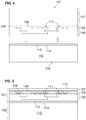
- FIG. 2-5 A simplified example manufacturing process, according to some embodiments for forming the semiconductor structure 100 of Fig. 1 , is shown by Figs. 2-5 .
- the process generally starts with the SOI wafer 101 having the insulator layer 105 (e.g. a buried oxide) between the semiconductor layer 106 and substrate layer 107 as shown in Fig. 2 .
- the first active layer 103 is then formed into and onto the "top" or "upper" surface of the semiconductor layer 106 using mostly conventional process steps. In situations where the active devices in active layer 103 are CMOS transistors, these process steps are those typically associated with single wafer monolithic CMOS manufacturing.
- the first interconnect layer 108 is then formed on the "top” or “upper” surface of the first active layer 103. Since the SOI wafer 101 is subsequently inverted from the orientation shown in Fig. 2 , for the benefit of consistency in description, the portion of the SOI wafer 101 referred to as the "top” (or “upper” or “front") with respect to Fig. 2 will continue to be referred to herein as the “top” (or “upper” or “front"), and the portion of the SOI wafer 101 referred to as the "bottom” (or “lower” or “back") will continue to be referred to herein as the “bottom” (or “lower” or “back”), even after the SOI wafer 101 has been inverted. Therefore, in Fig. 1 , the "top” of the overall semiconductor structure 100 is considered the same as the “bottom” of the SOI wafer 101. Also, when the top of the overall semiconductor structure 100 is being processed, it is considered “back side” processing for the SOI wafer 101.
- the added material or layers are considered to become part of the wafer.
- the removed material or layers are no longer considered to be part of the wafer. Therefore, for example, the element designated as the SOI wafer 101 or the handle wafer 102 in the Figs. may increase or decrease in size or thickness as it is being processed.
- a surface referred to as the "top surface” or “bottom surface” of a wafer may change during processing when material or layers are added to or removed from the wafer.
- the first active layer 103 is formed by front side processing in and on the top surface of the SOI wafer 101, but the material that is placed on the SOI wafer 101 creates a new top surface.
- the first interconnect layer 108 is formed on the new top surface. Then when the handle wafer 102 is bonded to the SOI wafer 101, it is bonded to yet another new top surface thereof.
- TSVs semiconductor vias
- the simplified example manufacturing process continues with the formation of the handle wafer 102 as shown in Fig. 3 .
- the bonding layer 113, and the TRL 114 are formed on the handle substrate layer 112.
- the handle substrate layer 112 is generally thick enough to provide structural stability or strength to the semiconductor structure 100.
- the TRL 114 is formed by any appropriate technique, e.g. implanting ions of high energy particles (e.g. a noble gas, Silicon, Oxygen, Carbon, Germanium, etc.), irradiating the handle wafer 102, depositing high resistivity material, damaging the exposed surfaces of the handle substrate layer 112, etc.
- high energy particles e.g. a noble gas, Silicon, Oxygen, Carbon, Germanium, etc.
- the bonding layer 113 may be any appropriate material that can be bonded to the material at the top surface of the SOI wafer 101. Other bonding techniques for other embodiments with or without the bonding layer 113 may also be used. In some embodiments, the bonding layer 113 may be combined with the TRL 114. In some embodiments, the entire handle wafer 102 will be the TRL 114.
- SOI wafer 101 of Fig. 2 is bonded to the handle wafer 102 of Fig. 3 .
- the SOI wafer 101 is inverted in Fig. 4 relative to its orientation in Fig. 2 .
- the surface of the SOI wafer 101 to which the handle wafer 102 is bonded is the top surface, which is opposite the insulator layer from the substrate layer 107. This step leaves the bottom or back side of the SOI wafer 101 exposed for processing.
- the handle wafer 102 provides structural stability during this processing.
- a portion of the substrate layer 107 is removed, thereby thinning the substrate layer 107, as shown in Fig. 5 .
- the remaining portion of the substrate layer 107 is sufficiently thick to be used as a new semiconductor layer for the formation of a second active layer, such as the second active layer 104 in Fig. 1 .
- a cavity 115 may be formed in the substrate layer 107.
- the cavity 115 at least partly surrounds the MEMS device 110.
- the cavity 115 may be formed by any appropriate technique, e.g. orientation dependent etch, anisotropic etch, isotropic etch, etc.
- the cavity 115 provides isolation, improved thermal performance and/or a material for release of the MEMS device 110.
- a fill material is then placed inside the cavity 115 and planarized, e.g. by CMP.
- the fill material may be selective to the material that forms second active layer 104, so the fill material can be removed later to release the MEMS device 110.
- the cavity 115 may extend into the insulator layer 105, so the fill material may have to be selective to the insulator material.
- the second active layer 104 is then formed in and on the remaining portion of the substrate layer 107.
- fabrication of the MEMS device 110 within the second active layer 104 is done in reverse order from the conventional process. This reverse process may aid in simplifying the bonding and interconnection for low temperatures (e.g. less than 200°C).
- the second interconnect layer 109 is then formed on the second active layer 104 (and through the two active layers 103 and 104) to produce the semiconductor structure 100 shown in Fig. 1 .
- some of the electrical connections between the two active layers 103 and 104 may be formed with a buried contact, e.g. forming TSVs early in the overall fabrication process.
- Electrical connection pads 116 and a redistribution layer may also be formed for external electrical connections.
- Electrical interconnects, e.g. TSVs, that pass through more than one layer may provide electrical connections between any two or more components in the two interconnect layers 108 and 109 and the active layers 103 and 104, e.g.
- TSV interconnect between metallization in the interconnect layers 108 and 109 or a TSV interconnect between metallization in one of the interconnect layers 108 or 109 and an active device (e.g. source, drain or gate region) in one of the active layers 108 or 109.
- active device e.g. source, drain or gate region
- FIG. 6 An alternative semiconductor structure 200 incorporating an alternative embodiment of the present invention is shown in Fig. 6 .
- many of the elements are similar to those of the embodiment shown in Fig. 1 , because this embodiment may be built up from the semiconductor structure 100.
- a portion of the handle substrate layer 112 is removed, thereby thinning the handle substrate layer 112.
- the remaining portion of the handle substrate layer 112 is sufficiently thick to be used as a new semiconductor layer for the formation of a third active layer 201, thereby monolithically forming yet another active layer.
- another handle wafer (not shown) may be bonded to the semiconductor structure 100 to provide structural stability during subsequent processing if the existing thickness of the semiconductor structure 100 does not provide sufficient structural stability.
- a MEMS device 202 is formed in the third active layer 201, such that a cavity 203 may need to be formed in the handle substrate layer 112.
- the cavity 203 may be formed by any appropriate technique, e.g. orientation dependent etch, anisotropic etch, isotropic etch, etc.
- the cavity 203 provides isolation, improved thermal performance and/or a material for release of the MEMS device 202.
- a fill material is then placed inside the cavity 203 and planarized, e.g. by CMP.
- the fill material may be selective to the material of third active layer 201, so the fill material can be removed later to release the MEMS device 202.
- the third active layer 201 is then formed in and on the remaining portion of the handle substrate layer 112.
- a third interconnect layer 204 is then formed on the third active layer 201 (and through to the first active layer 103) to produce the semiconductor structure 200 shown in Fig. 6 .
- some of the electrical connections between the first and third active layers 103 and 201 may be formed with a buried contact, e.g. forming TSVs early in the overall fabrication process.
- the third active layer 201 may also be connected to the second active layer 104 via contacts between those layers and a common circuit node in interconnect layer 108.
- Electrical connection pads (not shown) and a redistribution layer (not shown) may also be formed for external electrical connections on the bottom side of the alternative semiconductor structure 200.
- electrical connection pads 116 and a redistribution layer may also be formed for external electrical connections to the bottom side of the alternative semiconductor structure 200.
Landscapes
- Engineering & Computer Science (AREA)
- Manufacturing & Machinery (AREA)
- Microelectronics & Electronic Packaging (AREA)
- Computer Hardware Design (AREA)
- Power Engineering (AREA)
- General Physics & Mathematics (AREA)
- Physics & Mathematics (AREA)
- Condensed Matter Physics & Semiconductors (AREA)
- Metal-Oxide And Bipolar Metal-Oxide Semiconductor Integrated Circuits (AREA)
- Thin Film Transistor (AREA)
- Micromachines (AREA)
- Health & Medical Sciences (AREA)
- General Health & Medical Sciences (AREA)
- Toxicology (AREA)
Applications Claiming Priority (2)
| Application Number | Priority Date | Filing Date | Title |
|---|---|---|---|
| US14/454,262 US20160043108A1 (en) | 2014-08-07 | 2014-08-07 | Semiconductor Structure with Multiple Active Layers in an SOI Wafer |
| PCT/US2015/041769 WO2016022302A1 (en) | 2014-08-07 | 2015-07-23 | Semiconductor structure with multiple active layers in an soi wafer |
Publications (3)
| Publication Number | Publication Date |
|---|---|
| EP3180802A1 EP3180802A1 (en) | 2017-06-21 |
| EP3180802A4 EP3180802A4 (en) | 2018-03-07 |
| EP3180802B1 true EP3180802B1 (en) | 2020-05-06 |
Family
ID=55264334
Family Applications (1)
| Application Number | Title | Priority Date | Filing Date |
|---|---|---|---|
| EP15829048.6A Active EP3180802B1 (en) | 2014-08-07 | 2015-07-23 | Semiconductor structure with multiple active layers in an soi wafer |
Country Status (7)
| Country | Link |
|---|---|
| US (1) | US20160043108A1 (OSRAM) |
| EP (1) | EP3180802B1 (OSRAM) |
| JP (1) | JP2017526178A (OSRAM) |
| KR (1) | KR20170040226A (OSRAM) |
| CN (1) | CN106716620B (OSRAM) |
| TW (1) | TW201613035A (OSRAM) |
| WO (1) | WO2016022302A1 (OSRAM) |
Families Citing this family (3)
| Publication number | Priority date | Publication date | Assignee | Title |
|---|---|---|---|---|
| US9847293B1 (en) * | 2016-08-18 | 2017-12-19 | Qualcomm Incorporated | Utilization of backside silicidation to form dual side contacted capacitor |
| US11735585B2 (en) | 2021-01-18 | 2023-08-22 | Samsung Electronics Co., Ltd. | Stacked semiconductor device having mirror-symmetric pattern |
| CN116207036A (zh) * | 2023-02-28 | 2023-06-02 | 上海华虹宏力半导体制造有限公司 | 射频开关的形成方法 |
Family Cites Families (15)
| Publication number | Priority date | Publication date | Assignee | Title |
|---|---|---|---|---|
| JP2617798B2 (ja) * | 1989-09-22 | 1997-06-04 | 三菱電機株式会社 | 積層型半導体装置およびその製造方法 |
| KR100268419B1 (ko) * | 1998-08-14 | 2000-10-16 | 윤종용 | 고집적 반도체 메모리 장치 및 그의 제조 방법 |
| US7767484B2 (en) * | 2006-05-31 | 2010-08-03 | Georgia Tech Research Corporation | Method for sealing and backside releasing of microelectromechanical systems |
| US7485508B2 (en) * | 2007-01-26 | 2009-02-03 | International Business Machines Corporation | Two-sided semiconductor-on-insulator structures and methods of manufacturing the same |
| JP4825778B2 (ja) * | 2007-11-16 | 2011-11-30 | 株式会社日立製作所 | 半導体装置およびその製造方法 |
| US8334729B1 (en) * | 2009-03-19 | 2012-12-18 | Rf Micro Devices, Inc. | Elimination of hot switching in MEMS based impedance matching circuits |
| US9299641B2 (en) * | 2012-08-10 | 2016-03-29 | Monolithic 3D Inc. | Semiconductor system, device and structure with heat removal |
| KR101134819B1 (ko) * | 2010-07-02 | 2012-04-13 | 이상윤 | 반도체 메모리 장치의 제조 방법 |
| US8124470B1 (en) * | 2010-09-29 | 2012-02-28 | International Business Machines Corporation | Strained thin body semiconductor-on-insulator substrate and device |
| US9553013B2 (en) * | 2010-12-24 | 2017-01-24 | Qualcomm Incorporated | Semiconductor structure with TRL and handle wafer cavities |
| US8481405B2 (en) * | 2010-12-24 | 2013-07-09 | Io Semiconductor, Inc. | Trap rich layer with through-silicon-vias in semiconductor devices |
| EP3734645B1 (en) * | 2010-12-24 | 2025-09-10 | Qualcomm Incorporated | Trap rich layer for semiconductor devices |
| US9029173B2 (en) * | 2011-10-18 | 2015-05-12 | Monolithic 3D Inc. | Method for fabrication of a semiconductor device and structure |
| US9496255B2 (en) * | 2011-11-16 | 2016-11-15 | Qualcomm Incorporated | Stacked CMOS chipset having an insulating layer and a secondary layer and method of forming same |
| CN104249991B (zh) * | 2013-06-26 | 2016-08-10 | 中芯国际集成电路制造(上海)有限公司 | Mems器件及其制作方法 |
-
2014
- 2014-08-07 US US14/454,262 patent/US20160043108A1/en not_active Abandoned
-
2015
- 2015-07-23 KR KR1020177002990A patent/KR20170040226A/ko not_active Withdrawn
- 2015-07-23 JP JP2017505838A patent/JP2017526178A/ja active Pending
- 2015-07-23 WO PCT/US2015/041769 patent/WO2016022302A1/en not_active Ceased
- 2015-07-23 CN CN201580042310.2A patent/CN106716620B/zh not_active Expired - Fee Related
- 2015-07-23 EP EP15829048.6A patent/EP3180802B1/en active Active
- 2015-07-24 TW TW104124120A patent/TW201613035A/zh unknown
Non-Patent Citations (1)
| Title |
|---|
| None * |
Also Published As
| Publication number | Publication date |
|---|---|
| EP3180802A1 (en) | 2017-06-21 |
| TW201613035A (en) | 2016-04-01 |
| JP2017526178A (ja) | 2017-09-07 |
| WO2016022302A1 (en) | 2016-02-11 |
| KR20170040226A (ko) | 2017-04-12 |
| CN106716620A (zh) | 2017-05-24 |
| EP3180802A4 (en) | 2018-03-07 |
| US20160043108A1 (en) | 2016-02-11 |
| CN106716620B (zh) | 2020-09-08 |
Similar Documents
| Publication | Publication Date | Title |
|---|---|---|
| US7183176B2 (en) | Method of forming through-wafer interconnects for vertical wafer level packaging | |
| US9922956B2 (en) | Microelectromechanical system (MEMS) bond release structure and method of wafer transfer for three-dimensional integrated circuit (3D IC) integration | |
| EP1851797B1 (en) | Device and method for fabricating double-sided soi wafer scale package with through via connections | |
| US8629553B2 (en) | 3D integrated circuit device fabrication with precisely controllable substrate removal | |
| US8922026B2 (en) | Chip package and fabrication method thereof | |
| US7935571B2 (en) | Through substrate vias for back-side interconnections on very thin semiconductor wafers | |
| US8563396B2 (en) | 3D integration method using SOI substrates and structures produced thereby | |
| CN116391252A (zh) | 具有互连结构的键合结构 | |
| US8298914B2 (en) | 3D integrated circuit device fabrication using interface wafer as permanent carrier | |
| US9511996B2 (en) | Methods of forming semiconductor structures including MEMS devices and integrated circuits on common sides of substrates, and related structures and devices | |
| WO2011066742A1 (zh) | 3d集成电路结构、半导体器件及其形成方法 | |
| US9481566B2 (en) | Methods of forming semiconductor structures including MEMS devices and integrated circuits on opposing sides of substrates, and related structures and devices | |
| EP3180802B1 (en) | Semiconductor structure with multiple active layers in an soi wafer | |
| CN117623216A (zh) | 一种mems器件及其制备方法、电子装置 | |
| CN107369649B (zh) | 一种半导体器件及其制造方法 |
Legal Events
| Date | Code | Title | Description |
|---|---|---|---|
| STAA | Information on the status of an ep patent application or granted ep patent |
Free format text: STATUS: THE INTERNATIONAL PUBLICATION HAS BEEN MADE |
|
| PUAI | Public reference made under article 153(3) epc to a published international application that has entered the european phase |
Free format text: ORIGINAL CODE: 0009012 |
|
| STAA | Information on the status of an ep patent application or granted ep patent |
Free format text: STATUS: REQUEST FOR EXAMINATION WAS MADE |
|
| 17P | Request for examination filed |
Effective date: 20170106 |
|
| AK | Designated contracting states |
Kind code of ref document: A1 Designated state(s): AL AT BE BG CH CY CZ DE DK EE ES FI FR GB GR HR HU IE IS IT LI LT LU LV MC MK MT NL NO PL PT RO RS SE SI SK SM TR |
|
| AX | Request for extension of the european patent |
Extension state: BA ME |
|
| DAV | Request for validation of the european patent (deleted) | ||
| DAX | Request for extension of the european patent (deleted) | ||
| A4 | Supplementary search report drawn up and despatched |
Effective date: 20180201 |
|
| RIC1 | Information provided on ipc code assigned before grant |
Ipc: H01L 21/8238 20060101ALI20180126BHEP Ipc: B81C 1/00 20060101ALI20180126BHEP Ipc: H01L 23/485 20060101ALI20180126BHEP Ipc: H01L 21/762 20060101AFI20180126BHEP |
|
| STAA | Information on the status of an ep patent application or granted ep patent |
Free format text: STATUS: EXAMINATION IS IN PROGRESS |
|
| 17Q | First examination report despatched |
Effective date: 20190221 |
|
| GRAP | Despatch of communication of intention to grant a patent |
Free format text: ORIGINAL CODE: EPIDOSNIGR1 |
|
| STAA | Information on the status of an ep patent application or granted ep patent |
Free format text: STATUS: GRANT OF PATENT IS INTENDED |
|
| INTG | Intention to grant announced |
Effective date: 20191203 |
|
| GRAS | Grant fee paid |
Free format text: ORIGINAL CODE: EPIDOSNIGR3 |
|
| GRAA | (expected) grant |
Free format text: ORIGINAL CODE: 0009210 |
|
| STAA | Information on the status of an ep patent application or granted ep patent |
Free format text: STATUS: THE PATENT HAS BEEN GRANTED |
|
| AK | Designated contracting states |
Kind code of ref document: B1 Designated state(s): AL AT BE BG CH CY CZ DE DK EE ES FI FR GB GR HR HU IE IS IT LI LT LU LV MC MK MT NL NO PL PT RO RS SE SI SK SM TR |
|
| REG | Reference to a national code |
Ref country code: GB Ref legal event code: FG4D |
|
| REG | Reference to a national code |
Ref country code: CH Ref legal event code: EP Ref country code: AT Ref legal event code: REF Ref document number: 1268172 Country of ref document: AT Kind code of ref document: T Effective date: 20200515 |
|
| REG | Reference to a national code |
Ref country code: IE Ref legal event code: FG4D |
|
| REG | Reference to a national code |
Ref country code: DE Ref legal event code: R096 Ref document number: 602015052448 Country of ref document: DE |
|
| REG | Reference to a national code |
Ref country code: LT Ref legal event code: MG4D |
|
| REG | Reference to a national code |
Ref country code: NL Ref legal event code: MP Effective date: 20200506 |
|
| PG25 | Lapsed in a contracting state [announced via postgrant information from national office to epo] |
Ref country code: IS Free format text: LAPSE BECAUSE OF FAILURE TO SUBMIT A TRANSLATION OF THE DESCRIPTION OR TO PAY THE FEE WITHIN THE PRESCRIBED TIME-LIMIT Effective date: 20200906 Ref country code: PT Free format text: LAPSE BECAUSE OF FAILURE TO SUBMIT A TRANSLATION OF THE DESCRIPTION OR TO PAY THE FEE WITHIN THE PRESCRIBED TIME-LIMIT Effective date: 20200907 Ref country code: FI Free format text: LAPSE BECAUSE OF FAILURE TO SUBMIT A TRANSLATION OF THE DESCRIPTION OR TO PAY THE FEE WITHIN THE PRESCRIBED TIME-LIMIT Effective date: 20200506 Ref country code: GR Free format text: LAPSE BECAUSE OF FAILURE TO SUBMIT A TRANSLATION OF THE DESCRIPTION OR TO PAY THE FEE WITHIN THE PRESCRIBED TIME-LIMIT Effective date: 20200807 Ref country code: NO Free format text: LAPSE BECAUSE OF FAILURE TO SUBMIT A TRANSLATION OF THE DESCRIPTION OR TO PAY THE FEE WITHIN THE PRESCRIBED TIME-LIMIT Effective date: 20200806 Ref country code: SE Free format text: LAPSE BECAUSE OF FAILURE TO SUBMIT A TRANSLATION OF THE DESCRIPTION OR TO PAY THE FEE WITHIN THE PRESCRIBED TIME-LIMIT Effective date: 20200506 Ref country code: LT Free format text: LAPSE BECAUSE OF FAILURE TO SUBMIT A TRANSLATION OF THE DESCRIPTION OR TO PAY THE FEE WITHIN THE PRESCRIBED TIME-LIMIT Effective date: 20200506 |
|
| PG25 | Lapsed in a contracting state [announced via postgrant information from national office to epo] |
Ref country code: BG Free format text: LAPSE BECAUSE OF FAILURE TO SUBMIT A TRANSLATION OF THE DESCRIPTION OR TO PAY THE FEE WITHIN THE PRESCRIBED TIME-LIMIT Effective date: 20200806 Ref country code: HR Free format text: LAPSE BECAUSE OF FAILURE TO SUBMIT A TRANSLATION OF THE DESCRIPTION OR TO PAY THE FEE WITHIN THE PRESCRIBED TIME-LIMIT Effective date: 20200506 Ref country code: LV Free format text: LAPSE BECAUSE OF FAILURE TO SUBMIT A TRANSLATION OF THE DESCRIPTION OR TO PAY THE FEE WITHIN THE PRESCRIBED TIME-LIMIT Effective date: 20200506 Ref country code: RS Free format text: LAPSE BECAUSE OF FAILURE TO SUBMIT A TRANSLATION OF THE DESCRIPTION OR TO PAY THE FEE WITHIN THE PRESCRIBED TIME-LIMIT Effective date: 20200506 |
|
| REG | Reference to a national code |
Ref country code: AT Ref legal event code: MK05 Ref document number: 1268172 Country of ref document: AT Kind code of ref document: T Effective date: 20200506 |
|
| PG25 | Lapsed in a contracting state [announced via postgrant information from national office to epo] |
Ref country code: AL Free format text: LAPSE BECAUSE OF FAILURE TO SUBMIT A TRANSLATION OF THE DESCRIPTION OR TO PAY THE FEE WITHIN THE PRESCRIBED TIME-LIMIT Effective date: 20200506 Ref country code: NL Free format text: LAPSE BECAUSE OF FAILURE TO SUBMIT A TRANSLATION OF THE DESCRIPTION OR TO PAY THE FEE WITHIN THE PRESCRIBED TIME-LIMIT Effective date: 20200506 |
|
| PG25 | Lapsed in a contracting state [announced via postgrant information from national office to epo] |
Ref country code: DK Free format text: LAPSE BECAUSE OF FAILURE TO SUBMIT A TRANSLATION OF THE DESCRIPTION OR TO PAY THE FEE WITHIN THE PRESCRIBED TIME-LIMIT Effective date: 20200506 Ref country code: AT Free format text: LAPSE BECAUSE OF FAILURE TO SUBMIT A TRANSLATION OF THE DESCRIPTION OR TO PAY THE FEE WITHIN THE PRESCRIBED TIME-LIMIT Effective date: 20200506 Ref country code: ES Free format text: LAPSE BECAUSE OF FAILURE TO SUBMIT A TRANSLATION OF THE DESCRIPTION OR TO PAY THE FEE WITHIN THE PRESCRIBED TIME-LIMIT Effective date: 20200506 Ref country code: CZ Free format text: LAPSE BECAUSE OF FAILURE TO SUBMIT A TRANSLATION OF THE DESCRIPTION OR TO PAY THE FEE WITHIN THE PRESCRIBED TIME-LIMIT Effective date: 20200506 Ref country code: RO Free format text: LAPSE BECAUSE OF FAILURE TO SUBMIT A TRANSLATION OF THE DESCRIPTION OR TO PAY THE FEE WITHIN THE PRESCRIBED TIME-LIMIT Effective date: 20200506 Ref country code: IT Free format text: LAPSE BECAUSE OF FAILURE TO SUBMIT A TRANSLATION OF THE DESCRIPTION OR TO PAY THE FEE WITHIN THE PRESCRIBED TIME-LIMIT Effective date: 20200506 Ref country code: SM Free format text: LAPSE BECAUSE OF FAILURE TO SUBMIT A TRANSLATION OF THE DESCRIPTION OR TO PAY THE FEE WITHIN THE PRESCRIBED TIME-LIMIT Effective date: 20200506 Ref country code: EE Free format text: LAPSE BECAUSE OF FAILURE TO SUBMIT A TRANSLATION OF THE DESCRIPTION OR TO PAY THE FEE WITHIN THE PRESCRIBED TIME-LIMIT Effective date: 20200506 |
|
| REG | Reference to a national code |
Ref country code: DE Ref legal event code: R097 Ref document number: 602015052448 Country of ref document: DE |
|
| PG25 | Lapsed in a contracting state [announced via postgrant information from national office to epo] |
Ref country code: PL Free format text: LAPSE BECAUSE OF FAILURE TO SUBMIT A TRANSLATION OF THE DESCRIPTION OR TO PAY THE FEE WITHIN THE PRESCRIBED TIME-LIMIT Effective date: 20200506 Ref country code: SK Free format text: LAPSE BECAUSE OF FAILURE TO SUBMIT A TRANSLATION OF THE DESCRIPTION OR TO PAY THE FEE WITHIN THE PRESCRIBED TIME-LIMIT Effective date: 20200506 Ref country code: MC Free format text: LAPSE BECAUSE OF FAILURE TO SUBMIT A TRANSLATION OF THE DESCRIPTION OR TO PAY THE FEE WITHIN THE PRESCRIBED TIME-LIMIT Effective date: 20200506 |
|
| REG | Reference to a national code |
Ref country code: CH Ref legal event code: PL |
|
| PLBE | No opposition filed within time limit |
Free format text: ORIGINAL CODE: 0009261 |
|
| STAA | Information on the status of an ep patent application or granted ep patent |
Free format text: STATUS: NO OPPOSITION FILED WITHIN TIME LIMIT |
|
| 26N | No opposition filed |
Effective date: 20210209 |
|
| REG | Reference to a national code |
Ref country code: BE Ref legal event code: MM Effective date: 20200731 |
|
| PG25 | Lapsed in a contracting state [announced via postgrant information from national office to epo] |
Ref country code: LI Free format text: LAPSE BECAUSE OF NON-PAYMENT OF DUE FEES Effective date: 20200731 Ref country code: LU Free format text: LAPSE BECAUSE OF NON-PAYMENT OF DUE FEES Effective date: 20200723 Ref country code: CH Free format text: LAPSE BECAUSE OF NON-PAYMENT OF DUE FEES Effective date: 20200731 |
|
| PG25 | Lapsed in a contracting state [announced via postgrant information from national office to epo] |
Ref country code: BE Free format text: LAPSE BECAUSE OF NON-PAYMENT OF DUE FEES Effective date: 20200731 Ref country code: SI Free format text: LAPSE BECAUSE OF FAILURE TO SUBMIT A TRANSLATION OF THE DESCRIPTION OR TO PAY THE FEE WITHIN THE PRESCRIBED TIME-LIMIT Effective date: 20200506 |
|
| PG25 | Lapsed in a contracting state [announced via postgrant information from national office to epo] |
Ref country code: IE Free format text: LAPSE BECAUSE OF NON-PAYMENT OF DUE FEES Effective date: 20200723 |
|
| PG25 | Lapsed in a contracting state [announced via postgrant information from national office to epo] |
Ref country code: TR Free format text: LAPSE BECAUSE OF FAILURE TO SUBMIT A TRANSLATION OF THE DESCRIPTION OR TO PAY THE FEE WITHIN THE PRESCRIBED TIME-LIMIT Effective date: 20200506 Ref country code: MT Free format text: LAPSE BECAUSE OF FAILURE TO SUBMIT A TRANSLATION OF THE DESCRIPTION OR TO PAY THE FEE WITHIN THE PRESCRIBED TIME-LIMIT Effective date: 20200506 Ref country code: CY Free format text: LAPSE BECAUSE OF FAILURE TO SUBMIT A TRANSLATION OF THE DESCRIPTION OR TO PAY THE FEE WITHIN THE PRESCRIBED TIME-LIMIT Effective date: 20200506 |
|
| PG25 | Lapsed in a contracting state [announced via postgrant information from national office to epo] |
Ref country code: MK Free format text: LAPSE BECAUSE OF FAILURE TO SUBMIT A TRANSLATION OF THE DESCRIPTION OR TO PAY THE FEE WITHIN THE PRESCRIBED TIME-LIMIT Effective date: 20200506 |
|
| PGFP | Annual fee paid to national office [announced via postgrant information from national office to epo] |
Ref country code: GB Payment date: 20240613 Year of fee payment: 10 |
|
| PGFP | Annual fee paid to national office [announced via postgrant information from national office to epo] |
Ref country code: FR Payment date: 20240613 Year of fee payment: 10 |
|
| PGFP | Annual fee paid to national office [announced via postgrant information from national office to epo] |
Ref country code: DE Payment date: 20250616 Year of fee payment: 11 |