US11735585B2 - Stacked semiconductor device having mirror-symmetric pattern - Google Patents
Stacked semiconductor device having mirror-symmetric pattern Download PDFInfo
- Publication number
- US11735585B2 US11735585B2 US17/223,829 US202117223829A US11735585B2 US 11735585 B2 US11735585 B2 US 11735585B2 US 202117223829 A US202117223829 A US 202117223829A US 11735585 B2 US11735585 B2 US 11735585B2
- Authority
- US
- United States
- Prior art keywords
- active region
- gate structure
- transistor
- semiconductor device
- stacked semiconductor
- Prior art date
- Legal status (The legal status is an assumption and is not a legal conclusion. Google has not performed a legal analysis and makes no representation as to the accuracy of the status listed.)
- Active, expires
Links
- 239000004065 semiconductor Substances 0.000 title claims abstract description 140
- 239000000758 substrate Substances 0.000 claims abstract description 54
- 239000010410 layer Substances 0.000 claims description 166
- 238000002955 isolation Methods 0.000 claims description 66
- 239000002184 metal Substances 0.000 claims description 40
- 229910052751 metal Inorganic materials 0.000 claims description 40
- 239000002135 nanosheet Substances 0.000 claims description 28
- 229910044991 metal oxide Inorganic materials 0.000 claims description 13
- 150000004706 metal oxides Chemical class 0.000 claims description 13
- 239000000463 material Substances 0.000 claims description 12
- 229910052710 silicon Inorganic materials 0.000 claims description 4
- 239000010703 silicon Substances 0.000 claims description 4
- 230000005669 field effect Effects 0.000 claims description 3
- 239000011229 interlayer Substances 0.000 claims description 3
- 239000011800 void material Substances 0.000 description 37
- 238000000034 method Methods 0.000 description 26
- 238000004519 manufacturing process Methods 0.000 description 16
- 230000015572 biosynthetic process Effects 0.000 description 9
- VYPSYNLAJGMNEJ-UHFFFAOYSA-N Silicium dioxide Chemical compound O=[Si]=O VYPSYNLAJGMNEJ-UHFFFAOYSA-N 0.000 description 7
- 238000000137 annealing Methods 0.000 description 7
- 238000001020 plasma etching Methods 0.000 description 7
- 238000001312 dry etching Methods 0.000 description 6
- 230000006870 function Effects 0.000 description 6
- 229910052782 aluminium Inorganic materials 0.000 description 4
- 239000003989 dielectric material Substances 0.000 description 4
- 239000000126 substance Substances 0.000 description 4
- 229910052719 titanium Inorganic materials 0.000 description 4
- 238000001039 wet etching Methods 0.000 description 4
- ITWBWJFEJCHKSN-UHFFFAOYSA-N 1,4,7-triazonane Chemical compound C1CNCCNCCN1 ITWBWJFEJCHKSN-UHFFFAOYSA-N 0.000 description 3
- 229910004166 TaN Inorganic materials 0.000 description 3
- 229910004200 TaSiN Inorganic materials 0.000 description 3
- 229910010038 TiAl Inorganic materials 0.000 description 3
- 229910010041 TiAlC Inorganic materials 0.000 description 3
- 229910010037 TiAlN Inorganic materials 0.000 description 3
- 229910034327 TiC Inorganic materials 0.000 description 3
- ATJFFYVFTNAWJD-UHFFFAOYSA-N Tin Chemical compound [Sn] ATJFFYVFTNAWJD-UHFFFAOYSA-N 0.000 description 3
- 238000000231 atomic layer deposition Methods 0.000 description 3
- 229910052802 copper Inorganic materials 0.000 description 3
- 238000002513 implantation Methods 0.000 description 3
- 239000000377 silicon dioxide Substances 0.000 description 3
- 229910003468 tantalcarbide Inorganic materials 0.000 description 3
- 229910052715 tantalum Inorganic materials 0.000 description 3
- 229910052721 tungsten Inorganic materials 0.000 description 3
- XUIMIQQOPSSXEZ-UHFFFAOYSA-N Silicon Chemical compound [Si] XUIMIQQOPSSXEZ-UHFFFAOYSA-N 0.000 description 2
- 229910000577 Silicon-germanium Inorganic materials 0.000 description 2
- 238000005229 chemical vapour deposition Methods 0.000 description 2
- 238000004891 communication Methods 0.000 description 2
- 238000010586 diagram Methods 0.000 description 2
- 230000014509 gene expression Effects 0.000 description 2
- 239000012212 insulator Substances 0.000 description 2
- 238000005240 physical vapour deposition Methods 0.000 description 2
- 229910021420 polycrystalline silicon Inorganic materials 0.000 description 2
- 229920005591 polysilicon Polymers 0.000 description 2
- 235000012239 silicon dioxide Nutrition 0.000 description 2
- 229920001621 AMOLED Polymers 0.000 description 1
- OKTJSMMVPCPJKN-UHFFFAOYSA-N Carbon Chemical compound [C] OKTJSMMVPCPJKN-UHFFFAOYSA-N 0.000 description 1
- 229910052581 Si3N4 Inorganic materials 0.000 description 1
- LEVVHYCKPQWKOP-UHFFFAOYSA-N [Si].[Ge] Chemical compound [Si].[Ge] LEVVHYCKPQWKOP-UHFFFAOYSA-N 0.000 description 1
- 229910003481 amorphous carbon Inorganic materials 0.000 description 1
- 229910021417 amorphous silicon Inorganic materials 0.000 description 1
- 229910052788 barium Inorganic materials 0.000 description 1
- 229910052799 carbon Inorganic materials 0.000 description 1
- 239000012141 concentrate Substances 0.000 description 1
- 238000005530 etching Methods 0.000 description 1
- -1 for example Substances 0.000 description 1
- 229910052732 germanium Inorganic materials 0.000 description 1
- GNPVGFCGXDBREM-UHFFFAOYSA-N germanium atom Chemical compound [Ge] GNPVGFCGXDBREM-UHFFFAOYSA-N 0.000 description 1
- 229910052735 hafnium Inorganic materials 0.000 description 1
- 239000007943 implant Substances 0.000 description 1
- 239000012535 impurity Substances 0.000 description 1
- 229910052746 lanthanum Inorganic materials 0.000 description 1
- 229910052745 lead Inorganic materials 0.000 description 1
- 239000004973 liquid crystal related substance Substances 0.000 description 1
- 238000001459 lithography Methods 0.000 description 1
- 229910052749 magnesium Inorganic materials 0.000 description 1
- 239000011159 matrix material Substances 0.000 description 1
- 229910052914 metal silicate Inorganic materials 0.000 description 1
- 238000012986 modification Methods 0.000 description 1
- 230000004048 modification Effects 0.000 description 1
- 230000003252 repetitive effect Effects 0.000 description 1
- LIVNPJMFVYWSIS-UHFFFAOYSA-N silicon monoxide Chemical compound [Si-]#[O+] LIVNPJMFVYWSIS-UHFFFAOYSA-N 0.000 description 1
- HQVNEWCFYHHQES-UHFFFAOYSA-N silicon nitride Chemical compound N12[Si]34N5[Si]62N3[Si]51N64 HQVNEWCFYHHQES-UHFFFAOYSA-N 0.000 description 1
- 229910052814 silicon oxide Inorganic materials 0.000 description 1
- 239000007787 solid Substances 0.000 description 1
- 230000003068 static effect Effects 0.000 description 1
- 229910052726 zirconium Inorganic materials 0.000 description 1
Images


Classifications
-
- H—ELECTRICITY
- H01—ELECTRIC ELEMENTS
- H01L—SEMICONDUCTOR DEVICES NOT COVERED BY CLASS H10
- H01L27/00—Devices consisting of a plurality of semiconductor or other solid-state components formed in or on a common substrate
- H01L27/02—Devices consisting of a plurality of semiconductor or other solid-state components formed in or on a common substrate including semiconductor components specially adapted for rectifying, oscillating, amplifying or switching and having at least one potential-jump barrier or surface barrier; including integrated passive circuit elements with at least one potential-jump barrier or surface barrier
- H01L27/04—Devices consisting of a plurality of semiconductor or other solid-state components formed in or on a common substrate including semiconductor components specially adapted for rectifying, oscillating, amplifying or switching and having at least one potential-jump barrier or surface barrier; including integrated passive circuit elements with at least one potential-jump barrier or surface barrier the substrate being a semiconductor body
- H01L27/08—Devices consisting of a plurality of semiconductor or other solid-state components formed in or on a common substrate including semiconductor components specially adapted for rectifying, oscillating, amplifying or switching and having at least one potential-jump barrier or surface barrier; including integrated passive circuit elements with at least one potential-jump barrier or surface barrier the substrate being a semiconductor body including only semiconductor components of a single kind
- H01L27/085—Devices consisting of a plurality of semiconductor or other solid-state components formed in or on a common substrate including semiconductor components specially adapted for rectifying, oscillating, amplifying or switching and having at least one potential-jump barrier or surface barrier; including integrated passive circuit elements with at least one potential-jump barrier or surface barrier the substrate being a semiconductor body including only semiconductor components of a single kind including field-effect components only
- H01L27/088—Devices consisting of a plurality of semiconductor or other solid-state components formed in or on a common substrate including semiconductor components specially adapted for rectifying, oscillating, amplifying or switching and having at least one potential-jump barrier or surface barrier; including integrated passive circuit elements with at least one potential-jump barrier or surface barrier the substrate being a semiconductor body including only semiconductor components of a single kind including field-effect components only the components being field-effect transistors with insulated gate
-
- H—ELECTRICITY
- H01—ELECTRIC ELEMENTS
- H01L—SEMICONDUCTOR DEVICES NOT COVERED BY CLASS H10
- H01L27/00—Devices consisting of a plurality of semiconductor or other solid-state components formed in or on a common substrate
- H01L27/02—Devices consisting of a plurality of semiconductor or other solid-state components formed in or on a common substrate including semiconductor components specially adapted for rectifying, oscillating, amplifying or switching and having at least one potential-jump barrier or surface barrier; including integrated passive circuit elements with at least one potential-jump barrier or surface barrier
- H01L27/04—Devices consisting of a plurality of semiconductor or other solid-state components formed in or on a common substrate including semiconductor components specially adapted for rectifying, oscillating, amplifying or switching and having at least one potential-jump barrier or surface barrier; including integrated passive circuit elements with at least one potential-jump barrier or surface barrier the substrate being a semiconductor body
- H01L27/06—Devices consisting of a plurality of semiconductor or other solid-state components formed in or on a common substrate including semiconductor components specially adapted for rectifying, oscillating, amplifying or switching and having at least one potential-jump barrier or surface barrier; including integrated passive circuit elements with at least one potential-jump barrier or surface barrier the substrate being a semiconductor body including a plurality of individual components in a non-repetitive configuration
- H01L27/0688—Integrated circuits having a three-dimensional layout
-
- H—ELECTRICITY
- H01—ELECTRIC ELEMENTS
- H01L—SEMICONDUCTOR DEVICES NOT COVERED BY CLASS H10
- H01L21/00—Processes or apparatus adapted for the manufacture or treatment of semiconductor or solid state devices or of parts thereof
- H01L21/70—Manufacture or treatment of devices consisting of a plurality of solid state components formed in or on a common substrate or of parts thereof; Manufacture of integrated circuit devices or of parts thereof
- H01L21/77—Manufacture or treatment of devices consisting of a plurality of solid state components or integrated circuits formed in, or on, a common substrate
- H01L21/78—Manufacture or treatment of devices consisting of a plurality of solid state components or integrated circuits formed in, or on, a common substrate with subsequent division of the substrate into plural individual devices
- H01L21/82—Manufacture or treatment of devices consisting of a plurality of solid state components or integrated circuits formed in, or on, a common substrate with subsequent division of the substrate into plural individual devices to produce devices, e.g. integrated circuits, each consisting of a plurality of components
- H01L21/822—Manufacture or treatment of devices consisting of a plurality of solid state components or integrated circuits formed in, or on, a common substrate with subsequent division of the substrate into plural individual devices to produce devices, e.g. integrated circuits, each consisting of a plurality of components the substrate being a semiconductor, using silicon technology
- H01L21/8221—Three dimensional integrated circuits stacked in different levels
-
- H—ELECTRICITY
- H01—ELECTRIC ELEMENTS
- H01L—SEMICONDUCTOR DEVICES NOT COVERED BY CLASS H10
- H01L21/00—Processes or apparatus adapted for the manufacture or treatment of semiconductor or solid state devices or of parts thereof
- H01L21/70—Manufacture or treatment of devices consisting of a plurality of solid state components formed in or on a common substrate or of parts thereof; Manufacture of integrated circuit devices or of parts thereof
- H01L21/77—Manufacture or treatment of devices consisting of a plurality of solid state components or integrated circuits formed in, or on, a common substrate
- H01L21/78—Manufacture or treatment of devices consisting of a plurality of solid state components or integrated circuits formed in, or on, a common substrate with subsequent division of the substrate into plural individual devices
- H01L21/82—Manufacture or treatment of devices consisting of a plurality of solid state components or integrated circuits formed in, or on, a common substrate with subsequent division of the substrate into plural individual devices to produce devices, e.g. integrated circuits, each consisting of a plurality of components
- H01L21/822—Manufacture or treatment of devices consisting of a plurality of solid state components or integrated circuits formed in, or on, a common substrate with subsequent division of the substrate into plural individual devices to produce devices, e.g. integrated circuits, each consisting of a plurality of components the substrate being a semiconductor, using silicon technology
- H01L21/8232—Field-effect technology
- H01L21/8234—MIS technology, i.e. integration processes of field effect transistors of the conductor-insulator-semiconductor type
- H01L21/823412—MIS technology, i.e. integration processes of field effect transistors of the conductor-insulator-semiconductor type with a particular manufacturing method of the channel structures, e.g. channel implants, halo or pocket implants, or channel materials
-
- H—ELECTRICITY
- H01—ELECTRIC ELEMENTS
- H01L—SEMICONDUCTOR DEVICES NOT COVERED BY CLASS H10
- H01L21/00—Processes or apparatus adapted for the manufacture or treatment of semiconductor or solid state devices or of parts thereof
- H01L21/70—Manufacture or treatment of devices consisting of a plurality of solid state components formed in or on a common substrate or of parts thereof; Manufacture of integrated circuit devices or of parts thereof
- H01L21/77—Manufacture or treatment of devices consisting of a plurality of solid state components or integrated circuits formed in, or on, a common substrate
- H01L21/78—Manufacture or treatment of devices consisting of a plurality of solid state components or integrated circuits formed in, or on, a common substrate with subsequent division of the substrate into plural individual devices
- H01L21/82—Manufacture or treatment of devices consisting of a plurality of solid state components or integrated circuits formed in, or on, a common substrate with subsequent division of the substrate into plural individual devices to produce devices, e.g. integrated circuits, each consisting of a plurality of components
- H01L21/822—Manufacture or treatment of devices consisting of a plurality of solid state components or integrated circuits formed in, or on, a common substrate with subsequent division of the substrate into plural individual devices to produce devices, e.g. integrated circuits, each consisting of a plurality of components the substrate being a semiconductor, using silicon technology
- H01L21/8232—Field-effect technology
- H01L21/8234—MIS technology, i.e. integration processes of field effect transistors of the conductor-insulator-semiconductor type
- H01L21/823418—MIS technology, i.e. integration processes of field effect transistors of the conductor-insulator-semiconductor type with a particular manufacturing method of the source or drain structures, e.g. specific source or drain implants or silicided source or drain structures or raised source or drain structures
-
- H—ELECTRICITY
- H01—ELECTRIC ELEMENTS
- H01L—SEMICONDUCTOR DEVICES NOT COVERED BY CLASS H10
- H01L21/00—Processes or apparatus adapted for the manufacture or treatment of semiconductor or solid state devices or of parts thereof
- H01L21/70—Manufacture or treatment of devices consisting of a plurality of solid state components formed in or on a common substrate or of parts thereof; Manufacture of integrated circuit devices or of parts thereof
- H01L21/77—Manufacture or treatment of devices consisting of a plurality of solid state components or integrated circuits formed in, or on, a common substrate
- H01L21/78—Manufacture or treatment of devices consisting of a plurality of solid state components or integrated circuits formed in, or on, a common substrate with subsequent division of the substrate into plural individual devices
- H01L21/82—Manufacture or treatment of devices consisting of a plurality of solid state components or integrated circuits formed in, or on, a common substrate with subsequent division of the substrate into plural individual devices to produce devices, e.g. integrated circuits, each consisting of a plurality of components
- H01L21/822—Manufacture or treatment of devices consisting of a plurality of solid state components or integrated circuits formed in, or on, a common substrate with subsequent division of the substrate into plural individual devices to produce devices, e.g. integrated circuits, each consisting of a plurality of components the substrate being a semiconductor, using silicon technology
- H01L21/8232—Field-effect technology
- H01L21/8234—MIS technology, i.e. integration processes of field effect transistors of the conductor-insulator-semiconductor type
- H01L21/823431—MIS technology, i.e. integration processes of field effect transistors of the conductor-insulator-semiconductor type with a particular manufacturing method of transistors with a horizontal current flow in a vertical sidewall of a semiconductor body, e.g. FinFET, MuGFET
-
- H—ELECTRICITY
- H01—ELECTRIC ELEMENTS
- H01L—SEMICONDUCTOR DEVICES NOT COVERED BY CLASS H10
- H01L21/00—Processes or apparatus adapted for the manufacture or treatment of semiconductor or solid state devices or of parts thereof
- H01L21/70—Manufacture or treatment of devices consisting of a plurality of solid state components formed in or on a common substrate or of parts thereof; Manufacture of integrated circuit devices or of parts thereof
- H01L21/77—Manufacture or treatment of devices consisting of a plurality of solid state components or integrated circuits formed in, or on, a common substrate
- H01L21/78—Manufacture or treatment of devices consisting of a plurality of solid state components or integrated circuits formed in, or on, a common substrate with subsequent division of the substrate into plural individual devices
- H01L21/82—Manufacture or treatment of devices consisting of a plurality of solid state components or integrated circuits formed in, or on, a common substrate with subsequent division of the substrate into plural individual devices to produce devices, e.g. integrated circuits, each consisting of a plurality of components
- H01L21/822—Manufacture or treatment of devices consisting of a plurality of solid state components or integrated circuits formed in, or on, a common substrate with subsequent division of the substrate into plural individual devices to produce devices, e.g. integrated circuits, each consisting of a plurality of components the substrate being a semiconductor, using silicon technology
- H01L21/8232—Field-effect technology
- H01L21/8234—MIS technology, i.e. integration processes of field effect transistors of the conductor-insulator-semiconductor type
- H01L21/823437—MIS technology, i.e. integration processes of field effect transistors of the conductor-insulator-semiconductor type with a particular manufacturing method of the gate conductors, e.g. particular materials, shapes
-
- H—ELECTRICITY
- H01—ELECTRIC ELEMENTS
- H01L—SEMICONDUCTOR DEVICES NOT COVERED BY CLASS H10
- H01L21/00—Processes or apparatus adapted for the manufacture or treatment of semiconductor or solid state devices or of parts thereof
- H01L21/70—Manufacture or treatment of devices consisting of a plurality of solid state components formed in or on a common substrate or of parts thereof; Manufacture of integrated circuit devices or of parts thereof
- H01L21/77—Manufacture or treatment of devices consisting of a plurality of solid state components or integrated circuits formed in, or on, a common substrate
- H01L21/78—Manufacture or treatment of devices consisting of a plurality of solid state components or integrated circuits formed in, or on, a common substrate with subsequent division of the substrate into plural individual devices
- H01L21/82—Manufacture or treatment of devices consisting of a plurality of solid state components or integrated circuits formed in, or on, a common substrate with subsequent division of the substrate into plural individual devices to produce devices, e.g. integrated circuits, each consisting of a plurality of components
- H01L21/822—Manufacture or treatment of devices consisting of a plurality of solid state components or integrated circuits formed in, or on, a common substrate with subsequent division of the substrate into plural individual devices to produce devices, e.g. integrated circuits, each consisting of a plurality of components the substrate being a semiconductor, using silicon technology
- H01L21/8232—Field-effect technology
- H01L21/8234—MIS technology, i.e. integration processes of field effect transistors of the conductor-insulator-semiconductor type
- H01L21/823475—MIS technology, i.e. integration processes of field effect transistors of the conductor-insulator-semiconductor type interconnection or wiring or contact manufacturing related aspects
-
- H—ELECTRICITY
- H01—ELECTRIC ELEMENTS
- H01L—SEMICONDUCTOR DEVICES NOT COVERED BY CLASS H10
- H01L21/00—Processes or apparatus adapted for the manufacture or treatment of semiconductor or solid state devices or of parts thereof
- H01L21/70—Manufacture or treatment of devices consisting of a plurality of solid state components formed in or on a common substrate or of parts thereof; Manufacture of integrated circuit devices or of parts thereof
- H01L21/77—Manufacture or treatment of devices consisting of a plurality of solid state components or integrated circuits formed in, or on, a common substrate
- H01L21/78—Manufacture or treatment of devices consisting of a plurality of solid state components or integrated circuits formed in, or on, a common substrate with subsequent division of the substrate into plural individual devices
- H01L21/82—Manufacture or treatment of devices consisting of a plurality of solid state components or integrated circuits formed in, or on, a common substrate with subsequent division of the substrate into plural individual devices to produce devices, e.g. integrated circuits, each consisting of a plurality of components
- H01L21/822—Manufacture or treatment of devices consisting of a plurality of solid state components or integrated circuits formed in, or on, a common substrate with subsequent division of the substrate into plural individual devices to produce devices, e.g. integrated circuits, each consisting of a plurality of components the substrate being a semiconductor, using silicon technology
- H01L21/8232—Field-effect technology
- H01L21/8234—MIS technology, i.e. integration processes of field effect transistors of the conductor-insulator-semiconductor type
- H01L21/823487—MIS technology, i.e. integration processes of field effect transistors of the conductor-insulator-semiconductor type with a particular manufacturing method of vertical transistor structures, i.e. with channel vertical to the substrate surface
-
- H—ELECTRICITY
- H01—ELECTRIC ELEMENTS
- H01L—SEMICONDUCTOR DEVICES NOT COVERED BY CLASS H10
- H01L21/00—Processes or apparatus adapted for the manufacture or treatment of semiconductor or solid state devices or of parts thereof
- H01L21/70—Manufacture or treatment of devices consisting of a plurality of solid state components formed in or on a common substrate or of parts thereof; Manufacture of integrated circuit devices or of parts thereof
- H01L21/77—Manufacture or treatment of devices consisting of a plurality of solid state components or integrated circuits formed in, or on, a common substrate
- H01L21/78—Manufacture or treatment of devices consisting of a plurality of solid state components or integrated circuits formed in, or on, a common substrate with subsequent division of the substrate into plural individual devices
- H01L21/82—Manufacture or treatment of devices consisting of a plurality of solid state components or integrated circuits formed in, or on, a common substrate with subsequent division of the substrate into plural individual devices to produce devices, e.g. integrated circuits, each consisting of a plurality of components
- H01L21/822—Manufacture or treatment of devices consisting of a plurality of solid state components or integrated circuits formed in, or on, a common substrate with subsequent division of the substrate into plural individual devices to produce devices, e.g. integrated circuits, each consisting of a plurality of components the substrate being a semiconductor, using silicon technology
- H01L21/8232—Field-effect technology
- H01L21/8234—MIS technology, i.e. integration processes of field effect transistors of the conductor-insulator-semiconductor type
- H01L21/8238—Complementary field-effect transistors, e.g. CMOS
- H01L21/823807—Complementary field-effect transistors, e.g. CMOS with a particular manufacturing method of the channel structures, e.g. channel implants, halo or pocket implants, or channel materials
-
- H—ELECTRICITY
- H01—ELECTRIC ELEMENTS
- H01L—SEMICONDUCTOR DEVICES NOT COVERED BY CLASS H10
- H01L21/00—Processes or apparatus adapted for the manufacture or treatment of semiconductor or solid state devices or of parts thereof
- H01L21/70—Manufacture or treatment of devices consisting of a plurality of solid state components formed in or on a common substrate or of parts thereof; Manufacture of integrated circuit devices or of parts thereof
- H01L21/77—Manufacture or treatment of devices consisting of a plurality of solid state components or integrated circuits formed in, or on, a common substrate
- H01L21/78—Manufacture or treatment of devices consisting of a plurality of solid state components or integrated circuits formed in, or on, a common substrate with subsequent division of the substrate into plural individual devices
- H01L21/82—Manufacture or treatment of devices consisting of a plurality of solid state components or integrated circuits formed in, or on, a common substrate with subsequent division of the substrate into plural individual devices to produce devices, e.g. integrated circuits, each consisting of a plurality of components
- H01L21/822—Manufacture or treatment of devices consisting of a plurality of solid state components or integrated circuits formed in, or on, a common substrate with subsequent division of the substrate into plural individual devices to produce devices, e.g. integrated circuits, each consisting of a plurality of components the substrate being a semiconductor, using silicon technology
- H01L21/8232—Field-effect technology
- H01L21/8234—MIS technology, i.e. integration processes of field effect transistors of the conductor-insulator-semiconductor type
- H01L21/8238—Complementary field-effect transistors, e.g. CMOS
- H01L21/823814—Complementary field-effect transistors, e.g. CMOS with a particular manufacturing method of the source or drain structures, e.g. specific source or drain implants or silicided source or drain structures or raised source or drain structures
-
- H—ELECTRICITY
- H01—ELECTRIC ELEMENTS
- H01L—SEMICONDUCTOR DEVICES NOT COVERED BY CLASS H10
- H01L21/00—Processes or apparatus adapted for the manufacture or treatment of semiconductor or solid state devices or of parts thereof
- H01L21/70—Manufacture or treatment of devices consisting of a plurality of solid state components formed in or on a common substrate or of parts thereof; Manufacture of integrated circuit devices or of parts thereof
- H01L21/77—Manufacture or treatment of devices consisting of a plurality of solid state components or integrated circuits formed in, or on, a common substrate
- H01L21/78—Manufacture or treatment of devices consisting of a plurality of solid state components or integrated circuits formed in, or on, a common substrate with subsequent division of the substrate into plural individual devices
- H01L21/82—Manufacture or treatment of devices consisting of a plurality of solid state components or integrated circuits formed in, or on, a common substrate with subsequent division of the substrate into plural individual devices to produce devices, e.g. integrated circuits, each consisting of a plurality of components
- H01L21/822—Manufacture or treatment of devices consisting of a plurality of solid state components or integrated circuits formed in, or on, a common substrate with subsequent division of the substrate into plural individual devices to produce devices, e.g. integrated circuits, each consisting of a plurality of components the substrate being a semiconductor, using silicon technology
- H01L21/8232—Field-effect technology
- H01L21/8234—MIS technology, i.e. integration processes of field effect transistors of the conductor-insulator-semiconductor type
- H01L21/8238—Complementary field-effect transistors, e.g. CMOS
- H01L21/823828—Complementary field-effect transistors, e.g. CMOS with a particular manufacturing method of the gate conductors, e.g. particular materials, shapes
- H01L21/823842—Complementary field-effect transistors, e.g. CMOS with a particular manufacturing method of the gate conductors, e.g. particular materials, shapes gate conductors with different gate conductor materials or different gate conductor implants, e.g. dual gate structures
-
- H—ELECTRICITY
- H01—ELECTRIC ELEMENTS
- H01L—SEMICONDUCTOR DEVICES NOT COVERED BY CLASS H10
- H01L21/00—Processes or apparatus adapted for the manufacture or treatment of semiconductor or solid state devices or of parts thereof
- H01L21/70—Manufacture or treatment of devices consisting of a plurality of solid state components formed in or on a common substrate or of parts thereof; Manufacture of integrated circuit devices or of parts thereof
- H01L21/77—Manufacture or treatment of devices consisting of a plurality of solid state components or integrated circuits formed in, or on, a common substrate
- H01L21/78—Manufacture or treatment of devices consisting of a plurality of solid state components or integrated circuits formed in, or on, a common substrate with subsequent division of the substrate into plural individual devices
- H01L21/82—Manufacture or treatment of devices consisting of a plurality of solid state components or integrated circuits formed in, or on, a common substrate with subsequent division of the substrate into plural individual devices to produce devices, e.g. integrated circuits, each consisting of a plurality of components
- H01L21/822—Manufacture or treatment of devices consisting of a plurality of solid state components or integrated circuits formed in, or on, a common substrate with subsequent division of the substrate into plural individual devices to produce devices, e.g. integrated circuits, each consisting of a plurality of components the substrate being a semiconductor, using silicon technology
- H01L21/8232—Field-effect technology
- H01L21/8234—MIS technology, i.e. integration processes of field effect transistors of the conductor-insulator-semiconductor type
- H01L21/8238—Complementary field-effect transistors, e.g. CMOS
- H01L21/823871—Complementary field-effect transistors, e.g. CMOS interconnection or wiring or contact manufacturing related aspects
-
- H—ELECTRICITY
- H01—ELECTRIC ELEMENTS
- H01L—SEMICONDUCTOR DEVICES NOT COVERED BY CLASS H10
- H01L21/00—Processes or apparatus adapted for the manufacture or treatment of semiconductor or solid state devices or of parts thereof
- H01L21/70—Manufacture or treatment of devices consisting of a plurality of solid state components formed in or on a common substrate or of parts thereof; Manufacture of integrated circuit devices or of parts thereof
- H01L21/77—Manufacture or treatment of devices consisting of a plurality of solid state components or integrated circuits formed in, or on, a common substrate
- H01L21/78—Manufacture or treatment of devices consisting of a plurality of solid state components or integrated circuits formed in, or on, a common substrate with subsequent division of the substrate into plural individual devices
- H01L21/82—Manufacture or treatment of devices consisting of a plurality of solid state components or integrated circuits formed in, or on, a common substrate with subsequent division of the substrate into plural individual devices to produce devices, e.g. integrated circuits, each consisting of a plurality of components
- H01L21/822—Manufacture or treatment of devices consisting of a plurality of solid state components or integrated circuits formed in, or on, a common substrate with subsequent division of the substrate into plural individual devices to produce devices, e.g. integrated circuits, each consisting of a plurality of components the substrate being a semiconductor, using silicon technology
- H01L21/8232—Field-effect technology
- H01L21/8234—MIS technology, i.e. integration processes of field effect transistors of the conductor-insulator-semiconductor type
- H01L21/8238—Complementary field-effect transistors, e.g. CMOS
- H01L21/823885—Complementary field-effect transistors, e.g. CMOS with a particular manufacturing method of vertical transistor structures, i.e. with channel vertical to the substrate surface
-
- H—ELECTRICITY
- H01—ELECTRIC ELEMENTS
- H01L—SEMICONDUCTOR DEVICES NOT COVERED BY CLASS H10
- H01L27/00—Devices consisting of a plurality of semiconductor or other solid-state components formed in or on a common substrate
- H01L27/02—Devices consisting of a plurality of semiconductor or other solid-state components formed in or on a common substrate including semiconductor components specially adapted for rectifying, oscillating, amplifying or switching and having at least one potential-jump barrier or surface barrier; including integrated passive circuit elements with at least one potential-jump barrier or surface barrier
- H01L27/04—Devices consisting of a plurality of semiconductor or other solid-state components formed in or on a common substrate including semiconductor components specially adapted for rectifying, oscillating, amplifying or switching and having at least one potential-jump barrier or surface barrier; including integrated passive circuit elements with at least one potential-jump barrier or surface barrier the substrate being a semiconductor body
- H01L27/08—Devices consisting of a plurality of semiconductor or other solid-state components formed in or on a common substrate including semiconductor components specially adapted for rectifying, oscillating, amplifying or switching and having at least one potential-jump barrier or surface barrier; including integrated passive circuit elements with at least one potential-jump barrier or surface barrier the substrate being a semiconductor body including only semiconductor components of a single kind
- H01L27/085—Devices consisting of a plurality of semiconductor or other solid-state components formed in or on a common substrate including semiconductor components specially adapted for rectifying, oscillating, amplifying or switching and having at least one potential-jump barrier or surface barrier; including integrated passive circuit elements with at least one potential-jump barrier or surface barrier the substrate being a semiconductor body including only semiconductor components of a single kind including field-effect components only
- H01L27/088—Devices consisting of a plurality of semiconductor or other solid-state components formed in or on a common substrate including semiconductor components specially adapted for rectifying, oscillating, amplifying or switching and having at least one potential-jump barrier or surface barrier; including integrated passive circuit elements with at least one potential-jump barrier or surface barrier the substrate being a semiconductor body including only semiconductor components of a single kind including field-effect components only the components being field-effect transistors with insulated gate
- H01L27/0886—Devices consisting of a plurality of semiconductor or other solid-state components formed in or on a common substrate including semiconductor components specially adapted for rectifying, oscillating, amplifying or switching and having at least one potential-jump barrier or surface barrier; including integrated passive circuit elements with at least one potential-jump barrier or surface barrier the substrate being a semiconductor body including only semiconductor components of a single kind including field-effect components only the components being field-effect transistors with insulated gate including transistors with a horizontal current flow in a vertical sidewall of a semiconductor body, e.g. FinFET, MuGFET
-
- H—ELECTRICITY
- H01—ELECTRIC ELEMENTS
- H01L—SEMICONDUCTOR DEVICES NOT COVERED BY CLASS H10
- H01L27/00—Devices consisting of a plurality of semiconductor or other solid-state components formed in or on a common substrate
- H01L27/02—Devices consisting of a plurality of semiconductor or other solid-state components formed in or on a common substrate including semiconductor components specially adapted for rectifying, oscillating, amplifying or switching and having at least one potential-jump barrier or surface barrier; including integrated passive circuit elements with at least one potential-jump barrier or surface barrier
- H01L27/04—Devices consisting of a plurality of semiconductor or other solid-state components formed in or on a common substrate including semiconductor components specially adapted for rectifying, oscillating, amplifying or switching and having at least one potential-jump barrier or surface barrier; including integrated passive circuit elements with at least one potential-jump barrier or surface barrier the substrate being a semiconductor body
- H01L27/08—Devices consisting of a plurality of semiconductor or other solid-state components formed in or on a common substrate including semiconductor components specially adapted for rectifying, oscillating, amplifying or switching and having at least one potential-jump barrier or surface barrier; including integrated passive circuit elements with at least one potential-jump barrier or surface barrier the substrate being a semiconductor body including only semiconductor components of a single kind
- H01L27/085—Devices consisting of a plurality of semiconductor or other solid-state components formed in or on a common substrate including semiconductor components specially adapted for rectifying, oscillating, amplifying or switching and having at least one potential-jump barrier or surface barrier; including integrated passive circuit elements with at least one potential-jump barrier or surface barrier the substrate being a semiconductor body including only semiconductor components of a single kind including field-effect components only
- H01L27/088—Devices consisting of a plurality of semiconductor or other solid-state components formed in or on a common substrate including semiconductor components specially adapted for rectifying, oscillating, amplifying or switching and having at least one potential-jump barrier or surface barrier; including integrated passive circuit elements with at least one potential-jump barrier or surface barrier the substrate being a semiconductor body including only semiconductor components of a single kind including field-effect components only the components being field-effect transistors with insulated gate
- H01L27/092—Devices consisting of a plurality of semiconductor or other solid-state components formed in or on a common substrate including semiconductor components specially adapted for rectifying, oscillating, amplifying or switching and having at least one potential-jump barrier or surface barrier; including integrated passive circuit elements with at least one potential-jump barrier or surface barrier the substrate being a semiconductor body including only semiconductor components of a single kind including field-effect components only the components being field-effect transistors with insulated gate complementary MIS field-effect transistors
- H01L27/0922—Combination of complementary transistors having a different structure, e.g. stacked CMOS, high-voltage and low-voltage CMOS
-
- H—ELECTRICITY
- H01—ELECTRIC ELEMENTS
- H01L—SEMICONDUCTOR DEVICES NOT COVERED BY CLASS H10
- H01L29/00—Semiconductor devices adapted for rectifying, amplifying, oscillating or switching, or capacitors or resistors with at least one potential-jump barrier or surface barrier, e.g. PN junction depletion layer or carrier concentration layer; Details of semiconductor bodies or of electrodes thereof ; Multistep manufacturing processes therefor
- H01L29/66—Types of semiconductor device ; Multistep manufacturing processes therefor
- H01L29/66007—Multistep manufacturing processes
- H01L29/66075—Multistep manufacturing processes of devices having semiconductor bodies comprising group 14 or group 13/15 materials
- H01L29/66227—Multistep manufacturing processes of devices having semiconductor bodies comprising group 14 or group 13/15 materials the devices being controllable only by the electric current supplied or the electric potential applied, to an electrode which does not carry the current to be rectified, amplified or switched, e.g. three-terminal devices
- H01L29/66409—Unipolar field-effect transistors
- H01L29/66477—Unipolar field-effect transistors with an insulated gate, i.e. MISFET
- H01L29/66545—Unipolar field-effect transistors with an insulated gate, i.e. MISFET using a dummy, i.e. replacement gate in a process wherein at least a part of the final gate is self aligned to the dummy gate
-
- H—ELECTRICITY
- H01—ELECTRIC ELEMENTS
- H01L—SEMICONDUCTOR DEVICES NOT COVERED BY CLASS H10
- H01L29/00—Semiconductor devices adapted for rectifying, amplifying, oscillating or switching, or capacitors or resistors with at least one potential-jump barrier or surface barrier, e.g. PN junction depletion layer or carrier concentration layer; Details of semiconductor bodies or of electrodes thereof ; Multistep manufacturing processes therefor
- H01L29/66—Types of semiconductor device ; Multistep manufacturing processes therefor
- H01L29/66007—Multistep manufacturing processes
- H01L29/66075—Multistep manufacturing processes of devices having semiconductor bodies comprising group 14 or group 13/15 materials
- H01L29/66227—Multistep manufacturing processes of devices having semiconductor bodies comprising group 14 or group 13/15 materials the devices being controllable only by the electric current supplied or the electric potential applied, to an electrode which does not carry the current to be rectified, amplified or switched, e.g. three-terminal devices
- H01L29/66409—Unipolar field-effect transistors
- H01L29/66477—Unipolar field-effect transistors with an insulated gate, i.e. MISFET
- H01L29/66666—Vertical transistors
-
- H—ELECTRICITY
- H01—ELECTRIC ELEMENTS
- H01L—SEMICONDUCTOR DEVICES NOT COVERED BY CLASS H10
- H01L29/00—Semiconductor devices adapted for rectifying, amplifying, oscillating or switching, or capacitors or resistors with at least one potential-jump barrier or surface barrier, e.g. PN junction depletion layer or carrier concentration layer; Details of semiconductor bodies or of electrodes thereof ; Multistep manufacturing processes therefor
- H01L29/66—Types of semiconductor device ; Multistep manufacturing processes therefor
- H01L29/66007—Multistep manufacturing processes
- H01L29/66075—Multistep manufacturing processes of devices having semiconductor bodies comprising group 14 or group 13/15 materials
- H01L29/66227—Multistep manufacturing processes of devices having semiconductor bodies comprising group 14 or group 13/15 materials the devices being controllable only by the electric current supplied or the electric potential applied, to an electrode which does not carry the current to be rectified, amplified or switched, e.g. three-terminal devices
- H01L29/66409—Unipolar field-effect transistors
- H01L29/66477—Unipolar field-effect transistors with an insulated gate, i.e. MISFET
- H01L29/66787—Unipolar field-effect transistors with an insulated gate, i.e. MISFET with a gate at the side of the channel
- H01L29/66795—Unipolar field-effect transistors with an insulated gate, i.e. MISFET with a gate at the side of the channel with a horizontal current flow in a vertical sidewall of a semiconductor body, e.g. FinFET, MuGFET
-
- H—ELECTRICITY
- H01—ELECTRIC ELEMENTS
- H01L—SEMICONDUCTOR DEVICES NOT COVERED BY CLASS H10
- H01L29/00—Semiconductor devices adapted for rectifying, amplifying, oscillating or switching, or capacitors or resistors with at least one potential-jump barrier or surface barrier, e.g. PN junction depletion layer or carrier concentration layer; Details of semiconductor bodies or of electrodes thereof ; Multistep manufacturing processes therefor
- H01L29/66—Types of semiconductor device ; Multistep manufacturing processes therefor
- H01L29/68—Types of semiconductor device ; Multistep manufacturing processes therefor controllable by only the electric current supplied, or only the electric potential applied, to an electrode which does not carry the current to be rectified, amplified or switched
- H01L29/76—Unipolar devices, e.g. field effect transistors
- H01L29/772—Field effect transistors
- H01L29/78—Field effect transistors with field effect produced by an insulated gate
- H01L29/7827—Vertical transistors
-
- H—ELECTRICITY
- H01—ELECTRIC ELEMENTS
- H01L—SEMICONDUCTOR DEVICES NOT COVERED BY CLASS H10
- H01L29/00—Semiconductor devices adapted for rectifying, amplifying, oscillating or switching, or capacitors or resistors with at least one potential-jump barrier or surface barrier, e.g. PN junction depletion layer or carrier concentration layer; Details of semiconductor bodies or of electrodes thereof ; Multistep manufacturing processes therefor
- H01L29/66—Types of semiconductor device ; Multistep manufacturing processes therefor
- H01L29/68—Types of semiconductor device ; Multistep manufacturing processes therefor controllable by only the electric current supplied, or only the electric potential applied, to an electrode which does not carry the current to be rectified, amplified or switched
- H01L29/76—Unipolar devices, e.g. field effect transistors
- H01L29/772—Field effect transistors
- H01L29/78—Field effect transistors with field effect produced by an insulated gate
- H01L29/785—Field effect transistors with field effect produced by an insulated gate having a channel with a horizontal current flow in a vertical sidewall of a semiconductor body, e.g. FinFET, MuGFET
-
- H—ELECTRICITY
- H01—ELECTRIC ELEMENTS
- H01L—SEMICONDUCTOR DEVICES NOT COVERED BY CLASS H10
- H01L29/00—Semiconductor devices adapted for rectifying, amplifying, oscillating or switching, or capacitors or resistors with at least one potential-jump barrier or surface barrier, e.g. PN junction depletion layer or carrier concentration layer; Details of semiconductor bodies or of electrodes thereof ; Multistep manufacturing processes therefor
- H01L29/66—Types of semiconductor device ; Multistep manufacturing processes therefor
- H01L29/68—Types of semiconductor device ; Multistep manufacturing processes therefor controllable by only the electric current supplied, or only the electric potential applied, to an electrode which does not carry the current to be rectified, amplified or switched
- H01L29/76—Unipolar devices, e.g. field effect transistors
- H01L29/772—Field effect transistors
- H01L29/78—Field effect transistors with field effect produced by an insulated gate
- H01L29/786—Thin film transistors, i.e. transistors with a channel being at least partly a thin film
- H01L29/78696—Thin film transistors, i.e. transistors with a channel being at least partly a thin film characterised by the structure of the channel, e.g. multichannel, transverse or longitudinal shape, length or width, doping structure, or the overlap or alignment between the channel and the gate, the source or the drain, or the contacting structure of the channel
-
- H—ELECTRICITY
- H01—ELECTRIC ELEMENTS
- H01L—SEMICONDUCTOR DEVICES NOT COVERED BY CLASS H10
- H01L21/00—Processes or apparatus adapted for the manufacture or treatment of semiconductor or solid state devices or of parts thereof
- H01L21/70—Manufacture or treatment of devices consisting of a plurality of solid state components formed in or on a common substrate or of parts thereof; Manufacture of integrated circuit devices or of parts thereof
- H01L21/77—Manufacture or treatment of devices consisting of a plurality of solid state components or integrated circuits formed in, or on, a common substrate
- H01L21/78—Manufacture or treatment of devices consisting of a plurality of solid state components or integrated circuits formed in, or on, a common substrate with subsequent division of the substrate into plural individual devices
- H01L21/82—Manufacture or treatment of devices consisting of a plurality of solid state components or integrated circuits formed in, or on, a common substrate with subsequent division of the substrate into plural individual devices to produce devices, e.g. integrated circuits, each consisting of a plurality of components
- H01L21/822—Manufacture or treatment of devices consisting of a plurality of solid state components or integrated circuits formed in, or on, a common substrate with subsequent division of the substrate into plural individual devices to produce devices, e.g. integrated circuits, each consisting of a plurality of components the substrate being a semiconductor, using silicon technology
- H01L21/8232—Field-effect technology
- H01L21/8234—MIS technology, i.e. integration processes of field effect transistors of the conductor-insulator-semiconductor type
- H01L21/823481—MIS technology, i.e. integration processes of field effect transistors of the conductor-insulator-semiconductor type isolation region manufacturing related aspects, e.g. to avoid interaction of isolation region with adjacent structure
-
- H—ELECTRICITY
- H01—ELECTRIC ELEMENTS
- H01L—SEMICONDUCTOR DEVICES NOT COVERED BY CLASS H10
- H01L21/00—Processes or apparatus adapted for the manufacture or treatment of semiconductor or solid state devices or of parts thereof
- H01L21/70—Manufacture or treatment of devices consisting of a plurality of solid state components formed in or on a common substrate or of parts thereof; Manufacture of integrated circuit devices or of parts thereof
- H01L21/77—Manufacture or treatment of devices consisting of a plurality of solid state components or integrated circuits formed in, or on, a common substrate
- H01L21/78—Manufacture or treatment of devices consisting of a plurality of solid state components or integrated circuits formed in, or on, a common substrate with subsequent division of the substrate into plural individual devices
- H01L21/82—Manufacture or treatment of devices consisting of a plurality of solid state components or integrated circuits formed in, or on, a common substrate with subsequent division of the substrate into plural individual devices to produce devices, e.g. integrated circuits, each consisting of a plurality of components
- H01L21/822—Manufacture or treatment of devices consisting of a plurality of solid state components or integrated circuits formed in, or on, a common substrate with subsequent division of the substrate into plural individual devices to produce devices, e.g. integrated circuits, each consisting of a plurality of components the substrate being a semiconductor, using silicon technology
- H01L21/8232—Field-effect technology
- H01L21/8234—MIS technology, i.e. integration processes of field effect transistors of the conductor-insulator-semiconductor type
- H01L21/8238—Complementary field-effect transistors, e.g. CMOS
- H01L21/823821—Complementary field-effect transistors, e.g. CMOS with a particular manufacturing method of transistors with a horizontal current flow in a vertical sidewall of a semiconductor body, e.g. FinFET, MuGFET
-
- H—ELECTRICITY
- H01—ELECTRIC ELEMENTS
- H01L—SEMICONDUCTOR DEVICES NOT COVERED BY CLASS H10
- H01L21/00—Processes or apparatus adapted for the manufacture or treatment of semiconductor or solid state devices or of parts thereof
- H01L21/70—Manufacture or treatment of devices consisting of a plurality of solid state components formed in or on a common substrate or of parts thereof; Manufacture of integrated circuit devices or of parts thereof
- H01L21/77—Manufacture or treatment of devices consisting of a plurality of solid state components or integrated circuits formed in, or on, a common substrate
- H01L21/78—Manufacture or treatment of devices consisting of a plurality of solid state components or integrated circuits formed in, or on, a common substrate with subsequent division of the substrate into plural individual devices
- H01L21/82—Manufacture or treatment of devices consisting of a plurality of solid state components or integrated circuits formed in, or on, a common substrate with subsequent division of the substrate into plural individual devices to produce devices, e.g. integrated circuits, each consisting of a plurality of components
- H01L21/822—Manufacture or treatment of devices consisting of a plurality of solid state components or integrated circuits formed in, or on, a common substrate with subsequent division of the substrate into plural individual devices to produce devices, e.g. integrated circuits, each consisting of a plurality of components the substrate being a semiconductor, using silicon technology
- H01L21/8232—Field-effect technology
- H01L21/8234—MIS technology, i.e. integration processes of field effect transistors of the conductor-insulator-semiconductor type
- H01L21/8238—Complementary field-effect transistors, e.g. CMOS
- H01L21/823878—Complementary field-effect transistors, e.g. CMOS isolation region manufacturing related aspects, e.g. to avoid interaction of isolation region with adjacent structure
-
- H—ELECTRICITY
- H01—ELECTRIC ELEMENTS
- H01L—SEMICONDUCTOR DEVICES NOT COVERED BY CLASS H10
- H01L27/00—Devices consisting of a plurality of semiconductor or other solid-state components formed in or on a common substrate
- H01L27/02—Devices consisting of a plurality of semiconductor or other solid-state components formed in or on a common substrate including semiconductor components specially adapted for rectifying, oscillating, amplifying or switching and having at least one potential-jump barrier or surface barrier; including integrated passive circuit elements with at least one potential-jump barrier or surface barrier
- H01L27/04—Devices consisting of a plurality of semiconductor or other solid-state components formed in or on a common substrate including semiconductor components specially adapted for rectifying, oscillating, amplifying or switching and having at least one potential-jump barrier or surface barrier; including integrated passive circuit elements with at least one potential-jump barrier or surface barrier the substrate being a semiconductor body
- H01L27/08—Devices consisting of a plurality of semiconductor or other solid-state components formed in or on a common substrate including semiconductor components specially adapted for rectifying, oscillating, amplifying or switching and having at least one potential-jump barrier or surface barrier; including integrated passive circuit elements with at least one potential-jump barrier or surface barrier the substrate being a semiconductor body including only semiconductor components of a single kind
- H01L27/085—Devices consisting of a plurality of semiconductor or other solid-state components formed in or on a common substrate including semiconductor components specially adapted for rectifying, oscillating, amplifying or switching and having at least one potential-jump barrier or surface barrier; including integrated passive circuit elements with at least one potential-jump barrier or surface barrier the substrate being a semiconductor body including only semiconductor components of a single kind including field-effect components only
- H01L27/088—Devices consisting of a plurality of semiconductor or other solid-state components formed in or on a common substrate including semiconductor components specially adapted for rectifying, oscillating, amplifying or switching and having at least one potential-jump barrier or surface barrier; including integrated passive circuit elements with at least one potential-jump barrier or surface barrier the substrate being a semiconductor body including only semiconductor components of a single kind including field-effect components only the components being field-effect transistors with insulated gate
- H01L27/092—Devices consisting of a plurality of semiconductor or other solid-state components formed in or on a common substrate including semiconductor components specially adapted for rectifying, oscillating, amplifying or switching and having at least one potential-jump barrier or surface barrier; including integrated passive circuit elements with at least one potential-jump barrier or surface barrier the substrate being a semiconductor body including only semiconductor components of a single kind including field-effect components only the components being field-effect transistors with insulated gate complementary MIS field-effect transistors
- H01L27/0924—Devices consisting of a plurality of semiconductor or other solid-state components formed in or on a common substrate including semiconductor components specially adapted for rectifying, oscillating, amplifying or switching and having at least one potential-jump barrier or surface barrier; including integrated passive circuit elements with at least one potential-jump barrier or surface barrier the substrate being a semiconductor body including only semiconductor components of a single kind including field-effect components only the components being field-effect transistors with insulated gate complementary MIS field-effect transistors including transistors with a horizontal current flow in a vertical sidewall of a semiconductor body, e.g. FinFET, MuGFET
Definitions
- Apparatuses and methods consistent with example embodiments of the inventive concept relate to a stacked semiconductor device and, more particularly, to a structure of a stacked semiconductor device with a mirror symmetric structure.
- finFET fin field-effect transistor
- MBCFET multi-bridge channel FET
- MOL middle-of-the-line
- the disclosure provides a stacked semiconductor device having a mirror-symmetric structure, and methods of manufacturing the same.
- a stacked semiconductor device may include: a substrate; a 1 st transistor formed on a substrate, and including a 1 st active region surrounded by a 1 st gate structure and 1 st source/drain regions; and a 2 nd transistor stacked on the transistor, and including a 2 nd active region surrounded by a 2 nd gate structure and 2 nd source/drain regions, wherein the 1 st active region and the 1 st gate structure are vertically mirror-symmetric to the 2 nd active region and the 2 nd gate structure, respectively, with respect to a virtual plane therebetween.
- a method of manufacturing a stacked semiconductor device may include: providing a stacked semiconductor device comprising a 1 st substrate, a 1 st active region and 1 st source/drain regions on the 1 st substrate, and a 2 nd active region and 2 nd source/drain regions above the 1 st active region and the 1 st source/drain regions, respectively; forming a dummy gate structure surrounding the 1 st active region and the 2 nd active region; replacing an upper portion of the dummy gate structure with a 1 st gate dielectric layer, layered on outer surfaces of the 2 nd active region, and a 1 st replacement metal gate (RMG) structure to form a 1 st gate structure, thereby forming a lower-stack transistor; forming a 2 nd substrate above the stacked semiconductor device; flipping the stacked semiconductor device with the 2 nd substrate thereabove upside down so that a remaining portion of the dummy gate structure is
- a method of manufacturing a stacked semiconductor device may include: providing a stacked semiconductor device comprising a 1 st substrate, a 1 st active region and 1 st source/drain regions on the 1 st substrate, and a 2 nd active region and 2 nd source/drain regions above the 1 st active region and the 1 st source/drain regions, respectively; forming a dummy gate structure surrounding the 1 st active region and the 2 nd active region; replacing the dummy gate structure with a gate dielectric layer, layered on outer surfaces of at least the 1 st active region and the 2 nd active region, and a 1 st RPG structure; replacing an upper portion of the RPG structure with a 1 st RMG structure to form a 1 st gate structure, thereby forming a lower-stack transistor; forming a 2 nd substrate above the stacked semiconductor device; flipping the stacked semiconductor device with the 2 nd substrate thereabove
- FIGS. 1 A to 1 C through 10 A to 10 C illustrate a method of manufacturing a stacked semiconductor device, according to embodiments
- FIGS. 11 A to 11 C through 16 A to 16 D illustrate a method of manufacturing a stacked semiconductor device, according to embodiments
- FIG. 17 illustrates a flowchart of forming a stacked semiconductor device in reference to FIGS. 1 A to 1 C through 10 A to 10 C , according to an embodiment
- FIG. 18 illustrates a flowchart of forming a stacked semiconductor device in reference to FIGS. 1 A to 1 C, 2 A to 2 C and 11 A to 11 C through 16 A to 16 C , according to an embodiment
- FIG. 19 illustrates a schematic plan view of a semiconductor module according to an embodiment
- FIG. 20 illustrates a schematic block diagram of an electronic system according to an embodiment.
- an element, component, layer, pattern, structure, region, or so on (hereinafter collectively “element”) of a semiconductor device is referred to as being “over,” “above,” “on,” “below,” “under,” “beneath,” “connected to” or “coupled to” another element the semiconductor device, it can be directly over, above, on, below, under, beneath, connected or coupled to the other element or an intervening element(s) may be present.
- an element of a semiconductor device is referred to as being “directly over,” “directly above,” “directly on,” “directly below,” “directly under,” “directly beneath,” “directly connected to” or “directly coupled to” another element of the semiconductor device, there are no intervening elements present.
- Like numerals refer to like elements throughout this disclosure.
- spatially relative terms such as “over,” “above,” “on,” “upper,” “below,” “under,” “beneath,” “lower,” and the like, may be used herein for ease of description to describe one element's relationship to another element(s) as illustrated in the figures. It will be understood that the spatially relative terms are intended to encompass different orientations of a semiconductor device in use or operation in addition to the orientation depicted in the figures. For example, if the semiconductor device in the figures is turned over, elements described as “below” or “beneath” other elements would then be oriented “above” the other elements. Thus, the term “below” can encompass both an orientation of above and below.
- the semiconductor device may be otherwise oriented (rotated 90 degrees or at other orientations) and the spatially relative descriptors used herein interpreted accordingly.
- the expression, “at least one of a, b, and c,” should be understood as including only a, only b, only c, both a and b, both a and c, both b and c, or all of a, b, and c.
- a term “same” is used to compare a dimension of two or more elements, the term may cover a “substantially same” dimension.
- step or operation may be performed later than the other step or operation unless the other step or operation is described as being performed after the step or operation.
- FIGS. 1 A to 1 C through 10 A to 10 C illustrate a method of manufacturing a stacked semiconductor device, according to embodiments.
- FIGS. 1 A to 10 A illustrate respective top plan views of a stacked semiconductor device in each step
- FIGS. 1 B to 10 B illustrate respective cross-section views of the stacked semiconductor device of FIGS. 1 A to 10 A taken along lines I-I′ thereof, respectively
- FIGS. 1 C to 10 C illustrate respective cross-section views of the stacked semiconductor device of FIGS. 1 A to 10 A taken along a line II-IF thereof, respectively, according to embodiments.
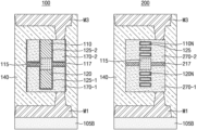
- a stacked semiconductor device 100 includes a 1 st substrate 105 A on which a 1 st active region 110 and a 2 nd active region 120 are stacked in a D3 direction which is perpendicular to a top surface of the substrate 105 A. Between the 1 st active region 110 and the 2 nd active region 120 is formed a 1 st isolation layer 115 which isolates the 2 nd active region from the 1 st active region 110 .
- the 1 st substrate 105 A may be a bulk substrate of a semiconductor material, for example, silicon (Si), silicon germanium (SiGe), a Si-on-insulator, a SiGe-on-insulator, doped or undoped with impurities.
- Each of the 1 st active region 110 and the 2 nd active region 120 may be one or more fin structures which are to form a single or multi-channel of a transistor extended in a D1 direction when completed.
- the fin structures of each of the two active regions 110 and 120 may be a plurality of nanosheet layers to form a nanosheet transistor or a plurality vertical fin structures to form a finFET.
- the D1 direction is a channel length direction perpendicular to a D2 direction which is a channel width direction.
- the 1 st active region 110 and the 2 nd active region 120 may be both epitaxially grown from the 1 st substrate 105 A to have the same crystalline characteristics as the semiconductor material of the 1 st substrate 105 A. According to an embodiment, there may be formed an isolation layer (not shown) between the 1 st active region and the 1 st substrate 105 A to isolate the 1 st active region from the 1 st substrate 105 A.
- the 1 st isolation layer 115 may also be epitaxially grown from the 1 st substrate 105 A except that it includes a different material from the 1 st active region 110 and the 2 nd active region 120 in terms of material concentration, temperature, processing time, etc.
- the isolation layer 115 may include a higher concentration of germanium (Ge) than the two active regions 110 and 120 when each of the two active regions 110 and 120 is formed of a plurality of nanosheet layers.
- germanium germanium
- each of the two active regions 110 and 120 may be grown from respective substrates separately, and bonded to form the stacked structure as shown in FIGS. 1 A to 1 C .
- the 1 st isolation layer 115 may also be separately formed and include a dielectric material such as silicon oxide (SiO) and its equivalent, according to an embodiment.
- FIGS. 1 A and 1 C also show that 1 st source/drain regions 1105 and 110 D (not shown) are formed at both ends of the 1 st active region 110 in a channel length direction, and 2 nd source/drain regions 120 S and 120 D are formed at both ends of the 2 nd active region 120 .
- These source/drain regions may be epitaxially grown from the respective ends of the active regions 110 and 120 in the channel length direction (D1 direction), and insulated from each other by a 2 nd isolation layer 116 which may be formed of the same or similar dielectric material forming the 1 st isolation layer 115 .
- the stacked semiconductor device 100 shown in FIGS. 1 B and 1 C is provided with a dummy gate structure 130 across the 1 st active region 110 and the 2 nd active region 120 .
- the dummy gate structure 130 may be formed on the 1 st substrate 105 A to surround or wrap the two active regions 110 and 120 when viewed in the D1 direction (channel length direction).
- an interlayer dielectric (ILD) layer 140 is formed outside the dummy gate structure 130 as shown in FIG. 2 A .
- This ILD layer 140 may also encompass the 1 st source/drain regions 110 S and 110 D and 2 nd source/drain regions 120 s and 120 D when viewed in the D1 direction.
- the ILD layer 140 may be provide to isolate the stacked semiconductor device 100 from another stacked semiconductor device or circuit element,
- the dummy gate structure 130 may be formed by lithography and etching operations, and may include amorphous silicon, amorphous carbon, diamond-like carbon, dielectric metal oxide, and/or silicon nitride, not being limited thereto.
- the ILD layer 140 may be formed by chemical vapor deposition (CVD) or physical vapor deposition (PVD), not being limited thereto to include an oxide material in bulk (e.g., silicon dioxide having a low- ⁇ dielectric).
- an upper portion of the dummy gate structure 130 surrounding the 1 st active region 110 is removed to form a 1 st void space S 1 in the stacked semiconductor device 100 , for example, by a dry etching, a wet etching, a reactive ion etching (RIE) and/or a chemical oxide removal (COR) process.
- a 3 rd isolation layer 117 is formed at a bottom surface of 1 st void space S 1 which is a top surface of a remaining portion of the dummy gate structure 130 which remains after the upper portion thereof is removed.
- the upper portion of the dummy gate structure 130 is removed such that the 3 rd isolation layer 117 formed on the top surface of the remaining portion of the dummy gate structure 130 is layered at a level corresponding to a vertical middle section of the 1 st isolation layer 115 .
- the 3 rd isolation layer 117 may be layered for isolation of two gate structures which will be formed to surround the two active regions 110 and 120 , respectively, in a later step.
- the 3 rd isolation layer 117 may include the same or similar dielectric material forming the 1 st isolation layer 115 . However, this operation of layering the 3 rd isolation layer 117 is optional, and thus, may be omitted when these two gate structures are to be connected and include the same work function materials to be discussed later.
- a 1 st gate dielectric layer 125 - 1 is conformally formed by, for example, atomic layer deposition (ALD) along an inner surface of the 1 st void space S 1 .
- ALD atomic layer deposition
- the 1 st gate dielectric layer 125 - 1 surrounds the 2 nd active region 120 , and is layered on a top surface of the 3 rd isolation layer 117 , sidewalls of the upper portion of the 1 st isolation layer 115 at a level above the top surface of the 3 rd isolation layer 117 , and sidewalls of an upper portion of the ILD layer 140 at the level above the top surface of the 3 rd isolation layer 117 .
- the 1 st gate dielectric layer 125 - 1 may not be formed on the top surface of the 3 rd isolation layer 117 shown in FIG. 4 B .
- the 1 st gate dielectric layer 125 - 1 may include at least an interfacial layer formed on the 1 st void space S 1 and a high- ⁇ dielectric layer formed on the interfacial layer.
- the interfacial layer may include at least one of SiO, silicon dioxide (SiO 2 ), and/or silicon oxynitride (SiON), not being limited thereto, to protect the 2 nd active region 120 , facilitate growth of the high- ⁇ dielectric layer thereon, and provide a necessary characteristic interface with the 1 st active region 110 .
- the high- ⁇ dielectric layer may be formed of a metal oxide material or a metal silicate such as Hf, Al, Zr, La, Mg, Ba, Ti, Pb, or a combination thereof, not being limited thereto, having a dielectric constant value greater than 7.
- the high- ⁇ dielectric layer may be provided to allow an increased gate capacitance without associated current leakage at a gate structure to be formed later.
- a 1 st replacement polysilicon gate (RPG) structure 150 - 1 is filled in the 1 st void space S 1 in which the 1 st gate dielectric layer 125 - 1 is layered as shown in FIG. 4 B .
- the 1 st RPG structure 150 - 1 takes a shape of surrounding at least the 2 nd active region 120 .
- the 1 st RPG structure 150 - 1 is formed for the purpose of annealing the 1 st gate dielectric layer 125 - 1 to increase reliability of the 1 st gate dielectric layer 125 - 1 in its functions described above.
- this process of RPG structure formation may be optional, and thus, may be omitted, according to an embodiment.
- the 1 st RPG structure 150 - 1 after annealing the 1 st gate dielectric layer 125 - 1 is removed from the 1 st void space S 1 by, for example, a dry etching, wet etching, RIE and/or COR process, and instead, a 1 st replacement metal gate (RMG) structure is filled in the 1 st void space S 1 to form a 1 st gate structure 170 - 1 surrounding at least the 2 nd active region 120 covered by the 1 st gate dielectric layer 125 - 1 .
- RMG replacement metal gate
- the 1 st RMG structure may include a work function metal (WFM) such as Cu, Al, Ti, Ta, W, Co, TiN, WN, TiAl, TiAlN, TaN, TiC, TaC, TiAlC, TaCN, TaSiN, and/or a combination thereof, not being limited thereto.
- WFM work function metal
- a 1 st metal pattern M 1 and a 2 nd metal pattern M 2 may be formed above the 1 st gate structure 170 - 1 and the 2 nd source/drain region 120 S, respectively. Further, a 2 nd substrate 105 B may be formed above these metal pattern M 1 and M 2 . This wafer bonding of the 2 nd substrate may be performed at least to physically support the stacked semiconductor device 100 after the stacked semiconductor device 100 shown in FIGS. 6 A to 6 C is flipped upside down in a next step.
- the 1 st metal pattern M 1 may include a gate contact structure (CB) which may be used to receive and transmit a gate input signal to the 1 st gate structure 170 - 1 .
- the 2 nd metal pattern M 2 may include a source/drain contact structure (CA) which may be used to receive and transmit a power signal to the 2 nd source/drain region 120 S, or output a signal from the 2 nd source/drain region 120 S for internal signal routing.
- CA source/drain contact structure
- an additional ILD layer may be added to extend the ILD layer 140 to surround the 1 st metal pattern M 1 and the 2 nd metal pattern M 2 .
- the stacked semiconductor device 100 shown in FIGS. 6 A to 6 C is flipped upside down, and the 1 st substrate 105 A is removed, for example, by dry etching and/or chemical mechanical planarization (CMP) to expose a remaining portion of the dummy gate structure 130 that is not removed in the step of FIGS. 3 A to 3 C , the ILD layer 140 contacting the 1 st substrate 105 A, and the 1 st source/drain regions 110 S and 110 D (not shown).
- CMP chemical mechanical planarization
- the stacked semiconductor device 100 takes a form of a device formed on the 2 nd substrate 105 B, and the 2 nd active region 120 and the 2 nd source/drain regions 120 S and 120 D are to form a lower-stack transistor of the stacked semiconductor device 100 while the 1 st active region 110 and the 1 st source/drain regions 110 S and 110 D are to form an upper-stack transistor of the stacked semiconductor device 100 in a later step.
- the remaining portion of the dummy gate structure 130 shown in FIGS. 7 A to 7 C is removed to form a 2 nd void space (not shown) in the stacked semiconductor device 100 by a similar method used to remove the upper portion of the dummy gate structure 130 in the step of FIGS. 3 A to 3 C .
- a 2 nd gate dielectric layer 125 - 2 is conformally formed in the 2 nd void space.
- the 2 nd gate dielectric layer 125 - 2 may also not be formed on the top surface of the 3 rd isolation layer 117 shown in FIG. 8 B , according to an embodiment.
- the 2 nd gate dielectric layer 125 - 2 may include the same interfacial layer and the high- ⁇ dielectric layer formed in the 1 st void space S 1 shown in FIG. 4 A to 4 C .
- a 2 nd replacement polysilicon gate (RPG) 150 - 2 structure is formed on the 2 nd gate dielectric layer 125 - 2 to fill in the 2 nd void space for annealing the 2 nd gate dielectric layer 125 - 1 to increase reliability thereof.
- RPG replacement polysilicon gate
- the 2 nd RPG structure 150 - 2 is removed from the 2 nd void space by a similar process used to remove the 1 st RPG structure 150 - 1 in the step of FIGS. 6 A to 6 C , and a 2 nd RMG structure is formed on the 2 nd gate dielectric layer 125 - 2 to fill in the 2 nd void space, thereby forming a 2 nd gate structure 170 - 2 surrounding at least the 1 st active region 110 covered by the 2 nd gate dielectric layer 125 - 2 .
- the 2 nd RMG structure for the 2 nd gate structure 170 - 2 may include a WFM which is the same as or different that of the 1 st RMG structure including Cu, Al, Ti, Ta, W, Co, TiN, WN, TiAl, TiAlN, TaN, TiC, TaC, TiAlC, TaCN, TaSiN, and/or a combination thereof, not being limited thereto.
- the 1 st gate structure 170 - 1 and the 2 nd gate structure 170 - 2 both may be a common gate structure for a lower-stack transistor and an upper-stack transistor of the stacked semiconductor device 100 , both of which may be a p-type or n-type metal oxide semiconductor (PMOS or NMOS).
- PMOS p-type metal oxide semiconductor
- one of the 1 st gate structure 170 - 1 and the 2 nd gate structure 170 - 2 may form one of a PMOS and an NMOS, and the other of the two gate structures 170 - 1 and 170 - 2 may form the other of the PMOS and the NMOS.
- the stacked semiconductor device 100 may take a form of a substantially mirror-symmetric structure in a vertical direction (D3 direction) as seen in FIG. 10 B .
- the 1 st active region 110 and the 2 nd gate structure 170 - 2 may be vertically mirror-symmetric to the 2 nd active region 120 and the 1 st gate structure 170 - 1 , respectively, with respect to a virtual plane therebetween.
- the 3 rd metal pattern M 3 may include a gate contact structure (CB) which may be used to receive and transmit a gate input signal to the 2 nd gate structure 170 - 2 .
- the 4 th metal pattern may include a source/drain contact structure (CA) which may be used to receive and transmit a power signal to the 1 st source/drain region 110 S, or output a signal from the 1 st source/drain region 110 S for internal signal routing.
- CA source/drain contact structure
- FIG. 10 C further shows that a through-silicon via (TSV) is formed to penetrate the stacked semiconductor device 100 , according to an embodiment.
- TSV through-silicon via
- BEOL backend-of-the-line
- an additional ILD layer may be added to extend the ILD layer 140 to surround the 3 rd metal pattern M 3 , the 4 th metal pattern M 4 , and the TSV.
- each of the upper-stack transistor including the 2 nd gate structure 170 - 2 and the lower-stack transistor including the 1 st gate structure 170 - 1 may be a PMOS nanosheet transistor or an NMOS nanosheet transistor.
- the upper-stack transistor and the lower-stack transistor may be a PMOS nanosheet transistor and an NMOS nanosheet transistor, respectively, or vice versa.
- each of the upper-stack transistor and the lower-stack transistor may be a p-type finFET or an n-type finFET.
- the upper-stack transistor and the lower-stack transistor may be a p-type finFET and an n-type finFET, respectively, or vice versa.
- the stacked semiconductor device 100 may be formed to have a substantially mirror-symmetric structure in a vertical direction, in which no middle-of-the-line (MOL) structure is disposed between an upper-stack transistor and a lower-stack transistor.
- MOL middle-of-the-line
- the stacked semiconductor device 100 according to the above embodiment may be able to achieve a substantial area gain compared to the related art stacked semiconductor device which requires an MOL structure between an upper-stack transistor and a lower-stack transistor.
- the mirror-symmetric structure of the stacked semiconductor device may enable easy formation of lateral contact structures, backside metal interconnect structures as well as backside power rails.
- this mirror-symmetric structure of the stacked semiconductor device 100 may apply to a semiconductor device such as a static random access memory (SRAM) and a core which has a repetitive pattern of structure.
- SRAM static random access memory
- FIGS. 11 A to 11 C through 16 A to 16 C illustrate an alternative method of manufacturing a stacked semiconductor device, according to embodiments.
- FIGS. 11 A to 16 A illustrate respective top plan views of a stacked semiconductor device in each step
- FIGS. 16 to 16 B illustrate respective cross-section views of the stacked semiconductor device of FIGS. 16 A to 16 A taken along lines I-I′ thereof, respectively
- FIGS. 16 C to 16 C illustrate respective cross-section views of the stacked semiconductor device of FIGS. 16 A to 16 A taken along a line II-II′ thereof, respectively, according to embodiments.
- the method of this embodiment has the same steps of FIGS. 1 A to 1 C and FIGS. 2 A to 2 C to form a stacked semiconductor device 200 , and thus, duplicate descriptions thereof are omitted, and descriptions directed to only this method begin in reference to FIGS. 11 A to 11 C as below.
- the dummy gate structure 130 surrounding the 1 st active region 110 and the 2 nd active region 120 with the 1 st isolation layer 115 therebetween is entirely removed to form a 3 rd void space S 3 in the stacked semiconductor device 200 , for example, by a dry etching, a wet etching, a reactive ion etching (RIE) and/or a chemical oxide removal (COR) process.
- RIE reactive ion etching
- COR chemical oxide removal
- the dummy gate structure 130 is removed in its entirety to expose the 1 st substrate 105 A in the 3 rd void space S 3 formed in the stacked semiconductor device 200 as shown in FIG. 11 B .
- This difference is intended to enable one time formation of a gate dielectric layer covering both the 1 st active region 110 and the 2 nd active region 120 in a later step to be described below.
- a gate dielectric layer 125 is conformally formed by, for example, ALD along an inner surface of the 3 rd void space S 3 .
- the gate dielectric layer 125 surrounds the stack of the 1 st active region 110 , the 1 st isolation layer 115 and the 2 nd active region 120 , and is layered on a top surface of the 1 st substrate 105 A and sidewalls of the ILD layer 140 exposed by the 3 rd void space S 3 .
- the gate dielectric layer 125 may include the same interfacial layer and high- ⁇ dielectric layer forming the 1 st gate dielectric layer 125 - 1 in the previous embodiment, and thus, the gate dielectric layer 125 may be formed of the same materials forming the 1 st gate dielectric layer 125 - 1 . Accordingly, duplicate descriptions thereof are omitted herein.
- a gate dielectric layer that is, the 1 st gate dielectric layer 125 - 1
- another gate dielectric layer that is, the 2 nd active region 120
- the gate dielectric layer 125 is formed to cover or surround both of the two active regions 110 and 120 by one time process to enable a follow-on step of one-time RPG process for the stacked semiconductor device 200 .
- one time process of forming the gate dielectric layer 125 in the present embodiment enables a more simplified manufacturing process of a stacked semiconductor device.
- an RPG structure 150 is filled in the 3 rd void space S 3 on which the gate dielectric layer 125 is layered as shown in FIG. 12 B .
- the RPG structure 150 is formed for annealing the gate dielectric layer 125 to increase reliability thereof in its functions described above.
- the present embodiment provides one RPG formation process for both of the upper-stack transistor and the lower-stack transistor of the stacked semiconductor device 200 as shown in FIG. 13 B .
- this one time RPG formation process along with one time formation of the gate dielectric layer 125 may be able to address oxide regrowth that may occur in manufacturing of a stacked semiconductor device.
- FIG. 13 B shows that the 1 st active region 110 contacts a top surface of the 1 st substrate 105 A, and thus, the RPG structure 150 does not surround a bottom surface of the 1 st active region 110 , while the RPG structure 150 does surround a top surface of the 2 nd active region 120 .
- the RPG structure 150 may be formed to surround the bottom surface of the 1 st active region 110 , as shown in FIG. 13 D . Referring to FIG.
- the gate dielectric layer 125 is layered on all outer surfaces of a plurality of 1 st nanosheet layers 110 N and a plurality of 2 nd nanosheet layers 120 N, and these nanosheet layers with the gate dielectric layer 125 thereon are surrounded by the RPG structure 150 .
- the gate dielectric layer 125 may not be layered on the top surface of the 1 st substrate 105 and the sidewalls of the ILD layer 140 exposed by the 3 rd void space S 3 in the step of FIGS. 12 A to 12 C .
- an upper portion of the RPG structure 150 shown in FIGS. 13 A and 13 B is removed after annealing the gate dielectric layer 125 .
- This operation of removing the upper portion of the RPG structure 150 may be performed by, for example, a dry etching, a wet etching, a reactive ion etching (RIE) and/or a chemical oxide removal (COR) process.
- RIE reactive ion etching
- COR chemical oxide removal
- the upper portion of the RPG structure 150 is removed such that the 3 rd isolation layer 217 formed on the top surface of the remaining portion of the RPG structure 150 is layered at a level corresponding to a vertical middle portion of the 1st isolation layer 115 .
- the 3 rd isolation layer 217 of the stacked semiconductor device 200 may be formed of the same or similar dielectric material forming the 3 rd isolation layer 117 of the stacked semiconductor device 100 of the previous embodiment as shown in FIGS. 3 A and 3 B . While the 3 rd isolation layer 117 of the stacked semiconductor device 100 is formed above the lower portion of the dummy gate structure 130 and between the 1 st isolation layer 115 and the ILD layer 140 , the 3 rd isolation layer 217 of the stacked semiconductor device 200 is formed above a lower portion (remaining portion) of RPG structure 150 and between the gate dielectric layer 125 formed on the sidewalls of the ILD layer 140 in the 3 rd void space S 3 .
- the 3 rd isolation layer 217 is also formed for isolation of two gate structures to be formed to surround the two active region 110 and 120 , respectively, in a later step, it may not be formed when these two gate structures are to be connected and include the same work function materials, for example for the same PMOS or NMOS.
- a 1 st RMG structure for a 1 st gate structure 270 - 1 is formed on the 3 rd isolation layer 217 so that the 1 st RMG and the 3 rd isolation layer 217 replaces the removed upper portion of the RPG structure 150 in the 3 rd void space S 3 of the stacked semiconductor device 200 .
- the 1 st RMG structure for the 1 st gate structure 270 - 1 may be formed of the same material as the 1 st RMG structure for the 1 st gate structure 170 - 1 of the stacked semiconductor device 100 of the previous embodiment shown in FIG. 6 B , and thus, descriptions thereof are omitted.
- the same 1 st metal pattern M 1 , 2 nd metal pattern M 2 , and 2 nd substrate 105 B shown in FIGS. 6 A and 6 B may be patterned above the 1 st gate structure 270 - 1 and the 2 nd source/drain region 120 S, respectively, for the same purpose described above, as shown in FIGS. 14 A and 14 B .
- an additional ILD layer may be added to extend the ILD layer 140 to surround the 1 st metal pattern M 1 and the 2 nd metal pattern M 2 .
- the stacked semiconductor device 200 shown in FIG. 14 B may take the structure shown in FIG. 14 D , according to an embodiment.
- the stacked semiconductor device 200 shown in FIGS. 14 A to 14 C is flipped upside down, and the 1 st substrate 105 A is removed, for example, by dry etching to expose the remaining portion of the RPG structure 150 , that is not removed in the step of FIGS. 14 A to 14 C , the ILD layer 140 contacting the 1 st substrate 105 A, and the 1 st source/drain regions 110 S and 110 D (not shown).
- the stacked semiconductor device 200 also takes a form of a device formed on the 2 nd substrate 105 B, and the 2 nd active region 120 and the 2 nd source/drain regions 120 S and 120 D are to form a lower-stack transistor of the stacked semiconductor device 100 while the 1 st active region 110 and the 1 st source/drain regions 110 S and 110 D are to form an upper-stack transistor of the stacked semiconductor device 200 in a later step.
- the stacked semiconductor device 200 shown in FIG. 15 B may take the structure shown in FIG. 15 D , according to an embodiment.
- the remaining portion of the RPG structure 150 is removed by the same process used to remove the upper portion of the RPG structure 150 in the step of FIGS. 14 A to 14 C , and a 2 nd RMG structure is formed on the 3 rd isolation layer 217 and between the gate dielectric layer 125 , thereby forming a 2 nd gate structure 270 - 2 .
- the 2 nd RMG structure for the 2 nd gate structure 270 - 2 may include the same or different WFM such as from the 1 st RMG structure among Cu, Al, Ti, Ta, W, Co, TiN, WN, TiAl, TiAlN, TaN, TiC, TaC, TiAlC, TaCN, TaSiN, and/or a combination thereof, not being limited thereto.
- the 1 st RMC structure and the 2 nd RMG structure are formed of the same WFM
- the 1 st gate structure 270 - 1 and the 2 nd gate structure 270 - 2 both may be a common gate structure for a p-type or n-type metal oxide semiconductor (PMOS or NMOS).
- one of the 1 st gate structure 270 - 1 and the 2 nd gate structure 270 - 2 may form one of a PMOS and an NMOS, and the other of the two gate structures 270 - 1 and 270 - 2 may form the other of the PMOS and the NMOS.
- the same 3 rd metal pattern M 3 and 4 th metal pattern M 4 and TSV shown in FIGS. 10 A and 10 B may be formed as shown in FIGS. 16 A and 16 B for the same purpose.
- the stacked semiconductor device 200 may take a form of a substantially mirror-symmetric structure in the vertical direction (D3 direction) as seen in FIG. 16 B .
- the 1 st active region 110 and the 2 nd gate structure 270 - 2 may be vertically mirror-symmetric to the 2 nd active region 120 and the 1 st gate structure 270 - 1 , respectively, with respect to a virtual plane therebetween.
- an additional ILD layer may be added to extend the ILD layer 140 to surround the 3 rd metal pattern M 3 and 4 th metal pattern M 4 and TSV.
- the stacked semiconductor device 200 shown in FIG. 15 B may take the structure shown in FIG. 16 D , according to an embodiment.
- each of the upper-stack transistor including the 2 nd gate structure 270 - 2 and the lower-stack transistor including the 1 st gate structure 270 - 1 may be a PMOS nanosheet transistor or an NMOS nanosheet transistor.
- the upper-stack transistor and the lower-stack transistor may be a PMOS nanosheet transistor and an NMOS nanosheet transistor, respectively, or vice versa.
- each of the upper-stack transistor and the lower-stack transistor may be a p-type finFET or an n-type finFET.
- the upper-stack transistor and the lower-stack transistor may be a p-type finFET and an n-type finFET, respectively, or vice versa.
- FIG. 17 illustrates a flowchart of forming a stacked semiconductor device in reference to FIGS. 1 A to 1 C through 10 A to 10 C , according to an embodiment.
- a 1 st active region, a 1 st isolation layer, and a 2 nd active region are stacked on a 1 st substrate, and 1 st source/drain regions, a 2 nd isolation layer, and 2 nd source/drain regions are formed at both ends of the 1 st active region, the 1 st isolation layer, and the 2 nd active region, respectively, to form a stacked semiconductor device, as shown in FIGS. 1 A to 1 C .
- a dummy gate structure is formed to cover the 1 st active region, the 1 st isolation layer, and the 2 nd active region, as shown in FIGS. 2 A to 2 C .
- an upper portion of the dummy gate structure is removed to form a 1 st void space having a bottom surface as a top surface of a remaining portion of the dummy gate structure, and a 3 rd isolation layer may be optionally layered on a top surface of a remaining portion of the dummy gate structure to have a vertical location corresponding to a vertical middle section of the 2 nd isolation layer, as shown in FIGS. 3 A to 3 C .
- a 1 st gate dielectric layer is conformally layered in the 1 st void space, where the 2 nd isolation layer is layered at the bottom thereof, to surround at least the 2 nd active region, as shown in FIGS. 4 A to 4 C .
- a 1 st RPG structure is filled in the 1 st void space for annealing the 1 st gate dielectric layer layered in the 1 st void space, as shown in FIGS. 5 A to 5 C .
- this process of RPG structure formation may be optional, and thus, may be omitted, according to an embodiment.
- the 1 st RPG structure after annealing the 1 st gate dielectric layer is replaced with a 1 st RMG structure to form a 1 st gate structure of the stacked semiconductor device, followed by forming a 1 st metal pattern, a 2 nd metal pattern above the 1 st gate structure and the 2 nd source/drain region for respective connections thereto, and forming a 2 nd substrate on the 1 st metal pattern and the 2 nd metal pattern, as shown in FIGS. 6 A to 6 C .
- the stacked semiconductor device is flipped upside down and the 1 st substrate is removed, by which the 2 nd substrate supports the stacked semiconductor device, and the 1 st active region and the 1 st source/drain regions are disposed above the 2 nd active region and the 2 nd source/drain regions with the 1 st isolation layer and the 2 nd isolation layer therebetween, respectively, as shown in FIGS. 7 A to 7 C .
- the remaining portion of the dummy gate structure is removed to form a 2 nd void space, following by forming the 2 nd gate dielectric layer and the 2 nd RPG structure in the 2 nd void space, as shown in FIGS. 8 A to 8 C .
- the 2 nd RPG structure is removed from the 2 nd void space and a 2 nd RMG structure is formed on the 2 nd gate dielectric layer in the 2 nd void space to form a 2 nd gate structure, thereby the 2 nd gate structure along with the 1 st source/drain regions forming an upper-stack transistor, and the 1 st gate structure along with the 2 nd source/drain regions forming a lower-stack transistor of the stacked semiconductor device, as shown in FIGS. 9 A to 9 C .
- a 3 rd metal pattern and a 4 th metal pattern are formed above the 2 nd gate structure and the 1 st source/drain region for respective connections thereto, and a BEOL structure such as TSV is formed to penetrate the stacked semiconductor device so that the upper-stack transistor and the lower-stack transistor can be electrically connected to each other, as shown in FIGS. 10 A to 10 C .
- FIG. 18 illustrates a flowchart of forming a stacked semiconductor device in reference to FIGS. 1 A to 1 C, 2 A to 2 C and 11 A to 11 C through 16 A to 16 C , according to an embodiment.
- a 1 st active region, a 1 st isolation layer, and a 2 nd active region are stacked on a 1 st substrate, and 1 st source/drain regions, a 2 nd isolation layer, and 2 nd source/drain regions are formed at both ends of the 1 st active region, the 1 st isolation layer, and the 2 nd active region, respectively, to form a stacked semiconductor device as shown in FIGS. 1 A to 1 C .
- a dummy gate structure is formed to cover the 1 st active region, the 1 st isolation layer, and the 2 nd active region, as shown in FIGS. 2 A to 2 C .
- the dummy gate structure surrounding the 1 st active region and the 2 nd active region with the 1 st isolation layer therebetween is entirely removed to form a void space (the 3 rd void space S 3 in FIG. 11 B ) in the stacked semiconductor device, as shown in FIGS. 11 A to 11 C .
- a gate dielectric layer is conformally layered in the void space to surround the 1 st active region, the 1 st isolation layer and the 2 nd active region, as shown in FIGS. 12 A to 12 C .
- an RPG structure is filled in the void space on which the gate dielectric layer is layered, as shown in FIGS. 13 A to 13 C .
- an upper portion of the RPG structure is removed, a 3 rd isolation layer is formed on a top surface of the remaining RPG structure in the void space S 3 , and a 1 st RMG structure for a 1 st gate structure is formed on the 3 rd isolation layer 217 in the void space, followed by forming a 1 st metal pattern, a 2 nd metal pattern above the 1 st gate structure and the 2 nd source/drain region for respective connections thereto, and forming a 2 nd substrate on the 1 st metal pattern and the 2 nd metal pattern, as shown in FIGS. 14 A to 14 C .
- this process of RPG structure formation may be optional.
- the stacked semiconductor device is flipped upside down and the 1 st substrate is removed, by which the 2 nd substrate supports the stacked semiconductor device, and the 1 st active region and the 1 st source/drain regions are disposed above the 2 nd active region and the 2 nd source/drain regions with the 1 st isolation layer and the 2 nd isolation layer therebetween, respectively, as shown in FIGS. 15 A to 15 C .
- the remaining portion of the RPG structure is replaced with a 2 nd RMG structure to form a 2 nd gate structure, thereby the 2 nd gate structure along with the 1 st source/drain regions forming an upper-stack transistor, and the 1 st gate structure along with the 2 nd source/drain regions forming a lower-stack transistor of the stacked semiconductor device, as shown in FIGS. 16 A to 16 C .
- a 3 rd metal pattern and a 4 th metal pattern are formed above the 2 nd gate structure and the 1 st source/drain region for respective connections thereto, and a BEOL structure such as TSV is formed to penetrate the stacked semiconductor device so that the upper-stack transistor and the lower-stack transistor can be electrically connected to each other, as also shown in FIGS. 16 A to 16 C .
- FIG. 19 illustrates a schematic plan view of a semiconductor module according to an embodiment.
- a semiconductor module 600 may include a processor 620 and semiconductor devices 630 that are mounted on a module substrate 610 .
- the processor 620 and/or the semiconductor devices 630 may include one or more multi-stack nanosheet structures described in the above embodiments.
- FIG. 20 illustrates a schematic block diagram of an electronic system according to an embodiment.
- an electronic system 700 in accordance with an embodiment may include a microprocessor 710 , a memory 720 , and a user interface 730 that perform data communication using a bus 740 .
- the microprocessor 710 may include a central processing unit (CPU) or an application processor (AP).
- the electronic system 700 may further include a random access memory (RAM) 750 in direct communication with the microprocessor 710 .
- the microprocessor 710 and/or the RAM 750 may be implemented in a single module or package.
- the user interface 730 may be used to input data to the electronic system 700 , or output data from the electronic system 700 .
- the user interface 730 may include a keyboard, a touch pad, a touch screen, a mouse, a scanner, a voice detector, a liquid crystal display (LCD), a micro light-emitting device (LED), an organic light-emitting diode (OLED) device, an active-matrix light-emitting diode (AMOLED) device, a printer, a lighting, or various other input/output devices without limitation.
- the memory 720 may store operational codes of the microprocessor 710 , data processed by the microprocessor 710 , or data received from an external device.
- the memory 720 may include a memory controller, a hard disk, or a solid state drive (SSD).
- At least the microprocessor 710 , the memory 720 and/or the RAM 750 in the electronic system 700 may include one or more stacked semiconductor device described in the above embodiments.
Abstract
Description
Claims (16)
Priority Applications (6)
| Application Number | Priority Date | Filing Date | Title |
|---|---|---|---|
| US17/223,829 US11735585B2 (en) | 2021-01-18 | 2021-04-06 | Stacked semiconductor device having mirror-symmetric pattern |
| KR1020210108654A KR20220105575A (en) | 2021-01-18 | 2021-08-18 | Stacked semiconductor device having mirror-symmetric pattern |
| EP21199064.3A EP4030470A1 (en) | 2021-01-18 | 2021-09-27 | Stacked semiconductor device having mirror-symmetric pattern |
| TW110136745A TW202232756A (en) | 2021-01-18 | 2021-10-01 | Stacked semiconductor device having mirror-symmetric pattern and method for manufacturing the same |
| CN202111570992.8A CN114823666A (en) | 2021-01-18 | 2021-12-21 | Stacked semiconductor device and method of manufacturing the same |
| US18/356,545 US20230369317A1 (en) | 2021-01-18 | 2023-07-21 | Stacked semiconductor device having mirror-symmetric pattern |
Applications Claiming Priority (2)
| Application Number | Priority Date | Filing Date | Title |
|---|---|---|---|
| US202163138594P | 2021-01-18 | 2021-01-18 | |
| US17/223,829 US11735585B2 (en) | 2021-01-18 | 2021-04-06 | Stacked semiconductor device having mirror-symmetric pattern |
Related Child Applications (1)
| Application Number | Title | Priority Date | Filing Date |
|---|---|---|---|
| US18/356,545 Continuation US20230369317A1 (en) | 2021-01-18 | 2023-07-21 | Stacked semiconductor device having mirror-symmetric pattern |
Publications (2)
| Publication Number | Publication Date |
|---|---|
| US20220231013A1 US20220231013A1 (en) | 2022-07-21 |
| US11735585B2 true US11735585B2 (en) | 2023-08-22 |
Family
ID=77989747
Family Applications (2)
| Application Number | Title | Priority Date | Filing Date |
|---|---|---|---|
| US17/223,829 Active 2041-04-27 US11735585B2 (en) | 2021-01-18 | 2021-04-06 | Stacked semiconductor device having mirror-symmetric pattern |
| US18/356,545 Pending US20230369317A1 (en) | 2021-01-18 | 2023-07-21 | Stacked semiconductor device having mirror-symmetric pattern |
Family Applications After (1)
| Application Number | Title | Priority Date | Filing Date |
|---|---|---|---|
| US18/356,545 Pending US20230369317A1 (en) | 2021-01-18 | 2023-07-21 | Stacked semiconductor device having mirror-symmetric pattern |
Country Status (5)
| Country | Link |
|---|---|
| US (2) | US11735585B2 (en) |
| EP (1) | EP4030470A1 (en) |
| KR (1) | KR20220105575A (en) |
| CN (1) | CN114823666A (en) |
| TW (1) | TW202232756A (en) |
Families Citing this family (2)
| Publication number | Priority date | Publication date | Assignee | Title |
|---|---|---|---|---|
| US20220320084A1 (en) * | 2021-03-31 | 2022-10-06 | Taiwan Semiconductor Manufacturing Company, Ltd. | Integrated circuit structure and manufacturing method thereof |
| US20240071926A1 (en) * | 2022-08-31 | 2024-02-29 | International Business Machines Corporation | Transistors with dual power and signal lines |
Citations (19)
| Publication number | Priority date | Publication date | Assignee | Title |
|---|---|---|---|---|
| US20160043108A1 (en) | 2014-08-07 | 2016-02-11 | Silanna Semiconductor U.S.A., Inc. | Semiconductor Structure with Multiple Active Layers in an SOI Wafer |
| WO2016204755A1 (en) | 2015-06-17 | 2016-12-22 | Intel Corporation | Vertical integration scheme and circuit elements architecture for area scaling of semiconductor devices |
| US9613844B2 (en) * | 2010-11-18 | 2017-04-04 | Monolithic 3D Inc. | 3D semiconductor device having two layers of transistors |
| US9627270B2 (en) * | 2015-05-11 | 2017-04-18 | International Business Machines Corporation | Dual work function integration for stacked FinFET |
| US9837414B1 (en) | 2016-10-31 | 2017-12-05 | International Business Machines Corporation | Stacked complementary FETs featuring vertically stacked horizontal nanowires |
| US20180315838A1 (en) * | 2015-12-18 | 2018-11-01 | Intel Corporation | Stacked transistors |
| US10236292B1 (en) | 2018-02-05 | 2019-03-19 | Globalfoundries Inc. | Complementary FETs with wrap around contacts and methods of forming same |
| US10420171B2 (en) | 2016-08-26 | 2019-09-17 | Qualcomm Incorporated | Semiconductor devices on two sides of an isolation layer |
| US20190319095A1 (en) * | 2017-11-02 | 2019-10-17 | International Business Machines Corporation | Vertically stacked nfets and pfets with gate-all-around structure |
| US20190326175A1 (en) * | 2017-03-30 | 2019-10-24 | Intel Corporation | Vertically stacked transistors in a pin |
| US20200105751A1 (en) * | 2018-09-28 | 2020-04-02 | Intel Corporation | Stacked transistor architecture including nanowire or nanoribbon thin film transistors |
| US20200118891A1 (en) | 2018-10-10 | 2020-04-16 | International Business Machines Corporation | Vertically stacked nanosheet cmos transistor |
| US20200119015A1 (en) | 2018-10-12 | 2020-04-16 | International Business Machines Corporation | Stacked nanosheet complementary metal oxide semiconductor field effect transistor devices |
| EP3675158A2 (en) | 2018-12-28 | 2020-07-01 | Intel Corporation | Three dimensional integrated circuits with stacked transistors |
| US20200219979A1 (en) | 2019-01-04 | 2020-07-09 | Intel Corporation | Gate-all-around integrated circuit structures having depopulated channel structures using bottom-up oxidation approach |
| US20200403034A1 (en) * | 2019-06-19 | 2020-12-24 | International Business Machines Corporation | Stacked resistive memory with individual switch control |
| US20210035975A1 (en) * | 2019-08-02 | 2021-02-04 | Samsung Electronics Co., Ltd. | Semiconductor devices |
| US20210391207A1 (en) * | 2020-06-11 | 2021-12-16 | Tokyo Electron Limited | Method of making 3d isolation |
| US20210407999A1 (en) * | 2020-06-26 | 2021-12-30 | Intel Corporation | Stacked forksheet transistors |
-
2021
- 2021-04-06 US US17/223,829 patent/US11735585B2/en active Active
- 2021-08-18 KR KR1020210108654A patent/KR20220105575A/en unknown
- 2021-09-27 EP EP21199064.3A patent/EP4030470A1/en active Pending
- 2021-10-01 TW TW110136745A patent/TW202232756A/en unknown
- 2021-12-21 CN CN202111570992.8A patent/CN114823666A/en active Pending
-
2023
- 2023-07-21 US US18/356,545 patent/US20230369317A1/en active Pending
Patent Citations (19)
| Publication number | Priority date | Publication date | Assignee | Title |
|---|---|---|---|---|
| US9613844B2 (en) * | 2010-11-18 | 2017-04-04 | Monolithic 3D Inc. | 3D semiconductor device having two layers of transistors |
| US20160043108A1 (en) | 2014-08-07 | 2016-02-11 | Silanna Semiconductor U.S.A., Inc. | Semiconductor Structure with Multiple Active Layers in an SOI Wafer |
| US9627270B2 (en) * | 2015-05-11 | 2017-04-18 | International Business Machines Corporation | Dual work function integration for stacked FinFET |
| WO2016204755A1 (en) | 2015-06-17 | 2016-12-22 | Intel Corporation | Vertical integration scheme and circuit elements architecture for area scaling of semiconductor devices |
| US20180315838A1 (en) * | 2015-12-18 | 2018-11-01 | Intel Corporation | Stacked transistors |
| US10420171B2 (en) | 2016-08-26 | 2019-09-17 | Qualcomm Incorporated | Semiconductor devices on two sides of an isolation layer |
| US9837414B1 (en) | 2016-10-31 | 2017-12-05 | International Business Machines Corporation | Stacked complementary FETs featuring vertically stacked horizontal nanowires |
| US20190326175A1 (en) * | 2017-03-30 | 2019-10-24 | Intel Corporation | Vertically stacked transistors in a pin |
| US20190319095A1 (en) * | 2017-11-02 | 2019-10-17 | International Business Machines Corporation | Vertically stacked nfets and pfets with gate-all-around structure |
| US10236292B1 (en) | 2018-02-05 | 2019-03-19 | Globalfoundries Inc. | Complementary FETs with wrap around contacts and methods of forming same |
| US20200105751A1 (en) * | 2018-09-28 | 2020-04-02 | Intel Corporation | Stacked transistor architecture including nanowire or nanoribbon thin film transistors |
| US20200118891A1 (en) | 2018-10-10 | 2020-04-16 | International Business Machines Corporation | Vertically stacked nanosheet cmos transistor |
| US20200119015A1 (en) | 2018-10-12 | 2020-04-16 | International Business Machines Corporation | Stacked nanosheet complementary metal oxide semiconductor field effect transistor devices |
| EP3675158A2 (en) | 2018-12-28 | 2020-07-01 | Intel Corporation | Three dimensional integrated circuits with stacked transistors |
| US20200219979A1 (en) | 2019-01-04 | 2020-07-09 | Intel Corporation | Gate-all-around integrated circuit structures having depopulated channel structures using bottom-up oxidation approach |
| US20200403034A1 (en) * | 2019-06-19 | 2020-12-24 | International Business Machines Corporation | Stacked resistive memory with individual switch control |
| US20210035975A1 (en) * | 2019-08-02 | 2021-02-04 | Samsung Electronics Co., Ltd. | Semiconductor devices |
| US20210391207A1 (en) * | 2020-06-11 | 2021-12-16 | Tokyo Electron Limited | Method of making 3d isolation |
| US20210407999A1 (en) * | 2020-06-26 | 2021-12-30 | Intel Corporation | Stacked forksheet transistors |
Non-Patent Citations (1)
| Title |
|---|
| Communication dated Mar. 1, 2022 issued by the European Patent Office in application No. 21199064.3. |
Also Published As
| Publication number | Publication date |
|---|---|
| US20220231013A1 (en) | 2022-07-21 |
| CN114823666A (en) | 2022-07-29 |
| TW202232756A (en) | 2022-08-16 |
| KR20220105575A (en) | 2022-07-27 |
| US20230369317A1 (en) | 2023-11-16 |
| EP4030470A1 (en) | 2022-07-20 |
Similar Documents
| Publication | Publication Date | Title |
|---|---|---|
| US10692879B2 (en) | Semiconductor device including different orientations of memory cell array and peripheral circuit transistors | |
| US20230369317A1 (en) | Stacked semiconductor device having mirror-symmetric pattern | |
| US10325909B2 (en) | ROM chip manufacturing structures having shared gate electrodes | |
| TWI466293B (en) | Integrated circuit having metal gate stacks and method for manufacturing the same | |
| US20230231015A1 (en) | Crossing multi-stack nanosheet structure and method of manufacturing the same | |
| US20170062420A1 (en) | Semiconductor device | |
| JP2004165197A (en) | Semiconductor integrated circuit device and method of manufacturing the same | |
| CN115884590A (en) | Semiconductor device with a plurality of semiconductor chips | |
| US20220336473A1 (en) | Selective double diffusion break structures for multi-stack semiconductor device | |
| CN116097914A (en) | Memory device with vertical transistor and method of forming the same | |
| US11355640B1 (en) | Hybrid multi-stack semiconductor device including self-aligned channel structure and method of manufacturing the same | |
| US11901240B2 (en) | Multi-fin vertical field effect transistor and single-fin vertical field effect transistor on a single integrated circuit chip | |
| US11569232B2 (en) | Semiconductor device including self-aligned gate structure and method of manufacturing the same | |
| US20240136288A1 (en) | Hybrid Power Rail Formation in Dielectric Isolation for Semiconductor Device | |
| US20220139900A1 (en) | Semiconductor device | |
| US20230377983A1 (en) | Method to reduce parasitic resistance for cfet devices through single damascene processing of vias | |
| US20230377985A1 (en) | Method for wrap-around contact formation through the incorporation of cladding of an etch-selective semiconductor material | |
| US20230377998A1 (en) | Method of forming confined growth s/d contact with selective deposition of inner spacer for cfet | |
| US20210375940A1 (en) | Three-dimensional memory device and methods of forming | |
| US20220020774A1 (en) | Memory device and method for fabricating the same | |
| WO2023225155A1 (en) | Sequential complimentary fet incorporating backside power distribution network through wafer bonding prior to formation of active devices | |
| KR20230145911A (en) | Vertical pn connection in multi-stack semiconductor |
Legal Events
| Date | Code | Title | Description |
|---|---|---|---|
| AS | Assignment |
Owner name: SAMSUNG ELECTRONICS CO., LTD., KOREA, REPUBLIC OF Free format text: ASSIGNMENT OF ASSIGNORS INTEREST;ASSIGNORS:HONG, BYOUNGHAK;SONG, SEUNGHYUN;SIGNING DATES FROM 20210401 TO 20210403;REEL/FRAME:055841/0672 |
|
| FEPP | Fee payment procedure |
Free format text: ENTITY STATUS SET TO UNDISCOUNTED (ORIGINAL EVENT CODE: BIG.); ENTITY STATUS OF PATENT OWNER: LARGE ENTITY |
|
| AS | Assignment |
Owner name: SAMSUNG ELECTRONICS CO., LTD., KOREA, REPUBLIC OF Free format text: CORRECTIVE ASSIGNMENT TO CORRECT THE CONVEYING PARTY DATA BY OMISSION THE INVENTOR NAMES PREVIOUSLY RECORDED AT REEL: 055841 FRAME: 0672. ASSIGNOR(S) HEREBY CONFIRMS THE ASSIGNMENT OF ASSIGNOR'S INTEREST;ASSIGNORS:HONG, BYOUNGHAK;SONG, SEUNGHYUN;JUN, HWICHAN;AND OTHERS;SIGNING DATES FROM 20210401 TO 20210413;REEL/FRAME:055942/0062 |
|
| STPP | Information on status: patent application and granting procedure in general |
Free format text: RESPONSE TO NON-FINAL OFFICE ACTION ENTERED AND FORWARDED TO EXAMINER |
|
| STPP | Information on status: patent application and granting procedure in general |
Free format text: NON FINAL ACTION MAILED |
|
| STPP | Information on status: patent application and granting procedure in general |
Free format text: RESPONSE TO NON-FINAL OFFICE ACTION ENTERED AND FORWARDED TO EXAMINER |
|
| STPP | Information on status: patent application and granting procedure in general |
Free format text: PUBLICATIONS -- ISSUE FEE PAYMENT VERIFIED |
|
| STCF | Information on status: patent grant |
Free format text: PATENTED CASE |