EP1851797B1 - Device and method for fabricating double-sided soi wafer scale package with through via connections - Google Patents
Device and method for fabricating double-sided soi wafer scale package with through via connections Download PDFInfo
- Publication number
- EP1851797B1 EP1851797B1 EP05807945A EP05807945A EP1851797B1 EP 1851797 B1 EP1851797 B1 EP 1851797B1 EP 05807945 A EP05807945 A EP 05807945A EP 05807945 A EP05807945 A EP 05807945A EP 1851797 B1 EP1851797 B1 EP 1851797B1
- Authority
- EP
- European Patent Office
- Prior art keywords
- wafer
- chip
- chips
- cavity
- recited
- Prior art date
- Legal status (The legal status is an assumption and is not a legal conclusion. Google has not performed a legal analysis and makes no representation as to the accuracy of the status listed.)
- Not-in-force
Links
Images


Classifications
-
- H—ELECTRICITY
- H01—ELECTRIC ELEMENTS
- H01L—SEMICONDUCTOR DEVICES NOT COVERED BY CLASS H10
- H01L21/00—Processes or apparatus adapted for the manufacture or treatment of semiconductor or solid state devices or of parts thereof
- H01L21/70—Manufacture or treatment of devices consisting of a plurality of solid state components formed in or on a common substrate or of parts thereof; Manufacture of integrated circuit devices or of parts thereof
- H01L21/71—Manufacture of specific parts of devices defined in group H01L21/70
- H01L21/768—Applying interconnections to be used for carrying current between separate components within a device comprising conductors and dielectrics
- H01L21/76898—Applying interconnections to be used for carrying current between separate components within a device comprising conductors and dielectrics formed through a semiconductor substrate
-
- H—ELECTRICITY
- H01—ELECTRIC ELEMENTS
- H01L—SEMICONDUCTOR DEVICES NOT COVERED BY CLASS H10
- H01L23/00—Details of semiconductor or other solid state devices
- H01L23/48—Arrangements for conducting electric current to or from the solid state body in operation, e.g. leads, terminal arrangements ; Selection of materials therefor
- H01L23/481—Internal lead connections, e.g. via connections, feedthrough structures
-
- H—ELECTRICITY
- H01—ELECTRIC ELEMENTS
- H01L—SEMICONDUCTOR DEVICES NOT COVERED BY CLASS H10
- H01L24/00—Arrangements for connecting or disconnecting semiconductor or solid-state bodies; Methods or apparatus related thereto
- H01L24/01—Means for bonding being attached to, or being formed on, the surface to be connected, e.g. chip-to-package, die-attach, "first-level" interconnects; Manufacturing methods related thereto
- H01L24/02—Bonding areas ; Manufacturing methods related thereto
- H01L24/04—Structure, shape, material or disposition of the bonding areas prior to the connecting process
- H01L24/05—Structure, shape, material or disposition of the bonding areas prior to the connecting process of an individual bonding area
-
- H—ELECTRICITY
- H01—ELECTRIC ELEMENTS
- H01L—SEMICONDUCTOR DEVICES NOT COVERED BY CLASS H10
- H01L24/00—Arrangements for connecting or disconnecting semiconductor or solid-state bodies; Methods or apparatus related thereto
- H01L24/93—Batch processes
- H01L24/94—Batch processes at wafer-level, i.e. with connecting carried out on a wafer comprising a plurality of undiced individual devices
-
- H—ELECTRICITY
- H01—ELECTRIC ELEMENTS
- H01L—SEMICONDUCTOR DEVICES NOT COVERED BY CLASS H10
- H01L25/00—Assemblies consisting of a plurality of individual semiconductor or other solid state devices ; Multistep manufacturing processes thereof
- H01L25/03—Assemblies consisting of a plurality of individual semiconductor or other solid state devices ; Multistep manufacturing processes thereof all the devices being of a type provided for in the same subgroup of groups H01L27/00 - H01L33/00, or in a single subclass of H10K, H10N, e.g. assemblies of rectifier diodes
- H01L25/04—Assemblies consisting of a plurality of individual semiconductor or other solid state devices ; Multistep manufacturing processes thereof all the devices being of a type provided for in the same subgroup of groups H01L27/00 - H01L33/00, or in a single subclass of H10K, H10N, e.g. assemblies of rectifier diodes the devices not having separate containers
- H01L25/065—Assemblies consisting of a plurality of individual semiconductor or other solid state devices ; Multistep manufacturing processes thereof all the devices being of a type provided for in the same subgroup of groups H01L27/00 - H01L33/00, or in a single subclass of H10K, H10N, e.g. assemblies of rectifier diodes the devices not having separate containers the devices being of a type provided for in group H01L27/00
- H01L25/0652—Assemblies consisting of a plurality of individual semiconductor or other solid state devices ; Multistep manufacturing processes thereof all the devices being of a type provided for in the same subgroup of groups H01L27/00 - H01L33/00, or in a single subclass of H10K, H10N, e.g. assemblies of rectifier diodes the devices not having separate containers the devices being of a type provided for in group H01L27/00 the devices being arranged next and on each other, i.e. mixed assemblies
-
- H—ELECTRICITY
- H01—ELECTRIC ELEMENTS
- H01L—SEMICONDUCTOR DEVICES NOT COVERED BY CLASS H10
- H01L25/00—Assemblies consisting of a plurality of individual semiconductor or other solid state devices ; Multistep manufacturing processes thereof
- H01L25/18—Assemblies consisting of a plurality of individual semiconductor or other solid state devices ; Multistep manufacturing processes thereof the devices being of types provided for in two or more different subgroups of the same main group of groups H01L27/00 - H01L33/00, or in a single subclass of H10K, H10N
-
- H—ELECTRICITY
- H01—ELECTRIC ELEMENTS
- H01L—SEMICONDUCTOR DEVICES NOT COVERED BY CLASS H10
- H01L2221/00—Processes or apparatus adapted for the manufacture or treatment of semiconductor or solid state devices or of parts thereof covered by H01L21/00
- H01L2221/67—Apparatus for handling semiconductor or electric solid state devices during manufacture or treatment thereof; Apparatus for handling wafers during manufacture or treatment of semiconductor or electric solid state devices or components; Apparatus not specifically provided for elsewhere
- H01L2221/683—Apparatus for handling semiconductor or electric solid state devices during manufacture or treatment thereof; Apparatus for handling wafers during manufacture or treatment of semiconductor or electric solid state devices or components; Apparatus not specifically provided for elsewhere for supporting or gripping
- H01L2221/68304—Apparatus for handling semiconductor or electric solid state devices during manufacture or treatment thereof; Apparatus for handling wafers during manufacture or treatment of semiconductor or electric solid state devices or components; Apparatus not specifically provided for elsewhere for supporting or gripping using temporarily an auxiliary support
- H01L2221/68345—Apparatus for handling semiconductor or electric solid state devices during manufacture or treatment thereof; Apparatus for handling wafers during manufacture or treatment of semiconductor or electric solid state devices or components; Apparatus not specifically provided for elsewhere for supporting or gripping using temporarily an auxiliary support used as a support during the manufacture of self supporting substrates
-
- H—ELECTRICITY
- H01—ELECTRIC ELEMENTS
- H01L—SEMICONDUCTOR DEVICES NOT COVERED BY CLASS H10
- H01L2221/00—Processes or apparatus adapted for the manufacture or treatment of semiconductor or solid state devices or of parts thereof covered by H01L21/00
- H01L2221/67—Apparatus for handling semiconductor or electric solid state devices during manufacture or treatment thereof; Apparatus for handling wafers during manufacture or treatment of semiconductor or electric solid state devices or components; Apparatus not specifically provided for elsewhere
- H01L2221/683—Apparatus for handling semiconductor or electric solid state devices during manufacture or treatment thereof; Apparatus for handling wafers during manufacture or treatment of semiconductor or electric solid state devices or components; Apparatus not specifically provided for elsewhere for supporting or gripping
- H01L2221/68304—Apparatus for handling semiconductor or electric solid state devices during manufacture or treatment thereof; Apparatus for handling wafers during manufacture or treatment of semiconductor or electric solid state devices or components; Apparatus not specifically provided for elsewhere for supporting or gripping using temporarily an auxiliary support
- H01L2221/68363—Apparatus for handling semiconductor or electric solid state devices during manufacture or treatment thereof; Apparatus for handling wafers during manufacture or treatment of semiconductor or electric solid state devices or components; Apparatus not specifically provided for elsewhere for supporting or gripping using temporarily an auxiliary support used in a transfer process involving transfer directly from an origin substrate to a target substrate without use of an intermediate handle substrate
-
- H—ELECTRICITY
- H01—ELECTRIC ELEMENTS
- H01L—SEMICONDUCTOR DEVICES NOT COVERED BY CLASS H10
- H01L2224/00—Indexing scheme for arrangements for connecting or disconnecting semiconductor or solid-state bodies and methods related thereto as covered by H01L24/00
- H01L2224/01—Means for bonding being attached to, or being formed on, the surface to be connected, e.g. chip-to-package, die-attach, "first-level" interconnects; Manufacturing methods related thereto
- H01L2224/02—Bonding areas; Manufacturing methods related thereto
- H01L2224/04—Structure, shape, material or disposition of the bonding areas prior to the connecting process
- H01L2224/05—Structure, shape, material or disposition of the bonding areas prior to the connecting process of an individual bonding area
- H01L2224/05001—Internal layers
- H01L2224/05005—Structure
- H01L2224/05009—Bonding area integrally formed with a via connection of the semiconductor or solid-state body
-
- H—ELECTRICITY
- H01—ELECTRIC ELEMENTS
- H01L—SEMICONDUCTOR DEVICES NOT COVERED BY CLASS H10
- H01L2224/00—Indexing scheme for arrangements for connecting or disconnecting semiconductor or solid-state bodies and methods related thereto as covered by H01L24/00
- H01L2224/01—Means for bonding being attached to, or being formed on, the surface to be connected, e.g. chip-to-package, die-attach, "first-level" interconnects; Manufacturing methods related thereto
- H01L2224/02—Bonding areas; Manufacturing methods related thereto
- H01L2224/04—Structure, shape, material or disposition of the bonding areas prior to the connecting process
- H01L2224/05—Structure, shape, material or disposition of the bonding areas prior to the connecting process of an individual bonding area
- H01L2224/0554—External layer
- H01L2224/0556—Disposition
- H01L2224/0557—Disposition the external layer being disposed on a via connection of the semiconductor or solid-state body
-
- H—ELECTRICITY
- H01—ELECTRIC ELEMENTS
- H01L—SEMICONDUCTOR DEVICES NOT COVERED BY CLASS H10
- H01L2224/00—Indexing scheme for arrangements for connecting or disconnecting semiconductor or solid-state bodies and methods related thereto as covered by H01L24/00
- H01L2224/01—Means for bonding being attached to, or being formed on, the surface to be connected, e.g. chip-to-package, die-attach, "first-level" interconnects; Manufacturing methods related thereto
- H01L2224/02—Bonding areas; Manufacturing methods related thereto
- H01L2224/04—Structure, shape, material or disposition of the bonding areas prior to the connecting process
- H01L2224/06—Structure, shape, material or disposition of the bonding areas prior to the connecting process of a plurality of bonding areas
- H01L2224/061—Disposition
- H01L2224/0618—Disposition being disposed on at least two different sides of the body, e.g. dual array
- H01L2224/06181—On opposite sides of the body
-
- H—ELECTRICITY
- H01—ELECTRIC ELEMENTS
- H01L—SEMICONDUCTOR DEVICES NOT COVERED BY CLASS H10
- H01L2224/00—Indexing scheme for arrangements for connecting or disconnecting semiconductor or solid-state bodies and methods related thereto as covered by H01L24/00
- H01L2224/01—Means for bonding being attached to, or being formed on, the surface to be connected, e.g. chip-to-package, die-attach, "first-level" interconnects; Manufacturing methods related thereto
- H01L2224/10—Bump connectors; Manufacturing methods related thereto
- H01L2224/12—Structure, shape, material or disposition of the bump connectors prior to the connecting process
- H01L2224/14—Structure, shape, material or disposition of the bump connectors prior to the connecting process of a plurality of bump connectors
- H01L2224/141—Disposition
- H01L2224/1418—Disposition being disposed on at least two different sides of the body, e.g. dual array
- H01L2224/14181—On opposite sides of the body
-
- H—ELECTRICITY
- H01—ELECTRIC ELEMENTS
- H01L—SEMICONDUCTOR DEVICES NOT COVERED BY CLASS H10
- H01L2224/00—Indexing scheme for arrangements for connecting or disconnecting semiconductor or solid-state bodies and methods related thereto as covered by H01L24/00
- H01L2224/01—Means for bonding being attached to, or being formed on, the surface to be connected, e.g. chip-to-package, die-attach, "first-level" interconnects; Manufacturing methods related thereto
- H01L2224/10—Bump connectors; Manufacturing methods related thereto
- H01L2224/15—Structure, shape, material or disposition of the bump connectors after the connecting process
- H01L2224/16—Structure, shape, material or disposition of the bump connectors after the connecting process of an individual bump connector
- H01L2224/161—Disposition
- H01L2224/16135—Disposition the bump connector connecting between different semiconductor or solid-state bodies, i.e. chip-to-chip
- H01L2224/16145—Disposition the bump connector connecting between different semiconductor or solid-state bodies, i.e. chip-to-chip the bodies being stacked
- H01L2224/16146—Disposition the bump connector connecting between different semiconductor or solid-state bodies, i.e. chip-to-chip the bodies being stacked the bump connector connecting to a via connection in the semiconductor or solid-state body
-
- H—ELECTRICITY
- H01—ELECTRIC ELEMENTS
- H01L—SEMICONDUCTOR DEVICES NOT COVERED BY CLASS H10
- H01L2224/00—Indexing scheme for arrangements for connecting or disconnecting semiconductor or solid-state bodies and methods related thereto as covered by H01L24/00
- H01L2224/80—Methods for connecting semiconductor or other solid state bodies using means for bonding being attached to, or being formed on, the surface to be connected
- H01L2224/81—Methods for connecting semiconductor or other solid state bodies using means for bonding being attached to, or being formed on, the surface to be connected using a bump connector
- H01L2224/8119—Arrangement of the bump connectors prior to mounting
- H01L2224/81191—Arrangement of the bump connectors prior to mounting wherein the bump connectors are disposed only on the semiconductor or solid-state body
-
- H—ELECTRICITY
- H01—ELECTRIC ELEMENTS
- H01L—SEMICONDUCTOR DEVICES NOT COVERED BY CLASS H10
- H01L2224/00—Indexing scheme for arrangements for connecting or disconnecting semiconductor or solid-state bodies and methods related thereto as covered by H01L24/00
- H01L2224/80—Methods for connecting semiconductor or other solid state bodies using means for bonding being attached to, or being formed on, the surface to be connected
- H01L2224/81—Methods for connecting semiconductor or other solid state bodies using means for bonding being attached to, or being formed on, the surface to be connected using a bump connector
- H01L2224/8119—Arrangement of the bump connectors prior to mounting
- H01L2224/81192—Arrangement of the bump connectors prior to mounting wherein the bump connectors are disposed only on another item or body to be connected to the semiconductor or solid-state body
-
- H—ELECTRICITY
- H01—ELECTRIC ELEMENTS
- H01L—SEMICONDUCTOR DEVICES NOT COVERED BY CLASS H10
- H01L2224/00—Indexing scheme for arrangements for connecting or disconnecting semiconductor or solid-state bodies and methods related thereto as covered by H01L24/00
- H01L2224/93—Batch processes
- H01L2224/94—Batch processes at wafer-level, i.e. with connecting carried out on a wafer comprising a plurality of undiced individual devices
-
- H—ELECTRICITY
- H01—ELECTRIC ELEMENTS
- H01L—SEMICONDUCTOR DEVICES NOT COVERED BY CLASS H10
- H01L2924/00—Indexing scheme for arrangements or methods for connecting or disconnecting semiconductor or solid-state bodies as covered by H01L24/00
- H01L2924/01—Chemical elements
- H01L2924/01078—Platinum [Pt]
-
- H—ELECTRICITY
- H01—ELECTRIC ELEMENTS
- H01L—SEMICONDUCTOR DEVICES NOT COVERED BY CLASS H10
- H01L2924/00—Indexing scheme for arrangements or methods for connecting or disconnecting semiconductor or solid-state bodies as covered by H01L24/00
- H01L2924/01—Chemical elements
- H01L2924/01079—Gold [Au]
-
- H—ELECTRICITY
- H01—ELECTRIC ELEMENTS
- H01L—SEMICONDUCTOR DEVICES NOT COVERED BY CLASS H10
- H01L2924/00—Indexing scheme for arrangements or methods for connecting or disconnecting semiconductor or solid-state bodies as covered by H01L24/00
- H01L2924/10—Details of semiconductor or other solid state devices to be connected
- H01L2924/102—Material of the semiconductor or solid state bodies
- H01L2924/1025—Semiconducting materials
- H01L2924/10251—Elemental semiconductors, i.e. Group IV
- H01L2924/10253—Silicon [Si]
-
- H—ELECTRICITY
- H01—ELECTRIC ELEMENTS
- H01L—SEMICONDUCTOR DEVICES NOT COVERED BY CLASS H10
- H01L2924/00—Indexing scheme for arrangements or methods for connecting or disconnecting semiconductor or solid-state bodies as covered by H01L24/00
- H01L2924/10—Details of semiconductor or other solid state devices to be connected
- H01L2924/11—Device type
- H01L2924/13—Discrete devices, e.g. 3 terminal devices
- H01L2924/1304—Transistor
- H01L2924/1306—Field-effect transistor [FET]
- H01L2924/13091—Metal-Oxide-Semiconductor Field-Effect Transistor [MOSFET]
-
- H—ELECTRICITY
- H01—ELECTRIC ELEMENTS
- H01L—SEMICONDUCTOR DEVICES NOT COVERED BY CLASS H10
- H01L2924/00—Indexing scheme for arrangements or methods for connecting or disconnecting semiconductor or solid-state bodies as covered by H01L24/00
- H01L2924/10—Details of semiconductor or other solid state devices to be connected
- H01L2924/11—Device type
- H01L2924/14—Integrated circuits
-
- H—ELECTRICITY
- H01—ELECTRIC ELEMENTS
- H01L—SEMICONDUCTOR DEVICES NOT COVERED BY CLASS H10
- H01L2924/00—Indexing scheme for arrangements or methods for connecting or disconnecting semiconductor or solid-state bodies as covered by H01L24/00
- H01L2924/10—Details of semiconductor or other solid state devices to be connected
- H01L2924/146—Mixed devices
- H01L2924/1461—MEMS
-
- H—ELECTRICITY
- H01—ELECTRIC ELEMENTS
- H01L—SEMICONDUCTOR DEVICES NOT COVERED BY CLASS H10
- H01L2924/00—Indexing scheme for arrangements or methods for connecting or disconnecting semiconductor or solid-state bodies as covered by H01L24/00
- H01L2924/15—Details of package parts other than the semiconductor or other solid state devices to be connected
- H01L2924/151—Die mounting substrate
- H01L2924/1515—Shape
- H01L2924/15153—Shape the die mounting substrate comprising a recess for hosting the device
-
- H—ELECTRICITY
- H01—ELECTRIC ELEMENTS
- H01L—SEMICONDUCTOR DEVICES NOT COVERED BY CLASS H10
- H01L2924/00—Indexing scheme for arrangements or methods for connecting or disconnecting semiconductor or solid-state bodies as covered by H01L24/00
- H01L2924/15—Details of package parts other than the semiconductor or other solid state devices to be connected
- H01L2924/151—Die mounting substrate
- H01L2924/1517—Multilayer substrate
-
- H—ELECTRICITY
- H01—ELECTRIC ELEMENTS
- H01L—SEMICONDUCTOR DEVICES NOT COVERED BY CLASS H10
- H01L2924/00—Indexing scheme for arrangements or methods for connecting or disconnecting semiconductor or solid-state bodies as covered by H01L24/00
- H01L2924/15—Details of package parts other than the semiconductor or other solid state devices to be connected
- H01L2924/161—Cap
- H01L2924/1615—Shape
- H01L2924/16195—Flat cap [not enclosing an internal cavity]
Definitions
- the present invention relates to semiconductor processing and devices, and more particularly to devices and methods, which employ silicon-on-insulator (SOI) technology to provide a double-sided chip structure.
- SOI silicon-on-insulator
- CMOS complementary metal oxide semiconductor
- SoP package
- NVRAM non-volatile random access memory
- DRAM dynamic random access memory
- GaAs Gallium Arsenide
- An efficient method to integrate different chips on a two-dimensional (2-D) or three-dimension (3-D) package can not only enhance circuit performance but also reduce manufacturing cost. If the chips are stacked vertically, the through vias should also be used to further reduce the interconnect delay and maximize circuit performance.
- the vias are formed by selectively etching through the silicon of the top wafer until stopped by the etch stop layer.
- the sidewalls of the silicon vias are coated with a layer of insulating material, forming a barrier layer.
- the vias are then filled with conductive material to provide electrical connection.
- each SOI chip includes a handler making mechanical contact to a first metallization pattern, the first metallization pattern making electrical contact to a semiconductor device, and the semiconductor device making electrical contact to a second metallization pattern on the opposite surface of the semiconductor device.
- a flip-chip includes a semiconductor substrate with circuit elements formed on a first surface.
- a cache memory device is electrically couples to a plurality of electrical interconnects located in a cavity on the second surface of the semiconductor substrate.
- a semiconductor package and a method for forming a semiconductor package are set out in claims 1 and 6, respectively.
- the present invention provides a low-cost and high-yield double-sided wafer scale package preferably on a silicon-on-insulator (SOI) wafer.
- a mother chip is formed on the front side of the SOI wafer with a fully or partially depleted body to achieve high performance.
- a plurality of thinned daughter chips are then mounted inside the cavities on the backside of the SOI wafer, opposite the mother chip.
- metal studs are fabricated to facilitate interconnection between the mother and daughter chips.
- the present methods do not need the chips to be transferred from a temporary carrier to a permanent carrier, which reduces the cost. Accordingly, by employing through via connections and cavity formation, sub-chips (daughter chips) can be directly diced out of a wafer and mounted on the backside of the mother chip. The method further avoids the use of vertical stacking in a 3-D package to facilitate heat dissipation. In addition, multiple chips manufactured in different technologies can be integrated on the same package.
- the double-sided package protocol adopts two-dimensional chip packaging schemes on both sides of the wafer.
- mother chips such as central processing units and serializer/deserializer (SerDes) chips are fabricated.
- SerDes serializer/deserializer
- the performance of these chips is boosted by the floating body effect as well as low junction capacitance.
- the floating body effect is an inherent characteristic of SOI MOSFETs. Since the potential of the body is not fixed, the holes that are injected into the body cause the potential in the body to rise, resulting in lower threshold voltage, higher drain current and faster gate.
- the buried oxide layer also eliminates the area junction capacitance between the source/drain diffusion and the substrate, which allows the transistor to operate faster with less capacitance to charge and discharge. With secondary components placed on the backside of the wafer, the mother chips will have smaller dimensions and higher yield than equivalent system-on-chip (SoC) designs.
- the remaining area on the front side of the SOI wafer can be used to form decoupling capacitors and other discrete devices.
- the backside of the SOI wafer may have thicker material that can be thinned down before etching to form the cavities for the daughter chips.
- the daughter chips that can be embedded in the cavities may include high-speed radio frequency (RF) input/output (I/O) chips, memory chips such as non-volatile random access memory (NVRAM), magnetic RAM (MRAM), ferroelectric RAM (FRAM), and embedded dynamic RAM (eDRAM) whose deep trench capacitor process is not fully compatible with conventional CMOS processes, decoupling capacitors, high-Q semiconductor inductors, and micro-electromechanical systems (MEMS).
- RF radio frequency
- NVRAM non-volatile random access memory
- MRAM magnetic RAM
- FRAM ferroelectric RAM
- eDRAM embedded dynamic RAM
- the present invention may form deep vias from the pads of the mother chips on the front side of the SOI wafer, through the buried oxide layer, to the pads of the daughter chips on the backside of the SOI wafer.
- These through vias not only provide the power supplies, signals and controls, but also enable the communication, testing, and monitoring of the mother and daughter chips.
- To fabricate the through vias no devices or interconnects should be formed underneath the designated pads of the mother chip. Since the total thickness of the top silicon layer and the buried oxide layer is within a few hundred microns, the size of these through vias can be much smaller than a traditional multi-chip package.
- a silicon-on-insulator (SOI) wafer 10 with a top silicon layer 43, a buried dielectric (e.g., oxide) layer 42, and a bottom substrate 40 (e.g., silicon) are illustratively shown.
- the buried oxide layer 42 on SOI wafer 10 may include a thickness of say, 5 micrometers or less.
- trenches 50 may be formed.
- high-density plasma reactive ion etching RIE
- RIE plasma reactive ion etching
- Through vias 51 are formed through a top silicon layer 43 after lithographic patterning, etching, sidewall dielectric coating 52, and metal or conductive filling 53.
- the ratio of via depth to via size may range from between about 1 to about 5.
- BEOL back end of line
- CF 4 , Cl 2 and/or CF 4 based plasma etching may be employed successively, with a proper end-point detection method. Such detection methods are known in the art.
- vias 51 are extended below the buried oxide layer 42, it may be necessary to over-etch the buried oxide layer 42.
- Insulating materials 52 such as the oxide/nitride sidewall spacers, are preferably employed to prevent the vias 51 from being shorted to any adjacent conductive layers, well regions, or the substrate layer.
- the vias 51 can then be filled with conductive metal 53, such as copper, tungsten, aluminum, doped polycrystalline material, alloys and/or any other conductive material.
- a conformal chemical vapor deposition (CVD) deep-etch technique can be used to eliminate any void formation inside the vias 51 during the filling process.
- a layer of protective coating 60 such as oxide, nitride, oxy-nitride, or glass is formed on a top surface of the wafer 10 to protect it from being damaged during the backside processing.
- a layer of protective coating 60 such as oxide, nitride, oxy-nitride, or glass is formed on a top surface of the wafer 10 to protect it from being damaged during the backside processing.
- Other materials or protection schemes may also be employed.
- the silicon substrate 40 on the backside of the wafer is thinned, by for example, chemical-mechanical polishing (CMP) or high-density plasma etching (e.g., RIE) to a proper thickness "d". It is preferable that "d" may be a few microns thicker than the thickest chip to be mounted on the backside.
- CMP chemical-mechanical polishing
- RIE high-density plasma etching
- a photolithography pattern 64 is generated by applying a photoresist 66 and patterning the resist 66 using known methods. Resist 66 is then employed as a mask in an etching process to form a backside cavity or cavities 68.
- the size of the cavity 68 should be slightly larger than the chip to be mounted inside (below the open surface) and margins should be provided in case of misalignment. Multiple chips may be placed inside the same cavity 68.
- the cavities 68 are formed after etching and the conductive material 53 of through vias 51 is exposed at the surface of the buried oxide layer 42.
- the resist 66 is removed from substrate 40.
- an extra etching step may be employed to open a pocket 70 on top of each via 51 by thin photoresist patterning and exposure at the surface of the buried oxide 42.
- the pocket 70 formation serves during the ensuing bonding and soldering reflow steps to provide the space for solder to flow and thus form better contacts.
- solder balls 74 may be employed to form solder balls 74 on exposed studs 53 in vias 51 and inside the pockets 70.
- the process selectively forms metal on studs 53.
- Low melting-temperature material is preferable in forming the solder balls 74.
- Solder balls 74 may include tin or lead alloys and may employ a process similar to a controlled collapse chip connection (C4) bonding method.
- chips (sub-chips) 80 and 82 are illustratively shown making contact with studs 53 of vias 51.
- Chips 80 and 82 may include thinned chips (referred to earlier as daughter chips), which are flipped upside down, placed inside the cavity 68, and bonded to the mother chip (wafer 10).
- the depth (d) of the cavities 68 is preferably deeper than the thickness of all the daughter chips (80 and 82).
- Chips 80 and 82 may be formed in a separate processing step and may themselves include a cavity therein with even smaller sub-chips connected thereto in accordance with the present invention.
- Chips 80 and 82 may be placed in cavity 68 having gaps 84 therebetween and between walls 86 and chips 80 and 82. Alternately, chips 80 and 82 may include spacers or layers of material to ensure a proper fit and automatically align studs 53 with contacts 88 and 90 of each chip 80 and 82. These chips 80 and 82 may also be aligned using tooling or other gapping methods. In one embodiment, chips 80 and 82 are connected or attached to one another prior to placing them into cavity 68.
- a bonding process may include a temperature of about 400°C to be carried out to join solder balls for contacts 88 and 90 of the daughter chips 80 and 82 with the solder balls 74 for through vias 51 for the mother chip 10.
- an under-fill process is employed to fill the gaps 84 and 86 and any other locations between chips 80 and 82 and wafer 10 with a thermally conductive agent 98, such as a thermal paste, or standard filling polymer or other fillers. It is preferred that the agent 98 be thermally conductive to promote heat dissipation, but act as an electrical insulator.
- the top surface of the cavity 68 may further be filled with a more thermally conductive material 102 such as, for example, chemical vapor deposited (CVD) diamond.
- a metal film 104 may also be formed on the backside of wafer 10 to seal the daughter chips inside the cavities 68.
- the top protective layer 60 of a mother chip 120 (on wafer 10) can be stripped. This may be in preparation for further processing on the system such as global or local interconnects and vias, attaching other components or forming additional layers or features, etc.
- more metal layers 106, contact pads 108, and C4 balls 110 can be formed on the front side of the wafer 10 of mother chip 120. Further processing may be performed to form additional structures or to provide packaging for system 100.
- a final double-side chip assembly 100 can be cut from the wafer 10 (e.g., dicing the wafer to form chip packages), where each assembly has a mother chip 120 on the front side and a plurality of daughter chips (e.g., 80 and 82) mounted on the backside.
- the buried oxide layer 42 of the SOI wafer 10 is used as the holding plate for through via interconnection between the mother chip 120 and daughter chips 80 and 82.
- a heat sink 111 can be mounted on the backside of the chip as illustratively shown in FIG. 14 .
- Heat sink 111 may be attached, e.g., using a thermal adhesive material, or may be formed be depositing materials and etching the material into a predetermined shape (e.g., fins and troughs).
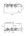
- a SOI wafer scale package 200 includes one mother chip 202, such as a processor (or memory device or combination thereof) formed on a top silicon layer (e.g., 43 of FIG. 1 ) to achieve high performance, and several daughter chips 204, 206, 208, 210 and 212. These chips may include for example, SRAM cache, eDRAM, NVRAM, FPGA, and high-speed RF interface chips mounted on the backside of the assembly 200. Through via connections 251 are illustratively shown in one area between the mother chip 202 and daughter chips 204-212. Vias and the chip placement and alignment need to be performed after appropriate planning. It is preferably that the mother and daughter chips be co-designed for the package 200 to ensure coaction, proper alignment/placement and proper functioning.
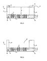
- package 300 where the mother chip 302 includes 3 macros M1, M2, and M3 (sub-chips).
- Package 300 indicates aspects to be considered during co-design of mother and daughter chips in a system.
- through via connections 351 are only permitted in the empty space between the adjacent macros (M1, M2, M3) and edges of the mother chips' substrate 340.
- Through vias 351 may be designated for different tasks, such as carrying power Vdd, or Vss or signals (Signal) as illustratively indicated in FIG. 16 .
- motherchip 302 may be comprised of multiple chips C1, C2, C3 and C4 and connected using macros, structures or subchips.
Landscapes
- Engineering & Computer Science (AREA)
- Microelectronics & Electronic Packaging (AREA)
- Power Engineering (AREA)
- Computer Hardware Design (AREA)
- Physics & Mathematics (AREA)
- Condensed Matter Physics & Semiconductors (AREA)
- General Physics & Mathematics (AREA)
- Manufacturing & Machinery (AREA)
- Internal Circuitry In Semiconductor Integrated Circuit Devices (AREA)
- Led Device Packages (AREA)
Abstract
Description
- The present invention relates to semiconductor processing and devices, and more particularly to devices and methods, which employ silicon-on-insulator (SOI) technology to provide a double-sided chip structure.
- As the relentless scaling of complementary metal oxide semiconductor (CMOS) technology approaches its physical limit, the integration of very large-scale integrated circuit (VLSI) systems on a package (SoP) becomes increasingly important. The integration of many different chips on a package is often not cost effective, due to the incompatibility between various chip technologies. For example, non-volatile random access memory (NVRAM) with floating gate devices and dynamic random access memory (DRAM) with deep trenches require additional masks and processing steps to fabricate. High-speed Gallium Arsenide (GaAs) chips are manufactured on a different substrate than a silicon chip.
- An efficient method to integrate different chips on a two-dimensional (2-D) or three-dimension (3-D) package can not only enhance circuit performance but also reduce manufacturing cost. If the chips are stacked vertically, the through vias should also be used to further reduce the interconnect delay and maximize circuit performance.
- Advanced three-dimensional wafer-to-wafer vertical stack integration technology has recently been developed to improve system performance. In
U.S. Patent No. 6,645,832 , entitled "Etch stop layer for silicon via etch in three-dimensional wafer-to-wafer vertical stack", a method of using nickel silicide (NiSi) as an etch stop layer for the silicon via etch is described. In a 3-D package, a dielectric layer is used to bond the two vertically stacked wafers, and a silicon via etch is required to provide electrical conductivity between the wafers. - The vias are formed by selectively etching through the silicon of the top wafer until stopped by the etch stop layer. The sidewalls of the silicon vias are coated with a layer of insulating material, forming a barrier layer. The vias are then filled with conductive material to provide electrical connection.
- In
U.S. Patent No. 6,762,076 , entitled "Process of vertically stacking multiple wafers supporting different active integrated circuit devices", a metal-to-metal bonding method is used to bond adjacent wafers and provide electrical connections. - In
U.S. Patent No. 6,355,501 , entitled "Three-dimensional chip stacking assembly", multiple silicon-on-insulator (SOI) chips are stacked together and interconnects between chips are accomplished by aligning prefabricated contacts at the top and bottom surfaces of the chips. Each chip is thinned down significantly by backside chemical-mechanical-polishing (CMP) to remove all the material behind the buried oxide layer. In the 3-D assembly, each SOI chip includes a handler making mechanical contact to a first metallization pattern, the first metallization pattern making electrical contact to a semiconductor device, and the semiconductor device making electrical contact to a second metallization pattern on the opposite surface of the semiconductor device. - In
U.S. Patent No. 6,737,297 , entitled "Process for making fine pitch connections between devices and structure made by the process", a method is disclosed to join two or more chips together on a temporary substrate with prefabricated global wirings by aligning the stud on the chip surface and the via on the temporary alignment substrate. The two-dimensional chip assembly is then transferred to a permanent support carrier with heat-sink devices, and the transparent plate of the temporary alignment structure is ablated and detached from the assembly. - In
U.S. Patent No. 6,607,938 , entitled "Wafer level stack chip package and method for manufacturing same", the semiconductor chips are stacked on the redistribution substrate. After multiple thin chips on the corresponding wafers are stacked together, the stack-chip structures are cut out from the stack-wafer assembly and the carrier material is then stripped away. - In
U.S. Patent No. 6,175,160 , entitled "Flip-chip having an on-chip cache memory", a flip-chip includes a semiconductor substrate with circuit elements formed on a first surface. A cache memory device is electrically couples to a plurality of electrical interconnects located in a cavity on the second surface of the semiconductor substrate. - In
U.S. Patent No. 6,730,541 , entitled "Wafer-scale assembly of chip-size packages", a polymer film carrying solder balls for each of the contact pads is aligned with the wafer. Infrared energy is applied to the backside of the wafer to uniformly heat the wafer. The process is then repeated to sequentially assemble an interposer and a second polymer film carrying solder balls. - A semiconductor package and a method for forming a semiconductor package are set out in claims 1 and 6, respectively.
- These and other objects, features and advantages of the present invention will become apparent from the following detailed description of illustrative embodiments thereof, which is to be read in connection with the accompanying drawings.
- Preferred embodiments of the present invention will now be described, by way of example only, with reference to the accompanying drawings in which:
-
FIG. 1 is a cross-sectional view of a silicon-on-insulator structure/wafer showing electronic components formed thereon; -
FIG. 2 is a cross-sectional view showing through vias etched, dielectric liners formed and filled with a conductive material in accordance with one embodiment of the present invention; -
FIG. 3 is a cross-sectional view showing a protective coating formed on a first side of the wafer in accordance with the present invention; -
FIG. 4 is a cross-sectional view showing polishing/etching of a silicon substrate portion of the wafer in preparation for etching in accordance with the present invention; -
FIG. 5 is a cross-sectional view showing silicon substrate (backside) photolithography patterning in accordance with the present invention; -
FIG. 6 is a cross-sectional view showing backside etching to form a cavity in accordance with the present invention; -
FIG. 7 is a cross-sectional view showing pockets opened around through vias within the cavity in accordance with the present invention; -
FIG. 8 is a cross-sectional view showing selective deposition of solder on through vias in accordance with the present invention; -
FIG. 9 is a cross-sectional view showing the placement of sub-chips into the backside cavity and aligning the sub-chips with the through vias in accordance with the present invention; -
FIG. 10 is a cross-sectional view showing soldering and bonding of the sub-chips to the through vias to permit the sub-chips and components of the original to coact to perform a function in accordance with the present invention; -
FIG. 11 is a cross-sectional view showing a thermally conductive underfill and deposition of a thermally conductive layer in accordance with the present invention; -
FIG. 12 is a cross-sectional view showing the protective coating being removed from the front side of the wafer in accordance with the present invention; -
FIG. 13 is a cross-sectional view showing front side global interconnect formation and C4 formation in accordance with the present invention; -
FIG. 14 is a cross-sectional view showing the formation of a backside heat sink in accordance with the present invention; -
FIG. 15 is a perspective view showing a plurality of sub-chips placed and connected by through vias to a mother chip in accordance with one embodiment of the present invention; and -
FIG. 16 is a top schematic view of a mother chip with daughter (sub-chips) placed therein showing through via placement and function in accordance with one embodiment of the present invention. - The present invention provides a low-cost and high-yield double-sided wafer scale package preferably on a silicon-on-insulator (SOI) wafer. A mother chip is formed on the front side of the SOI wafer with a fully or partially depleted body to achieve high performance. A plurality of thinned daughter chips are then mounted inside the cavities on the backside of the SOI wafer, opposite the mother chip. Through silicon and buried oxide, metal studs are fabricated to facilitate interconnection between the mother and daughter chips.
- Advantageously, the present methods do not need the chips to be transferred from a temporary carrier to a permanent carrier, which reduces the cost. Accordingly, by employing through via connections and cavity formation, sub-chips (daughter chips) can be directly diced out of a wafer and mounted on the backside of the mother chip. The method further avoids the use of vertical stacking in a 3-D package to facilitate heat dissipation. In addition, multiple chips manufactured in different technologies can be integrated on the same package.
- The double-sided package protocol adopts two-dimensional chip packaging schemes on both sides of the wafer. In the thin silicon layer on the front side of the SOI wafer, mother chips such as central processing units and serializer/deserializer (SerDes) chips are fabricated. The performance of these chips is boosted by the floating body effect as well as low junction capacitance.
- The floating body effect is an inherent characteristic of SOI MOSFETs. Since the potential of the body is not fixed, the holes that are injected into the body cause the potential in the body to rise, resulting in lower threshold voltage, higher drain current and faster gate. The buried oxide layer also eliminates the area junction capacitance between the source/drain diffusion and the substrate, which allows the transistor to operate faster with less capacitance to charge and discharge. With secondary components placed on the backside of the wafer, the mother chips will have smaller dimensions and higher yield than equivalent system-on-chip (SoC) designs.
- The remaining area on the front side of the SOI wafer can be used to form decoupling capacitors and other discrete devices. The backside of the SOI wafer may have thicker material that can be thinned down before etching to form the cavities for the daughter chips. The daughter chips that can be embedded in the cavities may include high-speed radio frequency (RF) input/output (I/O) chips, memory chips such as non-volatile random access memory (NVRAM), magnetic RAM (MRAM), ferroelectric RAM (FRAM), and embedded dynamic RAM (eDRAM) whose deep trench capacitor process is not fully compatible with conventional CMOS processes, decoupling capacitors, high-Q semiconductor inductors, and micro-electromechanical systems (MEMS).
- The present invention may form deep vias from the pads of the mother chips on the front side of the SOI wafer, through the buried oxide layer, to the pads of the daughter chips on the backside of the SOI wafer. These through vias not only provide the power supplies, signals and controls, but also enable the communication, testing, and monitoring of the mother and daughter chips. To fabricate the through vias, no devices or interconnects should be formed underneath the designated pads of the mother chip. Since the total thickness of the top silicon layer and the buried oxide layer is within a few hundred microns, the size of these through vias can be much smaller than a traditional multi-chip package.
- It is to be understood that the present invention will be described in terms of a given illustrative architecture having a SOI wafer; however, other architectures, structures, substrate materials and process features and steps may be varied within the scope of the present invention.
- Referring now in detail to the figures in which like numerals represent the same or similar elements and initially to
FIG. 1 , a silicon-on-insulator (SOI)wafer 10 with atop silicon layer 43, a buried dielectric (e.g., oxide)layer 42, and a bottom substrate 40 (e.g., silicon) are illustratively shown. Anintegrated circuit system 11 includesactive devices 44, metal interconnects 45, anddiscrete devices 48 formed on thesilicon wafer 10. The buriedoxide layer 42 onSOI wafer 10 may include a thickness of say, 5 micrometers or less. - Referring to
FIG. 2 ,trenches 50 may be formed. In one embodiment, high-density plasma reactive ion etching (RIE) can be used to createtrenches 50 down to thesilicon substrate 40 throughlayers vias 51, which permit other chips to be mounted on the backside of thewafer 10, and will be described herein. - Through
vias 51 are formed through atop silicon layer 43 after lithographic patterning, etching,sidewall dielectric coating 52, and metal or conductive filling 53. In one embodiment, the ratio of via depth to via size (e.g., trench width) may range from between about 1 to about 5. To etch a back end of line (BEOL) insulatingmaterial 32, thesilicon layer 43, and the buriedoxide layer 42, respectively, CF4, Cl2 and/or CF4 based plasma etching may be employed successively, with a proper end-point detection method. Such detection methods are known in the art. - To ensure that
vias 51 are extended below the buriedoxide layer 42, it may be necessary to over-etch the buriedoxide layer 42. Insulatingmaterials 52, such as the oxide/nitride sidewall spacers, are preferably employed to prevent the vias 51 from being shorted to any adjacent conductive layers, well regions, or the substrate layer. Thevias 51 can then be filled withconductive metal 53, such as copper, tungsten, aluminum, doped polycrystalline material, alloys and/or any other conductive material. A conformal chemical vapor deposition (CVD) deep-etch technique can be used to eliminate any void formation inside thevias 51 during the filling process. - Referring to
FIG. 3 , a layer ofprotective coating 60 such as oxide, nitride, oxy-nitride, or glass is formed on a top surface of thewafer 10 to protect it from being damaged during the backside processing. Other materials or protection schemes may also be employed. - Referring to
FIG. 4 , thesilicon substrate 40 on the backside of the wafer is thinned, by for example, chemical-mechanical polishing (CMP) or high-density plasma etching (e.g., RIE) to a proper thickness "d". It is preferable that "d" may be a few microns thicker than the thickest chip to be mounted on the backside. - Referring to
FIGS. 5 and 6 , aphotolithography pattern 64 is generated by applying aphotoresist 66 and patterning the resist 66 using known methods. Resist 66 is then employed as a mask in an etching process to form a backside cavity orcavities 68. The size of thecavity 68 should be slightly larger than the chip to be mounted inside (below the open surface) and margins should be provided in case of misalignment. Multiple chips may be placed inside thesame cavity 68. - The
cavities 68 are formed after etching and theconductive material 53 of throughvias 51 is exposed at the surface of the buriedoxide layer 42. The resist 66 is removed fromsubstrate 40. - Referring to
FIG. 7 , an extra etching step may be employed to open apocket 70 on top of each via 51 by thin photoresist patterning and exposure at the surface of the buriedoxide 42. Thepocket 70 formation serves during the ensuing bonding and soldering reflow steps to provide the space for solder to flow and thus form better contacts. - Referring to
FIG. 8 , a selective plating process may be employed to formsolder balls 74 on exposedstuds 53 invias 51 and inside thepockets 70. The process selectively forms metal onstuds 53. Low melting-temperature material is preferable in forming thesolder balls 74.Solder balls 74 may include tin or lead alloys and may employ a process similar to a controlled collapse chip connection (C4) bonding method. - Referring to
FIG. 9 , chips (sub-chips) 80 and 82 are illustratively shown making contact withstuds 53 ofvias 51.Chips cavity 68, and bonded to the mother chip (wafer 10). The depth (d) of thecavities 68 is preferably deeper than the thickness of all the daughter chips (80 and 82).Chips -
Chips cavity 68 havinggaps 84 therebetween and betweenwalls 86 andchips studs 53 withcontacts chip chips cavity 68. - A bonding process may include a temperature of about 400°C to be carried out to join solder balls for
contacts solder balls 74 for throughvias 51 for themother chip 10. - Referring to
FIG. 10 , collection ofexcessive bonding material 94 is shown inside thepocket areas 70.Chips vias 51. - Referring to
FIG. 11 , an under-fill process is employed to fill thegaps chips wafer 10 with a thermallyconductive agent 98, such as a thermal paste, or standard filling polymer or other fillers. It is preferred that theagent 98 be thermally conductive to promote heat dissipation, but act as an electrical insulator. The top surface of thecavity 68 may further be filled with a more thermallyconductive material 102 such as, for example, chemical vapor deposited (CVD) diamond. Ametal film 104 may also be formed on the backside ofwafer 10 to seal the daughter chips inside thecavities 68. - Referring to
FIG. 12 , after the daughter chips 80 and 82 are mounted on the backside, the topprotective layer 60 of a mother chip 120 (on wafer 10) can be stripped. This may be in preparation for further processing on the system such as global or local interconnects and vias, attaching other components or forming additional layers or features, etc. - Referring to
FIG. 13 ,more metal layers 106,contact pads 108, andC4 balls 110 can be formed on the front side of thewafer 10 ofmother chip 120. Further processing may be performed to form additional structures or to provide packaging forsystem 100. - A final double-
side chip assembly 100 can be cut from the wafer 10 (e.g., dicing the wafer to form chip packages), where each assembly has amother chip 120 on the front side and a plurality of daughter chips (e.g., 80 and 82) mounted on the backside. The buriedoxide layer 42 of theSOI wafer 10 is used as the holding plate for through via interconnection between themother chip 120 and daughter chips 80 and 82. - A
heat sink 111 can be mounted on the backside of the chip as illustratively shown inFIG. 14 .Heat sink 111 may be attached, e.g., using a thermal adhesive material, or may be formed be depositing materials and etching the material into a predetermined shape (e.g., fins and troughs). - Referring to
FIG. 15 , a SOIwafer scale package 200 includes onemother chip 202, such as a processor (or memory device or combination thereof) formed on a top silicon layer (e.g., 43 ofFIG. 1 ) to achieve high performance, andseveral daughter chips assembly 200. Through via connections 251 are illustratively shown in one area between themother chip 202 and daughter chips 204-212. Vias and the chip placement and alignment need to be performed after appropriate planning. It is preferably that the mother and daughter chips be co-designed for thepackage 200 to ensure coaction, proper alignment/placement and proper functioning. - Referring to
FIG. 16 , one example of apackage 300 where themother chip 302 includes 3 macros M1, M2, and M3 (sub-chips).Package 300 indicates aspects to be considered during co-design of mother and daughter chips in a system. In this embodiment, through viaconnections 351 are only permitted in the empty space between the adjacent macros (M1, M2, M3) and edges of the mother chips'substrate 340. Throughvias 351 may be designated for different tasks, such as carrying power Vdd, or Vss or signals (Signal) as illustratively indicated inFIG. 16 . In an alternate embodiment,motherchip 302 may be comprised of multiple chips C1, C2, C3 and C4 and connected using macros, structures or subchips. - Having described preferred embodiments of a device and method for fabricating double-sided SOI wafer scale package with buried oxide through via connections (which are intended to be illustrative and not limiting), it is noted that modifications and variations can be made by persons skilled in the art in light of the above teachings. It is therefore to be understood that changes may be made in the particular embodiments of the invention disclosed which are within the scope of the invention as outlined by the appended claims.
Claims (11)
- A semiconductor package, comprising:a wafer (10) having a first side including at least one electronic component (44.45.48), and a second side opposite the first side and forming a cavity (68);at least one chip (80,82) placed in the cavity (68);a portion of the wafer (10) comprising a through via (51), a portion of which is exposed by the cavity (68); and acontact (88,90) of the chip (80,82) being soldered to the through via (51), characterised by the cavity (68) having a pocket (70) around the through via (51).
- The package as recited in claim 1, wherein:the wafer (10) includes a silicon-on-insulator wafer (10);the first side includes a top silicon layer (43) and the second side includes a silicon substrate (40) wherein the top silicon layer (43) is separated from the silicon substrate (40) by a buried dielectric layer (42); andthe through via (51) is formed through the buried dielectric layer (42) to form a connection between the electronic component (44,45,48) and the at least one chip (80,82).
- The package as recited in claim 1, further comprising a thermally conductive fill material (98) at least partially surrounding the at least one chip (80,82).
- The package as recited in claim 1, further comprising a thermally conductive layer (102) formed over at least a portion of the at least one chip (80,82).
- The package as recited in claim 4, further comprising a heat sink (111) formed on the thermally conductive layer (102).
- A method for forming a semiconductor package, comprising the steps of:forming a through via (51) through a first side of a wafer (10), the first side of the wafer (10) including at least one electronic component (44,45,48);forming a cavity (68) on a second side of the wafer (10) exposing a portion of the through via (51), including opening a pocket (70) around the through via (51) in the cavity (68);selectively depositing solder to the exposed portion of the through via (51);placing at least one sub-chip (80,82) in the cavity (68) and connecting the sub-chip (80,82) to the through via (51), including soldering a contact (88,90) of the sub-chip (80,82) to the through via (51).
- The method as recited in claim 6, wherein the wafer (10) includes a silicon-on-insulator wafer (10) and the step of forming a through via (51) through a first side of a wafer (10) includes etching a via hole (50) through a top silicon layer (43) and a buried dielectric layer (42) and filling the via hole (50) with a conductor.
- The method as recited in claim 7, wherein the step of forming a cavity (68) on a second side of the wafer (10) exposing a portion of the through via (51) includes etching a silicon substrate (40) of the wafer (10) to expose the portion of the through via (51).
- The method as recited in claim 6, further comprising the step of underfilling the sub-chip (80,82) with a thermally conductive material.
- The method as recited in claim 6, further comprising the step of depositing a thermally conductive layer (102) over the sub-chip (80,82).
- The method as recited in claim 6, further comprising the step of providing a heat sink (111) for heat dissipation from the sub chip (80,82).
Applications Claiming Priority (2)
| Application Number | Priority Date | Filing Date | Title |
|---|---|---|---|
| US10/990,252 US7098070B2 (en) | 2004-11-16 | 2004-11-16 | Device and method for fabricating double-sided SOI wafer scale package with through via connections |
| PCT/EP2005/055734 WO2006053832A1 (en) | 2004-11-16 | 2005-11-03 | Device and method for fabricating double-sided soi wafer scale package with through via connections |
Publications (2)
| Publication Number | Publication Date |
|---|---|
| EP1851797A1 EP1851797A1 (en) | 2007-11-07 |
| EP1851797B1 true EP1851797B1 (en) | 2012-03-07 |
Family
ID=35677682
Family Applications (1)
| Application Number | Title | Priority Date | Filing Date |
|---|---|---|---|
| EP05807945A Not-in-force EP1851797B1 (en) | 2004-11-16 | 2005-11-03 | Device and method for fabricating double-sided soi wafer scale package with through via connections |
Country Status (7)
| Country | Link |
|---|---|
| US (3) | US7098070B2 (en) |
| EP (1) | EP1851797B1 (en) |
| JP (1) | JP2008521213A (en) |
| CN (1) | CN100481421C (en) |
| AT (1) | ATE548756T1 (en) |
| TW (1) | TWI351727B (en) |
| WO (1) | WO2006053832A1 (en) |
Cited By (1)
| Publication number | Priority date | Publication date | Assignee | Title |
|---|---|---|---|---|
| US9412736B2 (en) | 2014-06-05 | 2016-08-09 | Globalfoundries Inc. | Embedding semiconductor devices in silicon-on-insulator wafers connected using through silicon vias |
Families Citing this family (184)
| Publication number | Priority date | Publication date | Assignee | Title |
|---|---|---|---|---|
| US6551857B2 (en) | 1997-04-04 | 2003-04-22 | Elm Technology Corporation | Three dimensional structure integrated circuits |
| US6297548B1 (en) | 1998-06-30 | 2001-10-02 | Micron Technology, Inc. | Stackable ceramic FBGA for high thermal applications |
| AU2003255254A1 (en) | 2002-08-08 | 2004-02-25 | Glenn J. Leedy | Vertical system integration |
| WO2007000695A2 (en) * | 2005-06-29 | 2007-01-04 | Koninklijke Philips Electronics N.V. | Package, subassembly and methods of manufacturing thereof |
| JP4507101B2 (en) | 2005-06-30 | 2010-07-21 | エルピーダメモリ株式会社 | Semiconductor memory device and manufacturing method thereof |
| JP4979213B2 (en) * | 2005-08-31 | 2012-07-18 | オンセミコンダクター・トレーディング・リミテッド | Circuit board, circuit board manufacturing method, and circuit device |
| US20070126085A1 (en) * | 2005-12-02 | 2007-06-07 | Nec Electronics Corporation | Semiconductor device and method of manufacturing the same |
| EP1881527A1 (en) * | 2006-07-17 | 2008-01-23 | STMicroelectronics S.r.l. | Process for manufacturing a semiconductor wafer having SOI-insulated wells and semiconductor wafer thereby manufactured |
| JP5107539B2 (en) * | 2006-08-03 | 2012-12-26 | 新光電気工業株式会社 | Semiconductor device and manufacturing method of semiconductor device |
| US7545029B2 (en) * | 2006-08-18 | 2009-06-09 | Tessera, Inc. | Stack microelectronic assemblies |
| JP2008066481A (en) * | 2006-09-06 | 2008-03-21 | Shinko Electric Ind Co Ltd | Package, semiconductor device, manufacturing method of package and manufacturing method of semiconductor device |
| US7704874B1 (en) * | 2006-10-02 | 2010-04-27 | Newport Fab, Llc | Method for fabricating a frontside through-wafer via in a processed wafer and related structure |
| SE533579C2 (en) * | 2007-01-25 | 2010-10-26 | Silex Microsystems Ab | Method of microcapsulation and microcapsules |
| JP2009071095A (en) * | 2007-09-14 | 2009-04-02 | Spansion Llc | Method of manufacturing semiconductor device |
| US9001527B2 (en) * | 2008-02-18 | 2015-04-07 | Cyntec Co., Ltd. | Electronic package structure |
| US8824165B2 (en) | 2008-02-18 | 2014-09-02 | Cyntec Co. Ltd | Electronic package structure |
| TWI355068B (en) * | 2008-02-18 | 2011-12-21 | Cyntec Co Ltd | Electronic package structure |
| US8247267B2 (en) * | 2008-03-11 | 2012-08-21 | Taiwan Semiconductor Manufacturing Company, Ltd. | Wafer level IC assembly method |
| US8044755B2 (en) * | 2008-04-09 | 2011-10-25 | National Semiconductor Corporation | MEMS power inductor |
| US7705411B2 (en) * | 2008-04-09 | 2010-04-27 | National Semiconductor Corporation | MEMS-topped integrated circuit with a stress relief layer |
| US20090261416A1 (en) * | 2008-04-18 | 2009-10-22 | Wolfgang Raberg | Integrated mems device and control circuit |
| SG142321A1 (en) | 2008-04-24 | 2009-11-26 | Micron Technology Inc | Pre-encapsulated cavity interposer |
| WO2009147547A1 (en) * | 2008-06-02 | 2009-12-10 | Nxp B.V. | Electronic device and method of manufacturing an electronic device |
| US20090305463A1 (en) * | 2008-06-06 | 2009-12-10 | International Business Machines Corporation | System and Method for Thermal Optimized Chip Stacking |
| US7885494B2 (en) * | 2008-07-02 | 2011-02-08 | Sony Ericsson Mobile Communications Ab | Optical signaling for a package-on-package stack |
| US8005326B2 (en) * | 2008-07-10 | 2011-08-23 | Taiwan Semiconductor Manufacturing Company, Ltd. | Optical clock signal distribution using through-silicon vias |
| US8637953B2 (en) * | 2008-07-14 | 2014-01-28 | International Business Machines Corporation | Wafer scale membrane for three-dimensional integrated circuit device fabrication |
| US8384224B2 (en) * | 2008-08-08 | 2013-02-26 | International Business Machines Corporation | Through wafer vias and method of making same |
| US8035198B2 (en) * | 2008-08-08 | 2011-10-11 | International Business Machines Corporation | Through wafer via and method of making same |
| US8138036B2 (en) | 2008-08-08 | 2012-03-20 | International Business Machines Corporation | Through silicon via and method of fabricating same |
| US8299566B2 (en) | 2008-08-08 | 2012-10-30 | International Business Machines Corporation | Through wafer vias and method of making same |
| US7989950B2 (en) * | 2008-08-14 | 2011-08-02 | Stats Chippac Ltd. | Integrated circuit packaging system having a cavity |
| US7851925B2 (en) | 2008-09-19 | 2010-12-14 | Infineon Technologies Ag | Wafer level packaged MEMS integrated circuit |
| US8987868B1 (en) * | 2009-02-24 | 2015-03-24 | Xilinx, Inc. | Method and apparatus for programmable heterogeneous integration of stacked semiconductor die |
| JP2010287866A (en) * | 2009-06-15 | 2010-12-24 | Renesas Electronics Corp | Semiconductor device |
| US9466561B2 (en) | 2009-08-06 | 2016-10-11 | Rambus Inc. | Packaged semiconductor device for high performance memory and logic |
| US8063424B2 (en) * | 2009-11-16 | 2011-11-22 | International Business Machines Corporation | Embedded photodetector apparatus in a 3D CMOS chip stack |
| US8119431B2 (en) * | 2009-12-08 | 2012-02-21 | Freescale Semiconductor, Inc. | Method of forming a micro-electromechanical system (MEMS) having a gap stop |
| EP2339627A1 (en) * | 2009-12-24 | 2011-06-29 | Imec | Window interposed die packaging |
| US8901724B2 (en) * | 2009-12-29 | 2014-12-02 | Intel Corporation | Semiconductor package with embedded die and its methods of fabrication |
| US9219023B2 (en) * | 2010-01-19 | 2015-12-22 | Globalfoundries Inc. | 3D chip stack having encapsulated chip-in-chip |
| US9015023B2 (en) | 2010-05-05 | 2015-04-21 | Xilinx, Inc. | Device specific configuration of operating voltage |
| US9484279B2 (en) * | 2010-06-02 | 2016-11-01 | STATS ChipPAC Pte. Ltd. | Semiconductor device and method of forming EMI shielding layer with conductive material around semiconductor die |
| US8399292B2 (en) | 2010-06-30 | 2013-03-19 | International Business Machines Corporation | Fabricating a semiconductor chip with backside optical vias |
| US8598695B2 (en) | 2010-07-23 | 2013-12-03 | Tessera, Inc. | Active chip on carrier or laminated chip having microelectronic element embedded therein |
| JP5959516B2 (en) | 2010-08-18 | 2016-08-02 | ライフ テクノロジーズ コーポレーション | Microwell chemical coating method for electrochemical detection devices |
| US8518746B2 (en) | 2010-09-02 | 2013-08-27 | Stats Chippac, Ltd. | Semiconductor device and method of forming TSV semiconductor wafer with embedded semiconductor die |
| CN101976660B (en) * | 2010-09-10 | 2015-04-15 | 上海华虹宏力半导体制造有限公司 | Silicon-on-insulator (SOI) substrate silicon wafer with heat-radiating structure and preparation method thereof |
| US8470612B2 (en) | 2010-10-07 | 2013-06-25 | Infineon Technologies Ag | Integrated circuits with magnetic core inductors and methods of fabrications thereof |
| US9337116B2 (en) | 2010-10-28 | 2016-05-10 | Stats Chippac, Ltd. | Semiconductor device and method of forming stepped interposer for stacking and electrically connecting semiconductor die |
| TWI453864B (en) * | 2010-11-12 | 2014-09-21 | Ind Tech Res Inst | Semiconductor structure and manufacturing method thereof |
| DE102010056056A1 (en) * | 2010-12-23 | 2012-06-28 | Osram Opto Semiconductors Gmbh | Method for producing an electrical connection carrier |
| US9024408B2 (en) * | 2010-12-29 | 2015-05-05 | Stmicroelectronics, Inc. | Double side wafer process, method and device |
| KR101761834B1 (en) | 2011-01-28 | 2017-07-27 | 서울바이오시스 주식회사 | Wafer level led package and method of fabricating the same |
| CN102163590A (en) * | 2011-03-09 | 2011-08-24 | 中国科学院上海微系统与信息技术研究所 | Three-dimensional multi-chip encapsulation module based on buried substrate and method |
| US8338294B2 (en) | 2011-03-31 | 2012-12-25 | Soitec | Methods of forming bonded semiconductor structures including two or more processed semiconductor structures carried by a common substrate, and semiconductor structures formed by such methods |
| FR2973943B1 (en) * | 2011-04-08 | 2013-04-05 | Soitec Silicon On Insulator | METHODS OF FORMING BONDED SEMICONDUCTOR STRUCTURES COMPRISING TWO SEMICONDUCTOR STRUCTURES TREATED OR MORE SUPPORTED BY A COMMON SUBSTRATE, AND SEMICONDUCTOR STRUCTURES FORMED THEREFROM |
| US20120248621A1 (en) * | 2011-03-31 | 2012-10-04 | S.O.I.Tec Silicon On Insulator Technologies | Methods of forming bonded semiconductor structures, and semiconductor structures formed by such methods |
| US8970045B2 (en) * | 2011-03-31 | 2015-03-03 | Soitec | Methods for fabrication of semiconductor structures including interposers with conductive vias, and related structures and devices |
| US8803269B2 (en) | 2011-05-05 | 2014-08-12 | Cisco Technology, Inc. | Wafer scale packaging platform for transceivers |
| US8481425B2 (en) | 2011-05-16 | 2013-07-09 | United Microelectronics Corp. | Method for fabricating through-silicon via structure |
| US8822336B2 (en) | 2011-06-16 | 2014-09-02 | United Microelectronics Corp. | Through-silicon via forming method |
| US8828745B2 (en) | 2011-07-06 | 2014-09-09 | United Microelectronics Corp. | Method for manufacturing through-silicon via |
| US8497558B2 (en) * | 2011-07-14 | 2013-07-30 | Infineon Technologies Ag | System and method for wafer level packaging |
| US8518823B2 (en) | 2011-12-23 | 2013-08-27 | United Microelectronics Corp. | Through silicon via and method of forming the same |
| US8609529B2 (en) | 2012-02-01 | 2013-12-17 | United Microelectronics Corp. | Fabrication method and structure of through silicon via |
| TWI573203B (en) * | 2012-02-16 | 2017-03-01 | 索泰克公司 | Methods for fabrication of semiconductor structures including interposers with conductive vias, and related structures and devices |
| US8691600B2 (en) | 2012-05-02 | 2014-04-08 | United Microelectronics Corp. | Method for testing through-silicon-via (TSV) structures |
| US8691688B2 (en) | 2012-06-18 | 2014-04-08 | United Microelectronics Corp. | Method of manufacturing semiconductor structure |
| US9275933B2 (en) | 2012-06-19 | 2016-03-01 | United Microelectronics Corp. | Semiconductor device |
| US8900996B2 (en) | 2012-06-21 | 2014-12-02 | United Microelectronics Corp. | Through silicon via structure and method of fabricating the same |
| US8525296B1 (en) | 2012-06-26 | 2013-09-03 | United Microelectronics Corp. | Capacitor structure and method of forming the same |
| US8716856B2 (en) * | 2012-08-02 | 2014-05-06 | Globalfoundries Singapore Pte. Ltd. | Device with integrated power supply |
| US10094988B2 (en) * | 2012-08-31 | 2018-10-09 | Micron Technology, Inc. | Method of forming photonics structures |
| US8912844B2 (en) | 2012-10-09 | 2014-12-16 | United Microelectronics Corp. | Semiconductor structure and method for reducing noise therein |
| US9035457B2 (en) | 2012-11-29 | 2015-05-19 | United Microelectronics Corp. | Substrate with integrated passive devices and method of manufacturing the same |
| US8716104B1 (en) | 2012-12-20 | 2014-05-06 | United Microelectronics Corp. | Method of fabricating isolation structure |
| KR102190382B1 (en) | 2012-12-20 | 2020-12-11 | 삼성전자주식회사 | Semiconductor package |
| US9209121B2 (en) | 2013-02-01 | 2015-12-08 | Analog Devices, Inc. | Double-sided package |
| US9997443B2 (en) * | 2013-02-25 | 2018-06-12 | Infineon Technologies Ag | Through vias and methods of formation thereof |
| US9583414B2 (en) | 2013-10-31 | 2017-02-28 | Qorvo Us, Inc. | Silicon-on-plastic semiconductor device and method of making the same |
| US9812350B2 (en) | 2013-03-06 | 2017-11-07 | Qorvo Us, Inc. | Method of manufacture for a silicon-on-plastic semiconductor device with interfacial adhesion layer |
| US9061890B2 (en) * | 2013-03-13 | 2015-06-23 | Intel Corporation | Methods of forming buried electromechanical structures coupled with device substrates and structures formed thereby |
| KR102048251B1 (en) * | 2013-03-14 | 2019-11-25 | 삼성전자주식회사 | Memory chip package, memory system having the same and driving method thereof |
| US8884398B2 (en) | 2013-04-01 | 2014-11-11 | United Microelectronics Corp. | Anti-fuse structure and programming method thereof |
| US9000490B2 (en) | 2013-04-19 | 2015-04-07 | Xilinx, Inc. | Semiconductor package having IC dice and voltage tuners |
| US9287173B2 (en) | 2013-05-23 | 2016-03-15 | United Microelectronics Corp. | Through silicon via and process thereof |
| US9123730B2 (en) | 2013-07-11 | 2015-09-01 | United Microelectronics Corp. | Semiconductor device having through silicon trench shielding structure surrounding RF circuit |
| US9024416B2 (en) | 2013-08-12 | 2015-05-05 | United Microelectronics Corp. | Semiconductor structure |
| US8916471B1 (en) | 2013-08-26 | 2014-12-23 | United Microelectronics Corp. | Method for forming semiconductor structure having through silicon via for signal and shielding structure |
| US9048223B2 (en) | 2013-09-03 | 2015-06-02 | United Microelectronics Corp. | Package structure having silicon through vias connected to ground potential |
| US9117804B2 (en) | 2013-09-13 | 2015-08-25 | United Microelectronics Corporation | Interposer structure and manufacturing method thereof |
| TWI566395B (en) | 2013-11-18 | 2017-01-11 | 元太科技工業股份有限公司 | Organic light-emitting diode display and method of manufacturing the same |
| US9343359B2 (en) | 2013-12-25 | 2016-05-17 | United Microelectronics Corp. | Integrated structure and method for fabricating the same |
| US10340203B2 (en) | 2014-02-07 | 2019-07-02 | United Microelectronics Corp. | Semiconductor structure with through silicon via and method for fabricating and testing the same |
| EP3164886A4 (en) * | 2014-07-02 | 2018-06-20 | Intel Corporation | Electronic assembly that includes stacked electronic devices |
| US9731959B2 (en) | 2014-09-25 | 2017-08-15 | Analog Devices, Inc. | Integrated device packages having a MEMS die sealed in a cavity by a processor die and method of manufacturing the same |
| CN104332455B (en) * | 2014-09-25 | 2017-03-08 | 武汉新芯集成电路制造有限公司 | A kind of piece semiconductor-on-insulator device architecture based on silicon hole and preparation method thereof |
| US10085352B2 (en) | 2014-10-01 | 2018-09-25 | Qorvo Us, Inc. | Method for manufacturing an integrated circuit package |
| US9236328B1 (en) * | 2014-10-27 | 2016-01-12 | International Business Machines Corporation | Electrical and optical through-silicon-via (TSV) |
| US9530709B2 (en) | 2014-11-03 | 2016-12-27 | Qorvo Us, Inc. | Methods of manufacturing a printed circuit module having a semiconductor device with a protective layer in place of a low-resistivity handle layer |
| US9533878B2 (en) | 2014-12-11 | 2017-01-03 | Analog Devices, Inc. | Low stress compact device packages |
| US9859225B2 (en) | 2015-05-15 | 2018-01-02 | Skyworks Solutions, Inc. | Backside cavity formation in semiconductor devices |
| US10594355B2 (en) * | 2015-06-30 | 2020-03-17 | Skyworks Solutions, Inc. | Devices and methods related to radio-frequency filters on silicon-on-insulator substrate |
| KR20170011366A (en) * | 2015-07-22 | 2017-02-02 | 삼성전자주식회사 | Semiconductor chip and semiconductor package having the same |
| US9786641B2 (en) | 2015-08-13 | 2017-10-10 | International Business Machines Corporation | Packaging optoelectronic components and CMOS circuitry using silicon-on-insulator substrates for photonics applications |
| US10276495B2 (en) | 2015-09-11 | 2019-04-30 | Qorvo Us, Inc. | Backside semiconductor die trimming |
| US9859382B2 (en) | 2015-12-04 | 2018-01-02 | Globalfoundries Inc. | Integrated CMOS wafers |
| US10256863B2 (en) * | 2016-01-11 | 2019-04-09 | Qualcomm Incorporated | Monolithic integration of antenna switch and diplexer |
| US10090262B2 (en) | 2016-05-09 | 2018-10-02 | Qorvo Us, Inc. | Microelectronics package with inductive element and magnetically enhanced mold compound component |
| US10773952B2 (en) | 2016-05-20 | 2020-09-15 | Qorvo Us, Inc. | Wafer-level package with enhanced performance |
| US10468329B2 (en) | 2016-07-18 | 2019-11-05 | Qorvo Us, Inc. | Thermally enhanced semiconductor package having field effect transistors with back-gate feature |
| US10784149B2 (en) | 2016-05-20 | 2020-09-22 | Qorvo Us, Inc. | Air-cavity module with enhanced device isolation |
| US10103080B2 (en) | 2016-06-10 | 2018-10-16 | Qorvo Us, Inc. | Thermally enhanced semiconductor package with thermal additive and process for making the same |
| EP3497719B1 (en) | 2016-08-12 | 2020-06-10 | Qorvo Us, Inc. | Wafer-level package with enhanced performance |
| WO2018031995A1 (en) | 2016-08-12 | 2018-02-15 | Qorvo Us, Inc. | Wafer-level package with enhanced performance |
| JP7022112B2 (en) | 2016-08-12 | 2022-02-17 | コーボ ユーエス,インコーポレイティド | Wafer level package with improved performance |
| US9837302B1 (en) * | 2016-08-26 | 2017-12-05 | Qualcomm Incorporated | Methods of forming a device having semiconductor devices on two sides of a buried dielectric layer |
| US10020335B2 (en) | 2016-09-09 | 2018-07-10 | Omnivision Technologies, Inc. | Short-resistant chip-scale package |
| US10109502B2 (en) | 2016-09-12 | 2018-10-23 | Qorvo Us, Inc. | Semiconductor package with reduced parasitic coupling effects and process for making the same |
| US10276548B2 (en) * | 2016-09-14 | 2019-04-30 | Taiwan Semiconductor Manufacturing Company, Ltd. | Semiconductor packages having dummy connectors and methods of forming same |
| US10090339B2 (en) | 2016-10-21 | 2018-10-02 | Qorvo Us, Inc. | Radio frequency (RF) switch |
| US10749518B2 (en) | 2016-11-18 | 2020-08-18 | Qorvo Us, Inc. | Stacked field-effect transistor switch |
| US20180151291A1 (en) * | 2016-11-29 | 2018-05-31 | Qualcomm Incorporated | Inductor with embedded diode |
| US10068831B2 (en) | 2016-12-09 | 2018-09-04 | Qorvo Us, Inc. | Thermally enhanced semiconductor package and process for making the same |
| US10468736B2 (en) | 2017-02-08 | 2019-11-05 | Aptiv Technologies Limited | Radar assembly with ultra wide band waveguide to substrate integrated waveguide transition |
| WO2018165899A1 (en) * | 2017-03-15 | 2018-09-20 | Hong Kong R&D Centre for Logistics and Supply Chain Management Enabling Technologies Limited | A radio frequency communication guiding device |
| US10755992B2 (en) | 2017-07-06 | 2020-08-25 | Qorvo Us, Inc. | Wafer-level packaging for enhanced performance |
| US10784233B2 (en) | 2017-09-05 | 2020-09-22 | Qorvo Us, Inc. | Microelectronics package with self-aligned stacked-die assembly |
| US10366972B2 (en) * | 2017-09-05 | 2019-07-30 | Qorvo Us, Inc. | Microelectronics package with self-aligned stacked-die assembly |
| US10998273B2 (en) * | 2017-12-22 | 2021-05-04 | Hrl Laboratories, Llc | Hybrid integrated circuit architecture |
| US11527482B2 (en) * | 2017-12-22 | 2022-12-13 | Hrl Laboratories, Llc | Hybrid integrated circuit architecture |
| US11536800B2 (en) * | 2017-12-22 | 2022-12-27 | Hrl Laboratories, Llc | Method and apparatus to increase radar range |
| US11152363B2 (en) | 2018-03-28 | 2021-10-19 | Qorvo Us, Inc. | Bulk CMOS devices with enhanced performance and methods of forming the same utilizing bulk CMOS process |
| WO2019195428A1 (en) | 2018-04-04 | 2019-10-10 | Qorvo Us, Inc. | Gallium-nitride-based module with enhanced electrical performance and process for making the same |
| US12046505B2 (en) | 2018-04-20 | 2024-07-23 | Qorvo Us, Inc. | RF devices with enhanced performance and methods of forming the same utilizing localized SOI formation |
| US10804246B2 (en) | 2018-06-11 | 2020-10-13 | Qorvo Us, Inc. | Microelectronics package with vertically stacked dies |
| US20200006193A1 (en) | 2018-07-02 | 2020-01-02 | Qorvo Us, Inc. | Rf devices with enhanced performance and methods of forming the same |
| WO2020029096A1 (en) * | 2018-08-07 | 2020-02-13 | 深圳市为通博科技有限责任公司 | Chip package structure and manufacturing method therefor |
| US10964554B2 (en) | 2018-10-10 | 2021-03-30 | Qorvo Us, Inc. | Wafer-level fan-out package with enhanced performance |
| US11069590B2 (en) | 2018-10-10 | 2021-07-20 | Qorvo Us, Inc. | Wafer-level fan-out package with enhanced performance |
| WO2020077499A1 (en) * | 2018-10-15 | 2020-04-23 | 深圳市汇顶科技股份有限公司 | Integrated device having thin film transistor device and preparation method therefor |
| US10957537B2 (en) | 2018-11-12 | 2021-03-23 | Hrl Laboratories, Llc | Methods to design and uniformly co-fabricate small vias and large cavities through a substrate |
| US11646242B2 (en) | 2018-11-29 | 2023-05-09 | Qorvo Us, Inc. | Thermally enhanced semiconductor package with at least one heat extractor and process for making the same |
| CN111341750B (en) | 2018-12-19 | 2024-03-01 | 奥特斯奥地利科技与系统技术有限公司 | Component carrier comprising an electrically conductive base structure and method of manufacture |
| US11387157B2 (en) | 2019-01-23 | 2022-07-12 | Qorvo Us, Inc. | RF devices with enhanced performance and methods of forming the same |
| KR20210129656A (en) | 2019-01-23 | 2021-10-28 | 코르보 유에스, 인크. | RF semiconductor device and method of forming same |
| US12057374B2 (en) | 2019-01-23 | 2024-08-06 | Qorvo Us, Inc. | RF devices with enhanced performance and methods of forming the same |
| US12046483B2 (en) | 2019-01-23 | 2024-07-23 | Qorvo Us, Inc. | RF devices with enhanced performance and methods of forming the same |
| US12046570B2 (en) | 2019-01-23 | 2024-07-23 | Qorvo Us, Inc. | RF devices with enhanced performance and methods of forming the same |
| US11473191B2 (en) * | 2019-02-27 | 2022-10-18 | Applied Materials, Inc. | Method for creating a dielectric filled nanostructured silica substrate for flat optical devices |
| US11527808B2 (en) * | 2019-04-29 | 2022-12-13 | Aptiv Technologies Limited | Waveguide launcher |
| JP7232137B2 (en) * | 2019-06-25 | 2023-03-02 | ルネサスエレクトロニクス株式会社 | Semiconductor device and its manufacturing method |
| US11581289B2 (en) | 2019-07-30 | 2023-02-14 | Stmicroelectronics Pte Ltd | Multi-chip package |
| US11264358B2 (en) | 2019-09-11 | 2022-03-01 | Google Llc | ASIC package with photonics and vertical power delivery |
| US11296005B2 (en) | 2019-09-24 | 2022-04-05 | Analog Devices, Inc. | Integrated device package including thermally conductive element and method of manufacturing same |
| US12074086B2 (en) | 2019-11-01 | 2024-08-27 | Qorvo Us, Inc. | RF devices with nanotube particles for enhanced performance and methods of forming the same |
| US11646289B2 (en) | 2019-12-02 | 2023-05-09 | Qorvo Us, Inc. | RF devices with enhanced performance and methods of forming the same |
| US11923238B2 (en) | 2019-12-12 | 2024-03-05 | Qorvo Us, Inc. | Method of forming RF devices with enhanced performance including attaching a wafer to a support carrier by a bonding technique without any polymer adhesive |
| US11276668B2 (en) | 2020-02-12 | 2022-03-15 | Google Llc | Backside integrated voltage regulator for integrated circuits |
| JP2021174955A (en) * | 2020-04-30 | 2021-11-01 | ルネサスエレクトロニクス株式会社 | Semiconductor device and manufacturing method for the same |
| JP2021190440A (en) * | 2020-05-25 | 2021-12-13 | ソニーセミコンダクタソリューションズ株式会社 | Semiconductor device, manufacturing method thereof, and electronic apparatus |
| US11551993B2 (en) * | 2020-08-28 | 2023-01-10 | Ge Aviation Systems Llc | Power overlay module and method of assembling |
| US11972970B1 (en) | 2020-09-01 | 2024-04-30 | Hrl Laboratories, Llc | Singulation process for chiplets |
| US11362436B2 (en) | 2020-10-02 | 2022-06-14 | Aptiv Technologies Limited | Plastic air-waveguide antenna with conductive particles |
| US11757166B2 (en) | 2020-11-10 | 2023-09-12 | Aptiv Technologies Limited | Surface-mount waveguide for vertical transitions of a printed circuit board |
| US11626668B2 (en) | 2020-12-18 | 2023-04-11 | Aptiv Technologies Limited | Waveguide end array antenna to reduce grating lobes and cross-polarization |
| US11901601B2 (en) | 2020-12-18 | 2024-02-13 | Aptiv Technologies Limited | Waveguide with a zigzag for suppressing grating lobes |
| US11749883B2 (en) | 2020-12-18 | 2023-09-05 | Aptiv Technologies Limited | Waveguide with radiation slots and parasitic elements for asymmetrical coverage |
| US11502420B2 (en) | 2020-12-18 | 2022-11-15 | Aptiv Technologies Limited | Twin line fed dipole array antenna |
| US11681015B2 (en) | 2020-12-18 | 2023-06-20 | Aptiv Technologies Limited | Waveguide with squint alteration |
| US11444364B2 (en) | 2020-12-22 | 2022-09-13 | Aptiv Technologies Limited | Folded waveguide for antenna |
| US11668787B2 (en) | 2021-01-29 | 2023-06-06 | Aptiv Technologies Limited | Waveguide with lobe suppression |
| US12058804B2 (en) | 2021-02-09 | 2024-08-06 | Aptiv Technologies AG | Formed waveguide antennas of a radar assembly |
| WO2022186857A1 (en) | 2021-03-05 | 2022-09-09 | Qorvo Us, Inc. | Selective etching process for si-ge and doped epitaxial silicon |
| US11721905B2 (en) | 2021-03-16 | 2023-08-08 | Aptiv Technologies Limited | Waveguide with a beam-forming feature with radiation slots |
| US11616306B2 (en) | 2021-03-22 | 2023-03-28 | Aptiv Technologies Limited | Apparatus, method and system comprising an air waveguide antenna having a single layer material with air channels therein which is interfaced with a circuit board |
| EP4084222A1 (en) | 2021-04-30 | 2022-11-02 | Aptiv Technologies Limited | Dielectric loaded waveguide for low loss signal distributions and small form factor antennas |
| US11973268B2 (en) | 2021-05-03 | 2024-04-30 | Aptiv Technologies AG | Multi-layered air waveguide antenna with layer-to-layer connections |
| US11962085B2 (en) | 2021-05-13 | 2024-04-16 | Aptiv Technologies AG | Two-part folded waveguide having a sinusoidal shape channel including horn shape radiating slots formed therein which are spaced apart by one-half wavelength |
| CN115643791A (en) * | 2021-07-20 | 2023-01-24 | 安徽寒武纪信息科技有限公司 | System-on-a-chip, method of forming the same, and readable storage medium |
| US11616282B2 (en) | 2021-08-03 | 2023-03-28 | Aptiv Technologies Limited | Transition between a single-ended port and differential ports having stubs that match with input impedances of the single-ended and differential ports |
| US20230122242A1 (en) * | 2021-10-15 | 2023-04-20 | Hrl Laboratories, Llc | Thermal Isolation Between Embedded MECA Modules |
| US20230245993A1 (en) * | 2022-02-03 | 2023-08-03 | Ciena Corporation | Enhanced Thermal Control of a Hybrid Chip Assembly |
Family Cites Families (25)
| Publication number | Priority date | Publication date | Assignee | Title |
|---|---|---|---|---|
| JPH0521539A (en) * | 1991-07-12 | 1993-01-29 | Hitachi Ltd | Semiconductor device and computer |
| JP2943950B2 (en) * | 1991-08-22 | 1999-08-30 | 本田技研工業株式会社 | Semiconductor device and manufacturing method thereof |
| JP2823029B2 (en) * | 1992-03-30 | 1998-11-11 | 日本電気株式会社 | Multi-chip module |
| US5394490A (en) | 1992-08-11 | 1995-02-28 | Hitachi, Ltd. | Semiconductor device having an optical waveguide interposed in the space between electrode members |
| US5786635A (en) | 1996-12-16 | 1998-07-28 | International Business Machines Corporation | Electronic package with compressible heatsink structure |
| JPH10186185A (en) | 1996-12-19 | 1998-07-14 | Fuji Xerox Co Ltd | Optical bus and its manufacture, and signal processor |
| US6300686B1 (en) | 1997-10-02 | 2001-10-09 | Matsushita Electric Industrial Co., Ltd. | Semiconductor chip bonded to a thermal conductive sheet having a filled through hole for electrical connection |
| US6730541B2 (en) * | 1997-11-20 | 2004-05-04 | Texas Instruments Incorporated | Wafer-scale assembly of chip-size packages |
| EP0926726A1 (en) * | 1997-12-16 | 1999-06-30 | STMicroelectronics S.r.l. | Fabrication process and electronic device having front-back through contacts for bonding onto boards |
| DE19813239C1 (en) * | 1998-03-26 | 1999-12-23 | Fraunhofer Ges Forschung | Wiring method for manufacturing a vertical integrated circuit structure and vertical integrated circuit structure |
| US6175160B1 (en) * | 1999-01-08 | 2001-01-16 | Intel Corporation | Flip-chip having an on-chip cache memory |
| WO2000074134A1 (en) * | 1999-05-27 | 2000-12-07 | Fraunhofer-Gesellschaft zur Förderung der angewandten Forschung e.V. | Method for the vertical integration of electric components by |
| JP4360577B2 (en) * | 2000-03-29 | 2009-11-11 | 京セラ株式会社 | Semiconductor device |
| US6355501B1 (en) * | 2000-09-21 | 2002-03-12 | International Business Machines Corporation | Three-dimensional chip stacking assembly |
| US6444560B1 (en) * | 2000-09-26 | 2002-09-03 | International Business Machines Corporation | Process for making fine pitch connections between devices and structure made by the process |
| JP2002156561A (en) * | 2000-11-17 | 2002-05-31 | Minolta Co Ltd | Optical integrated module |
| FR2817399B1 (en) * | 2000-11-30 | 2003-10-31 | St Microelectronics Sa | MULTIFUNCTIONAL ELECTRONIC CHIP |
| KR100394808B1 (en) * | 2001-07-19 | 2003-08-14 | 삼성전자주식회사 | Wafer level stack chip package and method for manufacturing the same |
| US6787916B2 (en) | 2001-09-13 | 2004-09-07 | Tru-Si Technologies, Inc. | Structures having a substrate with a cavity and having an integrated circuit bonded to a contact pad located in the cavity |
| WO2003063570A2 (en) * | 2002-01-24 | 2003-07-31 | Massachusetts Institute Of Technology | A method and system for magnetically assisted statistical assembly of wafers |
| US6762076B2 (en) * | 2002-02-20 | 2004-07-13 | Intel Corporation | Process of vertically stacking multiple wafers supporting different active integrated circuit (IC) devices |
| US6645832B2 (en) * | 2002-02-20 | 2003-11-11 | Intel Corporation | Etch stop layer for silicon (Si) via etch in three-dimensional (3-D) wafer-to-wafer vertical stack |
| JP2003282817A (en) * | 2002-03-27 | 2003-10-03 | Matsushita Electric Ind Co Ltd | Semiconductor device and its manufacturing method |
| TWI231579B (en) * | 2002-12-31 | 2005-04-21 | Advanced Semiconductor Eng | Flip chip package |
| US6872589B2 (en) * | 2003-02-06 | 2005-03-29 | Kulicke & Soffa Investments, Inc. | High density chip level package for the packaging of integrated circuits and method to manufacture same |
-
2004
- 2004-11-16 US US10/990,252 patent/US7098070B2/en active Active
-
2005
- 2005-11-03 EP EP05807945A patent/EP1851797B1/en not_active Not-in-force
- 2005-11-03 JP JP2007540633A patent/JP2008521213A/en active Pending
- 2005-11-03 WO PCT/EP2005/055734 patent/WO2006053832A1/en active Application Filing
- 2005-11-03 CN CNB2005800359390A patent/CN100481421C/en active Active
- 2005-11-03 AT AT05807945T patent/ATE548756T1/en active
- 2005-11-14 TW TW094139868A patent/TWI351727B/en not_active IP Right Cessation
-
2006
- 2006-01-04 US US11/325,105 patent/US7489025B2/en active Active
-
2008
- 2008-08-27 US US12/199,063 patent/US7736949B2/en active Active
Cited By (1)
| Publication number | Priority date | Publication date | Assignee | Title |
|---|---|---|---|---|
| US9412736B2 (en) | 2014-06-05 | 2016-08-09 | Globalfoundries Inc. | Embedding semiconductor devices in silicon-on-insulator wafers connected using through silicon vias |
Also Published As
| Publication number | Publication date |
|---|---|
| TWI351727B (en) | 2011-11-01 |
| US7098070B2 (en) | 2006-08-29 |
| TW200634946A (en) | 2006-10-01 |
| US20060105496A1 (en) | 2006-05-18 |
| US7489025B2 (en) | 2009-02-10 |
| ATE548756T1 (en) | 2012-03-15 |
| CN101044618A (en) | 2007-09-26 |
| CN100481421C (en) | 2009-04-22 |
| EP1851797A1 (en) | 2007-11-07 |
| JP2008521213A (en) | 2008-06-19 |
| US20060113598A1 (en) | 2006-06-01 |
| US7736949B2 (en) | 2010-06-15 |
| US20080318360A1 (en) | 2008-12-25 |
| WO2006053832A1 (en) | 2006-05-26 |
Similar Documents
| Publication | Publication Date | Title |
|---|---|---|
| EP1851797B1 (en) | Device and method for fabricating double-sided soi wafer scale package with through via connections | |
| US20230138732A1 (en) | Transistor level interconnection methodologies utilizing 3d interconnects | |
| TWI588966B (en) | Integrated circuit assemblies with reinforcement frames, and methods of manufacture | |
| US8367472B2 (en) | Method of fabricating a 3-D device | |
| US7056813B2 (en) | Methods of forming backside connections on a wafer stack | |
| US8097955B2 (en) | Interconnect structures and methods | |
| WO2015183959A1 (en) | Structure and method for integrated circuits packaging with increased density | |
| US20070087528A1 (en) | Method and structure for vertically-stacked device contact | |
| CN214672598U (en) | Three-dimensional semiconductor device structure and three-dimensional semiconductor device | |
| US10262922B2 (en) | Semiconductor device having through-silicon-via and methods of forming the same | |
| US20240290755A1 (en) | Semiconductor devices and methods of manufacture | |
| KR20240090930A (en) | Semiconductor device assemblies including monolithic silicon structures for heat dissipation and methods of manufacturing the same | |
| KR20210035037A (en) | Semiconductor devices and methods of manufacture | |
| US20240038686A1 (en) | Semiconductor packages and methods of manufacturing thereof | |
| TWI849935B (en) | Intra-bonding semiconductor integrated circuit chips | |
| KR102642271B1 (en) | Integrated circuit package and method | |
| US11664315B2 (en) | Structure with interconnection die and method of making same | |
| US20240096848A1 (en) | Integrated circuit package and method | |
| TW202326963A (en) | Semiconductor device assemblies including monolithic silicon structures for thermal dissipation and methods of making the same | |
| TW202406018A (en) | Interconnecting structure with high aspect ratio tsv and method for forming the same | |
| TW202410373A (en) | Semiconductor package and manufacturing method thereof | |
| TW202129894A (en) | Selective interconnects in back-end-of-line metallization stacks of integrated circuitry |
Legal Events
| Date | Code | Title | Description |
|---|---|---|---|
| PUAI | Public reference made under article 153(3) epc to a published international application that has entered the european phase |
Free format text: ORIGINAL CODE: 0009012 |
|
| 17P | Request for examination filed |
Effective date: 20070613 |
|
| AK | Designated contracting states |
Kind code of ref document: A1 Designated state(s): AT BE BG CH CY CZ DE DK EE ES FI FR GB GR HU IE IS IT LI LT LU LV MC NL PL PT RO SE SI SK TR |
|
| DAX | Request for extension of the european patent (deleted) | ||
| 17Q | First examination report despatched |
Effective date: 20110513 |
|
| GRAP | Despatch of communication of intention to grant a patent |
Free format text: ORIGINAL CODE: EPIDOSNIGR1 |
|
| GRAS | Grant fee paid |
Free format text: ORIGINAL CODE: EPIDOSNIGR3 |
|
| GRAA | (expected) grant |
Free format text: ORIGINAL CODE: 0009210 |
|
| AK | Designated contracting states |
Kind code of ref document: B1 Designated state(s): AT BE BG CH CY CZ DE DK EE ES FI FR GB GR HU IE IS IT LI LT LU LV MC NL PL PT RO SE SI SK TR |
|
| REG | Reference to a national code |
Ref country code: GB Ref legal event code: FG4D |
|
| REG | Reference to a national code |
Ref country code: DE Ref legal event code: R081 Ref document number: 602005033077 Country of ref document: DE Owner name: GLOBALFOUNDRIES INC., KY Free format text: FORMER OWNER: INTERNATIONAL BUSINESS MACHINES CORPORATION, ARMONK, N.Y., US |
|
| REG | Reference to a national code |
Ref country code: AT Ref legal event code: REF Ref document number: 548756 Country of ref document: AT Kind code of ref document: T Effective date: 20120315 Ref country code: CH Ref legal event code: EP |
|
| REG | Reference to a national code |
Ref country code: IE Ref legal event code: FG4D |
|
| REG | Reference to a national code |
Ref country code: CH Ref legal event code: NV Representative=s name: IBM RESEARCH GMBH ZURICH RESEARCH LABORATORY INTEL |
|
| REG | Reference to a national code |
Ref country code: DE Ref legal event code: R096 Ref document number: 602005033077 Country of ref document: DE Effective date: 20120503 |
|
| REG | Reference to a national code |
Ref country code: GB Ref legal event code: 746 Effective date: 20120416 |
|
| REG | Reference to a national code |
Ref country code: DE Ref legal event code: R084 Ref document number: 602005033077 Country of ref document: DE Effective date: 20120330 |
|
| REG | Reference to a national code |
Ref country code: NL Ref legal event code: VDEP Effective date: 20120307 |
|
| PG25 | Lapsed in a contracting state [announced via postgrant information from national office to epo] |
Ref country code: NL Free format text: LAPSE BECAUSE OF FAILURE TO SUBMIT A TRANSLATION OF THE DESCRIPTION OR TO PAY THE FEE WITHIN THE PRESCRIBED TIME-LIMIT Effective date: 20120307 Ref country code: LT Free format text: LAPSE BECAUSE OF FAILURE TO SUBMIT A TRANSLATION OF THE DESCRIPTION OR TO PAY THE FEE WITHIN THE PRESCRIBED TIME-LIMIT Effective date: 20120307 |
|
| LTIE | Lt: invalidation of european patent or patent extension |
Effective date: 20120307 |
|
| PG25 | Lapsed in a contracting state [announced via postgrant information from national office to epo] |
Ref country code: LV Free format text: LAPSE BECAUSE OF FAILURE TO SUBMIT A TRANSLATION OF THE DESCRIPTION OR TO PAY THE FEE WITHIN THE PRESCRIBED TIME-LIMIT Effective date: 20120307 Ref country code: GR Free format text: LAPSE BECAUSE OF FAILURE TO SUBMIT A TRANSLATION OF THE DESCRIPTION OR TO PAY THE FEE WITHIN THE PRESCRIBED TIME-LIMIT Effective date: 20120608 Ref country code: FI Free format text: LAPSE BECAUSE OF FAILURE TO SUBMIT A TRANSLATION OF THE DESCRIPTION OR TO PAY THE FEE WITHIN THE PRESCRIBED TIME-LIMIT Effective date: 20120307 |
|
| REG | Reference to a national code |
Ref country code: AT Ref legal event code: MK05 Ref document number: 548756 Country of ref document: AT Kind code of ref document: T Effective date: 20120307 |
|
| PG25 | Lapsed in a contracting state [announced via postgrant information from national office to epo] |
Ref country code: CY Free format text: LAPSE BECAUSE OF FAILURE TO SUBMIT A TRANSLATION OF THE DESCRIPTION OR TO PAY THE FEE WITHIN THE PRESCRIBED TIME-LIMIT Effective date: 20120307 |
|
| PG25 | Lapsed in a contracting state [announced via postgrant information from national office to epo] |
Ref country code: SE Free format text: LAPSE BECAUSE OF FAILURE TO SUBMIT A TRANSLATION OF THE DESCRIPTION OR TO PAY THE FEE WITHIN THE PRESCRIBED TIME-LIMIT Effective date: 20120307 Ref country code: EE Free format text: LAPSE BECAUSE OF FAILURE TO SUBMIT A TRANSLATION OF THE DESCRIPTION OR TO PAY THE FEE WITHIN THE PRESCRIBED TIME-LIMIT Effective date: 20120307 Ref country code: PL Free format text: LAPSE BECAUSE OF FAILURE TO SUBMIT A TRANSLATION OF THE DESCRIPTION OR TO PAY THE FEE WITHIN THE PRESCRIBED TIME-LIMIT Effective date: 20120307 Ref country code: BE Free format text: LAPSE BECAUSE OF FAILURE TO SUBMIT A TRANSLATION OF THE DESCRIPTION OR TO PAY THE FEE WITHIN THE PRESCRIBED TIME-LIMIT Effective date: 20120307 Ref country code: RO Free format text: LAPSE BECAUSE OF FAILURE TO SUBMIT A TRANSLATION OF THE DESCRIPTION OR TO PAY THE FEE WITHIN THE PRESCRIBED TIME-LIMIT Effective date: 20120307 Ref country code: CZ Free format text: LAPSE BECAUSE OF FAILURE TO SUBMIT A TRANSLATION OF THE DESCRIPTION OR TO PAY THE FEE WITHIN THE PRESCRIBED TIME-LIMIT Effective date: 20120307 Ref country code: SI Free format text: LAPSE BECAUSE OF FAILURE TO SUBMIT A TRANSLATION OF THE DESCRIPTION OR TO PAY THE FEE WITHIN THE PRESCRIBED TIME-LIMIT Effective date: 20120307 Ref country code: IS Free format text: LAPSE BECAUSE OF FAILURE TO SUBMIT A TRANSLATION OF THE DESCRIPTION OR TO PAY THE FEE WITHIN THE PRESCRIBED TIME-LIMIT Effective date: 20120707 |
|
| PG25 | Lapsed in a contracting state [announced via postgrant information from national office to epo] |
Ref country code: PT Free format text: LAPSE BECAUSE OF FAILURE TO SUBMIT A TRANSLATION OF THE DESCRIPTION OR TO PAY THE FEE WITHIN THE PRESCRIBED TIME-LIMIT Effective date: 20120709 Ref country code: SK Free format text: LAPSE BECAUSE OF FAILURE TO SUBMIT A TRANSLATION OF THE DESCRIPTION OR TO PAY THE FEE WITHIN THE PRESCRIBED TIME-LIMIT Effective date: 20120307 |
|
| PLBE | No opposition filed within time limit |
Free format text: ORIGINAL CODE: 0009261 |
|
| STAA | Information on the status of an ep patent application or granted ep patent |
Free format text: STATUS: NO OPPOSITION FILED WITHIN TIME LIMIT |
|
| PG25 | Lapsed in a contracting state [announced via postgrant information from national office to epo] |
Ref country code: DK Free format text: LAPSE BECAUSE OF FAILURE TO SUBMIT A TRANSLATION OF THE DESCRIPTION OR TO PAY THE FEE WITHIN THE PRESCRIBED TIME-LIMIT Effective date: 20120307 Ref country code: AT Free format text: LAPSE BECAUSE OF FAILURE TO SUBMIT A TRANSLATION OF THE DESCRIPTION OR TO PAY THE FEE WITHIN THE PRESCRIBED TIME-LIMIT Effective date: 20120307 |
|
| 26N | No opposition filed |
Effective date: 20121210 |
|
| PG25 | Lapsed in a contracting state [announced via postgrant information from national office to epo] |
Ref country code: IT Free format text: LAPSE BECAUSE OF FAILURE TO SUBMIT A TRANSLATION OF THE DESCRIPTION OR TO PAY THE FEE WITHIN THE PRESCRIBED TIME-LIMIT Effective date: 20120307 |
|
| REG | Reference to a national code |
Ref country code: DE Ref legal event code: R097 Ref document number: 602005033077 Country of ref document: DE Effective date: 20121210 |
|
| PG25 | Lapsed in a contracting state [announced via postgrant information from national office to epo] |
Ref country code: ES Free format text: LAPSE BECAUSE OF FAILURE TO SUBMIT A TRANSLATION OF THE DESCRIPTION OR TO PAY THE FEE WITHIN THE PRESCRIBED TIME-LIMIT Effective date: 20120618 |
|
| REG | Reference to a national code |
Ref country code: CH Ref legal event code: PL |
|
| PG25 | Lapsed in a contracting state [announced via postgrant information from national office to epo] |
Ref country code: BG Free format text: LAPSE BECAUSE OF FAILURE TO SUBMIT A TRANSLATION OF THE DESCRIPTION OR TO PAY THE FEE WITHIN THE PRESCRIBED TIME-LIMIT Effective date: 20120607 Ref country code: CH Free format text: LAPSE BECAUSE OF NON-PAYMENT OF DUE FEES Effective date: 20121130 Ref country code: LI Free format text: LAPSE BECAUSE OF NON-PAYMENT OF DUE FEES Effective date: 20121130 |
|
| REG | Reference to a national code |
Ref country code: IE Ref legal event code: MM4A |
|
| REG | Reference to a national code |
Ref country code: FR Ref legal event code: ST Effective date: 20130731 |
|
| PG25 | Lapsed in a contracting state [announced via postgrant information from national office to epo] |
Ref country code: IE Free format text: LAPSE BECAUSE OF NON-PAYMENT OF DUE FEES Effective date: 20121103 |
|
| PG25 | Lapsed in a contracting state [announced via postgrant information from national office to epo] |
Ref country code: FR Free format text: LAPSE BECAUSE OF NON-PAYMENT OF DUE FEES Effective date: 20121130 |
|
| PG25 | Lapsed in a contracting state [announced via postgrant information from national office to epo] |
Ref country code: MC Free format text: LAPSE BECAUSE OF NON-PAYMENT OF DUE FEES Effective date: 20121130 Ref country code: TR Free format text: LAPSE BECAUSE OF FAILURE TO SUBMIT A TRANSLATION OF THE DESCRIPTION OR TO PAY THE FEE WITHIN THE PRESCRIBED TIME-LIMIT Effective date: 20120307 |
|
| PG25 | Lapsed in a contracting state [announced via postgrant information from national office to epo] |
Ref country code: LU Free format text: LAPSE BECAUSE OF NON-PAYMENT OF DUE FEES Effective date: 20121103 |
|
| PG25 | Lapsed in a contracting state [announced via postgrant information from national office to epo] |
Ref country code: HU Free format text: LAPSE BECAUSE OF FAILURE TO SUBMIT A TRANSLATION OF THE DESCRIPTION OR TO PAY THE FEE WITHIN THE PRESCRIBED TIME-LIMIT Effective date: 20051103 |
|
| PGFP | Annual fee paid to national office [announced via postgrant information from national office to epo] |
Ref country code: GB Payment date: 20151028 Year of fee payment: 11 |
|
| REG | Reference to a national code |
Ref country code: DE Ref legal event code: R082 Ref document number: 602005033077 Country of ref document: DE Representative=s name: RICHARDT PATENTANWAELTE PARTG MBB, DE Ref country code: DE Ref legal event code: R081 Ref document number: 602005033077 Country of ref document: DE Owner name: GLOBALFOUNDRIES INC., KY Free format text: FORMER OWNER: INTERNATIONAL BUSINESS MACHINES CORPORATION, ARMONK, N.Y., US |
|
| REG | Reference to a national code |
Ref country code: DE Ref legal event code: R081 Ref document number: 602005033077 Country of ref document: DE Owner name: GLOBALFOUNDRIES INC., KY Free format text: FORMER OWNER: GLOBALFOUNDRIES US 2 LLC (N.D.GES.DES STAATES DELAWARE), HOPEWELL JUNCTION, N.Y., US Ref country code: DE Ref legal event code: R082 Ref document number: 602005033077 Country of ref document: DE Representative=s name: RICHARDT PATENTANWAELTE PARTG MBB, DE |
|
| GBPC | Gb: european patent ceased through non-payment of renewal fee |
Effective date: 20161103 |
|
| PG25 | Lapsed in a contracting state [announced via postgrant information from national office to epo] |
Ref country code: GB Free format text: LAPSE BECAUSE OF NON-PAYMENT OF DUE FEES Effective date: 20161103 |
|
| PGFP | Annual fee paid to national office [announced via postgrant information from national office to epo] |
Ref country code: DE Payment date: 20181023 Year of fee payment: 14 |
|
| REG | Reference to a national code |
Ref country code: DE Ref legal event code: R119 Ref document number: 602005033077 Country of ref document: DE |
|
| PG25 | Lapsed in a contracting state [announced via postgrant information from national office to epo] |
Ref country code: DE Free format text: LAPSE BECAUSE OF NON-PAYMENT OF DUE FEES Effective date: 20200603 |