EP3176543A1 - Circuit board mounting structure and sensor using same - Google Patents
Circuit board mounting structure and sensor using same Download PDFInfo
- Publication number
- EP3176543A1 EP3176543A1 EP15827155.1A EP15827155A EP3176543A1 EP 3176543 A1 EP3176543 A1 EP 3176543A1 EP 15827155 A EP15827155 A EP 15827155A EP 3176543 A1 EP3176543 A1 EP 3176543A1
- Authority
- EP
- European Patent Office
- Prior art keywords
- circuit board
- resin
- printed circuit
- circuit module
- mold
- Prior art date
- Legal status (The legal status is an assumption and is not a legal conclusion. Google has not performed a legal analysis and makes no representation as to the accuracy of the status listed.)
- Granted
Links
Images









Classifications
-
- G—PHYSICS
- G01—MEASURING; TESTING
- G01F—MEASURING VOLUME, VOLUME FLOW, MASS FLOW OR LIQUID LEVEL; METERING BY VOLUME
- G01F1/00—Measuring the volume flow or mass flow of fluid or fluent solid material wherein the fluid passes through a meter in a continuous flow
- G01F1/68—Measuring the volume flow or mass flow of fluid or fluent solid material wherein the fluid passes through a meter in a continuous flow by using thermal effects
- G01F1/684—Structural arrangements; Mounting of elements, e.g. in relation to fluid flow
- G01F1/6845—Micromachined devices
-
- G—PHYSICS
- G01—MEASURING; TESTING
- G01F—MEASURING VOLUME, VOLUME FLOW, MASS FLOW OR LIQUID LEVEL; METERING BY VOLUME
- G01F1/00—Measuring the volume flow or mass flow of fluid or fluent solid material wherein the fluid passes through a meter in a continuous flow
- G01F1/05—Measuring the volume flow or mass flow of fluid or fluent solid material wherein the fluid passes through a meter in a continuous flow by using mechanical effects
- G01F1/34—Measuring the volume flow or mass flow of fluid or fluent solid material wherein the fluid passes through a meter in a continuous flow by using mechanical effects by measuring pressure or differential pressure
- G01F1/36—Measuring the volume flow or mass flow of fluid or fluent solid material wherein the fluid passes through a meter in a continuous flow by using mechanical effects by measuring pressure or differential pressure the pressure or differential pressure being created by the use of flow constriction
- G01F1/38—Measuring the volume flow or mass flow of fluid or fluent solid material wherein the fluid passes through a meter in a continuous flow by using mechanical effects by measuring pressure or differential pressure the pressure or differential pressure being created by the use of flow constriction the pressure or differential pressure being measured by means of a movable element, e.g. diaphragm, piston, Bourdon tube or flexible capsule
-
- G—PHYSICS
- G01—MEASURING; TESTING
- G01F—MEASURING VOLUME, VOLUME FLOW, MASS FLOW OR LIQUID LEVEL; METERING BY VOLUME
- G01F1/00—Measuring the volume flow or mass flow of fluid or fluent solid material wherein the fluid passes through a meter in a continuous flow
- G01F1/68—Measuring the volume flow or mass flow of fluid or fluent solid material wherein the fluid passes through a meter in a continuous flow by using thermal effects
- G01F1/684—Structural arrangements; Mounting of elements, e.g. in relation to fluid flow
- G01F1/688—Structural arrangements; Mounting of elements, e.g. in relation to fluid flow using a particular type of heating, cooling or sensing element
- G01F1/69—Structural arrangements; Mounting of elements, e.g. in relation to fluid flow using a particular type of heating, cooling or sensing element of resistive type
- G01F1/692—Thin-film arrangements
-
- H—ELECTRICITY
- H05—ELECTRIC TECHNIQUES NOT OTHERWISE PROVIDED FOR
- H05K—PRINTED CIRCUITS; CASINGS OR CONSTRUCTIONAL DETAILS OF ELECTRIC APPARATUS; MANUFACTURE OF ASSEMBLAGES OF ELECTRICAL COMPONENTS
- H05K1/00—Printed circuits
- H05K1/18—Printed circuits structurally associated with non-printed electric components
- H05K1/181—Printed circuits structurally associated with non-printed electric components associated with surface mounted components
-
- H—ELECTRICITY
- H05—ELECTRIC TECHNIQUES NOT OTHERWISE PROVIDED FOR
- H05K—PRINTED CIRCUITS; CASINGS OR CONSTRUCTIONAL DETAILS OF ELECTRIC APPARATUS; MANUFACTURE OF ASSEMBLAGES OF ELECTRICAL COMPONENTS
- H05K1/00—Printed circuits
- H05K1/18—Printed circuits structurally associated with non-printed electric components
- H05K1/182—Printed circuits structurally associated with non-printed electric components associated with components mounted in printed circuit boards [PCB], e.g. insert-mounted components [IMC]
- H05K1/183—Printed circuits structurally associated with non-printed electric components associated with components mounted in printed circuit boards [PCB], e.g. insert-mounted components [IMC] associated with components mounted in and supported by recessed areas of the PCBs
-
- H—ELECTRICITY
- H05—ELECTRIC TECHNIQUES NOT OTHERWISE PROVIDED FOR
- H05K—PRINTED CIRCUITS; CASINGS OR CONSTRUCTIONAL DETAILS OF ELECTRIC APPARATUS; MANUFACTURE OF ASSEMBLAGES OF ELECTRICAL COMPONENTS
- H05K3/00—Apparatus or processes for manufacturing printed circuits
- H05K3/22—Secondary treatment of printed circuits
- H05K3/28—Applying non-metallic protective coatings
- H05K3/284—Applying non-metallic protective coatings for encapsulating mounted components
-
- H—ELECTRICITY
- H10—SEMICONDUCTOR DEVICES; ELECTRIC SOLID-STATE DEVICES NOT OTHERWISE PROVIDED FOR
- H10W—GENERIC PACKAGES, INTERCONNECTIONS, CONNECTORS OR OTHER CONSTRUCTIONAL DETAILS OF DEVICES COVERED BY CLASS H10
- H10W70/00—Package substrates; Interposers; Redistribution layers [RDL]
- H10W70/60—Insulating or insulated package substrates; Interposers; Redistribution layers
- H10W70/62—Insulating or insulated package substrates; Interposers; Redistribution layers characterised by their interconnections
- H10W70/65—Shapes or dispositions of interconnections
-
- H—ELECTRICITY
- H10—SEMICONDUCTOR DEVICES; ELECTRIC SOLID-STATE DEVICES NOT OTHERWISE PROVIDED FOR
- H10W—GENERIC PACKAGES, INTERCONNECTIONS, CONNECTORS OR OTHER CONSTRUCTIONAL DETAILS OF DEVICES COVERED BY CLASS H10
- H10W74/00—Encapsulations, e.g. protective coatings
- H10W74/01—Manufacture or treatment
- H10W74/016—Manufacture or treatment using moulds
-
- H—ELECTRICITY
- H10—SEMICONDUCTOR DEVICES; ELECTRIC SOLID-STATE DEVICES NOT OTHERWISE PROVIDED FOR
- H10W—GENERIC PACKAGES, INTERCONNECTIONS, CONNECTORS OR OTHER CONSTRUCTIONAL DETAILS OF DEVICES COVERED BY CLASS H10
- H10W74/00—Encapsulations, e.g. protective coatings
- H10W74/10—Encapsulations, e.g. protective coatings characterised by their shape or disposition
- H10W74/111—Encapsulations, e.g. protective coatings characterised by their shape or disposition the semiconductor body being completely enclosed
- H10W74/114—Encapsulations, e.g. protective coatings characterised by their shape or disposition the semiconductor body being completely enclosed by a substrate and the encapsulations
-
- H—ELECTRICITY
- H10—SEMICONDUCTOR DEVICES; ELECTRIC SOLID-STATE DEVICES NOT OTHERWISE PROVIDED FOR
- H10W—GENERIC PACKAGES, INTERCONNECTIONS, CONNECTORS OR OTHER CONSTRUCTIONAL DETAILS OF DEVICES COVERED BY CLASS H10
- H10W76/00—Containers; Fillings or auxiliary members therefor; Seals
- H10W76/10—Containers or parts thereof
- H10W76/12—Containers or parts thereof characterised by their shape
- H10W76/15—Containers comprising an insulating or insulated base
- H10W76/157—Containers comprising an insulating or insulated base having interconnections parallel to the insulating or insulated base
-
- H—ELECTRICITY
- H05—ELECTRIC TECHNIQUES NOT OTHERWISE PROVIDED FOR
- H05K—PRINTED CIRCUITS; CASINGS OR CONSTRUCTIONAL DETAILS OF ELECTRIC APPARATUS; MANUFACTURE OF ASSEMBLAGES OF ELECTRICAL COMPONENTS
- H05K2201/00—Indexing scheme relating to printed circuits covered by H05K1/00
- H05K2201/10—Details of components or other objects attached to or integrated in a printed circuit board
- H05K2201/10007—Types of components
- H05K2201/10151—Sensor
-
- H—ELECTRICITY
- H05—ELECTRIC TECHNIQUES NOT OTHERWISE PROVIDED FOR
- H05K—PRINTED CIRCUITS; CASINGS OR CONSTRUCTIONAL DETAILS OF ELECTRIC APPARATUS; MANUFACTURE OF ASSEMBLAGES OF ELECTRICAL COMPONENTS
- H05K2201/00—Indexing scheme relating to printed circuits covered by H05K1/00
- H05K2201/10—Details of components or other objects attached to or integrated in a printed circuit board
- H05K2201/10613—Details of electrical connections of non-printed components, e.g. special leads
- H05K2201/10954—Other details of electrical connections
- H05K2201/10977—Encapsulated connections
-
- H—ELECTRICITY
- H05—ELECTRIC TECHNIQUES NOT OTHERWISE PROVIDED FOR
- H05K—PRINTED CIRCUITS; CASINGS OR CONSTRUCTIONAL DETAILS OF ELECTRIC APPARATUS; MANUFACTURE OF ASSEMBLAGES OF ELECTRICAL COMPONENTS
- H05K2203/00—Indexing scheme relating to apparatus or processes for manufacturing printed circuits covered by H05K3/00
- H05K2203/13—Moulding and encapsulation; Deposition techniques; Protective layers
- H05K2203/1305—Moulding and encapsulation
- H05K2203/1316—Moulded encapsulation of mounted components
-
- H—ELECTRICITY
- H05—ELECTRIC TECHNIQUES NOT OTHERWISE PROVIDED FOR
- H05K—PRINTED CIRCUITS; CASINGS OR CONSTRUCTIONAL DETAILS OF ELECTRIC APPARATUS; MANUFACTURE OF ASSEMBLAGES OF ELECTRICAL COMPONENTS
- H05K2203/00—Indexing scheme relating to apparatus or processes for manufacturing printed circuits covered by H05K3/00
- H05K2203/13—Moulding and encapsulation; Deposition techniques; Protective layers
- H05K2203/1305—Moulding and encapsulation
- H05K2203/1327—Moulding over PCB locally or completely
-
- H—ELECTRICITY
- H05—ELECTRIC TECHNIQUES NOT OTHERWISE PROVIDED FOR
- H05K—PRINTED CIRCUITS; CASINGS OR CONSTRUCTIONAL DETAILS OF ELECTRIC APPARATUS; MANUFACTURE OF ASSEMBLAGES OF ELECTRICAL COMPONENTS
- H05K3/00—Apparatus or processes for manufacturing printed circuits
- H05K3/22—Secondary treatment of printed circuits
- H05K3/28—Applying non-metallic protective coatings
-
- H—ELECTRICITY
- H10—SEMICONDUCTOR DEVICES; ELECTRIC SOLID-STATE DEVICES NOT OTHERWISE PROVIDED FOR
- H10W—GENERIC PACKAGES, INTERCONNECTIONS, CONNECTORS OR OTHER CONSTRUCTIONAL DETAILS OF DEVICES COVERED BY CLASS H10
- H10W42/00—Arrangements for protection of devices
- H10W42/121—Arrangements for protection of devices protecting against mechanical damage
-
- H—ELECTRICITY
- H10—SEMICONDUCTOR DEVICES; ELECTRIC SOLID-STATE DEVICES NOT OTHERWISE PROVIDED FOR
- H10W—GENERIC PACKAGES, INTERCONNECTIONS, CONNECTORS OR OTHER CONSTRUCTIONAL DETAILS OF DEVICES COVERED BY CLASS H10
- H10W70/00—Package substrates; Interposers; Redistribution layers [RDL]
- H10W70/60—Insulating or insulated package substrates; Interposers; Redistribution layers
- H10W70/62—Insulating or insulated package substrates; Interposers; Redistribution layers characterised by their interconnections
- H10W70/63—Vias, e.g. via plugs
-
- H—ELECTRICITY
- H10—SEMICONDUCTOR DEVICES; ELECTRIC SOLID-STATE DEVICES NOT OTHERWISE PROVIDED FOR
- H10W—GENERIC PACKAGES, INTERCONNECTIONS, CONNECTORS OR OTHER CONSTRUCTIONAL DETAILS OF DEVICES COVERED BY CLASS H10
- H10W70/00—Package substrates; Interposers; Redistribution layers [RDL]
- H10W70/60—Insulating or insulated package substrates; Interposers; Redistribution layers
- H10W70/67—Insulating or insulated package substrates; Interposers; Redistribution layers characterised by their insulating layers or insulating parts
- H10W70/68—Shapes or dispositions thereof
- H10W70/682—Shapes or dispositions thereof comprising holes having chips therein
-
- H—ELECTRICITY
- H10—SEMICONDUCTOR DEVICES; ELECTRIC SOLID-STATE DEVICES NOT OTHERWISE PROVIDED FOR
- H10W—GENERIC PACKAGES, INTERCONNECTIONS, CONNECTORS OR OTHER CONSTRUCTIONAL DETAILS OF DEVICES COVERED BY CLASS H10
- H10W72/00—Interconnections or connectors in packages
- H10W72/01—Manufacture or treatment
- H10W72/015—Manufacture or treatment of bond wires
- H10W72/01515—Forming coatings
-
- H—ELECTRICITY
- H10—SEMICONDUCTOR DEVICES; ELECTRIC SOLID-STATE DEVICES NOT OTHERWISE PROVIDED FOR
- H10W—GENERIC PACKAGES, INTERCONNECTIONS, CONNECTORS OR OTHER CONSTRUCTIONAL DETAILS OF DEVICES COVERED BY CLASS H10
- H10W72/00—Interconnections or connectors in packages
- H10W72/071—Connecting or disconnecting
- H10W72/075—Connecting or disconnecting of bond wires
- H10W72/07551—Connecting or disconnecting of bond wires characterised by changes in properties of the bond wires during the connecting
- H10W72/07552—Connecting or disconnecting of bond wires characterised by changes in properties of the bond wires during the connecting changes in structures or sizes
-
- H—ELECTRICITY
- H10—SEMICONDUCTOR DEVICES; ELECTRIC SOLID-STATE DEVICES NOT OTHERWISE PROVIDED FOR
- H10W—GENERIC PACKAGES, INTERCONNECTIONS, CONNECTORS OR OTHER CONSTRUCTIONAL DETAILS OF DEVICES COVERED BY CLASS H10
- H10W72/00—Interconnections or connectors in packages
- H10W72/50—Bond wires
- H10W72/521—Structures or relative sizes of bond wires
- H10W72/527—Multiple bond wires having different sizes
-
- H—ELECTRICITY
- H10—SEMICONDUCTOR DEVICES; ELECTRIC SOLID-STATE DEVICES NOT OTHERWISE PROVIDED FOR
- H10W—GENERIC PACKAGES, INTERCONNECTIONS, CONNECTORS OR OTHER CONSTRUCTIONAL DETAILS OF DEVICES COVERED BY CLASS H10
- H10W72/00—Interconnections or connectors in packages
- H10W72/50—Bond wires
- H10W72/541—Dispositions of bond wires
- H10W72/5445—Dispositions of bond wires being orthogonal to a side surface of the chip, e.g. parallel arrangements
-
- H—ELECTRICITY
- H10—SEMICONDUCTOR DEVICES; ELECTRIC SOLID-STATE DEVICES NOT OTHERWISE PROVIDED FOR
- H10W—GENERIC PACKAGES, INTERCONNECTIONS, CONNECTORS OR OTHER CONSTRUCTIONAL DETAILS OF DEVICES COVERED BY CLASS H10
- H10W72/00—Interconnections or connectors in packages
- H10W72/851—Dispositions of multiple connectors or interconnections
- H10W72/874—On different surfaces
- H10W72/884—Die-attach connectors and bond wires
-
- H—ELECTRICITY
- H10—SEMICONDUCTOR DEVICES; ELECTRIC SOLID-STATE DEVICES NOT OTHERWISE PROVIDED FOR
- H10W—GENERIC PACKAGES, INTERCONNECTIONS, CONNECTORS OR OTHER CONSTRUCTIONAL DETAILS OF DEVICES COVERED BY CLASS H10
- H10W74/00—Encapsulations, e.g. protective coatings
-
- H—ELECTRICITY
- H10—SEMICONDUCTOR DEVICES; ELECTRIC SOLID-STATE DEVICES NOT OTHERWISE PROVIDED FOR
- H10W—GENERIC PACKAGES, INTERCONNECTIONS, CONNECTORS OR OTHER CONSTRUCTIONAL DETAILS OF DEVICES COVERED BY CLASS H10
- H10W90/00—Package configurations
- H10W90/701—Package configurations characterised by the relative positions of pads or connectors relative to package parts
- H10W90/731—Package configurations characterised by the relative positions of pads or connectors relative to package parts of die-attach connectors
- H10W90/734—Package configurations characterised by the relative positions of pads or connectors relative to package parts of die-attach connectors between a chip and a stacked insulating package substrate, interposer or RDL
-
- H—ELECTRICITY
- H10—SEMICONDUCTOR DEVICES; ELECTRIC SOLID-STATE DEVICES NOT OTHERWISE PROVIDED FOR
- H10W—GENERIC PACKAGES, INTERCONNECTIONS, CONNECTORS OR OTHER CONSTRUCTIONAL DETAILS OF DEVICES COVERED BY CLASS H10
- H10W90/00—Package configurations
- H10W90/701—Package configurations characterised by the relative positions of pads or connectors relative to package parts
- H10W90/751—Package configurations characterised by the relative positions of pads or connectors relative to package parts of bond wires
- H10W90/754—Package configurations characterised by the relative positions of pads or connectors relative to package parts of bond wires between a chip and a stacked insulating package substrate, interposer or RDL
-
- Y—GENERAL TAGGING OF NEW TECHNOLOGICAL DEVELOPMENTS; GENERAL TAGGING OF CROSS-SECTIONAL TECHNOLOGIES SPANNING OVER SEVERAL SECTIONS OF THE IPC; TECHNICAL SUBJECTS COVERED BY FORMER USPC CROSS-REFERENCE ART COLLECTIONS [XRACs] AND DIGESTS
- Y02—TECHNOLOGIES OR APPLICATIONS FOR MITIGATION OR ADAPTATION AGAINST CLIMATE CHANGE
- Y02P—CLIMATE CHANGE MITIGATION TECHNOLOGIES IN THE PRODUCTION OR PROCESSING OF GOODS
- Y02P70/00—Climate change mitigation technologies in the production process for final industrial or consumer products
- Y02P70/50—Manufacturing or production processes characterised by the final manufactured product
Definitions
- the present invention relates to a circuit board mounting structure and a sensor using the same.
- Patent Literature 1 Japanese Unexamined Patent Application Publication No. 2012-163504 (Patent Literature 1), which describes as follows: "In an air flow measurement device with a structure in which a sensing element for measuring the physical quantity, such as temperature and humidity, is provided on a circuit board in which an electronic circuit is formed, the electronic drive circuit is placed in a housing and the sensing element is exposed to the intake air. At least one or more insulating layers are provided between the circuit board and a glass or resin coated layer. Further, a conductor wiring for connecting the sensing element to the electronic drive circuit is provided below the insulating layer".
- Patent Literature 1 Japanese Unexamined Patent Application Publication No. 2012-163504
- An object of the present invention is to provide a circuit board structure that can reduce deformation of a circuit board in insert molding of the circuit board.
- a structure formed by insert molding according to the present invention is an insert molded article that includes a printed circuit board mounted with semiconductor parts, in which the area where the semiconductor parts on the printed circuit board are not mounted is covered with a first resin.
- a second resin with an elastic modulus smaller than the elastic modulus of the material of the printed circuit board is placed on the outside of the area where the main surface of the printed circuit board overlaps the first resin.
- the present invention it is possible to suppress deformation and crack of a circuit board when the circuit board is formed by insert molding.
- the internal combustion engine of a car or vehicle is provided with modules including an electronic circuit, such as a sensor, an engine control unit, and an electronic control throttle.
- modules including an electronic circuit, such as a sensor, an engine control unit, and an electronic control throttle.
- a circuit board on which semiconductor parts are mounted is used.
- the circuit board is accommodated within a housing.
- the circuit board on which the semiconductor parts are mounted has been secured to a plastic housing by bonding with an adhesive.
- this method requires a process of applying and curing the adhesive, which reduces the throughput of the module manufacturing process.
- insert molding there is also another method called insert molding.
- Insert molding is the method of placing a circuit board within a mold in such a way that the circuit board is secured by pouring resin around the perimeter of the circuit board to form a plastic housing.
- melting resin is directly brought into contact with the circuit board, so that the circuit board can be bonded to the housing simultaneously when the resin is solidified. In this way, it is possible to simplify the bonding process.
- the housing resin is brought into contact with the semiconductor parts on the circuit board, a load due to shrinkage of the resin can be easily applied to the semiconductor as well as the joint portion of the semiconductor parts and the circuit board.
- the housing should be formed by pouring resin in such a way that the mounting area of the semiconductor parts is enclosed by the mold so that the mounting area and the peripheral board are not covered with the resin.
- this method blocks the resin by pressing the mold against the board.
- the board may be deformed by stress from the mold and deformation and crack may occur in the board.
- an intake air flow sensor which is mounted on the internal combustion engine of a car.
- the intake air flow sensor is the flow sensor for measuring the flow rate of gas (air), which is provided to help control the intake air flow by an electronic fuel injector that is mounted on the internal combustion engine.
- the intake air flow sensor uses a sensor chip with a thin-walled diaphragm, in which the data measured by the sensor chip is collected and adjusted by a control chip and is output to the outside.
- Fig. 1 shows a circuit module mounted with a semiconductor chip having a control circuit and the like.
- Fig. 2 is a cross-sectional view of the semiconductor chip taken along line A-A of Fig. 1 , showing the mounting structure of the circuit module.
- the circuit module is mounted with a first semiconductor chip 3 including a diaphragm 2 on a printed circuit board 1 of a material which is, for example, a lamination of glass fiber and resin, as well as a second semiconductor chip 4 including a control circuit.
- the printed circuit board 1 and the first semiconductor chip 3 are attached with an adhesive 5. Further, the printed circuit board 1 and the second semiconductor chip 4 are attached with a second adhesive 6.
- a conductor wiring 8 and a wire pad 9 for the conductor wiring are formed inside the printed circuit board 1, a conductor wiring 8 and a wire pad 9 for the conductor wiring are formed.
- the first semiconductor chip 3 and the second conductor chip 4 are connected by a wire 7, the conductive wiring 8, and the wire pad 9. Further, the second semiconductor chip 4 is connected to the conductor wiring 8 by the wire 7.
- a potting 10 is provided in order to protect the wire 7.
- thermosetting resin such as epoxy resin and polyurethane resin
- thermoplastic resin such as polyimide and acrylic resin
- a filler such as glass or mica can be mixed in the resin.
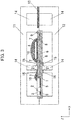
- Fig. 3 shows the mold structure for molding the circuit module while exposing the area where the semiconductor parts are mounted.
- the mounted circuit module and a connector lead 13 are placed into a mold including an upper mold 11 and a lower mold 12, in which a hollow portion 14 is formed by clamping the circuit module by a clamp portion 15 of the mold. Then, a resin 16 is injected into the hollow portion 14.
- the wire pad 9 of the circuit module is connected to the connector lead 13 by a wire 17. Further, in order to protect a circuit chamber 18 which is a space including the wire 17, an upper cover 19 and a lower cover 20 are bonded to the top and bottom of the circuit chamber 18, respectively.
- a circuit chamber 18 which is a space including the wire 17
- an upper cover 19 and a lower cover 20 are bonded to the top and bottom of the circuit chamber 18, respectively.
- the problem of the conventional insert molding as well as the features of the present embodiment will be described.
- the printed circuit board 1 should be clamped in the clamp portion 15 of the mold so that the resin 16 does not flow to the semiconductor parts.
- the load of the clamp portion 15 is excessive, deformation will occur in the printed circuit board 1.
- the thickness of the printed circuit board 1 varies and increases in the manufacturing process, the deformation could be further increased.
- nothing is placed in the position of the clamp portion 15, and the molding resin is injected into the mold that is in direct contact with the printed circuit board 1.
- the present embodiment as shown in Figs.
- a member 21 with an elastic modulus smaller than the average elastic modulus of the printed circuit board 1 is added to the mold clamp portion 15 on the printed circuit board 1.
- the housing is formed by injecting the resin 17 into the hollow portion 14 while clamping the area where the member 21 of the circuit module by the clamp portion 15 using the upper mold 11 and the lower mold 12. At the same time, the circuit module and the housing are bonded together.
- the elastic modulus of the member 21 it is desirable to compare the elastic modulus of the member 21 with the elastic modulus of the printed circuit board 1 at the temperature 25 °C (room temperature). Further, the comparison of the elastic modulus can be performed between the elastic modulus of the member 21 and the elastic modulus of the base material of the printed circuit board 1.
- the comparison of the elastic modulus is made between the member 21 and the printed circuit board 1, the principle of which is that the member 21 whose hardness is softer than that of the printed circuit board 1 is used.
- the hardness herein can be compared with Vickers hardness, Micro Vickers hardness, Brinell hardness, or Rockwell hardness at room temperature.
- thermosetting resin such as epoxy resin and polyurethane resin or thermoplastic resin such as polyimide and acrylic resin can be used as long as it satisfies the requirement described above.
- a filler such as glass or mica can be mixed in the resin.
- the wiring 8 embedded in the printed circuit board 1 in Fig. 1 is formed on the board, in which a wiring protective resist 23 is provided in order to protect the wiring 8.
- the member 21 can also be applied to the configuration of the circuit board shown in Fig. 5 .
- the member 21 can be placed at one time in the installation process of the wiring protective resist 23. As a result, the bonding process can be simplified
- the mounting structure of a circuit module of a third embodiment is shown in Fig. 8 .
- the third embodiment significantly differs from the first and second embodiments in that a member 24, which corresponds to the member 21 in the first and second embodiments, is also added to the area of the joint portion 27 shown in Figs. 8 to 11 .
- a third semiconductor chip 25 is connected to the wire pad 9 by an outer lead 26 that is derived from the third semiconductor chip 25.
- insert modeling is performed in order to bond the circuit module to the housing while exposing the area where the semiconductor parts of the circuit module are mounted.
- the member 24 is placed on the main surface of the circuit board 1 in the area where the circuit board 1 overlaps the mold clamp portion 15 as well as the area including the joint portion 27 of the circuit board and the resin.
- this embodiment there is no need to accurately place the member 24 in the contact area of the mold, so that the placement of the member 25 is easy compared to the first and second embodiments. Thus, it is possible to improve deterioration of the yield. In addition, it is possible to reduce the thermal stress generated after molding due to the difference in the linear expansion coefficient between the circuit board 1 and the resin 16 by placing the member 21 in the joint portion 27. As a result, it is possible to reduce the deformation of the circuit board and to prevent separation of the joint portion.
- the present embodiment illustrates a circuit board in which a conductor wiring 22 is placed also in the clamp portion 15 and the joint portion 27, to which the present invention is applied.
- the wiring protective resist 23 is placed in the area except the wire pad 9 of the conductor wiring 22 and in the area 28 where the conductor wiring is exposed.
- the conductor wiring 22 is also placed in the cramp portion 15 and the joint portion 27.
- the member 24 is also placed over the conductor wiring 22 that is placed in the clamp portion 15 and the joint portion 27.
- insert modeling is performed in order to bond the circuit module to the housing while exposing the area 28 where the semiconductor parts of the circuit module are mounted.
- the procedure of the insert molding using the mold is the same as the procedure described in the first to third embodiments.
- the member 24 is placed over a wide range like the third embodiment, there is no need to accurately place the member 24 in the contact area of the mold, so that the placement of the member 25 is easy compared to the first and second embodiments.
- the intake air flow sensor is insert molded.
- the present invention is not limited only to this example, and it can be used for any component in which a circuit board, especially, a printed circuit board is insert molded.
Landscapes
- Engineering & Computer Science (AREA)
- Microelectronics & Electronic Packaging (AREA)
- Physics & Mathematics (AREA)
- Fluid Mechanics (AREA)
- General Physics & Mathematics (AREA)
- Manufacturing & Machinery (AREA)
- Structures Or Materials For Encapsulating Or Coating Semiconductor Devices Or Solid State Devices (AREA)
- Encapsulation Of And Coatings For Semiconductor Or Solid State Devices (AREA)
- Geometry (AREA)
- Measuring Volume Flow (AREA)
- Injection Moulding Of Plastics Or The Like (AREA)
Abstract
Description
- The present invention relates to a circuit board mounting structure and a sensor using the same.
- By way of background of the art, there is Japanese Unexamined Patent Application Publication No.
2012-163504 - Patent Literature 1: Japanese Unexamined Patent Application Publication No.
2012-163504 - An object of the present invention is to provide a circuit board structure that can reduce deformation of a circuit board in insert molding of the circuit board.
- A structure formed by insert molding according to the present invention is an insert molded article that includes a printed circuit board mounted with semiconductor parts, in which the area where the semiconductor parts on the printed circuit board are not mounted is covered with a first resin. A second resin with an elastic modulus smaller than the elastic modulus of the material of the printed circuit board is placed on the outside of the area where the main surface of the printed circuit board overlaps the first resin.
- According to the present invention, it is possible to suppress deformation and crack of a circuit board when the circuit board is formed by insert molding.
-
-
Fig. 1 is a view of a mounting structure of a circuit module according to a first embodiment of the present invention. -
Fig. 2 is a cross-sectional view taken along line A-A ofFig. 1 with respect to the circuit module according to the first embodiment of the present invention. -
Fig. 3 is a cross-sectional view showing a mold structure for forming a housing in the circuit module to secure the circuit module according to the first embodiment of the present invention. -
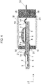
Fig. 4 is a cross-sectional view showing a mounting structure of a circuit board in which the housing is formed in the circuit module according to the first embodiment of the present invention. -
Fig. 5 is a view of a mounting structure of a circuit module according to a second embodiment of the present invention. -
Fig. 6 is a cross-sectional view taken along line A-A ofFig. 5 with respect to the circuit module according to the second embodiment of the present invention. -
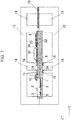
Fig. 7 is a cross-sectional view showing a mold structure for forming a housing in the circuit module to secure the circuit module according to the second embodiment of the present invention. -
Fig. 8 is a view of a mounting structure of a circuit module according to a third embodiment of the present invention. -
Fig. 9 is a cross-sectional view taken along line A-A ofFig. 8 with respect to the circuit module according to the third embodiment of the present invention. -
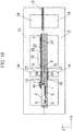
Fig. 10 is a cross-sectional view showing a mold structure for forming a housing in the circuit module to secure the circuit module according to the third embodiment of the present invention. -
Fig. 11 is a cross-sectional view of a mounting structure of the circuit board in which the housing is formed in the circuit module according to the third embodiment of the present invention. -
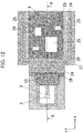
Fig. 12 is a view of a mounting structure of a circuit module according to a fourth embodiment of the present invention. -
Fig. 13 is a cross-sectional view taken along line A-A ofFig. 12 with respect to the circuit module according to the fourth embodiment of the present invention. -
Fig. 14 is a cross-sectional view showing a mold structure for forming a housing in the circuit module to secure the circuit module according to the fourth embodiment of the present invention. -
Fig. 15 is a cross-sectional view showing a mounting structure of the circuit board in which the housing is formed in the circuit module according to the fourth embodiment of the present invention. Description of Embodiments - Currently, the internal combustion engine of a car or vehicle is provided with modules including an electronic circuit, such as a sensor, an engine control unit, and an electronic control throttle. For these modules, a circuit board on which semiconductor parts are mounted is used. The circuit board is accommodated within a housing. In the conventional approach, the circuit board on which the semiconductor parts are mounted has been secured to a plastic housing by bonding with an adhesive. However, this method requires a process of applying and curing the adhesive, which reduces the throughput of the module manufacturing process. Thus, there is also another method called insert molding.
- Insert molding is the method of placing a circuit board within a mold in such a way that the circuit board is secured by pouring resin around the perimeter of the circuit board to form a plastic housing. In the method of insert molding, melting resin is directly brought into contact with the circuit board, so that the circuit board can be bonded to the housing simultaneously when the resin is solidified. In this way, it is possible to simplify the bonding process. Here, when the housing resin is brought into contact with the semiconductor parts on the circuit board, a load due to shrinkage of the resin can be easily applied to the semiconductor as well as the joint portion of the semiconductor parts and the circuit board. For this reason, the housing should be formed by pouring resin in such a way that the mounting area of the semiconductor parts is enclosed by the mold so that the mounting area and the peripheral board are not covered with the resin. However, this method blocks the resin by pressing the mold against the board. Thus, there is a risk that the board may be deformed by stress from the mold and deformation and crack may occur in the board.
- In the following embodiment, as an example of the insert molding using a board, an intake air flow sensor is described which is mounted on the internal combustion engine of a car. The intake air flow sensor is the flow sensor for measuring the flow rate of gas (air), which is provided to help control the intake air flow by an electronic fuel injector that is mounted on the internal combustion engine. The intake air flow sensor uses a sensor chip with a thin-walled diaphragm, in which the data measured by the sensor chip is collected and adjusted by a control chip and is output to the outside.
- Hereinafter, the first embodiment will be described with reference to the drawings.
-
Fig. 1 shows a circuit module mounted with a semiconductor chip having a control circuit and the like.Fig. 2 is a cross-sectional view of the semiconductor chip taken along line A-A ofFig. 1 , showing the mounting structure of the circuit module. - In
Fig. 2 , the circuit module is mounted with afirst semiconductor chip 3 including adiaphragm 2 on a printedcircuit board 1 of a material which is, for example, a lamination of glass fiber and resin, as well as asecond semiconductor chip 4 including a control circuit. The printedcircuit board 1 and thefirst semiconductor chip 3 are attached with an adhesive 5. Further, the printedcircuit board 1 and thesecond semiconductor chip 4 are attached with asecond adhesive 6. Inside the printedcircuit board 1, aconductor wiring 8 and awire pad 9 for the conductor wiring are formed. Thefirst semiconductor chip 3 and thesecond conductor chip 4 are connected by awire 7, theconductive wiring 8, and thewire pad 9. Further, thesecond semiconductor chip 4 is connected to theconductor wiring 8 by thewire 7. Apotting 10 is provided in order to protect thewire 7. - For example, thermosetting resin such as epoxy resin and polyurethane resin, as well as thermoplastic resin such as polyimide and acrylic resin can be used for the
first adhesive 5 bonding the printedboard 1 to thefirst semiconductor chip 3, thesecond adhesive 6 bonding the printedcircuit board 1 to thesecond semiconductor chip 4, and thepotting 9 for the protection of thewire 7. At the same time, a filler such as glass or mica can be mixed in the resin. - With respect to the mounting structure of the circuit module described above, a manufacturing method for bonding the circuit module to the housing while the area where the semiconductor parts are mounted is exposed.
-
Fig. 3 shows the mold structure for molding the circuit module while exposing the area where the semiconductor parts are mounted. The mounted circuit module and aconnector lead 13 are placed into a mold including anupper mold 11 and alower mold 12, in which ahollow portion 14 is formed by clamping the circuit module by aclamp portion 15 of the mold. Then, aresin 16 is injected into thehollow portion 14. - Next, as shown in
Fig. 14 , thewire pad 9 of the circuit module is connected to theconnector lead 13 by awire 17. Further, in order to protect acircuit chamber 18 which is a space including thewire 17, anupper cover 19 and alower cover 20 are bonded to the top and bottom of thecircuit chamber 18, respectively. By the process described above, the circuit module and the housing are bonded together while the semiconductor parts on the circuit module are exposed, to complete the sensor module capable of outputting the detected signal from the circuit module to the outside. - Here, the problem of the conventional insert molding as well as the features of the present embodiment will be described. When the circuit module is insert molded, the printed
circuit board 1 should be clamped in theclamp portion 15 of the mold so that theresin 16 does not flow to the semiconductor parts. At this time, if the load of theclamp portion 15 is excessive, deformation will occur in the printedcircuit board 1. Further, if the thickness of the printedcircuit board 1 varies and increases in the manufacturing process, the deformation could be further increased. In the conventional approach, nothing is placed in the position of theclamp portion 15, and the molding resin is injected into the mold that is in direct contact with the printedcircuit board 1. In the present embodiment, as shown inFigs. 3 and4 , amember 21 with an elastic modulus smaller than the average elastic modulus of the printedcircuit board 1 is added to themold clamp portion 15 on the printedcircuit board 1. As shown inFig. 3 , the housing is formed by injecting theresin 17 into thehollow portion 14 while clamping the area where themember 21 of the circuit module by theclamp portion 15 using theupper mold 11 and thelower mold 12. At the same time, the circuit module and the housing are bonded together. - The elastic modulus herein is the proportionality constant E when Hooke's law stating that the stress in an elastic body and the deformation are proportional to each other is expressed such that "the stress σ is proportional to the deformation ε, i.e., σ=Eε.
- For example, it is desirable to compare the elastic modulus of the
member 21 with the elastic modulus of the printedcircuit board 1 at thetemperature 25 °C (room temperature). Further, the comparison of the elastic modulus can be performed between the elastic modulus of themember 21 and the elastic modulus of the base material of the printedcircuit board 1. - In the above description, the comparison of the elastic modulus is made between the
member 21 and the printedcircuit board 1, the principle of which is that themember 21 whose hardness is softer than that of the printedcircuit board 1 is used. The hardness herein can be compared with Vickers hardness, Micro Vickers hardness, Brinell hardness, or Rockwell hardness at room temperature. - For the
member 21, for example, thermosetting resin such as epoxy resin and polyurethane resin or thermoplastic resin such as polyimide and acrylic resin can be used as long as it satisfies the requirement described above. At the same time, a filler such as glass or mica can be mixed in the resin. - In this manner, it is possible to reduce the load applied by the mold to the circuit board by the
member 21 in the insert molding process. As a result, it is possible to reduce the occurrence of deformation in the printedcircuit board 1. - Next, a description is given of a case where a wiring protective resist is placed on the wiring in the printed
circuit board 1 of the first embodiment. - In
Fig. 5 , thewiring 8 embedded in the printedcircuit board 1 inFig. 1 is formed on the board, in which a wiring protective resist 23 is provided in order to protect thewiring 8. - The
member 21 can also be applied to the configuration of the circuit board shown inFig. 5 . In this case, it is possible to use the same material as the wiring protective resist 23 as long as it satisfies the requirement that the elastic modulus of themember 21 is lower than the elastic modulus of the circuit board. In this embodiment, themember 21 can be placed at one time in the installation process of the wiring protective resist 23. As a result, the bonding process can be simplified - The mounting structure of a circuit module of a third embodiment is shown in
Fig. 8 . The third embodiment significantly differs from the first and second embodiments in that amember 24, which corresponds to themember 21 in the first and second embodiments, is also added to the area of thejoint portion 27 shown inFigs. 8 to 11 . - In
Fig. 8 , athird semiconductor chip 25 is connected to thewire pad 9 by anouter lead 26 that is derived from thethird semiconductor chip 25. With respect to this mounting structure, insert modeling is performed in order to bond the circuit module to the housing while exposing the area where the semiconductor parts of the circuit module are mounted. Themember 24 is placed on the main surface of thecircuit board 1 in the area where thecircuit board 1 overlaps themold clamp portion 15 as well as the area including thejoint portion 27 of the circuit board and the resin. - According to this embodiment, there is no need to accurately place the
member 24 in the contact area of the mold, so that the placement of themember 25 is easy compared to the first and second embodiments. Thus, it is possible to improve deterioration of the yield. In addition, it is possible to reduce the thermal stress generated after molding due to the difference in the linear expansion coefficient between thecircuit board 1 and theresin 16 by placing themember 21 in thejoint portion 27. As a result, it is possible to reduce the deformation of the circuit board and to prevent separation of the joint portion. - The present embodiment illustrates a circuit board in which a
conductor wiring 22 is placed also in theclamp portion 15 and thejoint portion 27, to which the present invention is applied. - Like the second and third embodiments, the wiring protective resist 23 is placed in the area except the
wire pad 9 of theconductor wiring 22 and in thearea 28 where the conductor wiring is exposed. In addition, in the present embodiment, theconductor wiring 22 is also placed in thecramp portion 15 and thejoint portion 27. Further, themember 24 is also placed over theconductor wiring 22 that is placed in theclamp portion 15 and thejoint portion 27. - With respect to such a mounting structure, insert modeling is performed in order to bond the circuit module to the housing while exposing the
area 28 where the semiconductor parts of the circuit module are mounted. The procedure of the insert molding using the mold is the same as the procedure described in the first to third embodiments. According to this embodiment, since themember 24 is placed over a wide range like the third embodiment, there is no need to accurately place themember 24 in the contact area of the mold, so that the placement of themember 25 is easy compared to the first and second embodiments. Thus, it is possible to improve deterioration of the yield. In addition, it is possible to reduce the thermal stress generated after molding due to the difference in the linear extension coefficient between the printedcircuit board 1 and theresin 16. As a result, it is possible to reduce the deformation of the circuit board and to prevent separation of the joint portion. - The above description illustrates an example of the component in which the intake air flow sensor is insert molded. However, the present invention is not limited only to this example, and it can be used for any component in which a circuit board, especially, a printed circuit board is insert molded.
- The invention made by the present inventors has been concretely described based on the embodiments. However, it is needless to say that the present invention is not limited to the above embodiments and various modifications and alterations can be made within the scope of the present invention.
- 1··· printed circuit board, 2··· diaphragm , 3··· first semiconductor chip, 4··· second semiconductor chip, 5··· first adhesive, 6··· second adhesive, 7··· wire, 8··· conductor wiring, 9··· wire pad, 10··· potting, 11··· upper mold, 12··· lower mold, 13··· connector lead, 14··· hollow portion, 15··· clamp portion, 16··· resin, 17··· wire, 18··· circuit chamber, 19··· upper cover, 20··· lower cover, 21··· member, 22··· conductor wiring, 23··· wiring protective resist, 24··· member, 25··· third semiconductor chip, 26··· outer lead, 27··· joint portion, 28··· area where the conductor wiring is exposed
Claims (6)
- A structure of insert molded article comprising:a printed circuit board mounted with semiconductor parts, in which the area where the semiconductor parts on the printed circuit board are not mounted is covered with a first resin,wherein a second resin with an elastic modulus smaller than the elastic modulus of the material of the printed circuit board is placed on the outside of the area where the main surface of the printed circuit board overlaps the first resin.
- The structure of insert molded article according to Claim 1, wherein a sensor structure includes a semiconductor for flow sensing that is exposed and placed in the printed circuit board.
- The sensor structure according to Claim 1 or 2, wherein the second resin placed in the printed circuit board is brought into contact with the first resin.
- The sensor structure according to Claim 1 or 2, wherein the second resin placed in the printed circuit board is of the same material that is placed in the conductor wiring formed on the printed circuit board.
- The sensor structure according to Claim 1 or 2, wherein the second resin placed in the printed circuit board is placed in the area where the first resin overlaps the printed circuit board.
- A sensor comprising the structure of insert molded article according to Claim 1.
Applications Claiming Priority (2)
| Application Number | Priority Date | Filing Date | Title |
|---|---|---|---|
| JP2014154430 | 2014-07-30 | ||
| PCT/JP2015/067110 WO2016017299A1 (en) | 2014-07-30 | 2015-06-15 | Circuit board mounting structure and sensor using same |
Publications (3)
| Publication Number | Publication Date |
|---|---|
| EP3176543A1 true EP3176543A1 (en) | 2017-06-07 |
| EP3176543A4 EP3176543A4 (en) | 2018-03-21 |
| EP3176543B1 EP3176543B1 (en) | 2020-11-18 |
Family
ID=55217204
Family Applications (1)
| Application Number | Title | Priority Date | Filing Date |
|---|---|---|---|
| EP15827155.1A Active EP3176543B1 (en) | 2014-07-30 | 2015-06-15 | Circuit board mounting structure and sensor using same |
Country Status (5)
| Country | Link |
|---|---|
| US (1) | US10031006B2 (en) |
| EP (1) | EP3176543B1 (en) |
| JP (1) | JP6357535B2 (en) |
| CN (1) | CN106461439B (en) |
| WO (1) | WO2016017299A1 (en) |
Cited By (1)
| Publication number | Priority date | Publication date | Assignee | Title |
|---|---|---|---|---|
| US10217684B2 (en) | 2015-09-30 | 2019-02-26 | Hitachi Automotive Systems, Ltd. | Resin molding and sensor device |
Families Citing this family (12)
| Publication number | Priority date | Publication date | Assignee | Title |
|---|---|---|---|---|
| US9967984B1 (en) | 2015-01-14 | 2018-05-08 | Vlt, Inc. | Power adapter packaging |
| US10264664B1 (en) | 2015-06-04 | 2019-04-16 | Vlt, Inc. | Method of electrically interconnecting circuit assemblies |
| JP6453790B2 (en) * | 2016-02-24 | 2019-01-16 | 日立オートモティブシステムズ株式会社 | Physical quantity detection device |
| US11336167B1 (en) | 2016-04-05 | 2022-05-17 | Vicor Corporation | Delivering power to semiconductor loads |
| US10158357B1 (en) | 2016-04-05 | 2018-12-18 | Vlt, Inc. | Method and apparatus for delivering power to semiconductors |
| US10785871B1 (en) * | 2018-12-12 | 2020-09-22 | Vlt, Inc. | Panel molded electronic assemblies with integral terminals |
| US10903734B1 (en) | 2016-04-05 | 2021-01-26 | Vicor Corporation | Delivering power to semiconductor loads |
| JP6866121B2 (en) * | 2016-11-14 | 2021-04-28 | 日立Astemo株式会社 | Semiconductor module |
| JP6825594B2 (en) * | 2018-03-09 | 2021-02-03 | オムロン株式会社 | Electronic devices and their manufacturing methods |
| WO2019225073A1 (en) * | 2018-05-22 | 2019-11-28 | 日立オートモティブシステムズ株式会社 | Physical quantity detecting device |
| DE102020211142B4 (en) * | 2020-09-03 | 2022-08-18 | Vitesco Technologies GmbH | Gas sensor for a vehicle |
| CN112802776B (en) * | 2020-12-31 | 2023-10-20 | 苏州首肯机械有限公司 | Intelligent pressure control system and control method for servo semiconductor packaging press |
Family Cites Families (22)
| Publication number | Priority date | Publication date | Assignee | Title |
|---|---|---|---|---|
| JPH08236560A (en) | 1995-03-01 | 1996-09-13 | Hitachi Ltd | Semiconductor integrated circuit device and manufacturing method thereof |
| JP3587734B2 (en) | 1999-06-30 | 2004-11-10 | 株式会社日立製作所 | Thermal air flow sensor |
| JP4017480B2 (en) * | 2002-09-24 | 2007-12-05 | Towa株式会社 | Resin sealing mold |
| JP2006211468A (en) * | 2005-01-31 | 2006-08-10 | Sanyo Electric Co Ltd | Semiconductor sensor |
| JP4548199B2 (en) * | 2005-04-22 | 2010-09-22 | 株式会社デンソー | Method for manufacturing electronic circuit device |
| JP4830391B2 (en) * | 2005-07-29 | 2011-12-07 | 株式会社デンソー | Manufacturing method of sensor device and sensor device |
| JP4674529B2 (en) * | 2005-11-07 | 2011-04-20 | 株式会社デンソー | Humidity sensor device and manufacturing method thereof |
| JP4882732B2 (en) * | 2006-12-22 | 2012-02-22 | 株式会社デンソー | Semiconductor device |
| ITMI20072099A1 (en) * | 2007-10-30 | 2009-04-30 | St Microelectronics Srl | METHOD OF MANUFACTURE OF AN ELECTRONIC DEVICE INCLUDING MEMS ENCAPSED MOLDING DEVICES |
| JP5068150B2 (en) * | 2007-11-30 | 2012-11-07 | ジヤトコ株式会社 | Control board unit capable of electrical analysis |
| JP5212133B2 (en) | 2009-01-21 | 2013-06-19 | 株式会社デンソー | Flow type sensor |
| JP5208099B2 (en) * | 2009-12-11 | 2013-06-12 | 日立オートモティブシステムズ株式会社 | Flow sensor, method for manufacturing the same, and flow sensor module |
| JP5563917B2 (en) * | 2010-07-22 | 2014-07-30 | セミコンダクター・コンポーネンツ・インダストリーズ・リミテッド・ライアビリティ・カンパニー | Circuit device and manufacturing method thereof |
| WO2012049742A1 (en) * | 2010-10-13 | 2012-04-19 | 日立オートモティブシステムズ株式会社 | Flow sensor and production method therefor, and flow sensor module and production method therefor |
| JP5645693B2 (en) | 2011-02-09 | 2014-12-24 | 日立オートモティブシステムズ株式会社 | Air flow measurement device |
| JP5526065B2 (en) * | 2011-03-25 | 2014-06-18 | 日立オートモティブシステムズ株式会社 | Thermal sensor and manufacturing method thereof |
| DE112011105438B4 (en) * | 2011-07-13 | 2020-06-18 | Hitachi Automotive Systems, Ltd. | Flow meter |
| JP2013188997A (en) * | 2012-03-15 | 2013-09-26 | Toyota Motor Corp | Method for manufacturing resin sealing component |
| JP5965706B2 (en) * | 2012-04-12 | 2016-08-10 | 日立オートモティブシステムズ株式会社 | Manufacturing method of flow sensor |
| JP5675716B2 (en) * | 2012-06-29 | 2015-02-25 | 日立オートモティブシステムズ株式会社 | Thermal air flow sensor |
| JP6018903B2 (en) * | 2012-12-17 | 2016-11-02 | 日立オートモティブシステムズ株式会社 | Physical quantity sensor |
| JP5949667B2 (en) * | 2013-06-03 | 2016-07-13 | 株式会社デンソー | Mold package and manufacturing method thereof |
-
2015
- 2015-06-15 EP EP15827155.1A patent/EP3176543B1/en active Active
- 2015-06-15 CN CN201580031470.7A patent/CN106461439B/en active Active
- 2015-06-15 US US15/316,981 patent/US10031006B2/en active Active
- 2015-06-15 WO PCT/JP2015/067110 patent/WO2016017299A1/en not_active Ceased
- 2015-06-15 JP JP2016538207A patent/JP6357535B2/en active Active
Cited By (1)
| Publication number | Priority date | Publication date | Assignee | Title |
|---|---|---|---|---|
| US10217684B2 (en) | 2015-09-30 | 2019-02-26 | Hitachi Automotive Systems, Ltd. | Resin molding and sensor device |
Also Published As
| Publication number | Publication date |
|---|---|
| US10031006B2 (en) | 2018-07-24 |
| WO2016017299A1 (en) | 2016-02-04 |
| CN106461439A (en) | 2017-02-22 |
| JPWO2016017299A1 (en) | 2017-04-27 |
| CN106461439B (en) | 2019-08-16 |
| EP3176543B1 (en) | 2020-11-18 |
| US20170115144A1 (en) | 2017-04-27 |
| JP6357535B2 (en) | 2018-07-11 |
| EP3176543A4 (en) | 2018-03-21 |
Similar Documents
| Publication | Publication Date | Title |
|---|---|---|
| US10031006B2 (en) | Sensor including a printed circuit board with semiconductor parts having a first and second resin | |
| US7216546B2 (en) | Pressure sensor having integrated temperature sensor | |
| CN107615034B (en) | Device for sensing the pressure of a fluid medium and method for producing said device | |
| JP4281630B2 (en) | Manufacturing method of sensor device | |
| CN1323289C (en) | Pressure sensor housed in the housing | |
| EP3358313B1 (en) | Resin-molded body and sensor device | |
| CN104364614A (en) | Flow rate sensor and method for making same | |
| EP2090873A1 (en) | Integrated circuit package | |
| US20180274964A1 (en) | Physical quantity sensor subassembly and physical quantity measuring device | |
| CN110553760B (en) | Overmolded lead frame assembly for pressure sensing applications | |
| US20070263367A1 (en) | Electronic subassembly, electronic assembly, and method for producing an electronic assembly | |
| WO2016039019A1 (en) | Flow rate sensor | |
| EP3660476A1 (en) | Cost overmolded leadframe force sensor with multiple mounting positions | |
| JP6551080B2 (en) | Flow measuring device | |
| US9618415B2 (en) | Pressure sensor package | |
| US20160137488A1 (en) | Method and apparatus of making mems packages | |
| JP6370379B2 (en) | Semiconductor device, method for manufacturing the semiconductor device, and sensor using the semiconductor device | |
| JP2016006438A (en) | Semiconductor device and method of manufacturing the same, flow sensor, and humidity sensor | |
| WO2014136336A1 (en) | Sensor device | |
| JP5912069B2 (en) | Physical quantity sensor device and manufacturing method thereof | |
| JP2006194682A (en) | Temperature sensor integrated pressure sensor device | |
| JP2019086417A (en) | Pressure sensor | |
| TW201810449A (en) | Device comprising a carrier and a housing, and a method of manufacturing a device comprising the component | |
| WO2019021766A1 (en) | Semiconductor device and method for producing semiconductor device |
Legal Events
| Date | Code | Title | Description |
|---|---|---|---|
| STAA | Information on the status of an ep patent application or granted ep patent |
Free format text: STATUS: THE INTERNATIONAL PUBLICATION HAS BEEN MADE |
|
| 17P | Request for examination filed |
Effective date: 20170228 |
|
| AK | Designated contracting states |
Kind code of ref document: A1 Designated state(s): AL AT BE BG CH CY CZ DE DK EE ES FI FR GB GR HR HU IE IS IT LI LT LU LV MC MK MT NL NO PL PT RO RS SE SI SK SM TR |
|
| AX | Request for extension of the european patent |
Extension state: BA ME |
|
| PUAI | Public reference made under article 153(3) epc to a published international application that has entered the european phase |
Free format text: ORIGINAL CODE: 0009012 |
|
| STAA | Information on the status of an ep patent application or granted ep patent |
Free format text: STATUS: REQUEST FOR EXAMINATION WAS MADE |
|
| DAV | Request for validation of the european patent (deleted) | ||
| DAX | Request for extension of the european patent (deleted) | ||
| A4 | Supplementary search report drawn up and despatched |
Effective date: 20180220 |
|
| RIC1 | Information provided on ipc code assigned before grant |
Ipc: H01L 23/498 20060101ALI20180212BHEP Ipc: H05K 3/28 20060101ALI20180212BHEP Ipc: H05K 1/02 20060101ALI20180212BHEP Ipc: H01L 21/56 20060101ALI20180212BHEP Ipc: H05K 1/18 20060101ALI20180212BHEP Ipc: H01L 23/28 20060101ALI20180212BHEP Ipc: H01L 23/00 20060101ALI20180212BHEP Ipc: H01L 23/31 20060101ALI20180212BHEP Ipc: H01L 23/12 20060101ALI20180212BHEP Ipc: G01F 1/684 20060101AFI20180212BHEP Ipc: G01F 1/692 20060101ALI20180212BHEP |
|
| STAA | Information on the status of an ep patent application or granted ep patent |
Free format text: STATUS: EXAMINATION IS IN PROGRESS |
|
| 17Q | First examination report despatched |
Effective date: 20181015 |
|
| GRAP | Despatch of communication of intention to grant a patent |
Free format text: ORIGINAL CODE: EPIDOSNIGR1 |
|
| STAA | Information on the status of an ep patent application or granted ep patent |
Free format text: STATUS: GRANT OF PATENT IS INTENDED |
|
| INTG | Intention to grant announced |
Effective date: 20200713 |
|
| GRAS | Grant fee paid |
Free format text: ORIGINAL CODE: EPIDOSNIGR3 |
|
| GRAA | (expected) grant |
Free format text: ORIGINAL CODE: 0009210 |
|
| STAA | Information on the status of an ep patent application or granted ep patent |
Free format text: STATUS: THE PATENT HAS BEEN GRANTED |
|
| AK | Designated contracting states |
Kind code of ref document: B1 Designated state(s): AL AT BE BG CH CY CZ DE DK EE ES FI FR GB GR HR HU IE IS IT LI LT LU LV MC MK MT NL NO PL PT RO RS SE SI SK SM TR |
|
| REG | Reference to a national code |
Ref country code: GB Ref legal event code: FG4D |
|
| REG | Reference to a national code |
Ref country code: CH Ref legal event code: EP |
|
| REG | Reference to a national code |
Ref country code: IE Ref legal event code: FG4D |
|
| REG | Reference to a national code |
Ref country code: DE Ref legal event code: R096 Ref document number: 602015062292 Country of ref document: DE |
|
| REG | Reference to a national code |
Ref country code: AT Ref legal event code: REF Ref document number: 1336260 Country of ref document: AT Kind code of ref document: T Effective date: 20201215 |
|
| REG | Reference to a national code |
Ref country code: AT Ref legal event code: MK05 Ref document number: 1336260 Country of ref document: AT Kind code of ref document: T Effective date: 20201118 |
|
| REG | Reference to a national code |
Ref country code: NL Ref legal event code: MP Effective date: 20201118 |
|
| PG25 | Lapsed in a contracting state [announced via postgrant information from national office to epo] |
Ref country code: GR Free format text: LAPSE BECAUSE OF FAILURE TO SUBMIT A TRANSLATION OF THE DESCRIPTION OR TO PAY THE FEE WITHIN THE PRESCRIBED TIME-LIMIT Effective date: 20210219 Ref country code: NO Free format text: LAPSE BECAUSE OF FAILURE TO SUBMIT A TRANSLATION OF THE DESCRIPTION OR TO PAY THE FEE WITHIN THE PRESCRIBED TIME-LIMIT Effective date: 20210218 Ref country code: RS Free format text: LAPSE BECAUSE OF FAILURE TO SUBMIT A TRANSLATION OF THE DESCRIPTION OR TO PAY THE FEE WITHIN THE PRESCRIBED TIME-LIMIT Effective date: 20201118 Ref country code: PT Free format text: LAPSE BECAUSE OF FAILURE TO SUBMIT A TRANSLATION OF THE DESCRIPTION OR TO PAY THE FEE WITHIN THE PRESCRIBED TIME-LIMIT Effective date: 20210318 Ref country code: FI Free format text: LAPSE BECAUSE OF FAILURE TO SUBMIT A TRANSLATION OF THE DESCRIPTION OR TO PAY THE FEE WITHIN THE PRESCRIBED TIME-LIMIT Effective date: 20201118 |
|
| PG25 | Lapsed in a contracting state [announced via postgrant information from national office to epo] |
Ref country code: BG Free format text: LAPSE BECAUSE OF FAILURE TO SUBMIT A TRANSLATION OF THE DESCRIPTION OR TO PAY THE FEE WITHIN THE PRESCRIBED TIME-LIMIT Effective date: 20210218 Ref country code: AT Free format text: LAPSE BECAUSE OF FAILURE TO SUBMIT A TRANSLATION OF THE DESCRIPTION OR TO PAY THE FEE WITHIN THE PRESCRIBED TIME-LIMIT Effective date: 20201118 Ref country code: LV Free format text: LAPSE BECAUSE OF FAILURE TO SUBMIT A TRANSLATION OF THE DESCRIPTION OR TO PAY THE FEE WITHIN THE PRESCRIBED TIME-LIMIT Effective date: 20201118 Ref country code: IS Free format text: LAPSE BECAUSE OF FAILURE TO SUBMIT A TRANSLATION OF THE DESCRIPTION OR TO PAY THE FEE WITHIN THE PRESCRIBED TIME-LIMIT Effective date: 20210318 Ref country code: SE Free format text: LAPSE BECAUSE OF FAILURE TO SUBMIT A TRANSLATION OF THE DESCRIPTION OR TO PAY THE FEE WITHIN THE PRESCRIBED TIME-LIMIT Effective date: 20201118 Ref country code: PL Free format text: LAPSE BECAUSE OF FAILURE TO SUBMIT A TRANSLATION OF THE DESCRIPTION OR TO PAY THE FEE WITHIN THE PRESCRIBED TIME-LIMIT Effective date: 20201118 |
|
| REG | Reference to a national code |
Ref country code: LT Ref legal event code: MG9D |
|
| PG25 | Lapsed in a contracting state [announced via postgrant information from national office to epo] |
Ref country code: HR Free format text: LAPSE BECAUSE OF FAILURE TO SUBMIT A TRANSLATION OF THE DESCRIPTION OR TO PAY THE FEE WITHIN THE PRESCRIBED TIME-LIMIT Effective date: 20201118 |
|
| PG25 | Lapsed in a contracting state [announced via postgrant information from national office to epo] |
Ref country code: LT Free format text: LAPSE BECAUSE OF FAILURE TO SUBMIT A TRANSLATION OF THE DESCRIPTION OR TO PAY THE FEE WITHIN THE PRESCRIBED TIME-LIMIT Effective date: 20201118 Ref country code: SK Free format text: LAPSE BECAUSE OF FAILURE TO SUBMIT A TRANSLATION OF THE DESCRIPTION OR TO PAY THE FEE WITHIN THE PRESCRIBED TIME-LIMIT Effective date: 20201118 Ref country code: RO Free format text: LAPSE BECAUSE OF FAILURE TO SUBMIT A TRANSLATION OF THE DESCRIPTION OR TO PAY THE FEE WITHIN THE PRESCRIBED TIME-LIMIT Effective date: 20201118 Ref country code: CZ Free format text: LAPSE BECAUSE OF FAILURE TO SUBMIT A TRANSLATION OF THE DESCRIPTION OR TO PAY THE FEE WITHIN THE PRESCRIBED TIME-LIMIT Effective date: 20201118 Ref country code: EE Free format text: LAPSE BECAUSE OF FAILURE TO SUBMIT A TRANSLATION OF THE DESCRIPTION OR TO PAY THE FEE WITHIN THE PRESCRIBED TIME-LIMIT Effective date: 20201118 Ref country code: SM Free format text: LAPSE BECAUSE OF FAILURE TO SUBMIT A TRANSLATION OF THE DESCRIPTION OR TO PAY THE FEE WITHIN THE PRESCRIBED TIME-LIMIT Effective date: 20201118 |
|
| REG | Reference to a national code |
Ref country code: DE Ref legal event code: R097 Ref document number: 602015062292 Country of ref document: DE |
|
| PG25 | Lapsed in a contracting state [announced via postgrant information from national office to epo] |
Ref country code: DK Free format text: LAPSE BECAUSE OF FAILURE TO SUBMIT A TRANSLATION OF THE DESCRIPTION OR TO PAY THE FEE WITHIN THE PRESCRIBED TIME-LIMIT Effective date: 20201118 |
|
| REG | Reference to a national code |
Ref country code: DE Ref legal event code: R081 Ref document number: 602015062292 Country of ref document: DE Owner name: HITACHI ASTEMO, LTD., HITACHINAKA-SHI, JP Free format text: FORMER OWNER: HITACHI AUTOMOTIVE SYSTEMS, LTD., HITACHINAKA-SHI, IBARAKI, JP |
|
| PLBE | No opposition filed within time limit |
Free format text: ORIGINAL CODE: 0009261 |
|
| STAA | Information on the status of an ep patent application or granted ep patent |
Free format text: STATUS: NO OPPOSITION FILED WITHIN TIME LIMIT |
|
| 26N | No opposition filed |
Effective date: 20210819 |
|
| PG25 | Lapsed in a contracting state [announced via postgrant information from national office to epo] |
Ref country code: NL Free format text: LAPSE BECAUSE OF FAILURE TO SUBMIT A TRANSLATION OF THE DESCRIPTION OR TO PAY THE FEE WITHIN THE PRESCRIBED TIME-LIMIT Effective date: 20201118 Ref country code: IT Free format text: LAPSE BECAUSE OF FAILURE TO SUBMIT A TRANSLATION OF THE DESCRIPTION OR TO PAY THE FEE WITHIN THE PRESCRIBED TIME-LIMIT Effective date: 20201118 Ref country code: AL Free format text: LAPSE BECAUSE OF FAILURE TO SUBMIT A TRANSLATION OF THE DESCRIPTION OR TO PAY THE FEE WITHIN THE PRESCRIBED TIME-LIMIT Effective date: 20201118 |
|
| PG25 | Lapsed in a contracting state [announced via postgrant information from national office to epo] |
Ref country code: SI Free format text: LAPSE BECAUSE OF FAILURE TO SUBMIT A TRANSLATION OF THE DESCRIPTION OR TO PAY THE FEE WITHIN THE PRESCRIBED TIME-LIMIT Effective date: 20201118 |
|
| PG25 | Lapsed in a contracting state [announced via postgrant information from national office to epo] |
Ref country code: ES Free format text: LAPSE BECAUSE OF FAILURE TO SUBMIT A TRANSLATION OF THE DESCRIPTION OR TO PAY THE FEE WITHIN THE PRESCRIBED TIME-LIMIT Effective date: 20201118 Ref country code: MC Free format text: LAPSE BECAUSE OF FAILURE TO SUBMIT A TRANSLATION OF THE DESCRIPTION OR TO PAY THE FEE WITHIN THE PRESCRIBED TIME-LIMIT Effective date: 20201118 |
|
| REG | Reference to a national code |
Ref country code: CH Ref legal event code: PL |
|
| GBPC | Gb: european patent ceased through non-payment of renewal fee |
Effective date: 20210615 |
|
| REG | Reference to a national code |
Ref country code: BE Ref legal event code: MM Effective date: 20210630 |
|
| PG25 | Lapsed in a contracting state [announced via postgrant information from national office to epo] |
Ref country code: LU Free format text: LAPSE BECAUSE OF NON-PAYMENT OF DUE FEES Effective date: 20210615 |
|
| PG25 | Lapsed in a contracting state [announced via postgrant information from national office to epo] |
Ref country code: LI Free format text: LAPSE BECAUSE OF NON-PAYMENT OF DUE FEES Effective date: 20210630 Ref country code: IE Free format text: LAPSE BECAUSE OF NON-PAYMENT OF DUE FEES Effective date: 20210615 Ref country code: GB Free format text: LAPSE BECAUSE OF NON-PAYMENT OF DUE FEES Effective date: 20210615 Ref country code: CH Free format text: LAPSE BECAUSE OF NON-PAYMENT OF DUE FEES Effective date: 20210630 |
|
| PG25 | Lapsed in a contracting state [announced via postgrant information from national office to epo] |
Ref country code: IS Free format text: LAPSE BECAUSE OF FAILURE TO SUBMIT A TRANSLATION OF THE DESCRIPTION OR TO PAY THE FEE WITHIN THE PRESCRIBED TIME-LIMIT Effective date: 20210318 Ref country code: FR Free format text: LAPSE BECAUSE OF NON-PAYMENT OF DUE FEES Effective date: 20210630 |
|
| PG25 | Lapsed in a contracting state [announced via postgrant information from national office to epo] |
Ref country code: BE Free format text: LAPSE BECAUSE OF NON-PAYMENT OF DUE FEES Effective date: 20210630 |
|
| PG25 | Lapsed in a contracting state [announced via postgrant information from national office to epo] |
Ref country code: HU Free format text: LAPSE BECAUSE OF FAILURE TO SUBMIT A TRANSLATION OF THE DESCRIPTION OR TO PAY THE FEE WITHIN THE PRESCRIBED TIME-LIMIT; INVALID AB INITIO Effective date: 20150615 |
|
| PG25 | Lapsed in a contracting state [announced via postgrant information from national office to epo] |
Ref country code: CY Free format text: LAPSE BECAUSE OF FAILURE TO SUBMIT A TRANSLATION OF THE DESCRIPTION OR TO PAY THE FEE WITHIN THE PRESCRIBED TIME-LIMIT Effective date: 20201118 |
|
| PG25 | Lapsed in a contracting state [announced via postgrant information from national office to epo] |
Ref country code: MK Free format text: LAPSE BECAUSE OF FAILURE TO SUBMIT A TRANSLATION OF THE DESCRIPTION OR TO PAY THE FEE WITHIN THE PRESCRIBED TIME-LIMIT Effective date: 20201118 |
|
| PG25 | Lapsed in a contracting state [announced via postgrant information from national office to epo] |
Ref country code: TR Free format text: LAPSE BECAUSE OF FAILURE TO SUBMIT A TRANSLATION OF THE DESCRIPTION OR TO PAY THE FEE WITHIN THE PRESCRIBED TIME-LIMIT Effective date: 20201118 |
|
| PG25 | Lapsed in a contracting state [announced via postgrant information from national office to epo] |
Ref country code: MT Free format text: LAPSE BECAUSE OF FAILURE TO SUBMIT A TRANSLATION OF THE DESCRIPTION OR TO PAY THE FEE WITHIN THE PRESCRIBED TIME-LIMIT Effective date: 20201118 |
|
| PGFP | Annual fee paid to national office [announced via postgrant information from national office to epo] |
Ref country code: DE Payment date: 20260430 Year of fee payment: 12 |