EP3174120A1 - Organic light-emitting display device - Google Patents
Organic light-emitting display device Download PDFInfo
- Publication number
- EP3174120A1 EP3174120A1 EP16198400.0A EP16198400A EP3174120A1 EP 3174120 A1 EP3174120 A1 EP 3174120A1 EP 16198400 A EP16198400 A EP 16198400A EP 3174120 A1 EP3174120 A1 EP 3174120A1
- Authority
- EP
- European Patent Office
- Prior art keywords
- organic light
- layer
- emitting display
- passivation layer
- display device
- Prior art date
- Legal status (The legal status is an assumption and is not a legal conclusion. Google has not performed a legal analysis and makes no representation as to the accuracy of the status listed.)
- Granted
Links
Images



Classifications
-
- H—ELECTRICITY
- H10—SEMICONDUCTOR DEVICES; ELECTRIC SOLID-STATE DEVICES NOT OTHERWISE PROVIDED FOR
- H10K—ORGANIC ELECTRIC SOLID-STATE DEVICES
- H10K59/00—Integrated devices, or assemblies of multiple devices, comprising at least one organic light-emitting element covered by group H10K50/00
- H10K59/80—Constructional details
- H10K59/87—Passivation; Containers; Encapsulations
- H10K59/871—Self-supporting sealing arrangements
-
- H—ELECTRICITY
- H10—SEMICONDUCTOR DEVICES; ELECTRIC SOLID-STATE DEVICES NOT OTHERWISE PROVIDED FOR
- H10D—INORGANIC ELECTRIC SEMICONDUCTOR DEVICES
- H10D30/00—Field-effect transistors [FET]
- H10D30/60—Insulated-gate field-effect transistors [IGFET]
- H10D30/67—Thin-film transistors [TFT]
- H10D30/674—Thin-film transistors [TFT] characterised by the active materials
- H10D30/6755—Oxide semiconductors, e.g. zinc oxide, copper aluminium oxide or cadmium stannate
-
- H—ELECTRICITY
- H10—SEMICONDUCTOR DEVICES; ELECTRIC SOLID-STATE DEVICES NOT OTHERWISE PROVIDED FOR
- H10K—ORGANIC ELECTRIC SOLID-STATE DEVICES
- H10K50/00—Organic light-emitting devices
- H10K50/80—Constructional details
- H10K50/84—Passivation; Containers; Encapsulations
- H10K50/841—Self-supporting sealing arrangements
-
- H—ELECTRICITY
- H10—SEMICONDUCTOR DEVICES; ELECTRIC SOLID-STATE DEVICES NOT OTHERWISE PROVIDED FOR
- H10K—ORGANIC ELECTRIC SOLID-STATE DEVICES
- H10K50/00—Organic light-emitting devices
- H10K50/80—Constructional details
- H10K50/84—Passivation; Containers; Encapsulations
- H10K50/842—Containers
- H10K50/8426—Peripheral sealing arrangements, e.g. adhesives, sealants
-
- H—ELECTRICITY
- H10—SEMICONDUCTOR DEVICES; ELECTRIC SOLID-STATE DEVICES NOT OTHERWISE PROVIDED FOR
- H10K—ORGANIC ELECTRIC SOLID-STATE DEVICES
- H10K50/00—Organic light-emitting devices
- H10K50/80—Constructional details
- H10K50/84—Passivation; Containers; Encapsulations
- H10K50/844—Encapsulations
-
- H—ELECTRICITY
- H10—SEMICONDUCTOR DEVICES; ELECTRIC SOLID-STATE DEVICES NOT OTHERWISE PROVIDED FOR
- H10K—ORGANIC ELECTRIC SOLID-STATE DEVICES
- H10K59/00—Integrated devices, or assemblies of multiple devices, comprising at least one organic light-emitting element covered by group H10K50/00
- H10K59/10—OLED displays
- H10K59/12—Active-matrix OLED [AMOLED] displays
- H10K59/121—Active-matrix OLED [AMOLED] displays characterised by the geometry or disposition of pixel elements
- H10K59/1213—Active-matrix OLED [AMOLED] displays characterised by the geometry or disposition of pixel elements the pixel elements being TFTs
-
- H—ELECTRICITY
- H10—SEMICONDUCTOR DEVICES; ELECTRIC SOLID-STATE DEVICES NOT OTHERWISE PROVIDED FOR
- H10K—ORGANIC ELECTRIC SOLID-STATE DEVICES
- H10K59/00—Integrated devices, or assemblies of multiple devices, comprising at least one organic light-emitting element covered by group H10K50/00
- H10K59/30—Devices specially adapted for multicolour light emission
- H10K59/38—Devices specially adapted for multicolour light emission comprising colour filters or colour changing media [CCM]
-
- H—ELECTRICITY
- H10—SEMICONDUCTOR DEVICES; ELECTRIC SOLID-STATE DEVICES NOT OTHERWISE PROVIDED FOR
- H10K—ORGANIC ELECTRIC SOLID-STATE DEVICES
- H10K59/00—Integrated devices, or assemblies of multiple devices, comprising at least one organic light-emitting element covered by group H10K50/00
- H10K59/80—Constructional details
- H10K59/87—Passivation; Containers; Encapsulations
- H10K59/871—Self-supporting sealing arrangements
- H10K59/8722—Peripheral sealing arrangements, e.g. adhesives, sealants
-
- H—ELECTRICITY
- H10—SEMICONDUCTOR DEVICES; ELECTRIC SOLID-STATE DEVICES NOT OTHERWISE PROVIDED FOR
- H10K—ORGANIC ELECTRIC SOLID-STATE DEVICES
- H10K59/00—Integrated devices, or assemblies of multiple devices, comprising at least one organic light-emitting element covered by group H10K50/00
- H10K59/80—Constructional details
- H10K59/87—Passivation; Containers; Encapsulations
- H10K59/873—Encapsulations
-
- H—ELECTRICITY
- H10—SEMICONDUCTOR DEVICES; ELECTRIC SOLID-STATE DEVICES NOT OTHERWISE PROVIDED FOR
- H10D—INORGANIC ELECTRIC SEMICONDUCTOR DEVICES
- H10D30/00—Field-effect transistors [FET]
- H10D30/60—Insulated-gate field-effect transistors [IGFET]
- H10D30/67—Thin-film transistors [TFT]
- H10D30/6704—Thin-film transistors [TFT] having supplementary regions or layers in the thin films or in the insulated bulk substrates for controlling properties of the device
-
- H—ELECTRICITY
- H10—SEMICONDUCTOR DEVICES; ELECTRIC SOLID-STATE DEVICES NOT OTHERWISE PROVIDED FOR
- H10D—INORGANIC ELECTRIC SEMICONDUCTOR DEVICES
- H10D86/00—Integrated devices formed in or on insulating or conducting substrates, e.g. formed in silicon-on-insulator [SOI] substrates or on stainless steel or glass substrates
- H10D86/40—Integrated devices formed in or on insulating or conducting substrates, e.g. formed in silicon-on-insulator [SOI] substrates or on stainless steel or glass substrates characterised by multiple TFTs
- H10D86/421—Integrated devices formed in or on insulating or conducting substrates, e.g. formed in silicon-on-insulator [SOI] substrates or on stainless steel or glass substrates characterised by multiple TFTs having a particular composition, shape or crystalline structure of the active layer
- H10D86/423—Integrated devices formed in or on insulating or conducting substrates, e.g. formed in silicon-on-insulator [SOI] substrates or on stainless steel or glass substrates characterised by multiple TFTs having a particular composition, shape or crystalline structure of the active layer comprising semiconductor materials not belonging to the Group IV, e.g. InGaZnO
-
- H—ELECTRICITY
- H10—SEMICONDUCTOR DEVICES; ELECTRIC SOLID-STATE DEVICES NOT OTHERWISE PROVIDED FOR
- H10D—INORGANIC ELECTRIC SEMICONDUCTOR DEVICES
- H10D86/00—Integrated devices formed in or on insulating or conducting substrates, e.g. formed in silicon-on-insulator [SOI] substrates or on stainless steel or glass substrates
- H10D86/40—Integrated devices formed in or on insulating or conducting substrates, e.g. formed in silicon-on-insulator [SOI] substrates or on stainless steel or glass substrates characterised by multiple TFTs
- H10D86/60—Integrated devices formed in or on insulating or conducting substrates, e.g. formed in silicon-on-insulator [SOI] substrates or on stainless steel or glass substrates characterised by multiple TFTs wherein the TFTs are in active matrices
-
- H—ELECTRICITY
- H10—SEMICONDUCTOR DEVICES; ELECTRIC SOLID-STATE DEVICES NOT OTHERWISE PROVIDED FOR
- H10K—ORGANIC ELECTRIC SOLID-STATE DEVICES
- H10K2102/00—Constructional details relating to the organic devices covered by this subclass
-
- H—ELECTRICITY
- H10—SEMICONDUCTOR DEVICES; ELECTRIC SOLID-STATE DEVICES NOT OTHERWISE PROVIDED FOR
- H10K—ORGANIC ELECTRIC SOLID-STATE DEVICES
- H10K50/00—Organic light-emitting devices
- H10K50/80—Constructional details
- H10K50/84—Passivation; Containers; Encapsulations
-
- H—ELECTRICITY
- H10—SEMICONDUCTOR DEVICES; ELECTRIC SOLID-STATE DEVICES NOT OTHERWISE PROVIDED FOR
- H10K—ORGANIC ELECTRIC SOLID-STATE DEVICES
- H10K50/00—Organic light-emitting devices
- H10K50/80—Constructional details
- H10K50/84—Passivation; Containers; Encapsulations
- H10K50/846—Passivation; Containers; Encapsulations comprising getter material or desiccants
-
- H—ELECTRICITY
- H10—SEMICONDUCTOR DEVICES; ELECTRIC SOLID-STATE DEVICES NOT OTHERWISE PROVIDED FOR
- H10K—ORGANIC ELECTRIC SOLID-STATE DEVICES
- H10K59/00—Integrated devices, or assemblies of multiple devices, comprising at least one organic light-emitting element covered by group H10K50/00
- H10K59/10—OLED displays
- H10K59/12—Active-matrix OLED [AMOLED] displays
-
- H—ELECTRICITY
- H10—SEMICONDUCTOR DEVICES; ELECTRIC SOLID-STATE DEVICES NOT OTHERWISE PROVIDED FOR
- H10K—ORGANIC ELECTRIC SOLID-STATE DEVICES
- H10K59/00—Integrated devices, or assemblies of multiple devices, comprising at least one organic light-emitting element covered by group H10K50/00
- H10K59/80—Constructional details
- H10K59/87—Passivation; Containers; Encapsulations
- H10K59/874—Passivation; Containers; Encapsulations including getter material or desiccant
-
- Y—GENERAL TAGGING OF NEW TECHNOLOGICAL DEVELOPMENTS; GENERAL TAGGING OF CROSS-SECTIONAL TECHNOLOGIES SPANNING OVER SEVERAL SECTIONS OF THE IPC; TECHNICAL SUBJECTS COVERED BY FORMER USPC CROSS-REFERENCE ART COLLECTIONS [XRACs] AND DIGESTS
- Y02—TECHNOLOGIES OR APPLICATIONS FOR MITIGATION OR ADAPTATION AGAINST CLIMATE CHANGE
- Y02E—REDUCTION OF GREENHOUSE GAS [GHG] EMISSIONS, RELATED TO ENERGY GENERATION, TRANSMISSION OR DISTRIBUTION
- Y02E10/00—Energy generation through renewable energy sources
- Y02E10/50—Photovoltaic [PV] energy
- Y02E10/549—Organic PV cells
Definitions
- the present disclosure relates to an organic light-emitting display (OLED) device and an encapsulation structure.
- OLED organic light-emitting display
- Display devices provide a variety of information graphically on a screen and are the core technology of information communications. Such display devices are becoming thinner, lighter and easier to carry, along with higher performance. With such trend, organic light-emitting display (OLED) devices are attracting attention, which control the amount of light emitted from an organic emission layer to display images.
- OLED organic light-emitting display
- An OLED device is a self-luminous device using a thin emission layer between electrodes, and thus the overall device can be made thinner. Further, an OLED device is not only advantageous in terms of power consumption by low voltage driving, and also has excellent color implementation, response speed, viewing angle and contrast ratio (CR).
- a pixel drive circuit and an organic light-emitting element are formed on a substrate, and light emitted from an organic light-emitting element may pass the substrate or a barrier layer, thereby displaying images.
- the organic light-emitting element can easily deteriorate by internal factors such as deterioration of the electrodes and the emission layer due to oxygen or moisture, deterioration by the reaction between the emission layer and interface, etc., as well as external factors such as moisture, oxygen, ultraviolet rays and processing limitations of the device. Among these, oxygen and moisture seriously affect the lifespan of the OLED device, and thus encapsulation of the OLED device is very important.
- the encapsulation techniques there is a known method of sealing the space above an organic light-emitting element with a passivation layer, or proving a face seal, or employing an encapsulation plate.
- the face seal contains moisture absorbent material to absorb moisture permeating into the organic light-emitting element.
- the face seal is applied on the inner surface of the encapsulation plate, and then the encapsulation plate is attached to a pixel array substrate. After the face seal sandwiched between the two substrate attached together (the encapsulation plate and the pixel array substrate) has been cured, pressure exerted against the substrates is removed, such that an OLED device having the face seal structure is fabricated.
- the encapsulation plate may be made of glass, plastic, metal or the like.
- an object of the present disclosure is to provide an OLED device and an improved encapsulation structure used therein. Another object of the present disclosure is to provide an organic element passivation layer with improved reliability.
- an OLED device including: a pixel drive circuit and organic light-emitting element on an array substrate; a passivation layer covering the pixel drive circuit and organic light-emitting element so as to block permeation of moisture; and an adhesive layer on the passivation layer.
- the passivation layer is an inorganic thin film based on an organosilicon compound.
- a change in characteristics of a TFT due to hydrogen permeation can be reduced.
- bright spots are reduced, such that the reliability of an OLED device can be improved.
- phrases such as first, second, A, B, (a), (b), etc. may be used. These terms are used only to differentiate a component from another component. Therefore, the nature, sequence, order, number, etc., of the components are not limited by these terms.
- phrases "an element A connected to an element B" or “an element A coupled with an element B” refer to that the element A may be directly connected to/coupled with the element B, that that another element C may be interposed between the element A and the element B, and/or that the element A may be indirectly connected to/coupled with the element B via another element C.
- an element A on an element B refers to that the element A may be disposed directly on the element B and/or the element A may be disposed indirectly on the element B via another element C.
- the drawings are not to scale and the relative dimensions of various elements in the drawings are depicted schematically and not necessarily to scale.
- OLED device or “display device” collectively refers to an organic light-emitting diode panel and a display device employing such an organic light-emitting diode panel.
- OLED devices may be divided into white organic light-emitting display devices and RGB organic light-emitting display devices.
- a white organic light-emitting device sub-pixels in each of pixels emits white light, and a set of color filters is used in each of the sub-pixels to filter white light to produce red light, green light or blue light.
- a white organic light-emitting device may include sub-pixels with no color filter for forming sub-pixels for producing white light.
- an organic emission layer is configured to emit light of a particular color in each of sub-pixels.
- a single pixel includes a red sub-pixel having an organic emission layer for emitting red light, a green sub-pixel having an organic emission layer for emitting green light, and a blue sub-pixel having an organic emission layer for emitting blue light.
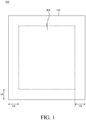
- FIG. 1 is a plan view of an organic light-emitting display (OLED) device according to an exemplary embodiment of the present disclosure.
- an OLED device 100 includes at least one active area A/A, in which an array of pixels is disposed.
- One or more inactive areas I/A may be disposed around the active area. That is, the inactive areas may be adjacent to one or more sides of the active area. In FIG. 1 , the inactive areas surround a rectangular active area.
- the shape of the active area and the shape/layout of the inactive areas adjacent to the active area are not limited to those shown in FIG. 1 .
- the active area and the inactive areas may have shapes appropriate for the design of an electronic device employing the display device 100.
- the active area may have a pentagon shape, a hexagon shape, a circle shape, an ellipse shape, etc.
- Each of the pixels in the active area may be electrically connected to corresponding pixel drive circuits.
- Each of the pixel drive circuits may include at least one switching transistor and at least one driving transistor.
- Each of the pixel drive circuits may be electrically connected to gate lines and data lines so as to transfer signals with a gate driver, a data driver, etc., disposed in the inactive area.
- the gate driver and the data driver may be implemented with thin-film transistors (TFTs) in the inactive area.
- the drivers may be referred to GIP circuits (gate-in-panel) circuits.
- some components such as a data driver IC (integrated circuit) may be mounted on a separated PCB (printed circuit board) and may be coupled with a connection interface (a pad, a bump, a pin, etc.) disposed in the inactive area via a circuit film such as a FPCB (flexible printed circuit board), a COF (chip-on-film), a TCP (tape-carrier-package), etc.
- the printed circuits (COF, PCB, etc.) may be disposed behind the display device 100 upon being folded over to a rear thereof.
- the OLED device 100 may include a variety of additional elements for generating various signals or voltages for driving the pixels in the active area.
- the additional elements for driving the pixels may include an inverter circuit, a multiplexer, an electro static discharge circuit, etc.
- the OLED device 100 may include elements associated with features other than driving the pixels.
- the OLED device 100 may include additional elements for providing a touch sense feature, a user authentication feature (e.g., fingerprint recognition), a multi-level pressure sense feature, a tactile feedback feature, etc. At least some of the above-mentioned additional elements may be disposed in the inactive areas and/or an external circuit connected to the connection interface.
- the OLED device may include a thin-film transistor and an organic light-emitting element on an array substrate 110, an encapsulation layer on the organic light-emitting element, a barrier film attaching the substrate to the encapsulation layer, and the like.
- array substrate 110 may also refer to the substrate itself as well as elements and functional layers formed thereon, e.g., a switching TFT, a driving TFT connected to the switching TFT, an organic light-emitting element connected to the driving TFT, a protective film, etc.
- the array substrate 110 supports a variety of elements of the OLED device 100 and is made of an insulative material.
- the array substrate 110 may be made of a transparent, insulative material such as glass, plastic, etc.
- the organic light-emitting element is disposed on the array substrate 110.
- the organic light-emitting element includes an anode, an organic emission layer formed on the anode, and a cathode formed on the organic emission layer.
- the organic emission layer may be made up of a single emission layer emitting light of a color or may be made up of a plurality of emission layers to emit white light.
- the organic light-emitting element may be formed in the center of the array substrate 110 such that it is located in the active area. In the case that the organic emission layer of the organic light-emitting element emits white light, color filters may be further disposed.
- the passivation layer may cover the organic light-emitting element.
- the passivation layer protects the organic light-emitting element from moisture or oxygen.
- a face seal may be used on the passivation layer. Examples of the face seal include a face seal adhesive film.
- the face seal adhesive film seals the organic light-emitting element disposed on the array substrate 110 and attaches the array substrate 110 to an upper substrate (encapsulation plate).
- FIG. 2 is a cross-sectional view of a part of the active area of the OLED device according to an exemplary embodiment of the present disclosure.
- FIG. 2 shows a thin-film transistor including elements 102, 104, 106 and 108 disposed on the array substrate 110, an organic light-emitting element including elements 112, 114 and 116, and a variety of functional layers.
- the array substrate 110 may be a glass or plastic substrate.
- a plastic substrate may be made of polyimide-based material or polycarbonate-based material and thus may have flexibility.
- the thin-film transistor may be formed by sequentially stacking a semiconductor layer 102 on the array substrate 110, a gate insulation film 103, a gate electrode 104, an interlayer insulation film 105, and a source electrode and a drain electrode 106 and 108.
- the semiconductor layer 102 may be made of a polysilicon (p-Si) and may be partially doped with impurities.
- the semiconductor layer 102 may be made of amorphous silicon (a-Si) or may be made of a variety of organic semiconductor material such as pentacene. Further, the semiconductor layer 102 may be made of oxide semiconductor material.
- the gate insulation film 103 may be formed of an insulative inorganic material such as a silicon oxide (SiO x ) and a silicon nitride (SiN x ) or may be made of an insulative organic material.
- the gate electrode 104 may be made of a variety of conductive materials such as magnesium (Mg), aluminum (Al), nickel (Ni), chrome (Cr), molybdenum (Mo), tungsten (W), gold (Au) or an alloy thereof.
- the interlayer insulation film 105 may be formed of an insulative material such as a silicon oxide (SiO x ) and a silicon nitride (SiN x ) or may be made of an insulative organic material. By selectively removing the interlayer insulation film 105 and the gate insulation film 103, contact holes may be formed via which a source region and a drain region are exposed.
- an insulative material such as a silicon oxide (SiO x ) and a silicon nitride (SiN x ) or may be made of an insulative organic material.
- the source electrode and the drain electrode 106 and 108 are made of the same material as that of the gate electrode 104 and consist of a single layer or a plurality of layers on the interlayer insulation film 105 such that the contact holes are filled.
- a planarization layer 107 may be disposed on the thin-film transistor.
- the planarization layer 107 protects the thin-film transistor and provides a flat surface.
- the planarization layer 107 may have a variety of forms.
- the passivation layer 107 may be made of an organic insulation film such as BCB (benzocyclobutene) and acryl or may be made of an inorganic insulation film such as silicon nitride (SiN x ) film and silicon oxide (SiO x ) film.
- the passivation layer 107 may be made up of a single layer, a double layer, or a multi-layer.
- the organic light-emitting element may be formed by stacking a first electrode 112, an organic emission layer 114 and a second electrode 116 in this order. That is, the organic light-emitting element may include the first electrode 112 formed on the planarization layer 107, the organic emission layer 114 disposed on the first electrode 112, and the second electrode 116 disposed on the organic emission layer 114.
- the first electrode 112 is electrically connected to the drain electrode 108 of the driving thin-film transistor via the contact hole.
- the first electrode 112 may be made of an opaque conductive material having high reflectivity.
- the first electrode 112 may be made of silver (Ag), aluminum (Al), gold (Au), molybdenum (Mo), tungsten (W), chrome (Cr) or an alloy thereof.
- a bank 109 (or other structure with similar functions) is formed in the rest of the area other than an emission area. Accordingly, the bank 109 has a bank hole via which the first electrode 112 in the emission area is exposed.
- the bank 109 may be made of an inorganic insulative material such as silicon nitride (SiN x ) film and silicon oxide (SiO x ) film or an organic insulative material such as BCB, acryl-based resin or imide-based resin.
- the organic emission layer 114 is disposed on the first electrode 112 exposed via the hole of the bank 109.
- the organic emission layer 114 may include an emission layer, an electron injection layer, an electron transport layer, a hole transport layer, a hole injection layer, etc. Such layers may be independent and discrete, or some functionality may be combined together as a single layer.
- the second electrode 116 is disposed on the organic emission layer 114.
- the second electrode 116 is made of a transparent, conductive material such as indium tin oxide (ITO) or indium zinc oxide (IZO), such that light generated in the organic emission layer 114 exits upwardly through the second electrode 116.
- ITO indium tin oxide
- IZO indium zinc oxide
- the passivation layer 120 is disposed on the second electrode 116.
- the passivation layer 120 may be configured as an inorganic film made of glass, metal, aluminum oxide (AlO x ) or silicon (Si)-based material or may be formed by stacking organic films and inorganic films alternately.
- the passivation layer 120 blocks oxygen and moisture from permeating to thereby suppress oxidation of luminous material and the material of the electrodes. If an organic light-emitting element is exposed to moisture or oxygen, the emission area may shrink, i.e., pixel shrinkage may take place or dark spots may appear in the emission area.
- An adhesive layer 140 may be disposed on the passivation layer 120.
- the adhesive layer 140 seals the organic light-emitting element and attaches the array substrate 110 to an encapsulation plate 190.
- the encapsulation plate 190 faces the array substrate 110.
- the lower surface of the encapsulation plate 190 comes in contact with the adhesive layer 140.
- the encapsulation plate 190 may be made of a material such as glass, polymer, metal, etc.
- the material of the encapsulation plate 190 may be determined based on the direction in which the OLED device 100 emits light, i.e. the direction of top emission, bottom emission or dual-sided emission.
- the adhesive layer 140 is disposed between the pixel drive circuit and organic light-emitting element TFT/OLED and the encapsulation plate 190 thereon. Typically, the adhesive layer 140 is attached on the encapsulation plate 190, and then the encapsulation plate 190 is attached to the array substrate 110 with the adhesive layer 140 facing the pixel drive circuit and organic light-emitting element TFT/OLED.
- a lower adhesive layer 160 and a lower encapsulation layer 170 are formed under the array substrate 110 in this order.
- the lower encapsulation layer 170 may be made of at least one organic material selected from the group consisting of: polyethylene naphthalate (PEN), polyethylene terephthalate (PET), polyethylene ether phthalate, polycarbonate, polyarylate, polyether imide, polyether sulfonate, polyimide and polyacrylate.
- the lower encapsulation layer 170 may suppress moisture or oxygen from permeating into the substrate.
- the lower adhesive layer 160 is made of thermosetting adhesive or a naturally-curable adhesive and attaches the array substrate 110 to the lower encapsulation layer 170.
- the lower adhesive layer 160 may be made of an optically clear adhesive (OCA).
- FIG. 3 is a cross-sectional view showing an encapsulation structure of an OLED device according to an exemplary embodiment of the present disclosure.
- the OLED device 100 may include an array substrate 110, a pixel drive circuit and organic light-emitting element TFT/OLED, a passivation layer 120, an adhesive layer 140, and an encapsulation plate 190.
- the array substrate 110 is made of an insulative material and supports a variety of elements of the OLED device 100.
- the pixel drive circuit and organic light-emitting element TFT/OLED is disposed on the array substrate 110.
- the organic light-emitting element includes an anode, an organic emission layer formed on the anode, and a cathode formed on the organic emission layer.
- the organic emission layer may be made up of a single emission layer emitting light of a color or may be made up of a plurality of emission layers to emit white light.
- the organic light-emitting element may be formed on the array substrate 110 such that it is located in the active area.
- a pixel drive circuit for driving the organic light-emitting element i.e., a variety of elements such as thin-film transistors, capacitors, etc., and lines may be disposed in association with the organic light-emitting element.
- the structure and function of the pixel drive circuit and the organic light-emitting element are substantially identical to those described above with reference to FIG. 2 .
- the OLED device 100 includes an encapsulation structure for covering the organic light-emitting element to block permeation of moisture or oxygen.
- the encapsulation structure may be a face seal structure including a passivation layer, an adhesive layer and an encapsulation plate.
- the passivation layer 120 is a functional layer for protecting the pixel drive circuit and organic light-emitting element TFT/OLED, and covers the pixel drive circuit and organic light-emitting element TFT/OLED to block the permeation of moisture or oxygen.
- the passivation layer 120 may be an inorganic film or may be formed by stacking organic films and inorganic films alternately.
- the passivation layer 120 may be an inorganic thin film based on an organosilicon compound.
- the passivation layer 120 is advantageous over a passivation layer made based on silane (SiH 4 ) or ammonia (NH 3 ), in that a shift in the threshold voltage of the oxide thin-film transistor (oxide TFT) is reduced. More detailed description thereon will be made with reference to FIG. 4 .
- the adhesive layer 140 seals the organic light-emitting element and attaches the array substrate 110 to the encapsulation plate 190.
- the adhesive layer 140 may be made of a mixture of a curable resin and a functional additive.
- the adhesive layer 140 may be made of a curable resin and a getter and/or filler dispersed in the curable resin.
- the curable resin may be made of, but is not limited to, an epoxy-based polymer, an olefin-based polymer, etc.
- the adhesive layer 140 may be a face seal adhesive having multi-layer structure in which multiple layers are stacked one on another vertically.
- the adhesive layer 140 may be a face seal adhesive including a first layer (a first adhesive layer) and a second layer (a second adhesive layer).
- the first layer 141 may also be referred to as a barrier layer (B-layer) and may be attached to a surface of the encapsulation plate 190 facing the array substrate110.
- the first layer 141 may be made of curable resin 141b containing moisture adsorbent 141a.
- the moisture adsorbent 141a of the first layer 141 act to adsorb or remove moisture or oxygen by physical or chemical reaction, etc.
- the moisture adsorbent 141a may be a reactive adsorbent such as metal powder including alumina, a metal oxide, a metal salt, phosphorous pentoxide (P 2 O 5 ) or a mixture thereof.
- the moisture absorbent 141-1a may be a physical adsorbent such as silica, zeolite, titania, zirconia, montmorillonite, etc.
- the metal oxide may be lithium oxide (Li 2 O), sodium oxide (Na 2 O), barium oxide (BaO), calcium oxide (CaO) or magnesium oxide (MgO).
- the metal salt may be a sulfate such as lithium sulfate (Li 2 SO 4 ), sodium sulfate (Na 2 SO 4 ), calcium sulfate (Ca s O 4 ), magnesium sulfate (Mg s O 4 ), cobalt sulfate (CoSO 4 ), gallium sulfate (Ga 2 (SO 4 ) 3 ), titanium sulfate (Ti(SO 4 ) 2 ) or nickel sulfate (NiSO 4 ).
- the metal salt may be a metal halide such as calcium chloride (CaCl 2 ), magnesium chloride (MgCl 2 ), strontium chloride (SrCl 2 ), chloride, yttrium (YCl 3 ), copper chloride (CuCl 2 ), cesium fluoride (CsF), fluoride tantalum (TaF 5 ), fluoride, niobium (NbF 5 ), lithium bromide (LiBr), calcium bromide (CaBr 2 ), cesium bromide (CeBr 3 ), selenium bromide (SeBr 4 ), vanadium bromide (VBr 3 ), magnesium bromide (MgBr 2 ), barium iodide (BaI 2 ) or magnesium iodide (MgI 2 ), or a metal chlorate such as barium perchlorate (Ba (ClO 4 ) 2 ), magnesium perchlorate (Mg(ClO 4
- the second layer 142 may also be referred to as a transparent layer (T-layer).
- the second layer 142 is made basically of a transparent curable resin.
- the second adhesive layer 142 may be a thermosetting resin or a photo-curable resin.
- the curable resin of the second layer 142 may be the same as or different from the curable resin 141b of the first layer 141.
- the curable resin 141b may be a thermosetting resin that includes at least one heat-curable functional group such as glycidyl group, isocyanate group, hydroxyl group, carboxyl group, amide group or the like.
- a face of the second layer 142 comes in contact with the array substrate 110 and the organic light-emitting element (or an insulation film thereon) and may mitigate a pressure exerted when the array substrate 110 is attached to the encapsulation plate 190.
- the other face of the second layer 142 comes in contact with a face of the first layer 141.
- the encapsulation plate 190 faces the array substrate 110.
- the lower surface of the encapsulation plate 190 comes in contact with the adhesive layer 140.
- the encapsulation plate 190 may be made of a material such as glass, polymer, metal, etc.
- the material of the encapsulation plate 190 may be determined based on the direction in which the OLED device 100 emits light.
- the adhesive layer 140 is disposed between the pixel drive circuit and organic light-emitting element TFT/OLED and the encapsulation plate 190 thereon.
- the adhesive layer 140 is attached on the encapsulation plate 190, and then the encapsulation plate 190 is attached to the array substrate 110 with the adhesive layer 140 facing the pixel drive circuit and organic light-emitting element TFT/OLED.
- FIG. 4 shows a process of forming a passivation layer according to an exemplary embodiment of the present disclosure.
- the passivation layer 120 is a functional layer for protecting the pixel drive circuit and organic light-emitting element TFT/OLED, and covers the pixel drive circuit and organic light-emitting element TFT/OLED to block the permeation of moisture or oxygen.
- the passivation layer 120 may be an inorganic thin film based on an organosilicon compound.
- the passivation layer 120 is advantageous over a passivation layer made based on silane (SiH 4 ) or ammonia (NH 3 ), in that a shift in the threshold voltage of the oxide thin-film transistor (oxide TFT) is reduced.
- the passivation layer 120 may be formed by depositing a silicon nitride (SiN x )-based or silicon oxide (SiO x )-based compound on the pixel drive circuit and organic light-emitting element TFT/OLED using a plasma enhanced chemical vapor deposition (PECVD) technique, or by depositing an aluminum oxide (AlO x )-based compound using sputtering.
- PECVD plasma enhanced chemical vapor deposition
- AlO x aluminum oxide
- silane (SiH 4 ) gas and ammonia (NH 3 ) gas are used in the PECVD process to form the SiN x -based or SiO x -based film.
- the PECVD process is carried out at a temperature lower than 100°C in order to avoid deterioration of the OLED device.
- chemical reactions may proceed incompletely, such that hydrogen atoms (H) contained in the SiH 4 and NH 3 based gas may remain on the passivation layer 120.
- the hydrogen atoms remaining on the passivation layer 120 is diffused even to the pixel drive circuit over time.
- the diffused hydrogen atoms reduce the oxide semiconductor layer (a channel layer) of the thin-film transistor included in the pixel drive circuit, thereby deteriorating the performance of the thin-film transistor.
- the diffused hydrogen atoms may shift the threshold voltage Vth of the oxide thin-film transistor (oxide TFT), thereby causing screen spots or uneven brightness.
- a passivation layer 120 suppressing the diffused hydrogen issue and a method for producing it.
- a structure of a passivation layer 120 that reduces Si-CH 3 bondings by using a reaction by which an organosilicon compound is polymerized by oxygen (O 2 ) , ozone (O 3 ) or di-nitrogen monoxide (N 2 O) plasma.
- oxygen O 2
- O 3 ozone
- N 2 O di-nitrogen monoxide
- hydrogen atoms contained in the Si-CH 3 bondings have weak bonding force since they react at a low temperature, and thus they are diffused over time, such that the above-mentioned issue takes place. Accordingly, by reducing the number (amount) of Si-CH 3 bondings due to the polymerization method described herein, the issues or problems associated with the diffused hydrogen atoms can be effectively suppressed.
- the organosilicon compound may be, for example, HMDSN (hexamethyldisilazane: C 6 H 19 NSi 2 ) or HMDSO (hexamethyldisiloxane: C 6 H 18 OSi 2 ).
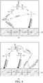
- FIG. 4 shows a process of producing a passivation layer 120 with HMDSO.
- FIG. 4(a) shows a process of depositing HMDSO in plasma phase.
- FIG. 4 (b) shows a process in which oxygen in plasma phase reacts with HMDSP in plasma phase.
- inert gas such as argon (Ar) may be introduced to facilitate the reaction.
- the hydrogen atoms contained in the Si-CH 3 bonding are diffused over time.
- the hydrogen atoms cause the above-mentioned issue, i.e., undesired TFT characteristics shift.
- the passivation layer 120 produced according to the process shown in FIG. 4(b) there exist an extremely small number of Si-CH 3 bondings, and thus the issue caused by diffused hydrogen atoms can be suppressed.
- the passivation layer 120 is especially advantageous for an OLED device employing oxide TFTs, since a pixel drive circuit including a TFT having an oxide semiconductor layer is more affected by hydrogen.
- the amount of the Si-CH 3 bondings is much smaller than the amount of the Si-O bondings, such as, 1 / 1000 or less.
- Fourier-Transform infrared spectroscopy may be used.
- the FT-IR is a kind of infrared spectroscopy that uses white light in infrared range whose phase has been modulated by an interferometer. Specifically, infrared ray is irradiated onto a sample, and an energy absorption corresponding to the vibration and rotation of a molecule under dipole moment change is measured. In a molecule, atoms are vibrating or rotating.
- the molecule absorbs light of a specific wavelength in the infrared range.
- the wavelength of the absorbed light is determined by the bonding between atoms in a molecule, almost irrespectively of the size of the molecule or structure of other portions. Accordingly, by analyzing it, information on the type of the bonding between atoms, a functional group of the molecule, etc. can be obtained.
- FIG. 5 is a graph showing some results of analyzing the passivation layers produced by the processes shown in FIG. 4 , respectively, using FT-IR.
- FIG. 5 (a) is a graph showing some results of analyzing the passivation layer produced by the process shown in FIG. 4 (a) .
- FIG. 5 (b) is a graph showing some results of analyzing the passivation layer produced by the process shown in FIG. 4(b) .
- a particular bonding reaction to a specific wavelength is shown as a peak. It can be seen that a peak appears at a wavelength corresponding to Si-CH 3 bonding in FIG. 5(a) , but not in FIG. 5(b) . That is, it can be concluded that there are minimal Si-CH 3 bondings resulting in the passivation layer produced by the process of the present embodiments as shown in FIG. 4(b) .
- an interval on the graph shown in FIG. 5 corresponding to the bonding is integrated, and the value may be expressed as the intensity of the bonding.
- a ratio of intensity between Si-CH 3 bonding and Si-O bonding is approximately 4/1,000.
- a ratio of intensity between Si-CH 3 bonding and Si-O bonding approximate to zero.
- Table 1 the reliability of samples with the characteristics shown in FIG. 5 was tested, and the results are shown in Table 1. As can be seen from Table 1, the sample with the characteristics shown in FIG. 5 (a) had strong bright spots viewable on a display screen, but the sample with the characteristics shown in FIG. 5(b) did not.
- reaction gases HMDSO and O 2 /N 2 O
- a processing temperature a processing temperature
- a processing pressure a processing pressure
- energy required to ionize reaction gas into plasma RF power or the like
- an organosilicon compound is used in the process of depositing a passivation layer, and the organosilicon compound reacts with oxygen (O 2 ) , ozone (O 3 ) or dinitrogen monoxide (N 2 O) in plasma phase, thereby fabricating a display device with improved reliability, over a passivation layer produced on the basis of SiH 4 or NH 3 .
- oxygen O 2
- O 3 ozone
- N 2 O dinitrogen monoxide
- a display device with reduced shift in the threshold voltage Vth of an oxide thin-film transistor (oxide TFT) can be obtained.
- the passivation layer may be produced by an oxidation reaction between the organosilicon and oxygen.
- the passivation layer may be produced as the organosilicon compound in plasma phase reacts with oxygen (O 2 ) , dinitrogen monoxide (N 2 O) or ozone (O 3 ) in plasma phase.
- the organosilicon compound may be HMDSO (hexamethyldisiloxane) or HMDSN (hexamethyldisilazane).
- the passivation layer may be deposited by CH 3 bonded to Si which is substituted with O.
- the passivation layer may include a Si-CH 3 bonding in less than 1/1000 of the amount of the Si-O bonding.
- the pixel drive circuit may include a thin-film transistor TFT having an oxide semiconductor layer.
- a shift in a threshold voltage of the thin-film transistor may be reduced compared with a case, in which the passivation layer was made based on silane (SiH 4 ) or ammonia (NH 3 ).
- the adhesive layer may include a first adhesive layer formed of a resin having moisture absorbents, and a second adhesive layer formed of a transparent resin.
- the first adhesive layer may be attached to a surface of an encapsulation plate facing the array substrate, and the second adhesive layer may be attached to the first adhesive layer, to the passivation layer and to a part of the array substrate around the passivation layer.
- the encapsulation plate may be made of glass, polymer or metal.
- the encapsulation plate may be configured to block permeation of moisture.
- the passivation layer may be configured to suppress shifts of a threshold voltage in a thin-film transistor due to diffused hydrogen atoms.
- the adhesive layer may be a face seal adhesive multi-layer structure in which multiple layers are stacked one on another.
- the adhesive layer may include a curable resin and a moisture adsorbent dispersed in the curable resin.
- a face seal encapsulation structure for an organic light-emitting display (OLED) device comprising: a passivation layer covering an organic light-emitting element, the passivation layer being an inorganic film based on an organosilicon compound; an encapsulation plate configured to block permeation of moisture; and an adhesive layer between the encapsulation plate and the passivation layer.
- OLED organic light-emitting display
- the passivation layer may be deposited by CH 3 bonded to Si, which is substituted with O in the organosilicon compound.
- the passivation layer may be configured to suppress shifts of a threshold voltage in a thin-film transistor due to diffused hydrogen atoms.
- the passivation layer may include Si-CH 3 bonding in less than 1/1000 of the amount of Si-O bonding.
- the passivation layer may be produced as a result of organosilicon compound in plasma phase reacting with oxygen (O 2 ) , di-nitrogen monoxide (N 2 O) or ozone (O 3 ) in plasma phase.
- the adhesive layer may be a face seal adhesive having multi-layer structure in which multiple layers are stacked one on another.
- the adhesive layer may include a curable resin and a moisture adsorbent dispersed in the curable resin.
- the encapsulation plate may be made of glass, polymer or metal.
Landscapes
- Physics & Mathematics (AREA)
- Optics & Photonics (AREA)
- Geometry (AREA)
- Engineering & Computer Science (AREA)
- Microelectronics & Electronic Packaging (AREA)
- Electroluminescent Light Sources (AREA)
Abstract
Description
- This application claims the priority of Korean Patent Application No.
10-2015-0167803 filed on November 27, 2015 - The present disclosure relates to an organic light-emitting display (OLED) device and an encapsulation structure.
- Display devices provide a variety of information graphically on a screen and are the core technology of information communications. Such display devices are becoming thinner, lighter and easier to carry, along with higher performance. With such trend, organic light-emitting display (OLED) devices are attracting attention, which control the amount of light emitted from an organic emission layer to display images.
- An OLED device is a self-luminous device using a thin emission layer between electrodes, and thus the overall device can be made thinner. Further, an OLED device is not only advantageous in terms of power consumption by low voltage driving, and also has excellent color implementation, response speed, viewing angle and contrast ratio (CR).
- In a typical OLED device, a pixel drive circuit and an organic light-emitting element are formed on a substrate, and light emitted from an organic light-emitting element may pass the substrate or a barrier layer, thereby displaying images. The organic light-emitting element can easily deteriorate by internal factors such as deterioration of the electrodes and the emission layer due to oxygen or moisture, deterioration by the reaction between the emission layer and interface, etc., as well as external factors such as moisture, oxygen, ultraviolet rays and processing limitations of the device. Among these, oxygen and moisture seriously affect the lifespan of the OLED device, and thus encapsulation of the OLED device is very important.
- As one of the encapsulation techniques, there is a known method of sealing the space above an organic light-emitting element with a passivation layer, or proving a face seal, or employing an encapsulation plate. The face seal contains moisture absorbent material to absorb moisture permeating into the organic light-emitting element. The face seal is applied on the inner surface of the encapsulation plate, and then the encapsulation plate is attached to a pixel array substrate. After the face seal sandwiched between the two substrate attached together (the encapsulation plate and the pixel array substrate) has been cured, pressure exerted against the substrates is removed, such that an OLED device having the face seal structure is fabricated. The encapsulation plate may be made of glass, plastic, metal or the like.
- In view of the above, an object of the present disclosure is to provide an OLED device and an improved encapsulation structure used therein. Another object of the present disclosure is to provide an organic element passivation layer with improved reliability.
- According to an aspect of the present disclosure, there is provided an OLED device including: a pixel drive circuit and organic light-emitting element on an array substrate; a passivation layer covering the pixel drive circuit and organic light-emitting element so as to block permeation of moisture; and an adhesive layer on the passivation layer. The passivation layer is an inorganic thin film based on an organosilicon compound.
- According to an exemplary embodiment of the present disclosure, a change in characteristics of a TFT due to hydrogen permeation can be reduced.
- According to another exemplary embodiment of the present disclosure, bright spots are reduced, such that the reliability of an OLED device can be improved.
- The above and other aspects, features and other advantages of the present disclosure will be more clearly understood from the following detailed description taken in conjunction with the accompanying drawings, in which:
-
FIG. 1 is a plan view of an OLED device according to an exemplary embodiment of the present disclosure; -
FIG. 2 is a cross-sectional view of a part of an active area of an OLED device according to an exemplary embodiment of the present disclosure; -
FIG. 3 is a view showing an encapsulation structure of an OLED device according to an exemplary embodiment of the present disclosure; -
FIG. 4 is a view showing a process of producing a passivation layer of an OLED device according to an exemplary embodiment of the present disclosure; and -
FIG. 5 is a graph showing characteristics of an OLED device according to an exemplary embodiment of the present disclosure. - In describing some components of exemplary embodiments of the present disclosure, terms such as first, second, A, B, (a), (b), etc., may be used. These terms are used only to differentiate a component from another component. Therefore, the nature, sequence, order, number, etc., of the components are not limited by these terms. As used herein, phrases "an element A connected to an element B" or "an element A coupled with an element B" refer to that the element A may be directly connected to/coupled with the element B, that that another element C may be interposed between the element A and the element B, and/or that the element A may be indirectly connected to/coupled with the element B via another element C. As used herein, a phrase "an element A on an element B" refers to that the element A may be disposed directly on the element B and/or the element A may be disposed indirectly on the element B via another element C. The drawings are not to scale and the relative dimensions of various elements in the drawings are depicted schematically and not necessarily to scale.
- As used herein, the term "OLED device" or "display device" collectively refers to an organic light-emitting diode panel and a display device employing such an organic light-emitting diode panel. Typically, OLED devices may be divided into white organic light-emitting display devices and RGB organic light-emitting display devices. In a white organic light-emitting device, sub-pixels in each of pixels emits white light, and a set of color filters is used in each of the sub-pixels to filter white light to produce red light, green light or blue light. In addition, a white organic light-emitting device may include sub-pixels with no color filter for forming sub-pixels for producing white light. On the other hand, in a RGB organic light-emitting device, an organic emission layer is configured to emit light of a particular color in each of sub-pixels. For example, a single pixel includes a red sub-pixel having an organic emission layer for emitting red light, a green sub-pixel having an organic emission layer for emitting green light, and a blue sub-pixel having an organic emission layer for emitting blue light.
- Features of various exemplary embodiments of the present disclosure may be combined partially or totally. As will be clearly appreciated by those skilled in the art, technically various interactions and operations are possible. Various exemplary embodiments can be practiced individually or in combination. Hereinafter, exemplary embodiments of the present disclosure will be described in detail with reference to the accompanying drawings.
-
FIG. 1 is a plan view of an organic light-emitting display (OLED) device according to an exemplary embodiment of the present disclosure. - Referring to
FIG. 1 , anOLED device 100 includes at least one active area A/A, in which an array of pixels is disposed. One or more inactive areas I/A may be disposed around the active area. That is, the inactive areas may be adjacent to one or more sides of the active area. InFIG. 1 , the inactive areas surround a rectangular active area. However, the shape of the active area and the shape/layout of the inactive areas adjacent to the active area are not limited to those shown inFIG. 1 . The active area and the inactive areas may have shapes appropriate for the design of an electronic device employing thedisplay device 100. For example, the active area may have a pentagon shape, a hexagon shape, a circle shape, an ellipse shape, etc. - Each of the pixels in the active area may be electrically connected to corresponding pixel drive circuits. Each of the pixel drive circuits may include at least one switching transistor and at least one driving transistor. Each of the pixel drive circuits may be electrically connected to gate lines and data lines so as to transfer signals with a gate driver, a data driver, etc., disposed in the inactive area.
- The gate driver and the data driver may be implemented with thin-film transistors (TFTs) in the inactive area. The drivers may be referred to GIP circuits (gate-in-panel) circuits. In addition, some components such as a data driver IC (integrated circuit) may be mounted on a separated PCB (printed circuit board) and may be coupled with a connection interface (a pad, a bump, a pin, etc.) disposed in the inactive area via a circuit film such as a FPCB (flexible printed circuit board), a COF (chip-on-film), a TCP (tape-carrier-package), etc. The printed circuits (COF, PCB, etc.) may be disposed behind the
display device 100 upon being folded over to a rear thereof. - The
OLED device 100 may include a variety of additional elements for generating various signals or voltages for driving the pixels in the active area. The additional elements for driving the pixels may include an inverter circuit, a multiplexer, an electro static discharge circuit, etc. TheOLED device 100 may include elements associated with features other than driving the pixels. For example, theOLED device 100 may include additional elements for providing a touch sense feature, a user authentication feature (e.g., fingerprint recognition), a multi-level pressure sense feature, a tactile feedback feature, etc. At least some of the above-mentioned additional elements may be disposed in the inactive areas and/or an external circuit connected to the connection interface. - The OLED device according to the exemplary embodiments of the present disclosure may include a thin-film transistor and an organic light-emitting element on an
array substrate 110, an encapsulation layer on the organic light-emitting element, a barrier film attaching the substrate to the encapsulation layer, and the like. Theterm array substrate 110 may also refer to the substrate itself as well as elements and functional layers formed thereon, e.g., a switching TFT, a driving TFT connected to the switching TFT, an organic light-emitting element connected to the driving TFT, a protective film, etc. - The
array substrate 110 supports a variety of elements of theOLED device 100 and is made of an insulative material. Thearray substrate 110 may be made of a transparent, insulative material such as glass, plastic, etc. - The organic light-emitting element is disposed on the
array substrate 110. The organic light-emitting element includes an anode, an organic emission layer formed on the anode, and a cathode formed on the organic emission layer. The organic emission layer may be made up of a single emission layer emitting light of a color or may be made up of a plurality of emission layers to emit white light. The organic light-emitting element may be formed in the center of thearray substrate 110 such that it is located in the active area. In the case that the organic emission layer of the organic light-emitting element emits white light, color filters may be further disposed. - The passivation layer may cover the organic light-emitting element. The passivation layer protects the organic light-emitting element from moisture or oxygen. A face seal may be used on the passivation layer. Examples of the face seal include a face seal adhesive film. The face seal adhesive film seals the organic light-emitting element disposed on the
array substrate 110 and attaches thearray substrate 110 to an upper substrate (encapsulation plate). -
FIG. 2 is a cross-sectional view of a part of the active area of the OLED device according to an exemplary embodiment of the present disclosure. -
FIG. 2 shows a thin-filmtransistor including elements array substrate 110, an organic light-emittingelement including elements - The
array substrate 110 may be a glass or plastic substrate. Such a plastic substrate may be made of polyimide-based material or polycarbonate-based material and thus may have flexibility. - The thin-film transistor may be formed by sequentially stacking a
semiconductor layer 102 on thearray substrate 110, agate insulation film 103, agate electrode 104, aninterlayer insulation film 105, and a source electrode and adrain electrode - The
semiconductor layer 102 may be made of a polysilicon (p-Si) and may be partially doped with impurities. In addition, thesemiconductor layer 102 may be made of amorphous silicon (a-Si) or may be made of a variety of organic semiconductor material such as pentacene. Further, thesemiconductor layer 102 may be made of oxide semiconductor material. - The
gate insulation film 103 may be formed of an insulative inorganic material such as a silicon oxide (SiOx) and a silicon nitride (SiNx) or may be made of an insulative organic material. Thegate electrode 104 may be made of a variety of conductive materials such as magnesium (Mg), aluminum (Al), nickel (Ni), chrome (Cr), molybdenum (Mo), tungsten (W), gold (Au) or an alloy thereof. - The
interlayer insulation film 105 may be formed of an insulative material such as a silicon oxide (SiOx) and a silicon nitride (SiNx) or may be made of an insulative organic material. By selectively removing theinterlayer insulation film 105 and thegate insulation film 103, contact holes may be formed via which a source region and a drain region are exposed. - The source electrode and the
drain electrode gate electrode 104 and consist of a single layer or a plurality of layers on theinterlayer insulation film 105 such that the contact holes are filled. - A
planarization layer 107 may be disposed on the thin-film transistor. Theplanarization layer 107 protects the thin-film transistor and provides a flat surface. Theplanarization layer 107 may have a variety of forms. For example, thepassivation layer 107 may be made of an organic insulation film such as BCB (benzocyclobutene) and acryl or may be made of an inorganic insulation film such as silicon nitride (SiNx) film and silicon oxide (SiOx) film. In addition, thepassivation layer 107 may be made up of a single layer, a double layer, or a multi-layer. - The organic light-emitting element may be formed by stacking a
first electrode 112, anorganic emission layer 114 and asecond electrode 116 in this order. That is, the organic light-emitting element may include thefirst electrode 112 formed on theplanarization layer 107, theorganic emission layer 114 disposed on thefirst electrode 112, and thesecond electrode 116 disposed on theorganic emission layer 114. - The
first electrode 112 is electrically connected to thedrain electrode 108 of the driving thin-film transistor via the contact hole. In the case if theOLED device 100 is of top-emission type, thefirst electrode 112 may be made of an opaque conductive material having high reflectivity. For example, thefirst electrode 112 may be made of silver (Ag), aluminum (Al), gold (Au), molybdenum (Mo), tungsten (W), chrome (Cr) or an alloy thereof. - A bank 109 (or other structure with similar functions) is formed in the rest of the area other than an emission area. Accordingly, the
bank 109 has a bank hole via which thefirst electrode 112 in the emission area is exposed. Thebank 109 may be made of an inorganic insulative material such as silicon nitride (SiNx) film and silicon oxide (SiOx) film or an organic insulative material such as BCB, acryl-based resin or imide-based resin. - The
organic emission layer 114 is disposed on thefirst electrode 112 exposed via the hole of thebank 109. Theorganic emission layer 114 may include an emission layer, an electron injection layer, an electron transport layer, a hole transport layer, a hole injection layer, etc. Such layers may be independent and discrete, or some functionality may be combined together as a single layer. - The
second electrode 116 is disposed on theorganic emission layer 114. In the case, if theOLED device 100 is of top-emission type, thesecond electrode 116 is made of a transparent, conductive material such as indium tin oxide (ITO) or indium zinc oxide (IZO), such that light generated in theorganic emission layer 114 exits upwardly through thesecond electrode 116. - The
passivation layer 120 is disposed on thesecond electrode 116. Thepassivation layer 120 may be configured as an inorganic film made of glass, metal, aluminum oxide (AlOx) or silicon (Si)-based material or may be formed by stacking organic films and inorganic films alternately. Thepassivation layer 120 blocks oxygen and moisture from permeating to thereby suppress oxidation of luminous material and the material of the electrodes. If an organic light-emitting element is exposed to moisture or oxygen, the emission area may shrink, i.e., pixel shrinkage may take place or dark spots may appear in the emission area. - An
adhesive layer 140 may be disposed on thepassivation layer 120. Theadhesive layer 140 seals the organic light-emitting element and attaches thearray substrate 110 to anencapsulation plate 190. - The
encapsulation plate 190 faces thearray substrate 110. The lower surface of theencapsulation plate 190 comes in contact with theadhesive layer 140. Theencapsulation plate 190 may be made of a material such as glass, polymer, metal, etc. The material of theencapsulation plate 190 may be determined based on the direction in which theOLED device 100 emits light, i.e. the direction of top emission, bottom emission or dual-sided emission. - The
adhesive layer 140 is disposed between the pixel drive circuit and organic light-emitting element TFT/OLED and theencapsulation plate 190 thereon. Typically, theadhesive layer 140 is attached on theencapsulation plate 190, and then theencapsulation plate 190 is attached to thearray substrate 110 with theadhesive layer 140 facing the pixel drive circuit and organic light-emitting element TFT/OLED. - A lower
adhesive layer 160 and alower encapsulation layer 170 are formed under thearray substrate 110 in this order. Thelower encapsulation layer 170 may be made of at least one organic material selected from the group consisting of: polyethylene naphthalate (PEN), polyethylene terephthalate (PET), polyethylene ether phthalate, polycarbonate, polyarylate, polyether imide, polyether sulfonate, polyimide and polyacrylate. Thelower encapsulation layer 170 may suppress moisture or oxygen from permeating into the substrate. - The lower
adhesive layer 160 is made of thermosetting adhesive or a naturally-curable adhesive and attaches thearray substrate 110 to thelower encapsulation layer 170. For example, the loweradhesive layer 160 may be made of an optically clear adhesive (OCA). -
FIG. 3 is a cross-sectional view showing an encapsulation structure of an OLED device according to an exemplary embodiment of the present disclosure. - The
OLED device 100 may include anarray substrate 110, a pixel drive circuit and organic light-emitting element TFT/OLED, apassivation layer 120, anadhesive layer 140, and anencapsulation plate 190. - The
array substrate 110 is made of an insulative material and supports a variety of elements of theOLED device 100. - The pixel drive circuit and organic light-emitting element TFT/OLED is disposed on the
array substrate 110. The organic light-emitting element includes an anode, an organic emission layer formed on the anode, and a cathode formed on the organic emission layer. The organic emission layer may be made up of a single emission layer emitting light of a color or may be made up of a plurality of emission layers to emit white light. The organic light-emitting element may be formed on thearray substrate 110 such that it is located in the active area. A pixel drive circuit for driving the organic light-emitting element, i.e., a variety of elements such as thin-film transistors, capacitors, etc., and lines may be disposed in association with the organic light-emitting element. The structure and function of the pixel drive circuit and the organic light-emitting element are substantially identical to those described above with reference toFIG. 2 . - The
OLED device 100 includes an encapsulation structure for covering the organic light-emitting element to block permeation of moisture or oxygen. The encapsulation structure may be a face seal structure including a passivation layer, an adhesive layer and an encapsulation plate. - The
passivation layer 120 is a functional layer for protecting the pixel drive circuit and organic light-emitting element TFT/OLED, and covers the pixel drive circuit and organic light-emitting element TFT/OLED to block the permeation of moisture or oxygen. Thepassivation layer 120 may be an inorganic film or may be formed by stacking organic films and inorganic films alternately. For example, thepassivation layer 120 may be an inorganic thin film based on an organosilicon compound. Thepassivation layer 120 is advantageous over a passivation layer made based on silane (SiH4) or ammonia (NH3), in that a shift in the threshold voltage of the oxide thin-film transistor (oxide TFT) is reduced. More detailed description thereon will be made with reference toFIG. 4 . - The
adhesive layer 140 seals the organic light-emitting element and attaches thearray substrate 110 to theencapsulation plate 190. Theadhesive layer 140 may be made of a mixture of a curable resin and a functional additive. For example, theadhesive layer 140 may be made of a curable resin and a getter and/or filler dispersed in the curable resin. The curable resin may be made of, but is not limited to, an epoxy-based polymer, an olefin-based polymer, etc. - The
adhesive layer 140 may be a face seal adhesive having multi-layer structure in which multiple layers are stacked one on another vertically. For example, theadhesive layer 140 may be a face seal adhesive including a first layer (a first adhesive layer) and a second layer (a second adhesive layer). - The
first layer 141 may also be referred to as a barrier layer (B-layer) and may be attached to a surface of theencapsulation plate 190 facing the array substrate110. Thefirst layer 141 may be made of curable resin 141b containingmoisture adsorbent 141a. Themoisture adsorbent 141a of thefirst layer 141 act to adsorb or remove moisture or oxygen by physical or chemical reaction, etc. For example, themoisture adsorbent 141a may be a reactive adsorbent such as metal powder including alumina, a metal oxide, a metal salt, phosphorous pentoxide (P2O5) or a mixture thereof. For another example, the moisture absorbent 141-1a may be a physical adsorbent such as silica, zeolite, titania, zirconia, montmorillonite, etc. - The metal oxide may be lithium oxide (Li2O), sodium oxide (Na2O), barium oxide (BaO), calcium oxide (CaO) or magnesium oxide (MgO). The metal salt may be a sulfate such as lithium sulfate (Li2SO4), sodium sulfate (Na2SO4), calcium sulfate (CasO4), magnesium sulfate (MgsO4), cobalt sulfate (CoSO4), gallium sulfate (Ga2(SO4)3), titanium sulfate (Ti(SO4)2) or nickel sulfate (NiSO4). In addition, the metal salt may be a metal halide such as calcium chloride (CaCl2), magnesium chloride (MgCl2), strontium chloride (SrCl2), chloride, yttrium (YCl3), copper chloride (CuCl2), cesium fluoride (CsF), fluoride tantalum (TaF5), fluoride, niobium (NbF5), lithium bromide (LiBr), calcium bromide (CaBr2), cesium bromide (CeBr3), selenium bromide (SeBr4), vanadium bromide (VBr3), magnesium bromide (MgBr2), barium iodide (BaI2) or magnesium iodide (MgI2), or a metal chlorate such as barium perchlorate (Ba (ClO4)2), magnesium perchlorate (Mg(ClO4)2). It is to be noted that the moisture adsorbent is not limited to those listed above.
- The
second layer 142 may also be referred to as a transparent layer (T-layer). Thesecond layer 142 is made basically of a transparent curable resin. The secondadhesive layer 142 may be a thermosetting resin or a photo-curable resin. The curable resin of thesecond layer 142 may be the same as or different from the curable resin 141b of thefirst layer 141. For example, the curable resin 141b may be a thermosetting resin that includes at least one heat-curable functional group such as glycidyl group, isocyanate group, hydroxyl group, carboxyl group, amide group or the like. - A face of the
second layer 142 comes in contact with thearray substrate 110 and the organic light-emitting element (or an insulation film thereon) and may mitigate a pressure exerted when thearray substrate 110 is attached to theencapsulation plate 190. The other face of thesecond layer 142 comes in contact with a face of thefirst layer 141. - The
encapsulation plate 190 faces thearray substrate 110. The lower surface of theencapsulation plate 190 comes in contact with theadhesive layer 140. Theencapsulation plate 190 may be made of a material such as glass, polymer, metal, etc. The material of theencapsulation plate 190 may be determined based on the direction in which theOLED device 100 emits light. - Referring to
FIG. 3 , theadhesive layer 140 is disposed between the pixel drive circuit and organic light-emitting element TFT/OLED and theencapsulation plate 190 thereon. Typically, theadhesive layer 140 is attached on theencapsulation plate 190, and then theencapsulation plate 190 is attached to thearray substrate 110 with theadhesive layer 140 facing the pixel drive circuit and organic light-emitting element TFT/OLED. -
FIG. 4 shows a process of forming a passivation layer according to an exemplary embodiment of the present disclosure. - The
passivation layer 120 is a functional layer for protecting the pixel drive circuit and organic light-emitting element TFT/OLED, and covers the pixel drive circuit and organic light-emitting element TFT/OLED to block the permeation of moisture or oxygen. For example, thepassivation layer 120 may be an inorganic thin film based on an organosilicon compound. Thepassivation layer 120 is advantageous over a passivation layer made based on silane (SiH4) or ammonia (NH3), in that a shift in the threshold voltage of the oxide thin-film transistor (oxide TFT) is reduced. - The
passivation layer 120 may be formed by depositing a silicon nitride (SiNx)-based or silicon oxide (SiOx)-based compound on the pixel drive circuit and organic light-emitting element TFT/OLED using a plasma enhanced chemical vapor deposition (PECVD) technique, or by depositing an aluminum oxide (AlOx)-based compound using sputtering. Typically, silane (SiH4) gas and ammonia (NH3) gas are used in the PECVD process to form the SiNx-based or SiOx-based film. - For an OLED device, the PECVD process is carried out at a temperature lower than 100°C in order to avoid deterioration of the OLED device. During the PECVD process, chemical reactions may proceed incompletely, such that hydrogen atoms (H) contained in the SiH4 and NH3 based gas may remain on the
passivation layer 120. The hydrogen atoms remaining on thepassivation layer 120 is diffused even to the pixel drive circuit over time. The diffused hydrogen atoms reduce the oxide semiconductor layer (a channel layer) of the thin-film transistor included in the pixel drive circuit, thereby deteriorating the performance of the thin-film transistor. For example, the diffused hydrogen atoms may shift the threshold voltage Vth of the oxide thin-film transistor (oxide TFT), thereby causing screen spots or uneven brightness. - In order to solve such problems recognized by the present inventors, according to an exemplary embodiment of the present disclosure, there is provided a
passivation layer 120 suppressing the diffused hydrogen issue and a method for producing it. According to an exemplary embodiment of the present disclosure, there is provided a structure of apassivation layer 120 that reduces Si-CH3 bondings by using a reaction by which an organosilicon compound is polymerized by oxygen (O2) , ozone (O3) or di-nitrogen monoxide (N2O) plasma. Typically, hydrogen atoms contained in the Si-CH3 bondings have weak bonding force since they react at a low temperature, and thus they are diffused over time, such that the above-mentioned issue takes place. Accordingly, by reducing the number (amount) of Si-CH3 bondings due to the polymerization method described herein, the issues or problems associated with the diffused hydrogen atoms can be effectively suppressed. - The organosilicon compound may be, for example, HMDSN (hexamethyldisilazane: C6H19NSi2) or HMDSO (hexamethyldisiloxane: C6H18OSi2).
FIG. 4 shows a process of producing apassivation layer 120 with HMDSO.FIG. 4(a) shows a process of depositing HMDSO in plasma phase.FIG. 4 (b) shows a process in which oxygen in plasma phase reacts with HMDSP in plasma phase. In the reaction shown inFIG. 4 , inert gas such as argon (Ar) may be introduced to facilitate the reaction. - In the process shown in
FIG. 4(a) , after the Si-O bonding of the HMDSO dissociate from each other, a part thereof is deposited as SiO(CH3)3, forming thepassivation layer 120. In the process shown inFIG. 4B , on the other hand, after the Si-O bonding of the HMDSO dissociate from each other, a methyl group (CH3) is substituted with an oxygen atom (O), forming thepassivation layer 120. As a result, the contents of carbon atoms (C) and hydrogen atoms (H) in thepassivation layer 120 become extremely small. That is, in the process shown inFIG. 4(b) , thepassivation layer 120 is produced by the oxidation reaction between the organosilicon compound and oxygen (or dinitrogen monoxide, ozone). - In the
passivation layer 120 produced according to the process shown inFIG. 4(a) , the hydrogen atoms contained in the Si-CH3 bonding are diffused over time. The hydrogen atoms cause the above-mentioned issue, i.e., undesired TFT characteristics shift. In contrast, in thepassivation layer 120 produced according to the process shown inFIG. 4(b) , there exist an extremely small number of Si-CH3 bondings, and thus the issue caused by diffused hydrogen atoms can be suppressed. - That is, the less Si-CH3 bondings are in the
passivation layer 120, the better performance the display device exhibits. Thepassivation layer 120 according to the exemplary embodiment of the present disclosure is especially advantageous for an OLED device employing oxide TFTs, since a pixel drive circuit including a TFT having an oxide semiconductor layer is more affected by hydrogen. - For example, the amount of the Si-CH3 bondings is much smaller than the amount of the Si-O bondings, such as, 1 / 1000 or less. In order to quantitatively measure the amounts of a variety of bondings in a compound, Fourier-Transform infrared spectroscopy (FT-IR) may be used. The FT-IR is a kind of infrared spectroscopy that uses white light in infrared range whose phase has been modulated by an interferometer. Specifically, infrared ray is irradiated onto a sample, and an energy absorption corresponding to the vibration and rotation of a molecule under dipole moment change is measured. In a molecule, atoms are vibrating or rotating. By such movement, the molecule absorbs light of a specific wavelength in the infrared range. The wavelength of the absorbed light is determined by the bonding between atoms in a molecule, almost irrespectively of the size of the molecule or structure of other portions. Accordingly, by analyzing it, information on the type of the bonding between atoms, a functional group of the molecule, etc. can be obtained.
-
FIG. 5 is a graph showing some results of analyzing the passivation layers produced by the processes shown inFIG. 4 , respectively, using FT-IR.FIG. 5 (a) is a graph showing some results of analyzing the passivation layer produced by the process shown inFIG. 4 (a) .FIG. 5 (b) is a graph showing some results of analyzing the passivation layer produced by the process shown inFIG. 4(b) . On the graphs, a particular bonding reaction to a specific wavelength is shown as a peak. It can be seen that a peak appears at a wavelength corresponding to Si-CH3 bonding inFIG. 5(a) , but not inFIG. 5(b) . That is, it can be concluded that there are minimal Si-CH3 bondings resulting in the passivation layer produced by the process of the present embodiments as shown inFIG. 4(b) . - In order to quantitatively measure a particular bonding by FT-IR analysis, an interval on the graph shown in
FIG. 5 corresponding to the bonding is integrated, and the value may be expressed as the intensity of the bonding. InFIG. 5(a) , a ratio of intensity between Si-CH3 bonding and Si-O bonding is approximately 4/1,000. InFIG. 5(b) , a ratio of intensity between Si-CH3 bonding and Si-O bonding approximate to zero. In addition, the reliability of samples with the characteristics shown inFIG. 5 was tested, and the results are shown in Table 1. As can be seen from Table 1, the sample with the characteristics shown inFIG. 5 (a) had strong bright spots viewable on a display screen, but the sample with the characteristics shown inFIG. 5(b) did not.[Table 1] (a) (b) Strong Bright Spot Occurrence Occurred@300hrs Not occurred@850hrs Number of Panels (Occurrence/Total Number) 4 / 4 0 / 11 FT-IR (Si-CH3/SiOx * 10,000) 41 0 - After repeating such tests, the present inventors have found out that no bright spots appeared when the ratio between Si-CH3 bonding and Si-O bonding is approximately 1 / 1,000 or less.
- In order to reduce such undesired Si-CH3 bondings, the present inventors recognized that a ratio between reaction gases (HMDSO and O2/N2O), a processing temperature, a processing pressure, energy required to ionize reaction gas into plasma (RF power or the like), etc., have to be considered.
- According to exemplary embodiments of the present disclosure, an organosilicon compound is used in the process of depositing a passivation layer, and the organosilicon compound reacts with oxygen (O2) , ozone (O3) or dinitrogen monoxide (N2O) in plasma phase, thereby fabricating a display device with improved reliability, over a passivation layer produced on the basis of SiH4 or NH3. As a result, a display device with reduced shift in the threshold voltage Vth of an oxide thin-film transistor (oxide TFT) can be obtained.
- Exemplary embodiments of the present disclosure can also be described as follows:
- According to an aspect of the present disclosure, there is provided an OLED device. The OLED device includes: an array substrate; a pixel drive circuit and an organic light-emitting element on the array substrate; a passivation layer covering the pixel drive circuit and organic light-emitting element so as to block permeation of moisture; and an adhesive layer on the passivation layer. The passivation layer is an inorganic thin film based on an organosilicon compound.
- The passivation layer may be produced by an oxidation reaction between the organosilicon and oxygen.
- The passivation layer may be produced as the organosilicon compound in plasma phase reacts with oxygen (O2) , dinitrogen monoxide (N2O) or ozone (O3) in plasma phase.
- The organosilicon compound may be HMDSO (hexamethyldisiloxane) or HMDSN (hexamethyldisilazane).
- The passivation layer may be deposited by CH3 bonded to Si which is substituted with O.
- The passivation layer may include a Si-CH3 bonding in less than 1/1000 of the amount of the Si-O bonding.
- The pixel drive circuit may include a thin-film transistor TFT having an oxide semiconductor layer.
- A shift in a threshold voltage of the thin-film transistor may be reduced compared with a case, in which the passivation layer was made based on silane (SiH4) or ammonia (NH3).
- The adhesive layer may include a first adhesive layer formed of a resin having moisture absorbents, and a second adhesive layer formed of a transparent resin.
- The first adhesive layer may be attached to a surface of an encapsulation plate facing the array substrate, and the second adhesive layer may be attached to the first adhesive layer, to the passivation layer and to a part of the array substrate around the passivation layer.
- The encapsulation plate may be made of glass, polymer or metal.
- The encapsulation plate may be configured to block permeation of moisture.
- The passivation layer may be configured to suppress shifts of a threshold voltage in a thin-film transistor due to diffused hydrogen atoms.
- The adhesive layer may be a face seal adhesive multi-layer structure in which multiple layers are stacked one on another.
- The adhesive layer may include a curable resin and a moisture adsorbent dispersed in the curable resin.
- According to another aspect of the present disclosure, there is provided a face seal encapsulation structure for an organic light-emitting display (OLED) device, comprising: a passivation layer covering an organic light-emitting element, the passivation layer being an inorganic film based on an organosilicon compound; an encapsulation plate configured to block permeation of moisture; and an adhesive layer between the encapsulation plate and the passivation layer.
- The passivation layer may be deposited by CH3 bonded to Si, which is substituted with O in the organosilicon compound.
- The passivation layer may be configured to suppress shifts of a threshold voltage in a thin-film transistor due to diffused hydrogen atoms.
- The passivation layer may include Si-CH3 bonding in less than 1/1000 of the amount of Si-O bonding.
- The passivation layer may be produced as a result of organosilicon compound in plasma phase reacting with oxygen (O2) , di-nitrogen monoxide (N2O) or ozone (O3) in plasma phase.
- The adhesive layer may be a face seal adhesive having multi-layer structure in which multiple layers are stacked one on another.
- The adhesive layer may include a curable resin and a moisture adsorbent dispersed in the curable resin.
- The encapsulation plate may be made of glass, polymer or metal.
Claims (15)
- An organic light-emitting display device (100), comprising:an array substrate (110)a pixel drive circuit and an organic light-emitting element (TFT/OLED) on the array substrate (110);a passivation layer (120), consisting of an inorganic thin film based on an organosilicon compound, covering the pixel drive circuit and the organic light-emitting element (TFT/OLED) so as to block permeation of moisture; andan adhesive layer (140) on the passivation layer (120).
- The organic light-emitting display device (100) of claim 1, wherein the passivation layer (120) is produced by an oxidation reaction between organosilicon and oxygen.
- The organic light-emitting display device (100) of claim 2, wherein the passivation layer (120) is produced as a result of the organosilicon compound in plasma phase reacting with oxygen, di-nitrogen monoxide or ozone in plasma phase.
- The organic light-emitting display device (100) of claim 2 or 3, wherein the organosilicon compound is hexamethyldisiloxane or hexamethyldisilazane.
- The organic light-emitting display device (100) of claim 3 or 4, wherein the passivation layer (120) is deposited by CH3 bonded to Si, which is substituted with O, in the organosilicon compound.
- The organic light-emitting display device (100) of claim 5, wherein the passivation layer (120) includes Si-CH3 bonding in less than 1/1000 of the amount of Si-O bonding.
- The organic light-emitting display device (100) of any one of claims 1 to 6, wherein the pixel drive circuit comprises a thin-film transistor having an oxide semiconductor layer.
- The organic light-emitting display device (100) of claim 7, wherein a shift in a threshold voltage of the thin-film transistor is reduced compared with a case, in which the passivation layer (120) was made based on silane or ammonia.
- The organic light-emitting display device (100) of any one of claims 1 to 8, wherein the adhesive layer (140) comprises a first adhesive layer (141) formed of a resin having moisture absorbent material, and a second adhesive layer (142) formed of a transparent resin.
- The organic light-emitting display device (100) of claim 9, further comprising an encapsulation plate (190), wherein the first adhesive layer (141) is attached to a surface of the encapsulation plate (190) facing the array substrate (110), and the second adhesive layer (142) is attached to the first adhesive layer (141), to the passivation layer (120) and to a part of the array substrate (110) around the passivation layer (120).
- The organic light-emitting display device (100) of claim 10, wherein the encapsulation plate (190) is made of glass, polymer or metal.
- The organic light-emitting display device (100) of claim 10 or 11, wherein the encapsulation plate (190) is configured to block permeation of moisture.
- The organic light-emitting display device (100) of any one of claims 1 to 6, wherein the passivation layer (120) is configured to suppress shifts of a threshold voltage in a thin-film transistor due to diffused hydrogen atoms.
- The organic light-emitting display (device (100) of any one of claims 1 to 8, wherein the adhesive layer (120) is a face seal adhesive having multi-layer structure in which multiple layers are stacked one on another.
- The organic light-emitting display (device (100) of claim 14, wherein the adhesive layer (120) comprises a curable resin and a moisture adsorbent dispersed in the curable resin.
Priority Applications (1)
| Application Number | Priority Date | Filing Date | Title |
|---|---|---|---|
| EP22207999.8A EP4156883A1 (en) | 2015-11-27 | 2016-11-11 | Organic light-emitting display device |
Applications Claiming Priority (1)
| Application Number | Priority Date | Filing Date | Title |
|---|---|---|---|
| KR1020150167803A KR102461970B1 (en) | 2015-11-27 | 2015-11-27 | Organic light emitting display device |
Related Child Applications (2)
| Application Number | Title | Priority Date | Filing Date |
|---|---|---|---|
| EP22207999.8A Division-Into EP4156883A1 (en) | 2015-11-27 | 2016-11-11 | Organic light-emitting display device |
| EP22207999.8A Division EP4156883A1 (en) | 2015-11-27 | 2016-11-11 | Organic light-emitting display device |
Publications (2)
| Publication Number | Publication Date |
|---|---|
| EP3174120A1 true EP3174120A1 (en) | 2017-05-31 |
| EP3174120B1 EP3174120B1 (en) | 2023-01-04 |
Family
ID=57286370
Family Applications (2)
| Application Number | Title | Priority Date | Filing Date |
|---|---|---|---|
| EP22207999.8A Pending EP4156883A1 (en) | 2015-11-27 | 2016-11-11 | Organic light-emitting display device |
| EP16198400.0A Active EP3174120B1 (en) | 2015-11-27 | 2016-11-11 | Organic light-emitting display device |
Family Applications Before (1)
| Application Number | Title | Priority Date | Filing Date |
|---|---|---|---|
| EP22207999.8A Pending EP4156883A1 (en) | 2015-11-27 | 2016-11-11 | Organic light-emitting display device |
Country Status (4)
| Country | Link |
|---|---|
| US (1) | US10600994B2 (en) |
| EP (2) | EP4156883A1 (en) |
| KR (2) | KR102461970B1 (en) |
| CN (1) | CN106816548B (en) |
Cited By (2)
| Publication number | Priority date | Publication date | Assignee | Title |
|---|---|---|---|---|
| US10910584B2 (en) | 2017-10-18 | 2021-02-02 | Samsung Display Co., Ltd. | Light emitting device having insulation layer of varying thickness and manufacturing method thereof |
| EP3869560A1 (en) * | 2020-02-24 | 2021-08-25 | Samsung Display Co., Ltd. | Thin-film transistor substrate, display apparatus including the same, and method of manufacturing display apparatus |
Families Citing this family (24)
| Publication number | Priority date | Publication date | Assignee | Title |
|---|---|---|---|---|
| KR102511413B1 (en) | 2015-12-15 | 2023-03-16 | 엘지디스플레이 주식회사 | Organic light emitting display device |
| KR102316563B1 (en) | 2017-05-22 | 2021-10-25 | 엘지디스플레이 주식회사 | Organic Light-Emitting Display device having an upper substrate formed by a metal and Method of fabricating the same |
| WO2018226077A1 (en) * | 2017-06-09 | 2018-12-13 | 주식회사 엘지화학 | Encapsulation film |
| JP7113376B2 (en) * | 2017-06-14 | 2022-08-05 | パナソニックIpマネジメント株式会社 | DISPLAY DEVICE AND METHOD FOR MANUFACTURING DISPLAY DEVICE |
| CN109096932B (en) * | 2017-06-29 | 2020-03-24 | 新和因特泰科株式会社 | Adhesive film and organic electronic device comprising same |
| KR102398554B1 (en) * | 2017-08-31 | 2022-05-17 | 엘지디스플레이 주식회사 | Organic Light-Emitting Display device having an encapsulating layer |
| CN107785503B (en) | 2017-10-24 | 2019-03-08 | 京东方科技集团股份有限公司 | Metal packaging structure and preparation method, packaging method of display panel, display device |
| KR102413223B1 (en) * | 2017-12-19 | 2022-06-24 | 쑤저우 레킨 세미컨덕터 컴퍼니 리미티드 | Light emitting device package |
| JP6983084B2 (en) * | 2018-02-07 | 2021-12-17 | 株式会社ジャパンディスプレイ | Organic EL display device |
| US10879489B2 (en) * | 2018-05-21 | 2020-12-29 | Korea Advanced Institute Of Science And Technology | Organic device having protective film and method of manufacturing the same |
| KR102656235B1 (en) * | 2018-08-17 | 2024-04-09 | 엘지디스플레이 주식회사 | Display device having an encapsulating substrate of high thermal conductivity |
| JP7195685B2 (en) * | 2018-09-03 | 2022-12-26 | エルジー・ケム・リミテッド | sealing film |
| KR102745474B1 (en) * | 2018-11-16 | 2024-12-20 | 엘지디스플레이 주식회사 | Organic light emitting display device display device |
| CN109817817A (en) * | 2019-01-30 | 2019-05-28 | 武汉华星光电半导体显示技术有限公司 | A kind of flexible OLED device and preparation method thereof |
| CN110707230A (en) * | 2019-09-04 | 2020-01-17 | 深圳市华星光电技术有限公司 | OLED packaging structure and display panel |
| JP2021067763A (en) * | 2019-10-21 | 2021-04-30 | 株式会社ジャパンディスプレイ | Display device and manufacturing method for display device |
| CN111029397A (en) * | 2019-12-27 | 2020-04-17 | 安徽熙泰智能科技有限公司 | Silicon-based OLED micro-display device and preparation method thereof |
| KR102689907B1 (en) * | 2019-12-30 | 2024-07-29 | 엘지디스플레이 주식회사 | Display apparatus |
| CN111312920A (en) * | 2020-02-17 | 2020-06-19 | 合肥鑫晟光电科技有限公司 | Display device and manufacturing method thereof |
| CN111540841A (en) * | 2020-04-30 | 2020-08-14 | 合肥维信诺科技有限公司 | Display panel, display mother board and manufacturing method of display panel |
| KR20230040307A (en) * | 2020-07-15 | 2023-03-22 | 가디언 글라스, 엘엘씨 | Dynamic Shades with Reactive Gas Compatible Desiccants and/or Related Methods |
| KR102838521B1 (en) * | 2020-12-31 | 2025-07-24 | 엘지디스플레이 주식회사 | Display apparatus |
| CN114203783A (en) * | 2021-12-09 | 2022-03-18 | 深圳市华星光电半导体显示技术有限公司 | Flexible display panel and manufacturing method thereof |
| US20230209915A1 (en) * | 2021-12-23 | 2023-06-29 | Lg Display Co., Ltd. | Display device |
Citations (2)
| Publication number | Priority date | Publication date | Assignee | Title |
|---|---|---|---|---|
| US20150069376A1 (en) * | 2011-06-10 | 2015-03-12 | Samsung Display Co., Ltd. | Organic light emitting diode display |
| EP2876701A1 (en) * | 2013-11-25 | 2015-05-27 | LG Display Co., Ltd. | Method for manufacturing organic light emitting diode display device |
Family Cites Families (12)
| Publication number | Priority date | Publication date | Assignee | Title |
|---|---|---|---|---|
| KR100462469B1 (en) * | 2002-04-17 | 2004-12-17 | 한국전자통신연구원 | Encapsulation thin films having bonding-type organic-inorganic complex film and organic electroluminescent devices including the same |
| JP2010044118A (en) * | 2008-08-08 | 2010-02-25 | Sony Corp | Display, and its manufacturing method |
| KR101846434B1 (en) * | 2011-06-10 | 2018-04-09 | 삼성디스플레이 주식회사 | Organic light emitting diode display |
| US8889567B2 (en) * | 2011-09-16 | 2014-11-18 | Taiwan Semiconductor Manufacturing Company, Ltd. | Apparatus and methods for low K dielectric layers |
| JPWO2013183289A1 (en) * | 2012-06-08 | 2016-01-28 | パナソニック株式会社 | THIN FILM TRANSISTOR, DISPLAY PANEL AND METHOD FOR PRODUCING THIN FILM TRANSISTOR |
| CN104640958B (en) * | 2012-09-18 | 2017-04-05 | 默克专利有限公司 | For the material of electronic device |
| KR102102103B1 (en) * | 2012-10-09 | 2020-04-20 | 메르크 파텐트 게엠베하 | Metal complexes |
| JP2014170686A (en) * | 2013-03-04 | 2014-09-18 | Toshiba Corp | Method for manufacturing display element, display element, and display device |
| TWI692108B (en) * | 2013-04-10 | 2020-04-21 | 日商半導體能源研究所股份有限公司 | Semiconductor device and manufacturing method thereof |
| US9268378B2 (en) * | 2013-06-28 | 2016-02-23 | Intel Corporation | Techniques and system for managing platform temperature |
| KR102109743B1 (en) * | 2013-12-09 | 2020-05-12 | 엘지디스플레이 주식회사 | Organic Light Emitting Display Apparatus and Method for Manufacturing The Same |
| KR102269133B1 (en) * | 2014-04-30 | 2021-06-25 | 삼성디스플레이 주식회사 | Flexible display apparatus and method for manufacturing the same |
-
2015
- 2015-11-27 KR KR1020150167803A patent/KR102461970B1/en active Active
-
2016
- 2016-11-11 EP EP22207999.8A patent/EP4156883A1/en active Pending
- 2016-11-11 EP EP16198400.0A patent/EP3174120B1/en active Active
- 2016-11-21 CN CN201611020621.1A patent/CN106816548B/en active Active
- 2016-11-25 US US15/361,341 patent/US10600994B2/en active Active
-
2022
- 2022-10-21 KR KR1020220136319A patent/KR102668191B1/en active Active
Patent Citations (2)
| Publication number | Priority date | Publication date | Assignee | Title |
|---|---|---|---|---|
| US20150069376A1 (en) * | 2011-06-10 | 2015-03-12 | Samsung Display Co., Ltd. | Organic light emitting diode display |
| EP2876701A1 (en) * | 2013-11-25 | 2015-05-27 | LG Display Co., Ltd. | Method for manufacturing organic light emitting diode display device |
Cited By (4)
| Publication number | Priority date | Publication date | Assignee | Title |
|---|---|---|---|---|
| US10910584B2 (en) | 2017-10-18 | 2021-02-02 | Samsung Display Co., Ltd. | Light emitting device having insulation layer of varying thickness and manufacturing method thereof |
| EP3869560A1 (en) * | 2020-02-24 | 2021-08-25 | Samsung Display Co., Ltd. | Thin-film transistor substrate, display apparatus including the same, and method of manufacturing display apparatus |
| US11864421B2 (en) | 2020-02-24 | 2024-01-02 | Samsung Display Co., Ltd. | Thin-film transistor, display apparatus including the same, and method of manufacturing display apparatus |
| US12317683B2 (en) | 2020-02-24 | 2025-05-27 | Samsung Display Co., Ltd. | Thin-film transistor, display apparatus including the same, and method of manufacturing display apparatus |
Also Published As
| Publication number | Publication date |
|---|---|
| EP3174120B1 (en) | 2023-01-04 |
| US10600994B2 (en) | 2020-03-24 |
| KR20220147564A (en) | 2022-11-03 |
| US20170155086A1 (en) | 2017-06-01 |
| EP4156883A1 (en) | 2023-03-29 |
| KR102668191B1 (en) | 2024-05-21 |
| KR20170062240A (en) | 2017-06-07 |
| KR102461970B1 (en) | 2022-10-31 |
| CN106816548A (en) | 2017-06-09 |
| CN106816548B (en) | 2019-01-08 |
Similar Documents
| Publication | Publication Date | Title |
|---|---|---|
| KR102668191B1 (en) | Organic light emitting display device | |
| US8748931B2 (en) | Organic light emitting display apparatus including a filler and method of manufacturing the same | |
| US20110234509A1 (en) | Organic light emitting display apparatus and method of manufacturing the same | |
| US20100013384A1 (en) | Organic light-emitting display device and method of manufacturing the same | |
| KR20170114027A (en) | Display Device | |
| KR102674311B1 (en) | Organic light emitting display device | |
| KR20220093067A (en) | Organic light emitting display device | |
| KR102604258B1 (en) | Organic light emitting display device | |
| KR20180012942A (en) | Display device | |
| KR20250060163A (en) | Display device and method for manufacturing thereof | |
| KR102327443B1 (en) | Organic light emitting display device | |
| US10573205B2 (en) | Flexible display device and method for manufacturing flexible display device | |
| KR102327487B1 (en) | Organic light emitting display device | |
| KR102758302B1 (en) | Display device and method for manufacturing thereof | |
| CN121772538A (en) | Display devices and electronic devices | |
| US20240224729A1 (en) | Display device | |
| US20250268071A1 (en) | Display device | |
| US20240260401A1 (en) | Display device | |
| KR102533756B1 (en) | Organic light emitting display device | |
| CN118284238A (en) | Display device |
Legal Events
| Date | Code | Title | Description |
|---|---|---|---|
| PUAI | Public reference made under article 153(3) epc to a published international application that has entered the european phase |
Free format text: ORIGINAL CODE: 0009012 |
|
| STAA | Information on the status of an ep patent application or granted ep patent |
Free format text: STATUS: REQUEST FOR EXAMINATION WAS MADE |
|
| 17P | Request for examination filed |
Effective date: 20161111 |
|
| AK | Designated contracting states |
Kind code of ref document: A1 Designated state(s): AL AT BE BG CH CY CZ DE DK EE ES FI FR GB GR HR HU IE IS IT LI LT LU LV MC MK MT NL NO PL PT RO RS SE SI SK SM TR |
|
| AX | Request for extension of the european patent |
Extension state: BA ME |
|
| RBV | Designated contracting states (corrected) |
Designated state(s): AL AT BE BG CH CY CZ DE DK EE ES FI FR GB GR HR HU IE IS IT LI LT LU LV MC MK MT NL NO PL PT RO RS SE SI SK SM TR |
|
| RIN1 | Information on inventor provided before grant (corrected) |
Inventor name: SHIN, YOUNG HOON Inventor name: KANG, JINGOO |
|
| STAA | Information on the status of an ep patent application or granted ep patent |
Free format text: STATUS: EXAMINATION IS IN PROGRESS |
|
| 17Q | First examination report despatched |
Effective date: 20191203 |
|
| RIN1 | Information on inventor provided before grant (corrected) |
Inventor name: SHIN, YOUNG HOON Inventor name: KANG, JINGOO |
|
| GRAP | Despatch of communication of intention to grant a patent |
Free format text: ORIGINAL CODE: EPIDOSNIGR1 |
|
| STAA | Information on the status of an ep patent application or granted ep patent |
Free format text: STATUS: GRANT OF PATENT IS INTENDED |
|
| INTG | Intention to grant announced |
Effective date: 20220809 |
|
| GRAS | Grant fee paid |
Free format text: ORIGINAL CODE: EPIDOSNIGR3 |
|
| GRAA | (expected) grant |
Free format text: ORIGINAL CODE: 0009210 |
|
| STAA | Information on the status of an ep patent application or granted ep patent |
Free format text: STATUS: THE PATENT HAS BEEN GRANTED |
|
| AK | Designated contracting states |
Kind code of ref document: B1 Designated state(s): AL AT BE BG CH CY CZ DE DK EE ES FI FR GB GR HR HU IE IS IT LI LT LU LV MC MK MT NL NO PL PT RO RS SE SI SK SM TR |
|
| REG | Reference to a national code |
Ref country code: GB Ref legal event code: FG4D |
|
| REG | Reference to a national code |
Ref country code: DE Ref legal event code: R096 Ref document number: 602016077230 Country of ref document: DE |
|
| REG | Reference to a national code |
Ref country code: CH Ref legal event code: EP |
|
| REG | Reference to a national code |
Ref country code: AT Ref legal event code: REF Ref document number: 1542578 Country of ref document: AT Kind code of ref document: T Effective date: 20230115 |
|
| REG | Reference to a national code |
Ref country code: IE Ref legal event code: FG4D |
|
| REG | Reference to a national code |
Ref country code: LT Ref legal event code: MG9D |
|
| REG | Reference to a national code |
Ref country code: NL Ref legal event code: MP Effective date: 20230104 |
|
| REG | Reference to a national code |
Ref country code: AT Ref legal event code: MK05 Ref document number: 1542578 Country of ref document: AT Kind code of ref document: T Effective date: 20230104 |
|
| PG25 | Lapsed in a contracting state [announced via postgrant information from national office to epo] |
Ref country code: NL Free format text: LAPSE BECAUSE OF FAILURE TO SUBMIT A TRANSLATION OF THE DESCRIPTION OR TO PAY THE FEE WITHIN THE PRESCRIBED TIME-LIMIT Effective date: 20230104 |
|
| PG25 | Lapsed in a contracting state [announced via postgrant information from national office to epo] |
Ref country code: RS Free format text: LAPSE BECAUSE OF FAILURE TO SUBMIT A TRANSLATION OF THE DESCRIPTION OR TO PAY THE FEE WITHIN THE PRESCRIBED TIME-LIMIT Effective date: 20230104 Ref country code: PT Free format text: LAPSE BECAUSE OF FAILURE TO SUBMIT A TRANSLATION OF THE DESCRIPTION OR TO PAY THE FEE WITHIN THE PRESCRIBED TIME-LIMIT Effective date: 20230504 Ref country code: NO Free format text: LAPSE BECAUSE OF FAILURE TO SUBMIT A TRANSLATION OF THE DESCRIPTION OR TO PAY THE FEE WITHIN THE PRESCRIBED TIME-LIMIT Effective date: 20230404 Ref country code: LV Free format text: LAPSE BECAUSE OF FAILURE TO SUBMIT A TRANSLATION OF THE DESCRIPTION OR TO PAY THE FEE WITHIN THE PRESCRIBED TIME-LIMIT Effective date: 20230104 Ref country code: LT Free format text: LAPSE BECAUSE OF FAILURE TO SUBMIT A TRANSLATION OF THE DESCRIPTION OR TO PAY THE FEE WITHIN THE PRESCRIBED TIME-LIMIT Effective date: 20230104 Ref country code: HR Free format text: LAPSE BECAUSE OF FAILURE TO SUBMIT A TRANSLATION OF THE DESCRIPTION OR TO PAY THE FEE WITHIN THE PRESCRIBED TIME-LIMIT Effective date: 20230104 Ref country code: ES Free format text: LAPSE BECAUSE OF FAILURE TO SUBMIT A TRANSLATION OF THE DESCRIPTION OR TO PAY THE FEE WITHIN THE PRESCRIBED TIME-LIMIT Effective date: 20230104 Ref country code: AT Free format text: LAPSE BECAUSE OF FAILURE TO SUBMIT A TRANSLATION OF THE DESCRIPTION OR TO PAY THE FEE WITHIN THE PRESCRIBED TIME-LIMIT Effective date: 20230104 |
|
| PG25 | Lapsed in a contracting state [announced via postgrant information from national office to epo] |
Ref country code: SE Free format text: LAPSE BECAUSE OF FAILURE TO SUBMIT A TRANSLATION OF THE DESCRIPTION OR TO PAY THE FEE WITHIN THE PRESCRIBED TIME-LIMIT Effective date: 20230104 Ref country code: PL Free format text: LAPSE BECAUSE OF FAILURE TO SUBMIT A TRANSLATION OF THE DESCRIPTION OR TO PAY THE FEE WITHIN THE PRESCRIBED TIME-LIMIT Effective date: 20230104 Ref country code: IS Free format text: LAPSE BECAUSE OF FAILURE TO SUBMIT A TRANSLATION OF THE DESCRIPTION OR TO PAY THE FEE WITHIN THE PRESCRIBED TIME-LIMIT Effective date: 20230504 Ref country code: GR Free format text: LAPSE BECAUSE OF FAILURE TO SUBMIT A TRANSLATION OF THE DESCRIPTION OR TO PAY THE FEE WITHIN THE PRESCRIBED TIME-LIMIT Effective date: 20230405 Ref country code: FI Free format text: LAPSE BECAUSE OF FAILURE TO SUBMIT A TRANSLATION OF THE DESCRIPTION OR TO PAY THE FEE WITHIN THE PRESCRIBED TIME-LIMIT Effective date: 20230104 |
|
| REG | Reference to a national code |
Ref country code: DE Ref legal event code: R097 Ref document number: 602016077230 Country of ref document: DE |
|
| PG25 | Lapsed in a contracting state [announced via postgrant information from national office to epo] |
Ref country code: SM Free format text: LAPSE BECAUSE OF FAILURE TO SUBMIT A TRANSLATION OF THE DESCRIPTION OR TO PAY THE FEE WITHIN THE PRESCRIBED TIME-LIMIT Effective date: 20230104 Ref country code: RO Free format text: LAPSE BECAUSE OF FAILURE TO SUBMIT A TRANSLATION OF THE DESCRIPTION OR TO PAY THE FEE WITHIN THE PRESCRIBED TIME-LIMIT Effective date: 20230104 Ref country code: EE Free format text: LAPSE BECAUSE OF FAILURE TO SUBMIT A TRANSLATION OF THE DESCRIPTION OR TO PAY THE FEE WITHIN THE PRESCRIBED TIME-LIMIT Effective date: 20230104 Ref country code: DK Free format text: LAPSE BECAUSE OF FAILURE TO SUBMIT A TRANSLATION OF THE DESCRIPTION OR TO PAY THE FEE WITHIN THE PRESCRIBED TIME-LIMIT Effective date: 20230104 Ref country code: CZ Free format text: LAPSE BECAUSE OF FAILURE TO SUBMIT A TRANSLATION OF THE DESCRIPTION OR TO PAY THE FEE WITHIN THE PRESCRIBED TIME-LIMIT Effective date: 20230104 |
|
| PLBE | No opposition filed within time limit |
Free format text: ORIGINAL CODE: 0009261 |
|
| STAA | Information on the status of an ep patent application or granted ep patent |
Free format text: STATUS: NO OPPOSITION FILED WITHIN TIME LIMIT |
|
| PG25 | Lapsed in a contracting state [announced via postgrant information from national office to epo] |
Ref country code: SK Free format text: LAPSE BECAUSE OF FAILURE TO SUBMIT A TRANSLATION OF THE DESCRIPTION OR TO PAY THE FEE WITHIN THE PRESCRIBED TIME-LIMIT Effective date: 20230104 |
|
| 26N | No opposition filed |
Effective date: 20231005 |
|
| PG25 | Lapsed in a contracting state [announced via postgrant information from national office to epo] |
Ref country code: SI Free format text: LAPSE BECAUSE OF FAILURE TO SUBMIT A TRANSLATION OF THE DESCRIPTION OR TO PAY THE FEE WITHIN THE PRESCRIBED TIME-LIMIT Effective date: 20230104 |
|
| PG25 | Lapsed in a contracting state [announced via postgrant information from national office to epo] |
Ref country code: IT Free format text: LAPSE BECAUSE OF FAILURE TO SUBMIT A TRANSLATION OF THE DESCRIPTION OR TO PAY THE FEE WITHIN THE PRESCRIBED TIME-LIMIT Effective date: 20230104 |
|
| REG | Reference to a national code |
Ref country code: CH Ref legal event code: PL |
|
| PG25 | Lapsed in a contracting state [announced via postgrant information from national office to epo] |
Ref country code: MC Free format text: LAPSE BECAUSE OF FAILURE TO SUBMIT A TRANSLATION OF THE DESCRIPTION OR TO PAY THE FEE WITHIN THE PRESCRIBED TIME-LIMIT Effective date: 20230104 |
|
| PG25 | Lapsed in a contracting state [announced via postgrant information from national office to epo] |
Ref country code: LU Free format text: LAPSE BECAUSE OF NON-PAYMENT OF DUE FEES Effective date: 20231111 |
|
| PG25 | Lapsed in a contracting state [announced via postgrant information from national office to epo] |
Ref country code: CH Free format text: LAPSE BECAUSE OF NON-PAYMENT OF DUE FEES Effective date: 20231130 |
|
| PG25 | Lapsed in a contracting state [announced via postgrant information from national office to epo] |
Ref country code: MC Free format text: LAPSE BECAUSE OF FAILURE TO SUBMIT A TRANSLATION OF THE DESCRIPTION OR TO PAY THE FEE WITHIN THE PRESCRIBED TIME-LIMIT Effective date: 20230104 Ref country code: LU Free format text: LAPSE BECAUSE OF NON-PAYMENT OF DUE FEES Effective date: 20231111 Ref country code: CH Free format text: LAPSE BECAUSE OF NON-PAYMENT OF DUE FEES Effective date: 20231130 |
|
| REG | Reference to a national code |
Ref country code: BE Ref legal event code: MM Effective date: 20231130 |
|
| REG | Reference to a national code |
Ref country code: IE Ref legal event code: MM4A |
|
| PG25 | Lapsed in a contracting state [announced via postgrant information from national office to epo] |
Ref country code: IE Free format text: LAPSE BECAUSE OF NON-PAYMENT OF DUE FEES Effective date: 20231111 |
|
| PG25 | Lapsed in a contracting state [announced via postgrant information from national office to epo] |
Ref country code: BE Free format text: LAPSE BECAUSE OF NON-PAYMENT OF DUE FEES Effective date: 20231130 |
|
| PG25 | Lapsed in a contracting state [announced via postgrant information from national office to epo] |
Ref country code: IE Free format text: LAPSE BECAUSE OF NON-PAYMENT OF DUE FEES Effective date: 20231111 Ref country code: BE Free format text: LAPSE BECAUSE OF NON-PAYMENT OF DUE FEES Effective date: 20231130 |
|
| PG25 | Lapsed in a contracting state [announced via postgrant information from national office to epo] |
Ref country code: BG Free format text: LAPSE BECAUSE OF FAILURE TO SUBMIT A TRANSLATION OF THE DESCRIPTION OR TO PAY THE FEE WITHIN THE PRESCRIBED TIME-LIMIT Effective date: 20230104 |
|
| PG25 | Lapsed in a contracting state [announced via postgrant information from national office to epo] |
Ref country code: BG Free format text: LAPSE BECAUSE OF FAILURE TO SUBMIT A TRANSLATION OF THE DESCRIPTION OR TO PAY THE FEE WITHIN THE PRESCRIBED TIME-LIMIT Effective date: 20230104 |
|
| PG25 | Lapsed in a contracting state [announced via postgrant information from national office to epo] |
Ref country code: CY Free format text: LAPSE BECAUSE OF FAILURE TO SUBMIT A TRANSLATION OF THE DESCRIPTION OR TO PAY THE FEE WITHIN THE PRESCRIBED TIME-LIMIT; INVALID AB INITIO Effective date: 20161111 |
|
| PG25 | Lapsed in a contracting state [announced via postgrant information from national office to epo] |
Ref country code: HU Free format text: LAPSE BECAUSE OF FAILURE TO SUBMIT A TRANSLATION OF THE DESCRIPTION OR TO PAY THE FEE WITHIN THE PRESCRIBED TIME-LIMIT; INVALID AB INITIO Effective date: 20161111 |
|
| PGFP | Annual fee paid to national office [announced via postgrant information from national office to epo] |
Ref country code: GB Payment date: 20250922 Year of fee payment: 10 |
|
| PGFP | Annual fee paid to national office [announced via postgrant information from national office to epo] |
Ref country code: FR Payment date: 20250925 Year of fee payment: 10 |
|
| PG25 | Lapsed in a contracting state [announced via postgrant information from national office to epo] |
Ref country code: TR Free format text: LAPSE BECAUSE OF FAILURE TO SUBMIT A TRANSLATION OF THE DESCRIPTION OR TO PAY THE FEE WITHIN THE PRESCRIBED TIME-LIMIT Effective date: 20230104 |
|
| PGFP | Annual fee paid to national office [announced via postgrant information from national office to epo] |
Ref country code: DE Payment date: 20250922 Year of fee payment: 10 |