EP3174021B1 - Signalgerät mit leuchtmodul - Google Patents
Signalgerät mit leuchtmodul Download PDFInfo
- Publication number
- EP3174021B1 EP3174021B1 EP16181041.1A EP16181041A EP3174021B1 EP 3174021 B1 EP3174021 B1 EP 3174021B1 EP 16181041 A EP16181041 A EP 16181041A EP 3174021 B1 EP3174021 B1 EP 3174021B1
- Authority
- EP
- European Patent Office
- Prior art keywords
- contact
- module
- circuit board
- longitudinal axis
- modules
- Prior art date
- Legal status (The legal status is an assumption and is not a legal conclusion. Google has not performed a legal analysis and makes no representation as to the accuracy of the status listed.)
- Active
Links
- 230000003287 optical effect Effects 0.000 claims description 20
- 238000013461 design Methods 0.000 claims description 13
- 230000011664 signaling Effects 0.000 claims description 10
- 238000003825 pressing Methods 0.000 claims description 2
- 230000008859 change Effects 0.000 description 23
- 238000004519 manufacturing process Methods 0.000 description 23
- 229910000679 solder Inorganic materials 0.000 description 12
- 230000008901 benefit Effects 0.000 description 10
- 238000005304 joining Methods 0.000 description 8
- 230000006735 deficit Effects 0.000 description 7
- 230000006378 damage Effects 0.000 description 6
- 230000001154 acute effect Effects 0.000 description 5
- 230000002411 adverse Effects 0.000 description 5
- 239000000463 material Substances 0.000 description 5
- 230000000694 effects Effects 0.000 description 4
- 238000001746 injection moulding Methods 0.000 description 4
- 238000009434 installation Methods 0.000 description 4
- 238000000034 method Methods 0.000 description 4
- 230000005540 biological transmission Effects 0.000 description 3
- 239000003086 colorant Substances 0.000 description 3
- 230000002349 favourable effect Effects 0.000 description 3
- 238000000227 grinding Methods 0.000 description 3
- 230000007935 neutral effect Effects 0.000 description 3
- 210000001331 nose Anatomy 0.000 description 3
- 230000008569 process Effects 0.000 description 3
- 238000012549 training Methods 0.000 description 3
- 238000005299 abrasion Methods 0.000 description 2
- 230000015572 biosynthetic process Effects 0.000 description 2
- 239000004020 conductor Substances 0.000 description 2
- 238000005286 illumination Methods 0.000 description 2
- 239000002184 metal Substances 0.000 description 2
- 238000012805 post-processing Methods 0.000 description 2
- 230000005855 radiation Effects 0.000 description 2
- 238000000149 argon plasma sintering Methods 0.000 description 1
- 238000005452 bending Methods 0.000 description 1
- 230000002146 bilateral effect Effects 0.000 description 1
- 239000003990 capacitor Substances 0.000 description 1
- 239000011248 coating agent Substances 0.000 description 1
- 238000000576 coating method Methods 0.000 description 1
- 230000001419 dependent effect Effects 0.000 description 1
- 238000011161 development Methods 0.000 description 1
- 230000018109 developmental process Effects 0.000 description 1
- 238000006073 displacement reaction Methods 0.000 description 1
- 229920001971 elastomer Polymers 0.000 description 1
- 239000000806 elastomer Substances 0.000 description 1
- 230000004907 flux Effects 0.000 description 1
- 230000004313 glare Effects 0.000 description 1
- 230000006872 improvement Effects 0.000 description 1
- 238000002347 injection Methods 0.000 description 1
- 239000007924 injection Substances 0.000 description 1
- 230000013011 mating Effects 0.000 description 1
- 239000007769 metal material Substances 0.000 description 1
- 238000002156 mixing Methods 0.000 description 1
- 150000003071 polychlorinated biphenyls Chemical class 0.000 description 1
- 239000000047 product Substances 0.000 description 1
- 230000008439 repair process Effects 0.000 description 1
- 238000007789 sealing Methods 0.000 description 1
- 238000005476 soldering Methods 0.000 description 1
- 239000013589 supplement Substances 0.000 description 1
- 238000012360 testing method Methods 0.000 description 1
- 238000012546 transfer Methods 0.000 description 1
Images


Classifications
-
- G—PHYSICS
- G08—SIGNALLING
- G08B—SIGNALLING OR CALLING SYSTEMS; ORDER TELEGRAPHS; ALARM SYSTEMS
- G08B5/00—Visible signalling systems, e.g. personal calling systems, remote indication of seats occupied
- G08B5/22—Visible signalling systems, e.g. personal calling systems, remote indication of seats occupied using electric transmission; using electromagnetic transmission
- G08B5/36—Visible signalling systems, e.g. personal calling systems, remote indication of seats occupied using electric transmission; using electromagnetic transmission using visible light sources
-
- G—PHYSICS
- G08—SIGNALLING
- G08B—SIGNALLING OR CALLING SYSTEMS; ORDER TELEGRAPHS; ALARM SYSTEMS
- G08B7/00—Signalling systems according to more than one of groups G08B3/00 - G08B6/00; Personal calling systems according to more than one of groups G08B3/00 - G08B6/00
- G08B7/06—Signalling systems according to more than one of groups G08B3/00 - G08B6/00; Personal calling systems according to more than one of groups G08B3/00 - G08B6/00 using electric transmission, e.g. involving audible and visible signalling through the use of sound and light sources
-
- F—MECHANICAL ENGINEERING; LIGHTING; HEATING; WEAPONS; BLASTING
- F21—LIGHTING
- F21V—FUNCTIONAL FEATURES OR DETAILS OF LIGHTING DEVICES OR SYSTEMS THEREOF; STRUCTURAL COMBINATIONS OF LIGHTING DEVICES WITH OTHER ARTICLES, NOT OTHERWISE PROVIDED FOR
- F21V19/00—Fastening of light sources or lamp holders
- F21V19/001—Fastening of light sources or lamp holders the light sources being semiconductors devices, e.g. LEDs
- F21V19/003—Fastening of light source holders, e.g. of circuit boards or substrates holding light sources
-
- F—MECHANICAL ENGINEERING; LIGHTING; HEATING; WEAPONS; BLASTING
- F21—LIGHTING
- F21V—FUNCTIONAL FEATURES OR DETAILS OF LIGHTING DEVICES OR SYSTEMS THEREOF; STRUCTURAL COMBINATIONS OF LIGHTING DEVICES WITH OTHER ARTICLES, NOT OTHERWISE PROVIDED FOR
- F21V23/00—Arrangement of electric circuit elements in or on lighting devices
- F21V23/001—Arrangement of electric circuit elements in or on lighting devices the elements being electrical wires or cables
-
- F—MECHANICAL ENGINEERING; LIGHTING; HEATING; WEAPONS; BLASTING
- F21—LIGHTING
- F21V—FUNCTIONAL FEATURES OR DETAILS OF LIGHTING DEVICES OR SYSTEMS THEREOF; STRUCTURAL COMBINATIONS OF LIGHTING DEVICES WITH OTHER ARTICLES, NOT OTHERWISE PROVIDED FOR
- F21V23/00—Arrangement of electric circuit elements in or on lighting devices
- F21V23/06—Arrangement of electric circuit elements in or on lighting devices the elements being coupling devices, e.g. connectors
-
- F—MECHANICAL ENGINEERING; LIGHTING; HEATING; WEAPONS; BLASTING
- F21—LIGHTING
- F21W—INDEXING SCHEME ASSOCIATED WITH SUBCLASSES F21K, F21L, F21S and F21V, RELATING TO USES OR APPLICATIONS OF LIGHTING DEVICES OR SYSTEMS
- F21W2111/00—Use or application of lighting devices or systems for signalling, marking or indicating, not provided for in codes F21W2102/00 – F21W2107/00
-
- F—MECHANICAL ENGINEERING; LIGHTING; HEATING; WEAPONS; BLASTING
- F21—LIGHTING
- F21Y—INDEXING SCHEME ASSOCIATED WITH SUBCLASSES F21K, F21L, F21S and F21V, RELATING TO THE FORM OR THE KIND OF THE LIGHT SOURCES OR OF THE COLOUR OF THE LIGHT EMITTED
- F21Y2115/00—Light-generating elements of semiconductor light sources
- F21Y2115/10—Light-emitting diodes [LED]
Definitions
- the invention relates to an optical signal device, in particular a modular signal tower or the like, with at least a first, at least one light element comprehensive, interchangeable light module for optical display of one or more different operating conditions of a technical device such as a machine, a system, a vehicle or The like, according to the preamble of claim 1.
- Such optical signal devices or signal towers have been in use for many years in various variants.
- the "classic" signal tower with three interchangeable exchangeable modules is in use, which usually have the colors red, yellow and green. Since signal towers are usually constructed in a modular manner, it is also quite possible to include additional changeover modules in the colors blue or white, etc., or to remove individual changeover modules under changing operating conditions or applications / purposes of use.
- acoustic signal generators such as piezo discs or multi-tone generators or horns, etc. are also integrated in the device, so that not only one optical, but also an acoustic signaling can be done.
- Non-preconfigured devices or signal towers More widely used are tool-less detachable, temporarily interconnectable exchange modules in so-called “non-preconfigured” devices or signal towers.
- the individual modules, in particular lighting modules and / or acoustic modules can be combined with one another as desired and also exchanged or replaced without tools at a later time.
- each interchangeable module / lighting module must each have six contact points, with which the electrical connection can be "looped through" from a first module to an adjacent module.
- both end faces of the exchange modules each have a total of six detachable contact points, so that when disassembling a module or a change module, all six contact points are dissolved or separated.
- the contact points are reconnected, that is, a wire or a contact surface from the first module with the corresponding second wire or a second contact surface of the adjacent module is connected to each other.
- the changeover modules / lighting modules each have planar circuit boards / printed circuit boards, which are arranged in the direction of the longitudinal axis of the signal tower.
- these boards are equipped with plugs and plug receptacles, the contacting of two adjacent lighting modules / change modules can be realized only by a directed in the direction of the longitudinal axis joining / moving.
- the pin-shaped plug and the plug receptacles should ensure a secure contacting of the contact points between two detachable change modules / light modules.
- the plug or plug receptacles are in this case arranged on the board and thus mounted offset to the board.
- the plug contact is realized by means of pins and spring-elastic plug receptacles to realize a contact force between the plug and plug receptacle, which should ensure the electrical connection or contact during operation safely.
- the object of the invention is in contrast to propose an optical signal device of the type mentioned, which meets high demands on the contact between two adjacent modules and at the same time reduces the design effort.
- an optical signal device is characterized in that the contact element has at least on both sides of the longitudinal center plane each aligned to the longitudinal axis contact ramp for an adjacent circuit board and / or first contact surface, so that the second contact surface between two contact ramps is arranged.
- this contact element is connected or electrically connected to the second electrical contact surface of the contact with an end face of the printed circuit board or adjacently arranged printed circuit board of an adjacently arranged lighting module / exchange module / module. That is, in the operating position, the contact element with the second electrical contact surface in this preferred variant is in direct contact or contact with an end face or contact surface of the adjacent printed circuit board.
- An advantageous contact element with the second electrical contact surface of the contact can be used to compensate for manufacturing or assembly tolerances and / or other advantageous functions.
- the fabrication of a frontal contact of the circuit board e.g. realized as a solder joint, comparatively inflexible with respect.
- a compensation of assembly or manufacturing tolerances may be possible to attach solder or metal material to the front side of the printed circuit board / circuit board in an advantageous manner, these solder joints etc. may have comparatively disadvantageous manufacturing tolerances, if appropriate.
- adjacent second contact surfaces may possibly result in e.g. one of the contacts between two adjacently arranged modules / exchange modules may only conditionally ensure sufficient electrical transmission of the power supply or power supply between adjacent modules.
- the contact element is designed to be yielding or flexible or adjustable / movable at least in the direction of the longitudinal axis.
- the contact element is at least partially longitudinally in the direction of the longitudinal axis and / or substantially perpendicular in the direction of the longitudinal axis adjustable contact spring for producing a contact force oriented in the direction of and / or transversely to the longitudinal axis.
- This can be compensated in an advantageous manner manufacturing tolerances in the circuit boards or adjacent modules and / or multiple contacts.
- advantageous contact / contact forces can be realized, so that a secure electrical contacting or forwarding of the electrical power supply between the modules / lighting modules is realized.
- the invention in the direction of the longitudinal axis, preferably on / in (an extension) of a plane of at least one of the circuit boards and / or on / in a longitudinal center plane of the light module / module, (preferably in alignment) between the first circuit board and the second circuit board at least the two, detachably contactable, electrical contact surfaces of the contact arranged / provided.
- the pin-shaped plug and the associated plug receptacle according to of the DE 198 54 666 C2 due to a torque load occurring during the plug-in process during the axial connection or mating of adjacent modules / exchange modules experience a mechanical force and repeated mounting or dismounting can damage the connector and / or the solder connections between plug / -aide and the circuit board and thus to an impairment the energy or power supply between the modules / change modules arise.
- a comparatively large force application preferably in the direction of the longitudinal axis on a plane of at least one of the circuit boards and / or on / in a Longitudinal plane of the light module / module between the two corresponding circuit boards can be realized.
- This ensures a reliable or secure contact or electrical power supply / power supply between adjacent modules / exchange modules.
- assembly or manufacturing tolerances of the individual contacting elements can be compensated in an advantageous manner.
- the first contact surface and the second contact surface of the contact preferably on / in (an extension) of a plane of at least one of the circuit boards and / or on / in a (common) longitudinal center plane of the light module / module, (preferably in alignment) between the end face of first printed circuit board and the end face of the second printed circuit board arranged.
- a direct force flux / adhesion or an advantageous force effect in the longitudinal direction of the printed circuit board or printed circuit boards can be recorded or realized in a particularly advantageous manner.
- At least one second in the direction of the longitudinal axis, preferably on / in (an extension) of a plane of at least one of the circuit boards and / or on / in a longitudinal center plane of the light module / module, (preferably in alignment) between the first Circuit board and a third printed circuit board arranged contact for electrically connecting and contacting the first light module with an adjacently disposed, third light module or with the holding element and / or the base module is provided, wherein the second contact (also like the first contact in the context of the invention) at least a first contact surface and a second, with the first contact surface releasably connectable, electrical second contact surface.
- the second contact is provided for the detachable connection of the first lighting module to a further or third module / lighting module / replacement module, and preferably the corresponding two so-called “first” and “second” Contact surfaces and / or structurally or constructively formed almost identical or similar.
- the first contact is arranged on / on a first base surface or first end side of the light module / module and the second contact is arranged on / on a second, the first opposing base surface or front side of the light module / module.
- a module / exchange module or lighting module can be arranged or integrated between a further or the third lighting module and another or the second lighting module or the holding element or base module.
- a signal device or a signal tower with a plurality of lighting modules and / or base / holding modules can be realized in an advantageous manner.
- the second contact is identical / identical and / or structural or constructive almost identical or similar to the first contact formed.
- This further improves the modularity or interchangeability of the individual modules of the optical signal device or signal tower. Accordingly, a transfer or "looping through" of the power supply or the power supply from one module to another module and from this in turn to a further / third module, etc., can advantageously be realized in an advantageous manner.
- an advantageous force flow or force progression can take place through an entire optical signal device or an entire signal tower via the respective printed circuit boards and the contacts arranged in each case in the longitudinal direction.
- An adverse effect of torque due to corresponding eccentric contact points as in the prior art can be avoided according to the invention.
- Thinner wall thicknesses for the calottes or base areas and / or for fixing the printed circuit boards to the calottes / base areas may be realized, which has a constructive and economical advantage.
- the contact surfaces are aligned transversely or substantially perpendicular / orthogonal to the longitudinal axis.
- an advantageous contact pressure or contact between two adjacent modules can be ensured.
- Correspondingly large contact forces or contact forces can be realized, which ensures a high level of security when "looping through" the electrical power supply between the modules or between module to module and to another module.
- the first contact surface and the second contact surface of the contact between two adjacent modules are arranged in alignment between the printed circuit boards or the respective printed circuit boards of the adjacent modules. This in turn allows an advantageous power flow between the detachably replaceable, adjacent modules / printed circuit boards in the operating state, that is, when releasably fixed, adjacent modules. Accordingly, in turn, an advantageous power flow without relevant torque generation is achieved during operation.
- the first and / or second end face of the first and / or second printed circuit board is at least partially formed as one of the contact surfaces.
- the first and / or the second printed circuit board is a component or a side of the electrical contact to be produced according to the invention or this printed circuit board can be used directly for contacting two adjacent modules / exchange modules / lighting modules.
- separate, multi-curved electrical contacting wires as in the prior art, at least partially omitted or for the electrical connection of one of the circuit boards.
- the first end face of the first printed circuit board is directly or directly electrically connected to the second end face of the second printed circuit board, e.g. by means of advantageous solder contacts.
- the contact according to the invention between two adjacent modules, in particular lighting modules is realized exclusively by two adjacent in operation, arranged in the longitudinal direction printed circuit boards.
- minimization of the design effort or the required / used components is implemented.
- At least three first and / or second contact surfaces are arranged along an end face of the first and / or second printed circuit board and / or along a straight line oriented transversely to the longitudinal axis, wherein the printed circuit board and / or the straight line in a direction of Longitudinal axis aligned longitudinal axis of the first light-emitting module and / or the module is arranged.
- the longitudinal center plane or the printed circuit board divides the module or the dome into two halves, preferably into two similar circular segments / circular halves.
- cylindrical modules / exchange modules / lighting modules or hollow cylindrical domes are provided.
- the longitudinal center plane in the sense of the invention is defined / formed in such a way that the longitudinal center plane encompasses the longitudinal axis, which extends centrally or centrally through the center / centroid of the cross section of the module / exchange module / light module.
- the longitudinal center plane consequently divides the circular cross-section symmetrically into two semicircles as a flat surface and also comprises the centrally arranged longitudinal axis.
- the circuit board may extend over the entire cross-section or only partially, i. narrower than the (clear) cross-section of the module / light module / exchange module, esp. In the area of the longitudinal center plane.
- a plurality of contacts or contact surfaces are arranged transversely, in particular perpendicular / orthogonal to the longitudinal axis, preferably along a straight line or the straight line. This is a largely symmetrical design of the contacts, in particular a plurality of contact surfaces feasible.
- At least one of the first and / or second printed circuit boards has at least two electrical connecting lines, so that at least two contacts arranged opposite one another in the direction of the longitudinal axis of this printed circuit board, in particular two "first" contacts with two “second” Contacts according to the invention, electrically conductively connected.
- the circuit board can be formed in an advantageous manner as a connecting line. Accordingly, from a first light module / change module / module via the light module / change module / module of this circuit board or this second light module / change module / module to a third module / change module / light module, the energy or power supplyteurleitbar or the so-called "Looping through" the power / power supply realized.
- six electrical connection lines are provided, which comprises the printed circuit board.
- This can be a signal tower or an optical signal device with a total of five optical / acoustic modules can be realized in an advantageous manner.
- more than six electrical connection lines especially when using multilayer Circuit boards, may be present, so that quite unlike the prior art, not only five electrical modules / change modules / lighting modules, but possibly up to 10 or even more light modules / change modules / modules are used with optical and / or acoustic electronic / signaling components can.
- a housing element of the module and / or the first lighting module is designed as a fixing unit for fixing the / the contact elements and / or the circuit board.
- the housing element is designed as a dome of a lighting module.
- the housing element is visible light permeable or transparent, in particular in the region of a cylindrical surface of a cylindrical module / light module.
- a fixation of the circuit board on the cylinder jacket element of the module / light module is provided.
- the printed circuit board and / or the contact element can be fixed to a base surface element of the module / light module or to a front side / existing housing element of the module / light module.
- the fixing or the fixing unit for fixing the contact element or the first and / or second contact surface of the contact can be realized in an advantageous manner.
- the fixing unit is designed as a latching unit, so that the printed circuit board and / or the / the contact elements on the housing element, in particular fixed to the base of the housing element or the front side of the housing element / are latched.
- a fixation or Verrasttation is advantageous that in the production of the module / light module / change module, the circuit board and / or the / contact elements by attaching / pressing in / on the housing element latch and possibly over the entire duration of use or of the operation are securely fixed.
- a distortion of the circuit board and / or the contact elements can be solved (with a tool) in an impairment of the circuit board or the contact element quite. In most cases, however, this is not economically advantageous, so rather it can be assumed that in the event of impairment of a printed circuit board or electronic components located thereon, the corresponding module as a whole is exchanged and dispenses with an item replacement becomes.
- An end face of the housing element or a base area of the housing element preferably has an opaque material and / or an opaque glare or cover element and / or layer / layer, so that the light of the module / light module / interchangeable module does not become an adjacent module / light module / Replacement module should / should be forwarded.
- a clear light image of a single module / light module is realized without any optical mixing between adjacent light modules / modules can take place.
- the contact element has a barb or the like, with which an electrical contact or contact with the circuit board is realized.
- This permanent contacting of the contact element with the circuit board advantageously allows an advantageous energy / power supply of the circuit board on the one hand and on the other hand a forwarding or looping through to an adjacent module.
- the printed circuit board preferably has a contact region which is aligned in the longitudinal direction of the signal tower or the optical signal device / module and / or substantially parallel to the longitudinal center plane.
- This means that the contact region of the circuit board for contacting with the contact element is not realized here by means of the end face, but with the almost planar surface of the circuit board / board.
- these as long as possible contacting the printed circuit board with the contact element present within the module / light module / exchange module is preferably realized on the longitudinal surface oriented perpendicular to the end face of the printed circuit board and having the electrical and / or electronic components.
- Module / light module / exchange module existing, preferably permanent contact on the front side of the circuit board with the contact element according to the invention carried out.
- the contact element between the two opposite end faces of the first and the second circuit board is arranged, but one contact permanently and the other contact according to the invention between the modules / lighting modules is detachably connectable in the context of the invention, ie the contact according to the invention having the first and second contact surfaces.
- the electrical connection or the contact is ensured according to the invention by means of a longitudinal adjustment or a contact force in the longitudinal direction.
- a sliding contact can be advantageously designed as a contact according to the invention by means of the transverse adjustment or the bayonet closure of two adjacent modules become.
- a sliding contact, in particular a longitudinally resilient sliding contact ensures high reliability with regard to the electrical transmission of the energy / power supply from one module / lighting module to an adjacent module / lighting module.
- the contact or sliding contact at least partially a Relativver sinkeit the two contact surfaces according to the invention, wherein the adjustment is aligned transversely / perpendicularly and / or rotationally with respect to the longitudinal axis.
- an adjustment or an adjustment path in the direction of the longitudinal axis for generating a spring load or spring force is additionally advantageous. This is realized in particular in a bayonet closure or the like in an advantageous manner. In other words, in addition to a longitudinal adjustment, this additionally generates a rotational adjustment when connecting two adjacent modules / lighting modules.
- a first adjustment path can be aligned in the longitudinal direction of the longitudinal axis, and in a subsequent step a second adjustment path in the transverse direction and / or radial direction, that is to say rotationally about the longitudinal axis, can be provided.
- a transverse adjustment in particular a bayonet connection of two adjacent modules / exchange modules / lighting modules is of particular advantage.
- the contacting of adjacent modules / exchangeable modules / lighting modules takes place inter alia by the fact that the two contact surfaces can be pressed or adjusted in the longitudinal direction and then an advantageously substantially parallel to one of the contact surfaces or to both contact surfaces of the contact be adjusted or rotated according to the invention.
- a rotation for example, about 10 °, 20 ° or 30 °, etc. are provided.
- the contact element is designed as a fixing element for fixing the printed circuit board / circuit board on the housing element of the module / light module.
- the contact element is designed as a contact spring for fixing the printed circuit board, wherein by means of a spring force or advantageous fixing elements, such as. Snap hooks, fixing lips, clamping elements, barbs or the like, on the one hand a fixing to / with the circuit board and / or on the other hand a fixing to / with the housing element / module / lighting module can be realized.
- the contact element as a spring element at the same time an advantageous fixing force on the one hand for fixing to the circuit board and / or the other for fixing to the housing element of the module / light module / change module.
- an advantageous or economically favorable production of the module / light module / exchange module can be implemented according to the invention.
- the contact element or spring element on the housing or the dome not only the contact element / spring element mounted, but at the same time also additionally fixed the circuit board in an advantageous manner and electrically connected. Consequently, for example, a soldering of the contact element on the printed circuit board can be omitted, which further the effort and the production of a light module / module according to the invention reduced.
- the module / light module has an advantageous contact strip with at least three, preferably six or more contacts and / or first and / or second contact surfaces and / or contact elements / spring elements, which are preferably arranged on the front side.
- the contact strip is transversely, in particular aligned substantially perpendicular to the longitudinal axis and / or arranged on / on the longitudinal center plane and / or aligned substantially in a straight line.
- the contact strip is arranged in particular perpendicular to the longitudinal axis and also substantially centrally.
- the contact strip has at least six contacts or six second contact surfaces and / or contact elements, so that advantageously up to five lighting modules (a neutral or a ground plus five signal conductors) can be used in a signaling device according to the invention.
- the contact strip is arranged at least in / on a base surface or end face and / or base element of the module / light module, wherein a symmetrical design is to be preferred.
- a symmetrical design allows, for example, a more flexible installation or connection to an adjacent module / light module or an adjacent circuit board.
- a module / light module on / on a first end face or base area has a printed circuit board contact strip (ie as a first contact strip) with at least three, preferably six or more end faces on the printed circuit board (separately or spaced apart from one another). arranged, first contact surfaces on and on a second, the first end face or base opposite end face or base a contact element contact strip (ie as a second contact strip) with at least three, preferably six or more, second contact surfaces and / or contact elements or contact springs on.
- a printed circuit board contact strip ie as a first contact strip
- first contact element contact strip ie as a second contact strip
- a common contact strip and / or symmetrical design of the second contact surfaces or the contact elements of advantage especially when using a bayonet closure for connecting two detachably connectable, adjacent modules / exchange modules / lighting modules, a common contact strip and / or symmetrical design of the second contact surfaces or the contact elements of advantage.
- the rotational adjustment path of the bayonet closure and the generated thereby rotation of the contact surfaces of the contact according to the invention in relation to the longitudinal center plane of the adjacent module / light module generates a first position, the contact strip and the adjacent circuit board or the two longitudinal center planes are arranged at an acute angle to each other and substantially in cross the middle. Accordingly, in a second position or operating position, the two adjacent circuit boards are arranged in alignment or on a common longitudinal center plane.
- the contact element in the direction of the longitudinal axis exposed curved and / or kinked / angled surface.
- a transverse adjustment or a rotational movement between two adjacent modules / exchange modules / lighting modules can be realized in an advantageous manner.
- a spring contact or a contact force between the two contact surfaces can be realized according to the invention.
- thereby manufacturing tolerances of or between the individual contacts are compensated, for example, a contact strip with multiple contacts.
- At least two or all or each contact of the contact strip in particular at least two or all second contact surfaces and / or contact springs / contact elements, in the direction of the longitudinal axis substantially separately or independently adjustable.
- Assembly and manufacturing tolerances compensated, in particular the contacts or contact elements and / or circuit boards, and / or separate contact forces generated.
- a common spring element such as e.g. an elastomeric element or the like, which is aligned substantially perpendicular to the longitudinal axis and are arranged on / on the at least two or all second contact surfaces and / or contact elements.
- a largely separate or independent adjustment of the at least two or all second contact surfaces and / or contact elements can be realized.
- the contact element is designed at least as a latching element for latching with the housing element and / or as a clamping element for clamping with the circuit board.
- a latching element for latching with the housing element and / or as a clamping element for clamping with the circuit board.
- the contact element on at least one, preferably on two sides, in particular on two opposite in the transverse direction to the longitudinal axis and / or aligned in the direction of the longitudinal axis sides, (each) at least one latching nose or the like, so that the contact element or locking element can be snapped or fixed in an advantageous manner with the housing element or the dome of the module / light module / change module.
- a substantially symmetrical configuration of the latching noses or the clamping element is provided at least in this area, so that the assembly of the contact element or latching element on / with / in the housing element u.a. can be flexibly mounted or fixed in two rotated by 180 ° positions. This facilitates the assembly of the contact element, since, for example, an assembly person or a mounting robot or machine does not have to pay attention to the "only correct side" when installing / mounting the contact element on / in / with the housing element.
- the printed circuit board preferably has at least one contact section per contact or per contact element on two opposite side surfaces aligned in the direction of the longitudinal axis.
- the contact element on one or at least on both sides of the longitudinal center plane in each case an acute-angled aligned to the longitudinal axis contact ramp for an adjacent circuit board and / or first contact surface.
- This ensures that in a transverse displacement in relation to the longitudinal axis, both linearly and rotationally about the longitudinal axis, a front side contact of the circuit board or the first contact surface by means of the advantageous ramp to the second contact surface of the contact is adjustable or displaceable.
- the contact according to the invention as an advantageous sliding contact can be realized, which among other manufacturing and / or assembly tolerances of the components / elements involved are compensated.
- the acute-angled orientation of the contact ramp with respect to the second contact surface according to the invention also makes it possible to adjust the second contact surface in the longitudinal direction, so that inter alia an advantageous contact force or clamping force can also be generated.
- This clamping force or contact force is preferably aligned in the longitudinal direction of the longitudinal axis, so that the two contact surfaces of the contact according to the invention are pressed against each other or pressed. This improves the electrical Contacting / transmission and thus the reliability of the contact according to the invention.
- each with a contact ramp i. the second contact surface is arranged between two contact ramps
- the straight circuit board and / or a linearly aligned contact strip with a plurality of along the longitudinal center plane arranged contact elements / spring contacts of a first X position of the corresponding contact surfaces by rotation about the longitudinal axis or Axis of alignment of the two X-legs can be realized in an advantageous manner.
- an adjustment path is preferably provided in a transverse plane, which is aligned substantially perpendicular or orthogonal to the longitudinal axis. Such an adjustment allows the advantageous realization of a sliding contact.
- At least one adjustment path of the light module and / or the module at least partially a rotational path about the longitudinal axis and / or at least one bayonet closure for tool-releasable connection of the first light module with the adjacent tool-solvable connecting the first light module with the adjacent module / light module arranged module provided.
- This ensures that, for example, by a first adjustment, which is aligned in the direction of the longitudinal axis, two adjacent modules / light modules / exchange modules and possibly overcome the longitudinal axis in the original parallel offset of the two contact surfaces overcome / eliminated / compensated and with a subsequent Rotationsverstellweg or .
- a rotation is realized a fixing or locking / jamming.
- a secure or reliable contacting and fixing in the operation of two adjacent modules / lighting modules / exchange modules is achieved.
- this replacement or replacement of a module / light module / change module can be realized without great effort.
- An inventive contact in particular a sliding contact with the two contact surfaces of the contact, which are preferably aligned perpendicular or orthogonal to the longitudinal axis, may have a certain wear or abrasion of the contacts or contact surfaces with multiple removal and installation or assembly and disassembly, without causing disadvantages for the contact or the contact according to the invention arise.
- the parallel offset and / or the advantageous elastic training especially the second contact surface and the contact element, a corresponding abrasion of the contact surfaces are compensated.
- the base module and / or the holding module preferably has at least one printed circuit board or a connecting printed circuit board for electrically connecting the signal generator and / or at least one contact element and / or a contact strip.
- the contacting of the base module and / or the holding module is identical / identical and / or structurally or constructively formed almost identical or similar to the contacting of the first light module and / or module.
- the base or the holding module can be advantageously connected to a lighting module according to the invention or electrically contacted.
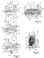
- FIG. 1 is schematically a signal tower 1 according to the invention mounted on a technical device 2, wherein the signal tower 1 via not shown connecting lines of the machine or the device 2 and a corresponding electrical / electronic control receives electrical signals as information regarding the operating conditions of the device 2 receives.
- FIG. 1 illustrates that the signal tower 1 has a modular design, wherein in the illustrated embodiment, the signal tower 1 a total of four lighting modules 3 with bulbs and additionally at the (upper) end an acoustic module 4 for generating acoustic signals and end a final cover 7.
- the signal tower 1 or the lighting modules 3 are connected via a connection module 5 with a base module 6, wherein the base module 6 is designed for fixing the signal tower 1 on the technical device 2, for example by screw or the like.
- the individual modules 3, 4, 5, 6, 7 are connected in a known manner releasably connected to one another in a known manner by way of a bayonet closure (not shown).
- a bayonet closure not shown
- the individual modules 3, 4, 5, 6, 7 can be mounted or fixed in a direction of a longitudinal axis 8 in combination with a rotation 9 about the longitudinal axis 8 and disassembled or released again.
- such modules 3, 4, 5, 6, 7 are commonly referred to as so-called "change modules", as they can be easily quickly replaced, that is without the use of tools, quickly replaced or assembled and disassembled.
- FIG. 2 is the signal tower 1 according to FIG. 1 shown in a cutaway view.
- printed circuit boards 11 and so-called boards 11 of the lighting modules 3, acoustic module 4 and connection module 5 shown.
- the connection module 5 has a printed circuit board 11, on which a connection terminal 12 is fixed or arranged. With the help of this terminal 12 not shown electrical wires coming from the device 2 and connected through the base module 6 going or clamped.
- the printed circuit boards 11 of the lighting modules 3 have advantageous light sources 10, preferably LEDs 10.
- the acoustic module 4 has a printed circuit board 11, which has an acoustic element, not shown in detail, in particular a piezo buzzer or the like, so that an acoustic signaling can be realized.
- FIG. 2 it is illustrated that the printed circuit boards 11 or sinkers 11 in the mounted operating position are arranged essentially in alignment in the direction of the longitudinal axis 8 one behind the other or in / on a longitudinal center plane 29 of the signal tower 1.
- the longitudinal center plane 29 corresponds here in FIG FIG. 2 the viewing / leaf level or lies parallel to the sheet level.
- contact elements 14 or contact springs 14 or leaf spring contacts 14 are provided in the mounted operating position between the printed circuit boards 11 which are arranged in the longitudinal direction 8 for electrical contacting.
- the contacting between the circuit boards 11 by means of the contact springs 14 in such a way that the circuit boards 11 at a first, in particular based on the structure of the signal tower 1 "upper" end 15 lateral contact surfaces 17, for example as Solder contacts are formed.
- These contact surfaces 17 are located in an advantageous manner on a side surface / plane or on the two opposite side surfaces of the printed circuit board 11.
- the side surfaces or contact surfaces 17 are aligned in an advantageous manner in the longitudinal direction 8 and / or arranged parallel to the longitudinal center plane 29.
- the respective circuit board 11 is permanently connected to a separate contact element 14 and a separate contact spring 14 in operation.
- the contact spring 14 has for contacting with an adjacent circuit board 11, a contact surface 18, that is, a so-called second contact surface 18 in the sense of the invention.
- the contact surface 18 is in particular in the Figures 10 and 11 more clearly visible.
- a contact 32 according to the invention between two printed circuit boards 11 arranged in the longitudinal direction 8 of two adjacent modules 3, 4, 5, 6 is realized as a detachable contact 32 with the so-called second contact surface 18 and a so-called first contact surface 19.
- the contact surface 19 of the circuit board 11 as the end face 19 and first contact surface 19 is formed.
- the contact surface 19 in an advantageous manner as a front side arranged or mounted solder joint or the like can be realized.
- FIG. 5 is a circuit board 11 shown according to the invention, among other things, the end faces 19 and first contact surfaces 19 are shown in more detail. In addition, connecting lines 20 between the first, front-side contact surfaces 19 and the lateral contact surfaces 17 at the opposite end 15 of the circuit board 11 are shown.
- the circuit board 11 or the circuit board 11 is formed as a connecting line between adjacent modules 3, 4, 5.
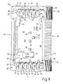
- FIG. 9 clearly, wherein the planar / planar printed circuit boards 11 and the contact springs 14 are freed from other components such as the cap 13 of the signal tower 1, that an aligned in mounted operating position arrangement preferably all circuit boards 11 in the longitudinal direction 8 or on / in the longitudinal center plane 29 provided or ., Is realized, between the aligned in the longitudinal direction 8 / exposed end faces of the circuit boards 11 of the contact according to the invention or the contact surfaces 18 and 19 according to the invention are arranged / realized.
- an advantageous force flow from / in the longitudinal direction 8 or within the longitudinal center plane 29 or the printed circuit board plane can be realized.
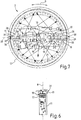
- FIGS. 7 . 9 and 10 clearly that on both side surfaces or longitudinal planes of the circuit board 11 of a lighting module 3 bulbs 10 and LED's 10 are arranged.
- FIG. 7 schematically the radiation directions are exemplified with schematic, individual radiation arrows.
- top LEDs 10 are arranged on the one hand in the central area of the printed circuit board 11 or in the center of the lighting module 3 or the dome 10, emitting light away from the printed circuit board 11 radially outward in a relatively large angular range .
- side LEDs 10 are arranged, which emit light partly in parallel and partially at an acute angle to the printed circuit board 11 (see schematic light arrows).
- the dome 13 has on its inside an advantageous internal corrugation 21.
- the inner corrugation is preferably formed as a round or semicircular inner corrugation 21.
- an advantageous light scattering can be realized.
- external corrugation 22 is preferably formed jagged or triangular.
- an inner corrugation 21 aligned in the longitudinal direction 8 is provided, in particular an inner corrugation 21 formed with a semicircular cross-section, which can be generated in an advantageous manner by injection molding or correspondingly advantageous injection molding tools.
- an external corrugation 22 arranged transversely to the longitudinal axis 8 or perpendicular / orthogonal to the longitudinal axis 8, in particular a jagged or triangular outer corrugation 22, can likewise be generated with the aid of an advantageous injection molding technique or, for example, with the aid of two injection half-shell elements.
- the frontal base surface 24 may be formed integrally with the hollow cylindrical cap 13, in particular by injection molding of plastic material.
- a module 3, 4, 5 which has a separate (hollow cylindrical) cap 13, in particular made of transparent or semitransparent and / or milky plastic material, with a separate base 24 or end face made of opaque material and / or be realized with an opaque coating / occupancy.
- an integral unit of frontal base 24 is provided with hollow cylindrical cap 13 made of at least transparent / translucent material, wherein on the frontal base surface 24 a opaque layer / occupancy is arranged.
- This opaque layer / occupancy of the base 24 is preferably designed as a sticker with advantageous information / information on, for example, the product, the manufacturer, the usability or technical properties / qualities or test certificates of the module 3, 4, 5, 6, 7.
- FIG. 6 are two, in the assembled state adjacent printed circuit boards 11, but shown without the operation to be arranged therebetween contact springs 14. This particularly illustrates the arrangement of the contact surfaces 17 and the frontal contact surfaces 19 of the respective adjacent printed circuit boards 11 of the corresponding adjacent modules 3, 4, 5 or lighting modules 3.
- the contact springs 14 are preferably made of metal, in particular resilient, elastic metal.
- the contact springs 14 are preferably made of metal, in particular resilient, elastic metal.
- the acoustic module 4 or connection module 5 are in operative connection and ensure a permanent, secure or fixed latching / fixing.
- an advantageous assembly of the module 3, 4, 5 can be realized.
- a printed circuit board 11 or a holding web 31 of the printed circuit board 11 is held by means of holders 26 and / or a guide groove or holding groove 30 of the calotte 13.
- the circuit board 11 is inserted in the direction of the longitudinal axis 8 in the module 3, 4, 5, so that a radially defined arrangement or a holding the circuit board 11 is realized by the cap 13 at least at a first end 16.
- a fixed fixation of the printed circuit board 11 (at the end 15), in particular in the longitudinal direction 8, is realized by the advantageous mounting of the spring contacts 14 in the recesses 25 of the base 24.
- the spring contacts 14 and contact springs 14 are firmly locked or fixed by the locking lugs 23 with the base 24 and the cap 13.
- a secure contacting of the printed circuit board 11 or the contact surface 17 with the contact spring 14 is realized by the contact lip 27.
- the contact springs 14 in any manner, that is in particular in two different, offset by 180 ° positions / mounting positions, respectively in the corresponding recess 25 can be pushed or latched into it, without any disadvantageous fixing or contacting would be connected thereto.
- the circuit board 11 in an advantageous manner according to both opposite longitudinal sides or planes accordingly advantageous contact surfaces 17 for contacting with the contact springs 14. Accordingly, a person or a robot or an assembly machine when manufacturing the module 3, 4, 5 need not pay attention to the correct installation position of the contact springs 14, since there are two correct or equivalent installation positions, which is a significant simplification / improvement of the manufacturing effort ,
- the two contact surfaces 18, 19, which realize the detachable contact 32 according to the invention between the modules 3, 4, 5 and the end sides of the printed circuit boards 11, are aligned substantially perpendicular or orthogonal to the longitudinal axis 8.
- the contact springs 14 each have two ramps 28 arranged at an acute angle to the second contact surface 18.
- ramps 28 are advantageously suitable for example with a bayonet closure between adjacent modules 3, 4, 5, 6, 7 by the transverse adjustment or the rotational movement in direction 9 (relative movement between two adjacent modules 3, 4, 5, 6 , 7) a printed circuit board 11 or arranged on the front side / existing first contact surfaces 19 along the ramps 28 to the second contact surface 18 of the spring contact 14 are advantageously adjustable.
- the contact springs 14 are preferably arranged in the non-contacted state that when contacting or in a lateral or rotary adjustment of adjacent modules 3, 4, 5, 6, 7, the contact springs 14 in an advantageous manner (using the ramps 28) in Direction of the longitudinal axis 8 realize a certain travel.
- an advantageous spring force or contact force in the longitudinal direction 8 is generated, which ensures a secure electrical contact, and on the other hand, this assembly and / or manufacturing tolerances can be compensated, for example, the frontal contacts or solder contacts of a printed circuit board 11.
- FIG. 11a a first joining position or mounting position shown, wherein of a first module 3, 4, 5, a first circuit board 11 (at the "upper" part of FIG. 11a shown, without representation of the cap 13) at an acute angle to a contact strip with a row of the contact elements 14 and an adjacent second circuit board 11 of a second module 3, 4, 5, 6 is arranged.
- FIG. 11a a first joining position or mounting position shown, wherein of a first module 3, 4, 5, a first circuit board 11 (at the "upper" part of FIG. 11a shown, without representation of the cap 13) at an acute angle to a contact strip with a row of the contact elements 14 and an adjacent second circuit board 11 of a second module 3, 4, 5, 6 is arranged.
- the first (upper) circuit board 11 is aligned / shown at a smaller angle to the second (lower) circuit board 11, and finally according to FIG. 11c the two circuit boards 11 are arranged in the operating position substantially parallel or in alignment with each other or on the longitudinal center plane 29.
- FIG. 10 different intermediate stages and the assembled end position of a contacting system according to the invention or a signal tower 1 according to the invention is also in FIG. 10 represented, with the circuit boards 11 and contact springs 14 are shown without corresponding dome, ie freed to better illustrate the different joining positions. So is in the upper part of the FIG. 10 the end position or the mounted operating position between adjacent modules 3, 4, 5, 6 or adjacent printed circuit boards 11 shown with the contact springs 14 and in the lower part of FIG. 10 is an intermediate position immediately after the axial assembly or adjustment of two adjacent modules 3, 4, 5, 6, in particular of the connection module with the terminal 12 and a adjacent lighting module 3 shown.
- this lower representation represents the intermediate position in the case of a bayonet closure, wherein in a first joining step a relative adjustment of two adjacent modules 3, 4, 5, 6, 7 takes place in the longitudinal direction 8 and then a transverse adjustment or rotation 9 takes place about the longitudinal axis 8, like this in the middle area of the FIG. 10 is illustrated as an intermediate position.
- This rotation 9 is preferably carried out to the end position according to the upper illustration in FIG FIG. 10 or according to FIG. 11c or FIG. 9 , wherein the two circuit boards 11 are arranged in the operating position substantially parallel or in alignment with each other or on the longitudinal center plane 29.
- the circuit board 11 in the so-called "longitudinal center plane" 29 of a module 3 and a cap 13 is arranged or positioned / fixed.
- This longitudinal center plane 29 extends along the longitudinal axis 8 over an entire signal tower 1, wherein substantially all printed circuit boards 11 are arranged in alignment in the longitudinal center plane 29.
- the contact surfaces 18, 19 of the contact according to the invention are arranged according to the invention.
- an advantageous contact strip is realized by the arrangement of all contact springs 14 along the longitudinal center plane 29 or orthogonal to the longitudinal axis 8.
- This contact strip is formed symmetrically in an advantageous manner, which is advantageous, for example, when using a bayonet closure, not shown, for the tool-less detachable connection of adjacent modules 3, 4, 5, 6, 7 (cf., inter alia Figures 10 and 11 ).
- the contacting according to the invention of adjacent modules 3, 4, 5, 6, 7 not only with an adjustment of adjacent modules 3, 4, 5, 6, 7 takes place in the longitudinal direction 8, but that alternatively or in combination thereto, an adjustment transverse to the longitudinal axis 8 is present.
- a rotation 9 is provided about the longitudinal axis 8.
- a sliding contact or a realization of the contact 32 according to the invention with the two contact surfaces 18, 19 is realized as sliding contact.
- the contact surfaces 18, 19 are oriented transversely or orthogonally to the longitudinal axis 8 in an advantageous manner.
- this contacting according to the invention not only high demands on the electrical power supply or power supply between adjacent modules are met, but rather can be arranged with the contacting system according to the invention on separate electrical connecting wires or lines, for example on the inside of the cap 13, be omitted in order to realize a "looping through” the power supply or power supply.
- an advantageous uniform and / or closed base area 24 can also be realized with such an advantageous areal contacting, which is preferably arranged essentially transversely or orthogonally to the longitudinal axis on the base area 24.
- advantageous sealing elements or elastomer seals may be provided on the spring contacts 14 or in the recesses 25 for this purpose.
- a seal between the modules 3, 4, 5, 6, 7 can be provided, being provided on the calotte 13 in the region of the base 24 externally arranged O-rings or the like. This is particularly advantageous in applications with moist air or in damp rooms or the like.
Landscapes
- Physics & Mathematics (AREA)
- Engineering & Computer Science (AREA)
- General Engineering & Computer Science (AREA)
- General Physics & Mathematics (AREA)
- Electromagnetism (AREA)
- Arrangement Of Elements, Cooling, Sealing, Or The Like Of Lighting Devices (AREA)
- Coupling Device And Connection With Printed Circuit (AREA)
- Connector Housings Or Holding Contact Members (AREA)
Applications Claiming Priority (1)
| Application Number | Priority Date | Filing Date | Title |
|---|---|---|---|
| DE102015120280.8A DE102015120280A1 (de) | 2015-11-24 | 2015-11-24 | Signalgerät mit Leuchtmodul |
Publications (2)
| Publication Number | Publication Date |
|---|---|
| EP3174021A1 EP3174021A1 (de) | 2017-05-31 |
| EP3174021B1 true EP3174021B1 (de) | 2019-09-18 |
Family
ID=57067909
Family Applications (1)
| Application Number | Title | Priority Date | Filing Date |
|---|---|---|---|
| EP16181041.1A Active EP3174021B1 (de) | 2015-11-24 | 2016-07-25 | Signalgerät mit leuchtmodul |
Country Status (5)
| Country | Link |
|---|---|
| US (1) | US10134246B2 (zh) |
| EP (1) | EP3174021B1 (zh) |
| JP (1) | JP6389226B2 (zh) |
| CN (1) | CN106971472B (zh) |
| DE (1) | DE102015120280A1 (zh) |
Families Citing this family (8)
| Publication number | Priority date | Publication date | Assignee | Title |
|---|---|---|---|---|
| USD898600S1 (en) * | 2017-07-20 | 2020-10-13 | Mallory Sonalert Products, Inc. | Stack light |
| CN108019640B (zh) * | 2018-01-09 | 2024-05-03 | 浙江双科电气有限公司 | 一种多层警示灯模块 |
| DE202018105186U1 (de) | 2018-09-11 | 2018-09-20 | Werma Holding Gmbh + Co. Kg | Optisches Signalgerät mit einer Kalotte und einem Abschlusselement |
| CN112361240B (zh) * | 2020-10-14 | 2022-11-08 | 苏州地枢新材料科技有限公司 | 一种便于维修的行人警示立柱一体机 |
| WO2023277784A1 (en) * | 2021-06-29 | 2023-01-05 | Schneider Electric Asia Pte Ltd | Tower signal module |
| DE102021133541A1 (de) * | 2021-12-16 | 2023-06-22 | Reto Zimmermann | Signalpfosten |
| DE102022134962A1 (de) | 2022-02-02 | 2023-08-03 | Werma Holding Gmbh + Co. Kg | Kontaktierungssystem Anschlusselement |
| DE102022120552A1 (de) | 2022-08-15 | 2024-02-15 | Werma Holding Gmbh + Co. Kg | Signalgerät |
Family Cites Families (25)
| Publication number | Priority date | Publication date | Assignee | Title |
|---|---|---|---|---|
| JPS5028246U (zh) * | 1973-07-05 | 1975-04-01 | ||
| JPS5028246A (zh) | 1973-07-12 | 1975-03-22 | ||
| JPS6079681A (ja) * | 1983-09-28 | 1985-05-07 | モレツクス・インコ−ポレ−テツド | ヒンジ付電気コネクタ− |
| US4779803A (en) | 1986-08-11 | 1988-10-25 | Calmar, Inc. | Manually actuated liquid sprayer |
| JPS6349269U (zh) * | 1986-09-17 | 1988-04-04 | ||
| JPH0267568U (zh) * | 1988-11-11 | 1990-05-22 | ||
| JPH0758509B2 (ja) | 1989-06-02 | 1995-06-21 | 三菱電機株式会社 | 図形ぬりつぶし装置 |
| JPH036675U (zh) * | 1989-06-05 | 1991-01-23 | ||
| JPH0631604Y2 (ja) * | 1989-11-10 | 1994-08-22 | アロー電子工業株式会社 | 表示灯 |
| JP4083277B2 (ja) | 1998-03-03 | 2008-04-30 | アビックス株式会社 | Ledイルミネーション器具 |
| DE19854666C2 (de) | 1998-11-26 | 2003-01-02 | Schneider Electric Gmbh | Signaleinrichtung |
| FR2794217B1 (fr) * | 1999-05-28 | 2001-07-20 | Schneider Electric Ind Sa | Element de colonne lumineuse |
| DE10041202A1 (de) | 2000-08-23 | 2002-03-21 | Lmg Signaltechnologie Kg | Signalsäule |
| DE10212895A1 (de) * | 2002-03-22 | 2003-10-02 | Werma Signaltechnik Gmbh & Co | Signalsäule |
| JP4134748B2 (ja) | 2003-02-21 | 2008-08-20 | 株式会社パトライト | 信号表示灯用ユニットおよび信号表示灯 |
| DE10316512A1 (de) | 2003-04-09 | 2004-10-21 | Werma Signaltechnik Gmbh + Co. Kg | Signalgerät |
| US20060262533A1 (en) * | 2005-05-18 | 2006-11-23 | Para Light Electronics Co., Ltd. | Modular light emitting diode |
| AU2008201153C1 (en) * | 2007-03-28 | 2011-01-06 | Aristocrat Technologies Australia Pty Limited | A Modular Visual Output Component |
| US8132935B2 (en) * | 2008-09-01 | 2012-03-13 | Samsung Led Co., Ltd. | Light emitting module |
| JP2012014967A (ja) * | 2010-07-01 | 2012-01-19 | Toshiba Lighting & Technology Corp | 端子装置、電気装置、電気機器および照明器具 |
| US8057263B1 (en) * | 2010-07-12 | 2011-11-15 | Tyco Electronics Corporation | Edge connectors having stamped signal contacts |
| JP5499071B2 (ja) * | 2012-04-17 | 2014-05-21 | シャープ株式会社 | 中継コネクタ及びこれを備える光源モジュール |
| US20150198317A1 (en) * | 2014-01-13 | 2015-07-16 | Rockwell Automation Technologies, Inc. | Stack Light with Modular Power Converter |
| US9307309B2 (en) * | 2014-01-13 | 2016-04-05 | Rockwell Automation Technologies, Inc. | Stack light with in-line sound module |
| PL3043111T3 (pl) * | 2015-01-12 | 2017-09-29 | Auer Signal Gmbh | Urządzenie sygnalizacyjne |
-
2015
- 2015-11-24 DE DE102015120280.8A patent/DE102015120280A1/de not_active Withdrawn
-
2016
- 2016-07-25 EP EP16181041.1A patent/EP3174021B1/de active Active
- 2016-11-22 US US15/359,565 patent/US10134246B2/en active Active
- 2016-11-22 CN CN201611031870.0A patent/CN106971472B/zh active Active
- 2016-11-24 JP JP2016228220A patent/JP6389226B2/ja active Active
Non-Patent Citations (1)
| Title |
|---|
| None * |
Also Published As
| Publication number | Publication date |
|---|---|
| US10134246B2 (en) | 2018-11-20 |
| JP2017098252A (ja) | 2017-06-01 |
| JP6389226B2 (ja) | 2018-09-12 |
| DE102015120280A1 (de) | 2017-05-24 |
| CN106971472B (zh) | 2019-06-28 |
| CN106971472A (zh) | 2017-07-21 |
| US20170148283A1 (en) | 2017-05-25 |
| EP3174021A1 (de) | 2017-05-31 |
Similar Documents
| Publication | Publication Date | Title |
|---|---|---|
| EP3174021B1 (de) | Signalgerät mit leuchtmodul | |
| DE4243175B4 (de) | Beleuchtungseinrichtung | |
| DE102008005823B4 (de) | Anschlusselement zur elektrischen Anbindung einer LED | |
| EP1405377B1 (de) | Led-modul für beleuchtungsvorrichtungen | |
| EP1347233B1 (de) | Signalsäule | |
| DE102013111578B4 (de) | Elektronikmodul | |
| AT14657U1 (de) | Leuchte mit auswechselbaren Leuchtmodulen | |
| DE10111594A1 (de) | Anzeigeleuchtensäule | |
| EP3006816A1 (de) | Längliche led-leuchte mit optischem element | |
| AT14620U1 (de) | Leuchte mit Trägerelement und lösbar befestigbarem Leuchtmodul | |
| DE102012023190A1 (de) | Signalsäule | |
| EP3114400A1 (de) | Leuchte bzw. beleuchtungsanordnung mit länglichem trägerelement und lösbar befestigbarem leuchtmodul | |
| DE19722925C1 (de) | Elektrisches Anschlußelement für Elektromagnete von Ventileinheiten | |
| EP3056805A1 (de) | Langgestreckte optik für led-module | |
| DE202015106381U1 (de) | Signalgerät mit Leuchtmodul | |
| EP3165821B1 (de) | Längliches lichtbandelement | |
| DE102011122530A1 (de) | "Warnleuchtsäule mit einem elektrischen Kontakt zwischen zwei Wechselmodulen" | |
| EP3171078B1 (de) | Led-lichtquelle | |
| EP2694874A1 (de) | Vorrichtung zum befestigen und kontaktieren eines leuchtmittels und/oder eines leuchtmoduls, sowie leuchte | |
| EP3477190A1 (de) | Optisches system für eine led leuchte | |
| DE202012011371U1 (de) | Signalsäule | |
| DE202012103061U1 (de) | Leuchtmodul und Leuchtsystem mit Leuchtmodul | |
| DE202018105186U1 (de) | Optisches Signalgerät mit einer Kalotte und einem Abschlusselement | |
| EP4224634A1 (de) | Kontaktierungssystem anschlusselement | |
| DE3346594C2 (zh) |
Legal Events
| Date | Code | Title | Description |
|---|---|---|---|
| PUAI | Public reference made under article 153(3) epc to a published international application that has entered the european phase |
Free format text: ORIGINAL CODE: 0009012 |
|
| STAA | Information on the status of an ep patent application or granted ep patent |
Free format text: STATUS: THE APPLICATION HAS BEEN PUBLISHED |
|
| AK | Designated contracting states |
Kind code of ref document: A1 Designated state(s): AL AT BE BG CH CY CZ DE DK EE ES FI FR GB GR HR HU IE IS IT LI LT LU LV MC MK MT NL NO PL PT RO RS SE SI SK SM TR |
|
| AX | Request for extension of the european patent |
Extension state: BA ME |
|
| STAA | Information on the status of an ep patent application or granted ep patent |
Free format text: STATUS: REQUEST FOR EXAMINATION WAS MADE |
|
| 17P | Request for examination filed |
Effective date: 20170608 |
|
| RBV | Designated contracting states (corrected) |
Designated state(s): AL AT BE BG CH CY CZ DE DK EE ES FI FR GB GR HR HU IE IS IT LI LT LU LV MC MK MT NL NO PL PT RO RS SE SI SK SM TR |
|
| RIC1 | Information provided on ipc code assigned before grant |
Ipc: F21V 23/06 20060101ALI20190422BHEP Ipc: G08B 5/36 20060101AFI20190422BHEP |
|
| GRAP | Despatch of communication of intention to grant a patent |
Free format text: ORIGINAL CODE: EPIDOSNIGR1 |
|
| STAA | Information on the status of an ep patent application or granted ep patent |
Free format text: STATUS: GRANT OF PATENT IS INTENDED |
|
| INTG | Intention to grant announced |
Effective date: 20190607 |
|
| GRAS | Grant fee paid |
Free format text: ORIGINAL CODE: EPIDOSNIGR3 |
|
| GRAA | (expected) grant |
Free format text: ORIGINAL CODE: 0009210 |
|
| STAA | Information on the status of an ep patent application or granted ep patent |
Free format text: STATUS: THE PATENT HAS BEEN GRANTED |
|
| AK | Designated contracting states |
Kind code of ref document: B1 Designated state(s): AL AT BE BG CH CY CZ DE DK EE ES FI FR GB GR HR HU IE IS IT LI LT LU LV MC MK MT NL NO PL PT RO RS SE SI SK SM TR |
|
| REG | Reference to a national code |
Ref country code: GB Ref legal event code: FG4D Free format text: NOT ENGLISH |
|
| REG | Reference to a national code |
Ref country code: CH Ref legal event code: EP |
|
| REG | Reference to a national code |
Ref country code: DE Ref legal event code: R096 Ref document number: 502016006657 Country of ref document: DE |
|
| REG | Reference to a national code |
Ref country code: AT Ref legal event code: REF Ref document number: 1182222 Country of ref document: AT Kind code of ref document: T Effective date: 20191015 |
|
| REG | Reference to a national code |
Ref country code: IE Ref legal event code: FG4D Free format text: LANGUAGE OF EP DOCUMENT: GERMAN |
|
| REG | Reference to a national code |
Ref country code: NL Ref legal event code: MP Effective date: 20190918 |
|
| PG25 | Lapsed in a contracting state [announced via postgrant information from national office to epo] |
Ref country code: FI Free format text: LAPSE BECAUSE OF FAILURE TO SUBMIT A TRANSLATION OF THE DESCRIPTION OR TO PAY THE FEE WITHIN THE PRESCRIBED TIME-LIMIT Effective date: 20190918 Ref country code: BG Free format text: LAPSE BECAUSE OF FAILURE TO SUBMIT A TRANSLATION OF THE DESCRIPTION OR TO PAY THE FEE WITHIN THE PRESCRIBED TIME-LIMIT Effective date: 20191218 Ref country code: NO Free format text: LAPSE BECAUSE OF FAILURE TO SUBMIT A TRANSLATION OF THE DESCRIPTION OR TO PAY THE FEE WITHIN THE PRESCRIBED TIME-LIMIT Effective date: 20191218 Ref country code: SE Free format text: LAPSE BECAUSE OF FAILURE TO SUBMIT A TRANSLATION OF THE DESCRIPTION OR TO PAY THE FEE WITHIN THE PRESCRIBED TIME-LIMIT Effective date: 20190918 Ref country code: LT Free format text: LAPSE BECAUSE OF FAILURE TO SUBMIT A TRANSLATION OF THE DESCRIPTION OR TO PAY THE FEE WITHIN THE PRESCRIBED TIME-LIMIT Effective date: 20190918 Ref country code: HR Free format text: LAPSE BECAUSE OF FAILURE TO SUBMIT A TRANSLATION OF THE DESCRIPTION OR TO PAY THE FEE WITHIN THE PRESCRIBED TIME-LIMIT Effective date: 20190918 |
|
| REG | Reference to a national code |
Ref country code: LT Ref legal event code: MG4D |
|
| PG25 | Lapsed in a contracting state [announced via postgrant information from national office to epo] |
Ref country code: AL Free format text: LAPSE BECAUSE OF FAILURE TO SUBMIT A TRANSLATION OF THE DESCRIPTION OR TO PAY THE FEE WITHIN THE PRESCRIBED TIME-LIMIT Effective date: 20190918 Ref country code: RS Free format text: LAPSE BECAUSE OF FAILURE TO SUBMIT A TRANSLATION OF THE DESCRIPTION OR TO PAY THE FEE WITHIN THE PRESCRIBED TIME-LIMIT Effective date: 20190918 Ref country code: GR Free format text: LAPSE BECAUSE OF FAILURE TO SUBMIT A TRANSLATION OF THE DESCRIPTION OR TO PAY THE FEE WITHIN THE PRESCRIBED TIME-LIMIT Effective date: 20191219 Ref country code: LV Free format text: LAPSE BECAUSE OF FAILURE TO SUBMIT A TRANSLATION OF THE DESCRIPTION OR TO PAY THE FEE WITHIN THE PRESCRIBED TIME-LIMIT Effective date: 20190918 |
|
| PG25 | Lapsed in a contracting state [announced via postgrant information from national office to epo] |
Ref country code: EE Free format text: LAPSE BECAUSE OF FAILURE TO SUBMIT A TRANSLATION OF THE DESCRIPTION OR TO PAY THE FEE WITHIN THE PRESCRIBED TIME-LIMIT Effective date: 20190918 Ref country code: PL Free format text: LAPSE BECAUSE OF FAILURE TO SUBMIT A TRANSLATION OF THE DESCRIPTION OR TO PAY THE FEE WITHIN THE PRESCRIBED TIME-LIMIT Effective date: 20190918 Ref country code: PT Free format text: LAPSE BECAUSE OF FAILURE TO SUBMIT A TRANSLATION OF THE DESCRIPTION OR TO PAY THE FEE WITHIN THE PRESCRIBED TIME-LIMIT Effective date: 20200120 Ref country code: ES Free format text: LAPSE BECAUSE OF FAILURE TO SUBMIT A TRANSLATION OF THE DESCRIPTION OR TO PAY THE FEE WITHIN THE PRESCRIBED TIME-LIMIT Effective date: 20190918 Ref country code: NL Free format text: LAPSE BECAUSE OF FAILURE TO SUBMIT A TRANSLATION OF THE DESCRIPTION OR TO PAY THE FEE WITHIN THE PRESCRIBED TIME-LIMIT Effective date: 20190918 Ref country code: RO Free format text: LAPSE BECAUSE OF FAILURE TO SUBMIT A TRANSLATION OF THE DESCRIPTION OR TO PAY THE FEE WITHIN THE PRESCRIBED TIME-LIMIT Effective date: 20190918 |
|
| PG25 | Lapsed in a contracting state [announced via postgrant information from national office to epo] |
Ref country code: SK Free format text: LAPSE BECAUSE OF FAILURE TO SUBMIT A TRANSLATION OF THE DESCRIPTION OR TO PAY THE FEE WITHIN THE PRESCRIBED TIME-LIMIT Effective date: 20190918 Ref country code: CZ Free format text: LAPSE BECAUSE OF FAILURE TO SUBMIT A TRANSLATION OF THE DESCRIPTION OR TO PAY THE FEE WITHIN THE PRESCRIBED TIME-LIMIT Effective date: 20190918 Ref country code: SM Free format text: LAPSE BECAUSE OF FAILURE TO SUBMIT A TRANSLATION OF THE DESCRIPTION OR TO PAY THE FEE WITHIN THE PRESCRIBED TIME-LIMIT Effective date: 20190918 Ref country code: IS Free format text: LAPSE BECAUSE OF FAILURE TO SUBMIT A TRANSLATION OF THE DESCRIPTION OR TO PAY THE FEE WITHIN THE PRESCRIBED TIME-LIMIT Effective date: 20200224 |
|
| REG | Reference to a national code |
Ref country code: DE Ref legal event code: R097 Ref document number: 502016006657 Country of ref document: DE |
|
| PLBE | No opposition filed within time limit |
Free format text: ORIGINAL CODE: 0009261 |
|
| STAA | Information on the status of an ep patent application or granted ep patent |
Free format text: STATUS: NO OPPOSITION FILED WITHIN TIME LIMIT |
|
| PG2D | Information on lapse in contracting state deleted |
Ref country code: IS |
|
| PG25 | Lapsed in a contracting state [announced via postgrant information from national office to epo] |
Ref country code: DK Free format text: LAPSE BECAUSE OF FAILURE TO SUBMIT A TRANSLATION OF THE DESCRIPTION OR TO PAY THE FEE WITHIN THE PRESCRIBED TIME-LIMIT Effective date: 20190918 Ref country code: IS Free format text: LAPSE BECAUSE OF FAILURE TO SUBMIT A TRANSLATION OF THE DESCRIPTION OR TO PAY THE FEE WITHIN THE PRESCRIBED TIME-LIMIT Effective date: 20200119 |
|
| 26N | No opposition filed |
Effective date: 20200619 |
|
| PG25 | Lapsed in a contracting state [announced via postgrant information from national office to epo] |
Ref country code: SI Free format text: LAPSE BECAUSE OF FAILURE TO SUBMIT A TRANSLATION OF THE DESCRIPTION OR TO PAY THE FEE WITHIN THE PRESCRIBED TIME-LIMIT Effective date: 20190918 |
|
| PG25 | Lapsed in a contracting state [announced via postgrant information from national office to epo] |
Ref country code: MC Free format text: LAPSE BECAUSE OF FAILURE TO SUBMIT A TRANSLATION OF THE DESCRIPTION OR TO PAY THE FEE WITHIN THE PRESCRIBED TIME-LIMIT Effective date: 20190918 |
|
| REG | Reference to a national code |
Ref country code: CH Ref legal event code: PL |
|
| REG | Reference to a national code |
Ref country code: BE Ref legal event code: MM Effective date: 20200731 |
|
| PG25 | Lapsed in a contracting state [announced via postgrant information from national office to epo] |
Ref country code: CH Free format text: LAPSE BECAUSE OF NON-PAYMENT OF DUE FEES Effective date: 20200731 Ref country code: LI Free format text: LAPSE BECAUSE OF NON-PAYMENT OF DUE FEES Effective date: 20200731 Ref country code: LU Free format text: LAPSE BECAUSE OF NON-PAYMENT OF DUE FEES Effective date: 20200725 |
|
| PG25 | Lapsed in a contracting state [announced via postgrant information from national office to epo] |
Ref country code: BE Free format text: LAPSE BECAUSE OF NON-PAYMENT OF DUE FEES Effective date: 20200731 |
|
| PG25 | Lapsed in a contracting state [announced via postgrant information from national office to epo] |
Ref country code: IE Free format text: LAPSE BECAUSE OF NON-PAYMENT OF DUE FEES Effective date: 20200725 |
|
| PG25 | Lapsed in a contracting state [announced via postgrant information from national office to epo] |
Ref country code: TR Free format text: LAPSE BECAUSE OF FAILURE TO SUBMIT A TRANSLATION OF THE DESCRIPTION OR TO PAY THE FEE WITHIN THE PRESCRIBED TIME-LIMIT Effective date: 20190918 Ref country code: MT Free format text: LAPSE BECAUSE OF FAILURE TO SUBMIT A TRANSLATION OF THE DESCRIPTION OR TO PAY THE FEE WITHIN THE PRESCRIBED TIME-LIMIT Effective date: 20190918 Ref country code: CY Free format text: LAPSE BECAUSE OF FAILURE TO SUBMIT A TRANSLATION OF THE DESCRIPTION OR TO PAY THE FEE WITHIN THE PRESCRIBED TIME-LIMIT Effective date: 20190918 |
|
| PG25 | Lapsed in a contracting state [announced via postgrant information from national office to epo] |
Ref country code: MK Free format text: LAPSE BECAUSE OF FAILURE TO SUBMIT A TRANSLATION OF THE DESCRIPTION OR TO PAY THE FEE WITHIN THE PRESCRIBED TIME-LIMIT Effective date: 20190918 |
|
| REG | Reference to a national code |
Ref country code: AT Ref legal event code: MM01 Ref document number: 1182222 Country of ref document: AT Kind code of ref document: T Effective date: 20210725 |
|
| PG25 | Lapsed in a contracting state [announced via postgrant information from national office to epo] |
Ref country code: AT Free format text: LAPSE BECAUSE OF NON-PAYMENT OF DUE FEES Effective date: 20210725 |
|
| PGFP | Annual fee paid to national office [announced via postgrant information from national office to epo] |
Ref country code: IT Payment date: 20230731 Year of fee payment: 8 Ref country code: GB Payment date: 20230724 Year of fee payment: 8 |
|
| PGFP | Annual fee paid to national office [announced via postgrant information from national office to epo] |
Ref country code: FR Payment date: 20230724 Year of fee payment: 8 Ref country code: DE Payment date: 20230720 Year of fee payment: 8 |