EP3170263B1 - Architektur zur abweisung von nahendblockern und übertragungslecks - Google Patents
Architektur zur abweisung von nahendblockern und übertragungslecks Download PDFInfo
- Publication number
- EP3170263B1 EP3170263B1 EP15739371.1A EP15739371A EP3170263B1 EP 3170263 B1 EP3170263 B1 EP 3170263B1 EP 15739371 A EP15739371 A EP 15739371A EP 3170263 B1 EP3170263 B1 EP 3170263B1
- Authority
- EP
- European Patent Office
- Prior art keywords
- biquad
- signal
- path
- filter
- filtered
- Prior art date
- Legal status (The legal status is an assumption and is not a legal conclusion. Google has not performed a legal analysis and makes no representation as to the accuracy of the status listed.)
- Not-in-force
Links
- 238000001914 filtration Methods 0.000 claims description 42
- 238000000034 method Methods 0.000 claims description 25
- 238000004891 communication Methods 0.000 description 28
- 101100462367 Aspergillus niger (strain CBS 513.88 / FGSC A1513) otaB gene Proteins 0.000 description 7
- 238000013461 design Methods 0.000 description 7
- 238000010586 diagram Methods 0.000 description 6
- 230000006870 function Effects 0.000 description 6
- 230000006872 improvement Effects 0.000 description 5
- 101100462369 Aspergillus niger (strain CBS 513.88 / FGSC A1513) otaC gene Proteins 0.000 description 4
- 230000000903 blocking effect Effects 0.000 description 4
- 239000003990 capacitor Substances 0.000 description 4
- 238000005516 engineering process Methods 0.000 description 4
- 230000015654 memory Effects 0.000 description 4
- 230000003287 optical effect Effects 0.000 description 4
- 230000008569 process Effects 0.000 description 4
- 230000001413 cellular effect Effects 0.000 description 3
- 238000004519 manufacturing process Methods 0.000 description 3
- 229920006395 saturated elastomer Polymers 0.000 description 3
- 238000012546 transfer Methods 0.000 description 3
- 101100462365 Aspergillus niger (strain CBS 513.88 / FGSC A1513) otaA gene Proteins 0.000 description 2
- 230000003321 amplification Effects 0.000 description 2
- 230000008901 benefit Effects 0.000 description 2
- 238000006243 chemical reaction Methods 0.000 description 2
- 238000004590 computer program Methods 0.000 description 2
- 239000000835 fiber Substances 0.000 description 2
- 230000007774 longterm Effects 0.000 description 2
- 238000003199 nucleic acid amplification method Methods 0.000 description 2
- 239000002245 particle Substances 0.000 description 2
- 238000012545 processing Methods 0.000 description 2
- 230000008707 rearrangement Effects 0.000 description 2
- 230000009467 reduction Effects 0.000 description 2
- 238000004088 simulation Methods 0.000 description 2
- 238000013459 approach Methods 0.000 description 1
- 230000005540 biological transmission Effects 0.000 description 1
- 239000003795 chemical substances by application Substances 0.000 description 1
- 230000003750 conditioning effect Effects 0.000 description 1
- 230000000694 effects Effects 0.000 description 1
- 230000000977 initiatory effect Effects 0.000 description 1
- 238000012986 modification Methods 0.000 description 1
- 230000004048 modification Effects 0.000 description 1
- 238000012887 quadratic function Methods 0.000 description 1
- 238000011084 recovery Methods 0.000 description 1
- 238000012360 testing method Methods 0.000 description 1
Images


Classifications
-
- H—ELECTRICITY
- H03—ELECTRONIC CIRCUITRY
- H03H—IMPEDANCE NETWORKS, e.g. RESONANT CIRCUITS; RESONATORS
- H03H11/00—Networks using active elements
- H03H11/02—Multiple-port networks
- H03H11/04—Frequency selective two-port networks
- H03H11/0422—Frequency selective two-port networks using transconductance amplifiers, e.g. gmC filters
- H03H11/0433—Two integrator loop filters
-
- H—ELECTRICITY
- H03—ELECTRONIC CIRCUITRY
- H03H—IMPEDANCE NETWORKS, e.g. RESONANT CIRCUITS; RESONATORS
- H03H11/00—Networks using active elements
- H03H11/02—Multiple-port networks
- H03H11/04—Frequency selective two-port networks
- H03H11/12—Frequency selective two-port networks using amplifiers with feedback
- H03H11/1217—Frequency selective two-port networks using amplifiers with feedback using a plurality of operational amplifiers
- H03H11/1252—Two integrator-loop-filters
-
- H—ELECTRICITY
- H04—ELECTRIC COMMUNICATION TECHNIQUE
- H04B—TRANSMISSION
- H04B1/00—Details of transmission systems, not covered by a single one of groups H04B3/00 - H04B13/00; Details of transmission systems not characterised by the medium used for transmission
- H04B1/06—Receivers
- H04B1/10—Means associated with receiver for limiting or suppressing noise or interference
- H04B1/109—Means associated with receiver for limiting or suppressing noise or interference by improving strong signal performance of the receiver when strong unwanted signals are present at the receiver input
-
- H—ELECTRICITY
- H04—ELECTRIC COMMUNICATION TECHNIQUE
- H04B—TRANSMISSION
- H04B1/00—Details of transmission systems, not covered by a single one of groups H04B3/00 - H04B13/00; Details of transmission systems not characterised by the medium used for transmission
- H04B1/38—Transceivers, i.e. devices in which transmitter and receiver form a structural unit and in which at least one part is used for functions of transmitting and receiving
- H04B1/40—Circuits
- H04B1/50—Circuits using different frequencies for the two directions of communication
- H04B1/52—Hybrid arrangements, i.e. arrangements for transition from single-path two-direction transmission to single-direction transmission on each of two paths or vice versa
- H04B1/525—Hybrid arrangements, i.e. arrangements for transition from single-path two-direction transmission to single-direction transmission on each of two paths or vice versa with means for reducing leakage of transmitter signal into the receiver
Definitions
- the present disclosure relates generally to wireless communication systems, and more particularly to a method for rejecting near end blockers and transmit leakage in a receiver module.
- Wireless communication devices have become smaller and more powerful as well as more capable. Increasingly users rely on wireless communication devices for mobile phone use as well as email and Internet access. At the same time, devices have become smaller in size. Devices such as cellular telephones, personal digital assistants (PDAs), laptop computers, and other similar devices provide reliable service with expanded coverage areas. Such devices may be referred to as mobile stations, stations, access terminals, user terminals, subscriber units, user equipments, and similar terms.
- a wireless communication system may support communication for multiple wireless communication devices at the same time.
- a wireless communication device may communicate with one or more base stations by transmissions on the uplink and downlink.
- Base stations may be referred to as access points, Node Bs, or other similar terms.
- the uplink or reverse link refers to the communication link from the wireless communication device to the base station, while the downlink or forward link refers to the communication from the base station to the wireless communication devices.
- Wireless communication systems may be multiple access systems capable of supporting communication with multiple users by sharing the available system resources, such as bandwidth and transmit power.
- multiple access systems include code division multiple access (CDMA) systems, time division multiple access (TDMA) systems, frequency division multiple access (FDMA) systems, wideband code division multiple access (WCDMA) systems, global system for mobile (GSM) communication systems, enhanced data rates for GSM evolution (EDGE) systems, and orthogonal frequency division multiple access (OFDMA) systems.
- CDMA code division multiple access
- TDMA time division multiple access
- FDMA frequency division multiple access
- WCDMA wideband code division multiple access
- GSM global system for mobile
- EDGE enhanced data rates for GSM evolution
- OFDMA orthogonal frequency division multiple access
- desired signals may be blocked due to an adjacent high strength signal.
- This strong signal may saturate the receive circuitry and block the weaker primary receive signal. This occurs when the front end receive circuitry and automatic gain control (AGC) react to the stronger signal, and reduce the front end amplification. When this happens, the desired primary channel receive signal may be lost in the background noise.
- AGC automatic gain control
- Transmit jammer leakage may be a powerful blocker for the receive path in frequency duplex division (FDD) mode in many bands of a wireless communication system, such as the long-term evolution (LTE) band.
- LTE long-term evolution
- receive spacing may be as little as a few tens of MHz. This spacing leads to receiver front end design challenges as filtering of near end blockers in RF is made nearly impossible due to the lack of high quality (Q) of chip components.
- the transmit jammer may saturate the first stage of the base band (BB) filter in high gain modes in the presence of weak signals, as described above.
- Common filtering techniques such as RC filtering is less effective because the rejection is only a few dBs.
- Embodiments contained in the disclosure provide a method of minimizing transmit signal interference.
- the method includes the steps of: receiving a signal and amplifying the received signal.
- the received signal is then mixed with an intermediate frequency signal to obtain a baseband modulated signal.
- the baseband modulated signal is then first filtered in an RC filter.
- the resulting signal is then divided by a preselected amount and the first divided portion is sent to a main path of a biquad filter, which produces a first stage biquad filtered signal.
- the second portion of the divided signal is sent to an auxiliary path of the biquad filter, and produces a second filtered signal.
- the first and second signals are then recombined and sent to the second stage of the biquad filter, where further filtering takes place.
- a further embodiment provides an apparatus for minimizing transmit signal interference.
- the apparatus includes a front end receiver that includes: an antenna, a low noise amplifier, a transformer, a mixer and an RC filter.
- the apparatus provides a main biquad filtering path and at least one auxiliary biquad filtering path.
- a still further embodiment provides an apparatus for minimizing transmit signal interference, the apparatus comprising: means for receiving a signal; means for amplifying the received signal; means for mixing the received signal with an intermediate frequency signal to obtain a baseband modulated signal; means for filtering the baseband modulated signal in a first filter; means for dividing the first filtered baseband modulated signal by a preselected amount; means for sending a first divided portion of the baseband modulated signal to a main path of a biquad filter, producing a first biquad filtered signal; means for sending a second divided portion of the baseband modulated signal to an auxiliary path of the biquad filter, producing a second biquad filtered signal; means for recombining the first biquad filtered signal with the second biquad filtered signal before a second stage of the biquad filter; and means for filtering the recombined biquad filtered signal in the second stage of the biquad filter.
- a yet further embodiment provides a non-transitory computer readable media that includes program instructions, which when executed by a processor cause the processor to perform a method comprising the steps of: receiving a signal; amplifying that received signal; and then mixing the received signal with an intermediate frequency signal to obtain a baseband modulated signal.
- the baseband modulated signal is then filtered with an RC filter and is then dividing by a preselected amount.
- the first divided portion of the baseband modulated signal is sent to a main path of a biquad filter, and produces a first biquad filtered signal.
- the second divided portion of the baseband modulated signal is sent to an auxiliary path of the biquad filter and produces a second biquad filtered signal.
- the first and second divided signals are then recombined and send to a second stage of the biquad filter.
- the recombined signal is then filtered in the second stage of the biquad filter.
- a component may be, but is not limited to being, a process running on a processor, an integrated circuit, a processor, an object, an executable, a thread of execution, a program, and/or a computer.
- an application running on a computing device and the computing device can be a component.
- One or more components can reside within a process and/or thread of execution and a component may be localized on one computer and/or distributed between two or more computers.
- these components can execute from various computer readable media having various data structures stored thereon.
- the components may communicate by way of local and/or remote processes such as in accordance with a signal having one or more data packets (e.g., data from one component interacting with another component in a local system, distributed system, and/or across a network, such as the Internet, with other systems by way of the signal).
- a signal having one or more data packets (e.g., data from one component interacting with another component in a local system, distributed system, and/or across a network, such as the Internet, with other systems by way of the signal).
- An access terminal may refer to a device providing voice and/or data connectivity to a user.
- An access wireless terminal may be connected to a computing device such as a laptop computer or desktop computer, or it may be a self-contained device such as a cellular telephone.
- An access terminal can also be called a system, a subscriber unit, a subscriber station, mobile station, mobile, remote station, remote terminal, a wireless access point, wireless terminal, user terminal, user agent, user device, or user equipment.
- a wireless terminal may be a subscriber station, wireless device, cellular telephone, PCS telephone, cordless telephone, a Session Initiation Protocol (SIP) phone, a wireless local loop (WLL) station, a personal digital assistant (PDA), a handheld device having wireless connection capability, or other processing device connected to a wireless modem.
- An access point otherwise referred to as a base station or base station controller (BSC), may refer to a device in an access network that communicates over the air-interface, through one or more sectors, with wireless terminals.
- the access point may act as a router between the wireless terminal and the rest of the access network, which may include an Internet Protocol (IP) network, by converting received air-interface frames to IP packets.
- IP Internet Protocol
- the access point also coordinates management of attributes for the air interface.
- various aspects or features described herein may be implemented as a method, apparatus, or article of manufacture using standard programming and/or engineering techniques.
- article of manufacture as used herein is intended to encompass a computer program accessible from any computer-readable device, carrier, or media.
- computer readable media can include but are not limited to magnetic storage devices (e.g., hard disk, floppy disk, magnetic strips%), optical disks ( e.g., compact disk (CD), digital versatile disk (DVD)%), smart cards, and flash memory devices (e.g ., card, stick, key drive%), and integrated circuits such as read-only memories, programmable read-only memories, and electrically erasable programmable read-only memories.
- FIG. 1 illustrates a multiple access wireless communication system 100 according to one aspect.
- An access point 102 includes multiple antenna groups, one including 104 and 106, another including 108 and 110, and an additional one including 112 and 114. In FIG. 1 , only two antennas are shown for each antenna group, however, more or fewer antennas may be utilized for each antenna group.
- Access terminal 116 is in communication with antennas 112 and 114, where antennas 112 and 114 transmit information to access terminal 116 over downlink or forward link 118 and receive information from access terminal 116 over uplink or reverse link 120.
- Access terminal 122 is in communication with antennas 106 and 108, where antennas 106 and 108 transmit information to access terminal 122 over downlink or forward link 124, and receive information from access terminal 122 over uplink or reverse link 126.
- communication link 118, 120, 124, and 126 may use a different frequency for communication.
- downlink or forward link 118 may use a different frequency than that used by uplink or reverse link 120.
- antenna groups are each designed to communicate to access terminals in a sector of the areas covered by access point 102.
- the transmitting antennas of an access point utilize beamforming in order to improve the signal-to-noise ration (SNR) of downlinks or forward links for the different access terminals 116 and 122. Also, an access point using beamforming to transmit to access terminals scattered randomly through its coverage causes less interference to access terminals in neighboring cells than an access point transmitting through a single antenna to all its access terminals.
- SNR signal-to-noise ration
- An access point may be a fixed station used for communicating with the terminals and may also be referred to as a Node B, an evolved Node B (eNB), or some other terminology.
- An access terminal may also be called a mobile station, user equipment (UE), a wireless communication device, terminal or some other terminology.
- UE user equipment
- either the AP 102, or the access terminals 116, 122 may utilize the techniques described below to improve performance of the system.
- FIG. 2 shows a block diagram of an exemplary design of a wireless communication device 200.
- wireless device 200 includes a data processor 210 and a transceiver 220.
- Transceiver 220 includes a transmitter 230 and a receiver 250 that support bi-directional wireless communication.
- wireless device 200 may include any number of transmitters and any number of receivers for any number of communication systems and any number of frequency bands.
- data processor 210 processes data to be transmitted and provides an analog output signal to transmitter 230.
- the analog output signal is amplified by an amplifier (Amp) 232, filtered by a lowpass filter 234 to remove images caused by digital-to-analog conversion, amplified by a VGA 236, and upconverted from baseband to RF by a mixer 238.
- the upconverted signal is filtered by a filter 240, further amplified by a driver amplifier, 242 and a power amplifier 244, routed through switches/duplexers 246, and transmitted via an antenna 249.
- antenna 248 receives signals from base stations and/or other transmitter stations and provides a received signal, which is routed through switches/duplexers 246 and provided to receiver 250.
- the received signal is amplified by an LNA 252, filtered by a bandpass filter 254, and downconverted from RF to baseband by a mixer 256.
- the downconverted signal is amplified by a VGA 258, filtered by a lowpass filter 260, and amplified by an amplifier 262 to obtain an analog input signal, which is provided to data processor 210.
- FIG. 2 shows transmitter 230 and receiver 250 implementing a direct-conversion architecture, which frequency converts a signal between RF and baseband in one stage.
- Transmitter 230 and/or receiver 250 may also implement a super-heterodyne architecture, which frequency converts a signal between RF and baseband in multiple stages.
- a local oscillator (LO) generator 270 generates and provides transmit and receive LO signals to mixers 238 and 256, respectively.
- a phase locked loop (PLL) 272 receives control information from data processor 210 and provides control signals to LO generator 270 to generate the transmit and receive LO signals at the proper frequencies.
- LO local oscillator
- PLL phase locked loop
- FIG. 2 shows an exemplary transceiver design.
- the conditioning of the signals in transmitter 230 and receiver 250 may be performed by one or more stages of amplifier, filter, mixer, etc. These circuits may be arranged differently from the configuration shown in FIG. 2 . Some circuits in FIG. 2 may also be omitted. All or a portion of transceiver 220 may be implemented on one or more analog integrated circuits (ICs), RF ICs (RFICs), mixed-signal ICs, etc.
- ICs analog integrated circuits
- RFICs RF ICs
- mixed-signal ICs etc.
- amplifier 232 through power amplifier 244 in transmitter 230 may also be implemented on an RFIC.
- Driver amplifier 242 and power amplifier 244 may also be implemented on another IC external to the RFIC.
- Data processor 210 may perform various functions for wireless device 200, e.g., processing for transmitter and received data.
- Memory 212 may store program codes and data for data processor 210.
- Data processor 210 may be implemented on one or more application specific integrated circuits (ASICs) and/or other ICs.
- ASICs application specific integrated circuits
- This transmit jammer leakage is a powerful blocker of the desired RF path, particularly in FDD mode.
- frequency spacing may be as few as 10 MHz.
- LTE band 12 which requires receiver front end design to be capable of handling spacing of 30 MHz, or LTE band 2 with a 45 MHz spacing.
- This poses significant design challenges as filtering of these near end blocking signals requires quality filters. Providing quality filters is also difficult as filtering of near end blocking signals is further complicated due to the lack of high Q of chip components.
- a transmit jamming signal may saturate the first stage of the baseband filter (BB) in high gain modes in the presence of the weak signal.
- BB baseband filter
- Attempts to mitigate this problem has used RC filtering to filter out transmit leakage after the mixer, however, the rejection is only a few dB of improvement. Such small improvement is less effective in the narrow spacing of transmit and receive signals in LTE systems.
- Other proposed solutions used saw filters, which are expensive and use considerable power, and RC filtering immediately after the mixer, however, this may require an additional mixer. Adding components further complicates production and testing.
- a biquad filter is a type of linear filter that implements a transfer function that is the ration of two quadratic functions.
- Biquad filters are typically active filters and may be implemented with a single amplifier biquad (SAB) or two-integrator loop technology.
- SAB topology uses feedback to generate complex poles and may generate complex zeros. The feedback moves the real poles of an RC circuit in order to generate the proper filter characteristics.
- the two-integrator loop topology is derived from rearranging a biquadratic transfer function. The rearrangement equates one signal with the sum of another signal, its integral, and the integral's integral. The rearrangement reveals a state variable filter structure. By using different states as output, any kind of second order filter may be implemented.
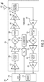
- FIG. 3 depicts an apparatus for filtering out near end blocking signals and transmit leakage.
- the apparatus, 300 includes biquad filter stages as described below.
- An auxiliary path is added in parallel with the main path biquad filter stage. This auxiliary path carries half the current from the mixer output.
- a receive signal is received at antenna 302 and sent to low noise amplifier (LNA) 304.
- LNA 304 is coupled to RF transformer 306, shown here as an air core transformer.
- RF transformer 306 is connected to mixer 308.
- the mixer output is sent to an RC filter, consisting of transmit resistor 310 and transmit capacitor 312.
- the RC filter provides initial filtering of the received signal.
- the output from the RC filter is sent to two paths of the biquad filter, a main path and an auxiliary path.
- the main path is sent to the first stage of the biquad filter assembly, to RT resistor 314 and capacitor C1 316.
- the main path leads from the RC filter to the input of the main path biquad filter operational transconductance amplifier (OTA) 318.
- OTA operational transconductance amplifier
- a two stage negative feedback loop is formed with RT 314, C1 316 and RT resistor 320.
- RT resistor 320 is provided on the input of offset amplifier 322.
- Offset amplifier 322 acts as an active attenuator as part of the two stage negative feedback look.
- the first stage of the biquad filter provides for the partially filtered signal to be provided to the negative input of the second stage OTA2 328.
- the negative path input to OTA 328 also includes capacitor C2 324.
- OTA2 328 also receives input on the negative input pin from the auxiliary path.
- the auxiliary path begins after transmit resistor 310 and begins with an input to the negative pin of OTA3 334 also obtains input on the negative pin from resistor R 330 and capacitor C332.
- the input from OTA3 334 is also provided as input to OTA2 328, but passes through line resistor 336.
- Each OTA is typically comprised of two stages, with the second stage acting as the driving stage.
- the second stage is also used for combining the main path and auxiliary paths.
- the first stage of the OTA typically consumes less than 1MA of current.
- the second stage of the OTA may be a class AB amplifier, which consumes some current in the absence of a signal.
- the RC filter jamming alone is not capable of providing the required level of rejection where weak receive signals are found.
- the first stage of the LNA 304 cannot provide filtering with only one pole and would be saturated in situations where high transmit leakage occurs in conjunction with weak signal reception.
- the output from the biquad filter provides sufficient filtering if the first stage of the biquad filter can tolerate the blocking transmit signals. In such cases, the second stage of biquad filtering is not needed.
- the first stage of the biquad filter is saturated and the second stage provided as embodiments herein, is needed to suppress the jamming transmit signals and allow recovery of the weaker desired receive signal.
- the swing of the input signal level at OTA1 318 and OTA3 334 is half (-6dB) of the swing provided by conventional architecture, while gain remains the same as in conventional architecture. This reduction enables more efficient filtering with fewer additional components.
- the number of auxiliary paths is not limited, and it may be desirable to add additional paths that may be disabled when not in use. Adding additional auxiliary paths may also provide addition reduction and margin for swing.
- the number of additional paths that may be added is limited by the gross bandwidth of the OTA, which may limit the improvement from additional auxiliary paths. The reason for less improvement from successive auxiliary paths is that each added auxiliary path contributes additional noise to the base band output, which in the case of high gain, could be negligible.
- the auxiliary path depicted in FIGs. 3 and 4 provides another path for the desired signal and operates to reduce the swing requirement at the main path output by 6dB, in some cases. In other transmit situations the swing path output may be reduced by a different amount.
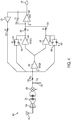
- FIG. 4 illustrates a further embodiment which allows for the first stage of the OTA to be shared by both the main and auxiliary paths.
- Each OTA has two stages. In the embodiment described below, stage one is shared between the main and auxiliary paths.
- the assembly, 400 also includes antenna 302 for receiving signals.
- Initial signal reception is the same as described for FIG. 3 , with the received signal passing through LNA 304 and RF transformer 306, and mixer 308.
- Initial stage RC filtering is provided by RTx 310 and CTx 312.
- the signal is passed to RT 320 and -1 offset amplifier 322; RT 412 and C1 414; and also to OTA stage 1 402. From OTA 402 the signal path is split between two stage 2 OTAs, 404 and 406.
- the main path continues with the output from OTA 404 passing through lines resistor 326 and on to OTA2 328 and C2 324.
- the split path is routed to OTA 406.
- the output of OTA 406 is combined with the output from C 408 and R 410 before passing through lines resistor 336.
- the auxiliary path is provided as input to OTA2 328.
- the output of OTA2 328 is provided as output 338.
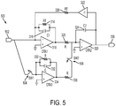
- FIG. 5 illustrates a further embodiment with switches provided to disable the auxiliary path.
- Switch 1 receives input 502 and allows for a portion of the received signal to be diverted into the auxiliary path.
- Switch 2 (SW2) 506 provides the output of OTA3 334 to be provided as input to OTA2 328.
- SW1 504 and SW2506 are open, the auxiliary path is disabled and has no effect on the main biquad filtering path.
- Both SW1 502 and SW2 504 are connected to the virtual ground nodes of OTA1 318 and OTA 2 326.
- FIG. 6 illustrates the simulation results of embodiments described above.
- the results show the improvements from the use of the auxiliary path.
- the improved filtering results from the base band first stage not being saturated, as the auxiliary path to the base band filtering is immediately after the mixer, resulting in improved filtering.
- FIG. 7 is a flowchart of the steps of minimizing transmit signal interference of a weaker received signal using the apparatus described above.
- the method, 700 begins with receiving a signal at step 702.
- the weaker received signal is then amplified in a low noise amplifier in step 704.
- An RC filter provides initial filtering of the received signal in step 708.
- the RC filtered signal is then divided by a predetermined number in step 708. This predetermined number may correspond to the number of main and auxiliary biquad filter paths being utilized. In the event that the first OTA is shared, dividing of the RC filtered signal may occur after the first stage of biquad filtering.
- step 710 the first portion of the RC filtered signal is routed to a main path of the biquad filter.
- the second portion of the RC filtered signal is routed to an auxiliary path of the biquad filter in step 712.
- steps 714 Once both or all of the divided signal portions have been routed through the first stage of the biquad filter, they are recombined in step 714.
- the recombined signal is then passed to the second stage of the biquad filter for additional filtering in step 716.
- FIG.8 provides a flowchart of the steps of a method using an auxiliary path that may be switched on or off as needed.
- the method, 800 begins with the receiving of a signal at step 802. The signal is then amplified in step 804. In step 806, an RC filter provides first filtering of the signal. In step 808, a determination of whether to use an auxiliary path for additional biquad filtering is made. If the decision is made not to use the auxiliary path, the signal is routed to the main path of the biquad filter in step 810. If the determination indicates that the auxiliary path is to be used, the signal is divided by a predetermined path in step 812.
- the number of auxiliary paths is not limited, and more may be used than are depicted, however, the scope of the disclosure provides for the use of more auxiliary paths than are depicted.
- the first stage of the biquad filter, the OTA may be shared, with the division of the signal into main and auxiliary paths occurring after the first stage of the biquad filter.
- auxiliary path switches along the auxiliary path are opened in step 814, to route the signal through the auxiliary path and into the second stage of the biquad filter.
- a first portion of the divided signal is routed to the main path of the biquad filter.
- a second portion of the divided signal is routed to the auxiliary path of the biquad filter.
- the first and second portions of the divided signal are recombined at step 820.
- the recombined signal is then filtered in the second stage of the biquad filter in step 822.
- the auxiliary path determination may be performed by a processor, which may also direct the setting of the switches.
- a processor which may also direct the setting of the switches.
- the disclosure provides that the paths may be reconfigured to provide the desired number of auxiliary paths by a processor.
- DSP Digital Signal Processor
- ASIC Application Specific Integrated Circuit
- FPGA Field Programmable Gate Array
- a general purpose processor may be a microprocessor, but in the alternative, the processor may be any conventional processor, controller, microcontroller, or state machine.
- a processor may also be implemented as a combination of computing devices, e.g., a combination of a DSP and a microprocessor, a plurality of microprocessors, one or more microprocessors in conjunction with a DSP core, or any other such configuration.
- the functions described may be implemented in hardware, software, firmware, or any combination thereof. If implemented in software, the functions may be stored on or transmitter over as one or more instructions or code on a computer-readable medium.
- Computer-readable media includes both computer storage media and communication media including any medium that facilitates transfer of a computer program from one place to another.
- a storage media may be any available media that can be accessed by a computer.
- such computer-readable media can comprise RAM, ROM EEPROM, CD-ROM or other optical disk storage or other magnetic storage devices, or any other medium that can be used to carry or store desired program code in the form of instructions or data structures and that can be accessed by a computer.
- any connection is properly termed a computer-readable medium.
- Disk and disc includes compact disc (CD), laser disc, optical disc, digital versatile disc (DVD), floppy disk and blu-ray disc where disks usually reproduce data magnetically, while discs reproduce data optically with lasers. Combinations of the above should also be included within the scope of computer-readable media.
Landscapes
- Engineering & Computer Science (AREA)
- Computer Networks & Wireless Communication (AREA)
- Signal Processing (AREA)
- Noise Elimination (AREA)
- Physics & Mathematics (AREA)
- Computer Hardware Design (AREA)
- Mathematical Physics (AREA)
- Networks Using Active Elements (AREA)
- Transceivers (AREA)
Claims (13)
- Ein Verfahren (700) zum Minimieren von Sendesignalinterferenz, das Folgendes aufweist:Empfangen (702) eines Signals;Verstärken (704) des empfangenen Signals;Mischen des empfangenen Signals mit einem Zwischenfrequenzsignal zum Erlangen eines modulierten Basisbandsignals;Filtern (706) des modulierten Basisbandsignals in einem ersten Filter;Aufteilen (708) des ersten gefilterten modulierten Basisbandsignals auf einen Haupt-Biquad-Filterpfad und wenigstens einen Hilfs-Biquad-Filterpfad;Senden (710) eines ersten aufgeteilten Teils des modulierten Basisbandsignals an den Hauptpfad eines Biquad-Filters, was ein erstes biquad-gefiltertes Signal erzeugt;Senden (712) eines zweiten aufgeteilten Teils des modulierten Basisbandsignals an den Hilfspfad des Biquad-Filters, was ein zweites biquad-gefiltertes Signal erzeugt;Rekombinieren (714) des ersten biquad-gefilterten Signals mit dem zweiten biquad-gefilterten Signal vor einer zweiten Stufe des Biquad-Filters; undFiltern (716) des rekombinierten biquad-gefilterten Signals in der zweiten Stufe des Biquad-Filters.
- Verfahren (700) nach Anspruch 1, wobei das erste gefilterte modulierte Basisbandsignal auf den Haupt-Biquad-Filterpfad und mehrere Hilfs-Biquad-Filterpfade aufgeteilt wird.
- Verfahren (700) nach Anspruch 1, wobei der Hilfs-Biquad-Filterpfad ein paralleler Pfad ist.
- Verfahren (700) nach Anspruch 2, wobei die mehreren Hilfs-Biquad-Filterpfade parallel zueinander sind.
- Verfahren (700) nach Anspruch 1, wobei die mehreren Hilfs-Biquad-Filterpfade parallel zueinander sind.
- Verfahren (700) nach Anspruch 1, wobei vor dem Weiterleiten des ersten gefilterten modulierten Basisbandsignals eine Bestimmung (808) hinsichtlich einer Nutzung eines Hilfspfades vorgenommen wird.
- Verfahren (700) nach Anspruch 1, das weiter Bestimmen (808) aufweist, ob mehrere Hilfspfade verwendet werden sollen.
- Eine Vorrichtung (300) zum Minimieren von Sendesignalinterferenz, die Folgendes aufweist:Mittel (302) zum Empfangen eines Signals;Mittel (304) zum Verstärken des empfangenen Signals;Mittel (308) zum Mischen des empfangenen Signals mit einem Zwischenfrequenzsignal zum Erlangen eines modulierten Basisbandsignals;Mittel (310, 312) zum Filtern des modulierten Basisbandsignals in einem ersten Filter;Mittel zum Aufteilen des ersten gefilterten modulierten Basisbandsignals auf einen Haupt-Biquad-Filterpfad und wenigstens einen Hilfs-Biquad-Filterpfad;Mittel zum Senden eines ersten aufgeteilten Teils des modulierten Basisbandsignals an den Hauptpfad eines Biquad-Filters, was ein erstes biquad-gefiltertes Signal erzeugt;Mittel zum Senden eines zweiten aufgeteilten Teils des modulierten Basisbandsignals an den Hilfspfad des Biquad-Filters, was ein zweites biquad-gefiltertes Signal erzeugt;Mittel zum Rekombinieren des ersten biquad-gefilterten Signals mit dem zweiten biquad-gefilterten Signal vor einer zweiten Stufe des Biquad-Filters; undMittel zum Filtern des rekombinierten biquad-gefilterten Signals in der zweiten Stufe des Biquad-Filters.
- Vorrichtung (300) nach Anspruch 8, die weiter Mittel aufweist zum Aufteilen des ersten gefilterten modulierten Basisbandsignals auf den Haupt-Biquad-Filterpfad und mehrere Hilfs-Biquad-Filterpfade.
- Vorrichtung (300) nach Anspruch 8, wobei die Mittel zum Aufteilen des ersten gefilterten modulierten Basisbandsignals den Hilfs-Biquad-Filterpfad an einen parallelen Pfad weiterleiten.
- Vorrichtung (300) nach Anspruch 8, wobei die Mittel zum Aufteilen das aufgeteilte Signal an mehrere paralelle Hilfs-Biquad-Filterpfade weiterleiten.
- Vorrichtung (300) nach Anspruch 8, wobei die Mittel zum Filtern eine erste Stufe eines Biquad-Filters gemeinsam für einen Haupt-Biquad-Filterpfad und einen Hilfs-Biquad-Filterpfad verwenden.
- Ein nicht transitorisches computerlesbares Medium, das Programminstruktionen beinhaltet, die, wenn sie durch einen Prozessor ausgeführt werden, den Prozessor veranlassen zum Durchführen des Verfahrens nach einem der Ansprüche 1 bis 7.
Applications Claiming Priority (2)
| Application Number | Priority Date | Filing Date | Title |
|---|---|---|---|
| US14/331,685 US9647638B2 (en) | 2014-07-15 | 2014-07-15 | Architecture to reject near end blockers and transmit leakage |
| PCT/US2015/036267 WO2016010669A1 (en) | 2014-07-15 | 2015-06-17 | Architecture to reject near end blockers and transmit leakage |
Publications (2)
| Publication Number | Publication Date |
|---|---|
| EP3170263A1 EP3170263A1 (de) | 2017-05-24 |
| EP3170263B1 true EP3170263B1 (de) | 2018-01-10 |
Family
ID=53682784
Family Applications (1)
| Application Number | Title | Priority Date | Filing Date |
|---|---|---|---|
| EP15739371.1A Not-in-force EP3170263B1 (de) | 2014-07-15 | 2015-06-17 | Architektur zur abweisung von nahendblockern und übertragungslecks |
Country Status (5)
| Country | Link |
|---|---|
| US (1) | US9647638B2 (de) |
| EP (1) | EP3170263B1 (de) |
| JP (1) | JP2017525285A (de) |
| CN (1) | CN106537774A (de) |
| WO (1) | WO2016010669A1 (de) |
Families Citing this family (3)
| Publication number | Priority date | Publication date | Assignee | Title |
|---|---|---|---|---|
| US10200067B1 (en) | 2017-09-29 | 2019-02-05 | Apple Inc. | Radio frequency transceiver front-end systems and methods |
| CN108540106B (zh) * | 2018-03-30 | 2022-02-01 | 东南大学 | 一种电流模射频带通滤波器 |
| CN112751548B (zh) * | 2019-10-31 | 2024-06-18 | 瑞昱半导体股份有限公司 | 滤波器以及运行方法 |
Family Cites Families (19)
| Publication number | Priority date | Publication date | Assignee | Title |
|---|---|---|---|---|
| JPH05284182A (ja) * | 1992-04-02 | 1993-10-29 | Yamatake Honeywell Co Ltd | 受信フィルタ回路 |
| HK1040467B (zh) * | 1998-07-24 | 2005-03-04 | 环球通讯科技半导体公司 | 通信系統,單芯片rf通信系統及rf通信系統的控制方法 |
| US6188281B1 (en) | 1998-09-30 | 2001-02-13 | Maxim Integrated Products, Inc. | Linear transconductance circuits having class AB amplifiers parallel coupled with concave compensation circuits |
| US6184748B1 (en) | 1998-09-30 | 2001-02-06 | Lsi Logic Corporation | Magnitude and group delay shaping circuit in continuous-time read channel filters |
| US7555263B1 (en) * | 1999-10-21 | 2009-06-30 | Broadcom Corporation | Adaptive radio transceiver |
| CN100433542C (zh) * | 2002-06-05 | 2008-11-12 | Rf信息公司 | 用于处理电视信号的电路、接收机及方法 |
| WO2005060095A1 (en) * | 2003-12-12 | 2005-06-30 | Dsp Group Inc. | Complex filter with higher order pole |
| JP2005328260A (ja) | 2004-05-13 | 2005-11-24 | Mitsubishi Electric Corp | バンドパスフィルタ |
| US8243864B2 (en) * | 2004-11-19 | 2012-08-14 | Qualcomm, Incorporated | Noise reduction filtering in a wireless communication system |
| US8036623B2 (en) * | 2007-03-13 | 2011-10-11 | Qualcomm, Incorporated | Wireless receiver with notch filter to reduce effects of transmit signal leakage |
| US8706055B2 (en) * | 2007-03-23 | 2014-04-22 | Qualcomm Incorporated | Reduction of second-order distortion caused by transmit signal leakage |
| KR101324197B1 (ko) * | 2007-09-17 | 2013-11-06 | 삼성전자주식회사 | 이퀄라이저 용 필터 |
| US7619472B1 (en) * | 2008-06-04 | 2009-11-17 | Newport Media, Inc. | Noise-shaped blocker-reject amplifier |
| US8594603B2 (en) * | 2009-11-08 | 2013-11-26 | The Trustees Of Columbia University In The City Of New York | Systems and methods for cancelling interferers in a receiver |
| US7986187B1 (en) | 2010-03-04 | 2011-07-26 | Bose Corporation | Versatile audio power amplifier |
| WO2011117911A1 (ja) | 2010-03-23 | 2011-09-29 | 富士通株式会社 | 周波数可変フィルタ |
| JP5665571B2 (ja) | 2011-01-28 | 2015-02-04 | ルネサスエレクトロニクス株式会社 | 半導体集積回路およびその動作方法 |
| GB2500067A (en) | 2012-03-09 | 2013-09-11 | Renesas Mobile Corp | An N-path filter for notching out unwanted signals in wireless receivers |
| KR20150053784A (ko) * | 2012-09-05 | 2015-05-18 | 뉴랜스, 인코포레이티드. | 바이쿼드 캘리브레이션 |
-
2014
- 2014-07-15 US US14/331,685 patent/US9647638B2/en active Active
-
2015
- 2015-06-17 EP EP15739371.1A patent/EP3170263B1/de not_active Not-in-force
- 2015-06-17 CN CN201580037560.7A patent/CN106537774A/zh active Pending
- 2015-06-17 JP JP2017502094A patent/JP2017525285A/ja active Pending
- 2015-06-17 WO PCT/US2015/036267 patent/WO2016010669A1/en not_active Ceased
Also Published As
| Publication number | Publication date |
|---|---|
| EP3170263A1 (de) | 2017-05-24 |
| CN106537774A (zh) | 2017-03-22 |
| WO2016010669A1 (en) | 2016-01-21 |
| JP2017525285A (ja) | 2017-08-31 |
| US9647638B2 (en) | 2017-05-09 |
| US20160020752A1 (en) | 2016-01-21 |
Similar Documents
| Publication | Publication Date | Title |
|---|---|---|
| US9692470B2 (en) | Low noise amplifier and notch filter | |
| KR20180039059A (ko) | 복수의 lna들 간의 캐스캐이딩된 스위치 | |
| AU2018435590B2 (en) | Sidelink channel configuration method, terminal device, and network device | |
| US9800280B2 (en) | Noise suppression in radio frequency receivers | |
| CN110463050A (zh) | 多频带射频接收 | |
| JP4894503B2 (ja) | 無線通信装置 | |
| EP3170263B1 (de) | Architektur zur abweisung von nahendblockern und übertragungslecks | |
| EP3068054B1 (de) | Unterstützung von multifrequenzbändern | |
| US10547289B2 (en) | High order miller N-path filter | |
| CN110915142B (zh) | 具有用于不连续载波聚合的复基带滤波器的滤波器电路 | |
| KR20240060795A (ko) | 구성 가능한 경로를 갖는 팬아웃 멀티-스테이지 증폭기 | |
| CN120883581A (zh) | 用于调整数模转换器输出功率的波峰因子降低 | |
| US10742302B2 (en) | Wireless communication device transceiving signals by using carrier aggregation in multi input multi output system | |
| US8451046B2 (en) | System and method for switch leakage cancellation | |
| US12003267B2 (en) | High linearity modes in wireless receivers | |
| US11569865B1 (en) | Reconfigurable baseband filter | |
| CN113169753B (zh) | 收发开关 | |
| US9425755B1 (en) | Swing limiter circuit | |
| EP2693648A1 (de) | Mobile drahtlose Kommunikationsvorrichtung mit HF-LTE-Schaltern und zugehörige Verfahren | |
| WO2020103450A1 (en) | Programmable on-chip self-calibrating balanced attenuator | |
| WO2025159853A1 (en) | Transmitter architecture suppressing harmonic signals between transmitters using a filter and a reconfigurable power amplifier | |
| HK1182572B (en) | Dual association local area network transceiver and methods for use therewith | |
| HK1182572A1 (zh) | 雙相關的局域網收發器及其使用方法 |
Legal Events
| Date | Code | Title | Description |
|---|---|---|---|
| PUAI | Public reference made under article 153(3) epc to a published international application that has entered the european phase |
Free format text: ORIGINAL CODE: 0009012 |
|
| 17P | Request for examination filed |
Effective date: 20170208 |
|
| AK | Designated contracting states |
Kind code of ref document: A1 Designated state(s): AL AT BE BG CH CY CZ DE DK EE ES FI FR GB GR HR HU IE IS IT LI LT LU LV MC MK MT NL NO PL PT RO RS SE SI SK SM TR |
|
| AX | Request for extension of the european patent |
Extension state: BA ME |
|
| GRAP | Despatch of communication of intention to grant a patent |
Free format text: ORIGINAL CODE: EPIDOSNIGR1 |
|
| DAV | Request for validation of the european patent (deleted) | ||
| DAX | Request for extension of the european patent (deleted) | ||
| INTG | Intention to grant announced |
Effective date: 20170725 |
|
| GRAS | Grant fee paid |
Free format text: ORIGINAL CODE: EPIDOSNIGR3 |
|
| GRAA | (expected) grant |
Free format text: ORIGINAL CODE: 0009210 |
|
| AK | Designated contracting states |
Kind code of ref document: B1 Designated state(s): AL AT BE BG CH CY CZ DE DK EE ES FI FR GB GR HR HU IE IS IT LI LT LU LV MC MK MT NL NO PL PT RO RS SE SI SK SM TR |
|
| REG | Reference to a national code |
Ref country code: FR Ref legal event code: PLFP Year of fee payment: 4 |
|
| REG | Reference to a national code |
Ref country code: CH Ref legal event code: EP Ref country code: AT Ref legal event code: REF Ref document number: 963496 Country of ref document: AT Kind code of ref document: T Effective date: 20180115 |
|
| REG | Reference to a national code |
Ref country code: IE Ref legal event code: FG4D |
|
| REG | Reference to a national code |
Ref country code: DE Ref legal event code: R096 Ref document number: 602015007486 Country of ref document: DE |
|
| REG | Reference to a national code |
Ref country code: NL Ref legal event code: MP Effective date: 20180110 |
|
| PGFP | Annual fee paid to national office [announced via postgrant information from national office to epo] |
Ref country code: FR Payment date: 20180112 Year of fee payment: 4 |
|
| REG | Reference to a national code |
Ref country code: AT Ref legal event code: MK05 Ref document number: 963496 Country of ref document: AT Kind code of ref document: T Effective date: 20180110 |
|
| PG25 | Lapsed in a contracting state [announced via postgrant information from national office to epo] |
Ref country code: NL Free format text: LAPSE BECAUSE OF FAILURE TO SUBMIT A TRANSLATION OF THE DESCRIPTION OR TO PAY THE FEE WITHIN THE PRESCRIBED TIME-LIMIT Effective date: 20180110 |
|
| PG25 | Lapsed in a contracting state [announced via postgrant information from national office to epo] |
Ref country code: ES Free format text: LAPSE BECAUSE OF FAILURE TO SUBMIT A TRANSLATION OF THE DESCRIPTION OR TO PAY THE FEE WITHIN THE PRESCRIBED TIME-LIMIT Effective date: 20180110 Ref country code: HR Free format text: LAPSE BECAUSE OF FAILURE TO SUBMIT A TRANSLATION OF THE DESCRIPTION OR TO PAY THE FEE WITHIN THE PRESCRIBED TIME-LIMIT Effective date: 20180110 Ref country code: LT Free format text: LAPSE BECAUSE OF FAILURE TO SUBMIT A TRANSLATION OF THE DESCRIPTION OR TO PAY THE FEE WITHIN THE PRESCRIBED TIME-LIMIT Effective date: 20180110 Ref country code: CY Free format text: LAPSE BECAUSE OF FAILURE TO SUBMIT A TRANSLATION OF THE DESCRIPTION OR TO PAY THE FEE WITHIN THE PRESCRIBED TIME-LIMIT Effective date: 20180110 Ref country code: FI Free format text: LAPSE BECAUSE OF FAILURE TO SUBMIT A TRANSLATION OF THE DESCRIPTION OR TO PAY THE FEE WITHIN THE PRESCRIBED TIME-LIMIT Effective date: 20180110 Ref country code: NO Free format text: LAPSE BECAUSE OF FAILURE TO SUBMIT A TRANSLATION OF THE DESCRIPTION OR TO PAY THE FEE WITHIN THE PRESCRIBED TIME-LIMIT Effective date: 20180410 |
|
| PGFP | Annual fee paid to national office [announced via postgrant information from national office to epo] |
Ref country code: DE Payment date: 20180102 Year of fee payment: 4 |
|
| PG25 | Lapsed in a contracting state [announced via postgrant information from national office to epo] |
Ref country code: IS Free format text: LAPSE BECAUSE OF FAILURE TO SUBMIT A TRANSLATION OF THE DESCRIPTION OR TO PAY THE FEE WITHIN THE PRESCRIBED TIME-LIMIT Effective date: 20180510 Ref country code: GR Free format text: LAPSE BECAUSE OF FAILURE TO SUBMIT A TRANSLATION OF THE DESCRIPTION OR TO PAY THE FEE WITHIN THE PRESCRIBED TIME-LIMIT Effective date: 20180411 Ref country code: PL Free format text: LAPSE BECAUSE OF FAILURE TO SUBMIT A TRANSLATION OF THE DESCRIPTION OR TO PAY THE FEE WITHIN THE PRESCRIBED TIME-LIMIT Effective date: 20180110 Ref country code: RS Free format text: LAPSE BECAUSE OF FAILURE TO SUBMIT A TRANSLATION OF THE DESCRIPTION OR TO PAY THE FEE WITHIN THE PRESCRIBED TIME-LIMIT Effective date: 20180110 Ref country code: SE Free format text: LAPSE BECAUSE OF FAILURE TO SUBMIT A TRANSLATION OF THE DESCRIPTION OR TO PAY THE FEE WITHIN THE PRESCRIBED TIME-LIMIT Effective date: 20180110 Ref country code: LV Free format text: LAPSE BECAUSE OF FAILURE TO SUBMIT A TRANSLATION OF THE DESCRIPTION OR TO PAY THE FEE WITHIN THE PRESCRIBED TIME-LIMIT Effective date: 20180110 Ref country code: BG Free format text: LAPSE BECAUSE OF FAILURE TO SUBMIT A TRANSLATION OF THE DESCRIPTION OR TO PAY THE FEE WITHIN THE PRESCRIBED TIME-LIMIT Effective date: 20180410 Ref country code: AT Free format text: LAPSE BECAUSE OF FAILURE TO SUBMIT A TRANSLATION OF THE DESCRIPTION OR TO PAY THE FEE WITHIN THE PRESCRIBED TIME-LIMIT Effective date: 20180110 |
|
| REG | Reference to a national code |
Ref country code: DE Ref legal event code: R097 Ref document number: 602015007486 Country of ref document: DE |
|
| PG25 | Lapsed in a contracting state [announced via postgrant information from national office to epo] |
Ref country code: IT Free format text: LAPSE BECAUSE OF FAILURE TO SUBMIT A TRANSLATION OF THE DESCRIPTION OR TO PAY THE FEE WITHIN THE PRESCRIBED TIME-LIMIT Effective date: 20180110 Ref country code: AL Free format text: LAPSE BECAUSE OF FAILURE TO SUBMIT A TRANSLATION OF THE DESCRIPTION OR TO PAY THE FEE WITHIN THE PRESCRIBED TIME-LIMIT Effective date: 20180110 Ref country code: EE Free format text: LAPSE BECAUSE OF FAILURE TO SUBMIT A TRANSLATION OF THE DESCRIPTION OR TO PAY THE FEE WITHIN THE PRESCRIBED TIME-LIMIT Effective date: 20180110 |
|
| PLBE | No opposition filed within time limit |
Free format text: ORIGINAL CODE: 0009261 |
|
| STAA | Information on the status of an ep patent application or granted ep patent |
Free format text: STATUS: NO OPPOSITION FILED WITHIN TIME LIMIT |
|
| PG25 | Lapsed in a contracting state [announced via postgrant information from national office to epo] |
Ref country code: DK Free format text: LAPSE BECAUSE OF FAILURE TO SUBMIT A TRANSLATION OF THE DESCRIPTION OR TO PAY THE FEE WITHIN THE PRESCRIBED TIME-LIMIT Effective date: 20180110 Ref country code: CZ Free format text: LAPSE BECAUSE OF FAILURE TO SUBMIT A TRANSLATION OF THE DESCRIPTION OR TO PAY THE FEE WITHIN THE PRESCRIBED TIME-LIMIT Effective date: 20180110 Ref country code: SK Free format text: LAPSE BECAUSE OF FAILURE TO SUBMIT A TRANSLATION OF THE DESCRIPTION OR TO PAY THE FEE WITHIN THE PRESCRIBED TIME-LIMIT Effective date: 20180110 Ref country code: SM Free format text: LAPSE BECAUSE OF FAILURE TO SUBMIT A TRANSLATION OF THE DESCRIPTION OR TO PAY THE FEE WITHIN THE PRESCRIBED TIME-LIMIT Effective date: 20180110 |
|
| 26N | No opposition filed |
Effective date: 20181011 |
|
| REG | Reference to a national code |
Ref country code: CH Ref legal event code: PL |
|
| REG | Reference to a national code |
Ref country code: BE Ref legal event code: MM Effective date: 20180630 |
|
| REG | Reference to a national code |
Ref country code: IE Ref legal event code: MM4A |
|
| PG25 | Lapsed in a contracting state [announced via postgrant information from national office to epo] |
Ref country code: LU Free format text: LAPSE BECAUSE OF NON-PAYMENT OF DUE FEES Effective date: 20180617 Ref country code: MC Free format text: LAPSE BECAUSE OF FAILURE TO SUBMIT A TRANSLATION OF THE DESCRIPTION OR TO PAY THE FEE WITHIN THE PRESCRIBED TIME-LIMIT Effective date: 20180110 |
|
| PG25 | Lapsed in a contracting state [announced via postgrant information from national office to epo] |
Ref country code: CH Free format text: LAPSE BECAUSE OF NON-PAYMENT OF DUE FEES Effective date: 20180630 Ref country code: LI Free format text: LAPSE BECAUSE OF NON-PAYMENT OF DUE FEES Effective date: 20180630 Ref country code: IE Free format text: LAPSE BECAUSE OF NON-PAYMENT OF DUE FEES Effective date: 20180617 |
|
| PG25 | Lapsed in a contracting state [announced via postgrant information from national office to epo] |
Ref country code: BE Free format text: LAPSE BECAUSE OF NON-PAYMENT OF DUE FEES Effective date: 20180630 |
|
| REG | Reference to a national code |
Ref country code: DE Ref legal event code: R119 Ref document number: 602015007486 Country of ref document: DE |
|
| PG25 | Lapsed in a contracting state [announced via postgrant information from national office to epo] |
Ref country code: MT Free format text: LAPSE BECAUSE OF NON-PAYMENT OF DUE FEES Effective date: 20180617 |
|
| GBPC | Gb: european patent ceased through non-payment of renewal fee |
Effective date: 20190617 |
|
| PG25 | Lapsed in a contracting state [announced via postgrant information from national office to epo] |
Ref country code: TR Free format text: LAPSE BECAUSE OF FAILURE TO SUBMIT A TRANSLATION OF THE DESCRIPTION OR TO PAY THE FEE WITHIN THE PRESCRIBED TIME-LIMIT Effective date: 20180110 |
|
| PG25 | Lapsed in a contracting state [announced via postgrant information from national office to epo] |
Ref country code: DE Free format text: LAPSE BECAUSE OF NON-PAYMENT OF DUE FEES Effective date: 20200101 Ref country code: GB Free format text: LAPSE BECAUSE OF NON-PAYMENT OF DUE FEES Effective date: 20190617 |
|
| PG25 | Lapsed in a contracting state [announced via postgrant information from national office to epo] |
Ref country code: PT Free format text: LAPSE BECAUSE OF FAILURE TO SUBMIT A TRANSLATION OF THE DESCRIPTION OR TO PAY THE FEE WITHIN THE PRESCRIBED TIME-LIMIT Effective date: 20180110 |
|
| PG25 | Lapsed in a contracting state [announced via postgrant information from national office to epo] |
Ref country code: RO Free format text: LAPSE BECAUSE OF FAILURE TO SUBMIT A TRANSLATION OF THE DESCRIPTION OR TO PAY THE FEE WITHIN THE PRESCRIBED TIME-LIMIT Effective date: 20180110 Ref country code: MK Free format text: LAPSE BECAUSE OF NON-PAYMENT OF DUE FEES Effective date: 20180110 Ref country code: FR Free format text: LAPSE BECAUSE OF NON-PAYMENT OF DUE FEES Effective date: 20190630 Ref country code: HU Free format text: LAPSE BECAUSE OF FAILURE TO SUBMIT A TRANSLATION OF THE DESCRIPTION OR TO PAY THE FEE WITHIN THE PRESCRIBED TIME-LIMIT; INVALID AB INITIO Effective date: 20150617 |
|
| PG25 | Lapsed in a contracting state [announced via postgrant information from national office to epo] |
Ref country code: SI Free format text: LAPSE BECAUSE OF NON-PAYMENT OF DUE FEES Effective date: 20180617 |