EP3163564A1 - Organic light emitting diode display device - Google Patents
Organic light emitting diode display device Download PDFInfo
- Publication number
- EP3163564A1 EP3163564A1 EP16196473.9A EP16196473A EP3163564A1 EP 3163564 A1 EP3163564 A1 EP 3163564A1 EP 16196473 A EP16196473 A EP 16196473A EP 3163564 A1 EP3163564 A1 EP 3163564A1
- Authority
- EP
- European Patent Office
- Prior art keywords
- vertical synchronization
- data
- display device
- module
- period
- Prior art date
- Legal status (The legal status is an assumption and is not a legal conclusion. Google has not performed a legal analysis and makes no representation as to the accuracy of the status listed.)
- Granted
Links
Images



Classifications
-
- G—PHYSICS
- G09—EDUCATION; CRYPTOGRAPHY; DISPLAY; ADVERTISING; SEALS
- G09G—ARRANGEMENTS OR CIRCUITS FOR CONTROL OF INDICATING DEVICES USING STATIC MEANS TO PRESENT VARIABLE INFORMATION
- G09G3/00—Control arrangements or circuits, of interest only in connection with visual indicators other than cathode-ray tubes
- G09G3/20—Control arrangements or circuits, of interest only in connection with visual indicators other than cathode-ray tubes for presentation of an assembly of a number of characters, e.g. a page, by composing the assembly by combination of individual elements arranged in a matrix no fixed position being assigned to or needed to be assigned to the individual characters or partial characters
- G09G3/22—Control arrangements or circuits, of interest only in connection with visual indicators other than cathode-ray tubes for presentation of an assembly of a number of characters, e.g. a page, by composing the assembly by combination of individual elements arranged in a matrix no fixed position being assigned to or needed to be assigned to the individual characters or partial characters using controlled light sources
- G09G3/30—Control arrangements or circuits, of interest only in connection with visual indicators other than cathode-ray tubes for presentation of an assembly of a number of characters, e.g. a page, by composing the assembly by combination of individual elements arranged in a matrix no fixed position being assigned to or needed to be assigned to the individual characters or partial characters using controlled light sources using electroluminescent panels
- G09G3/32—Control arrangements or circuits, of interest only in connection with visual indicators other than cathode-ray tubes for presentation of an assembly of a number of characters, e.g. a page, by composing the assembly by combination of individual elements arranged in a matrix no fixed position being assigned to or needed to be assigned to the individual characters or partial characters using controlled light sources using electroluminescent panels semiconductive, e.g. using light-emitting diodes [LED]
- G09G3/3208—Control arrangements or circuits, of interest only in connection with visual indicators other than cathode-ray tubes for presentation of an assembly of a number of characters, e.g. a page, by composing the assembly by combination of individual elements arranged in a matrix no fixed position being assigned to or needed to be assigned to the individual characters or partial characters using controlled light sources using electroluminescent panels semiconductive, e.g. using light-emitting diodes [LED] organic, e.g. using organic light-emitting diodes [OLED]
-
- G—PHYSICS
- G09—EDUCATION; CRYPTOGRAPHY; DISPLAY; ADVERTISING; SEALS
- G09G—ARRANGEMENTS OR CIRCUITS FOR CONTROL OF INDICATING DEVICES USING STATIC MEANS TO PRESENT VARIABLE INFORMATION
- G09G3/00—Control arrangements or circuits, of interest only in connection with visual indicators other than cathode-ray tubes
- G09G3/20—Control arrangements or circuits, of interest only in connection with visual indicators other than cathode-ray tubes for presentation of an assembly of a number of characters, e.g. a page, by composing the assembly by combination of individual elements arranged in a matrix no fixed position being assigned to or needed to be assigned to the individual characters or partial characters
- G09G3/22—Control arrangements or circuits, of interest only in connection with visual indicators other than cathode-ray tubes for presentation of an assembly of a number of characters, e.g. a page, by composing the assembly by combination of individual elements arranged in a matrix no fixed position being assigned to or needed to be assigned to the individual characters or partial characters using controlled light sources
- G09G3/30—Control arrangements or circuits, of interest only in connection with visual indicators other than cathode-ray tubes for presentation of an assembly of a number of characters, e.g. a page, by composing the assembly by combination of individual elements arranged in a matrix no fixed position being assigned to or needed to be assigned to the individual characters or partial characters using controlled light sources using electroluminescent panels
- G09G3/32—Control arrangements or circuits, of interest only in connection with visual indicators other than cathode-ray tubes for presentation of an assembly of a number of characters, e.g. a page, by composing the assembly by combination of individual elements arranged in a matrix no fixed position being assigned to or needed to be assigned to the individual characters or partial characters using controlled light sources using electroluminescent panels semiconductive, e.g. using light-emitting diodes [LED]
- G09G3/3208—Control arrangements or circuits, of interest only in connection with visual indicators other than cathode-ray tubes for presentation of an assembly of a number of characters, e.g. a page, by composing the assembly by combination of individual elements arranged in a matrix no fixed position being assigned to or needed to be assigned to the individual characters or partial characters using controlled light sources using electroluminescent panels semiconductive, e.g. using light-emitting diodes [LED] organic, e.g. using organic light-emitting diodes [OLED]
- G09G3/3225—Control arrangements or circuits, of interest only in connection with visual indicators other than cathode-ray tubes for presentation of an assembly of a number of characters, e.g. a page, by composing the assembly by combination of individual elements arranged in a matrix no fixed position being assigned to or needed to be assigned to the individual characters or partial characters using controlled light sources using electroluminescent panels semiconductive, e.g. using light-emitting diodes [LED] organic, e.g. using organic light-emitting diodes [OLED] using an active matrix
- G09G3/3233—Control arrangements or circuits, of interest only in connection with visual indicators other than cathode-ray tubes for presentation of an assembly of a number of characters, e.g. a page, by composing the assembly by combination of individual elements arranged in a matrix no fixed position being assigned to or needed to be assigned to the individual characters or partial characters using controlled light sources using electroluminescent panels semiconductive, e.g. using light-emitting diodes [LED] organic, e.g. using organic light-emitting diodes [OLED] using an active matrix with pixel circuitry controlling the current through the light-emitting element
-
- G—PHYSICS
- G09—EDUCATION; CRYPTOGRAPHY; DISPLAY; ADVERTISING; SEALS
- G09G—ARRANGEMENTS OR CIRCUITS FOR CONTROL OF INDICATING DEVICES USING STATIC MEANS TO PRESENT VARIABLE INFORMATION
- G09G5/00—Control arrangements or circuits for visual indicators common to cathode-ray tube indicators and other visual indicators
- G09G5/003—Details of a display terminal, the details relating to the control arrangement of the display terminal and to the interfaces thereto
- G09G5/006—Details of the interface to the display terminal
-
- G—PHYSICS
- G09—EDUCATION; CRYPTOGRAPHY; DISPLAY; ADVERTISING; SEALS
- G09G—ARRANGEMENTS OR CIRCUITS FOR CONTROL OF INDICATING DEVICES USING STATIC MEANS TO PRESENT VARIABLE INFORMATION
- G09G5/00—Control arrangements or circuits for visual indicators common to cathode-ray tube indicators and other visual indicators
- G09G5/003—Details of a display terminal, the details relating to the control arrangement of the display terminal and to the interfaces thereto
- G09G5/006—Details of the interface to the display terminal
- G09G5/008—Clock recovery
-
- G—PHYSICS
- G09—EDUCATION; CRYPTOGRAPHY; DISPLAY; ADVERTISING; SEALS
- G09G—ARRANGEMENTS OR CIRCUITS FOR CONTROL OF INDICATING DEVICES USING STATIC MEANS TO PRESENT VARIABLE INFORMATION
- G09G2310/00—Command of the display device
- G09G2310/08—Details of timing specific for flat panels, other than clock recovery
-
- G—PHYSICS
- G09—EDUCATION; CRYPTOGRAPHY; DISPLAY; ADVERTISING; SEALS
- G09G—ARRANGEMENTS OR CIRCUITS FOR CONTROL OF INDICATING DEVICES USING STATIC MEANS TO PRESENT VARIABLE INFORMATION
- G09G2320/00—Control of display operating conditions
- G09G2320/02—Improving the quality of display appearance
- G09G2320/029—Improving the quality of display appearance by monitoring one or more pixels in the display panel, e.g. by monitoring a fixed reference pixel
-
- G—PHYSICS
- G09—EDUCATION; CRYPTOGRAPHY; DISPLAY; ADVERTISING; SEALS
- G09G—ARRANGEMENTS OR CIRCUITS FOR CONTROL OF INDICATING DEVICES USING STATIC MEANS TO PRESENT VARIABLE INFORMATION
- G09G2320/00—Control of display operating conditions
- G09G2320/02—Improving the quality of display appearance
- G09G2320/029—Improving the quality of display appearance by monitoring one or more pixels in the display panel, e.g. by monitoring a fixed reference pixel
- G09G2320/0295—Improving the quality of display appearance by monitoring one or more pixels in the display panel, e.g. by monitoring a fixed reference pixel by monitoring each display pixel
-
- G—PHYSICS
- G09—EDUCATION; CRYPTOGRAPHY; DISPLAY; ADVERTISING; SEALS
- G09G—ARRANGEMENTS OR CIRCUITS FOR CONTROL OF INDICATING DEVICES USING STATIC MEANS TO PRESENT VARIABLE INFORMATION
- G09G2320/00—Control of display operating conditions
- G09G2320/04—Maintaining the quality of display appearance
- G09G2320/043—Preventing or counteracting the effects of ageing
- G09G2320/045—Compensation of drifts in the characteristics of light emitting or modulating elements
-
- G—PHYSICS
- G09—EDUCATION; CRYPTOGRAPHY; DISPLAY; ADVERTISING; SEALS
- G09G—ARRANGEMENTS OR CIRCUITS FOR CONTROL OF INDICATING DEVICES USING STATIC MEANS TO PRESENT VARIABLE INFORMATION
- G09G2340/00—Aspects of display data processing
- G09G2340/06—Colour space transformation
-
- G—PHYSICS
- G09—EDUCATION; CRYPTOGRAPHY; DISPLAY; ADVERTISING; SEALS
- G09G—ARRANGEMENTS OR CIRCUITS FOR CONTROL OF INDICATING DEVICES USING STATIC MEANS TO PRESENT VARIABLE INFORMATION
- G09G2370/00—Aspects of data communication
-
- G—PHYSICS
- G09—EDUCATION; CRYPTOGRAPHY; DISPLAY; ADVERTISING; SEALS
- G09G—ARRANGEMENTS OR CIRCUITS FOR CONTROL OF INDICATING DEVICES USING STATIC MEANS TO PRESENT VARIABLE INFORMATION
- G09G2370/00—Aspects of data communication
- G09G2370/08—Details of image data interface between the display device controller and the data line driver circuit
-
- G—PHYSICS
- G09—EDUCATION; CRYPTOGRAPHY; DISPLAY; ADVERTISING; SEALS
- G09G—ARRANGEMENTS OR CIRCUITS FOR CONTROL OF INDICATING DEVICES USING STATIC MEANS TO PRESENT VARIABLE INFORMATION
- G09G3/00—Control arrangements or circuits, of interest only in connection with visual indicators other than cathode-ray tubes
- G09G3/20—Control arrangements or circuits, of interest only in connection with visual indicators other than cathode-ray tubes for presentation of an assembly of a number of characters, e.g. a page, by composing the assembly by combination of individual elements arranged in a matrix no fixed position being assigned to or needed to be assigned to the individual characters or partial characters
- G09G3/2092—Details of a display terminals using a flat panel, the details relating to the control arrangement of the display terminal and to the interfaces thereto
- G09G3/2096—Details of the interface to the display terminal specific for a flat panel
Definitions
- the present invention relates to a display device including an interface device capable of effectively transmitting sensing data for external compensation while using an encrypted transmission technology during communication between a display module and a control module externally separated from the display module for slimness of the display module.
- An object of the present invention is to provide an organic light emitting diode display device capable of externally separating a control module from a display module, thereby achieving slimness of the display module.
- FIG. 1 is a block diagram illustrating a configuration of an organic light emitting diode (OLED) display device according to an embodiment of the present invention.
- OLED organic light emitting diode
- the timing controller 300 supplies sensing data (data included in video data) to pixels corresponding to the sensing period through the interface device 900 and panel driver 700, to drive the pixels.
- the panel driver 700 senses, as a voltage, pixel current reflecting driving characteristics of each driven pixel, and converts the sensed value into a digital sensing value.
- the digital sensing value from the panel driver 700 is supplied to the timing controller 300 through the interface device 900.
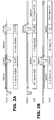
- FIGs. 2A and 2B are diagrams illustrating comparison of a data transmission sequence of an interface device according to an embodiment of the present invention ( FIG. 2B ) with that of an interface device of the related art ( FIG. 2A ).
- the control printed circuit board (CPCB), on which the timing controller 300 is mounted is externally separated from the display module 500, and is connected to a flat flexible cable (FFC) included in the display module 500 by the cable 910.
- the CPCB is built in the above-described host system.
- the above-described system-on-chip (SoC) may also be mounted on the CPCB.
- the power IC, etc. may further be mounted on the FFC of the display module 500.
Landscapes
- Engineering & Computer Science (AREA)
- Physics & Mathematics (AREA)
- Computer Hardware Design (AREA)
- General Physics & Mathematics (AREA)
- Theoretical Computer Science (AREA)
- Control Of Indicators Other Than Cathode Ray Tubes (AREA)
- Control Of El Displays (AREA)
- Electroluminescent Light Sources (AREA)
- Controls And Circuits For Display Device (AREA)
Abstract
Description
- The present invention relates to a display device including an interface device capable of effectively transmitting sensing data for external compensation while using an encrypted transmission technology during communication between a display module and a control module externally separated from the display module for slimness of the display module.
- As the information technology has advanced, the market of display devices as mediums connecting users and information has grown. In line with this, the use of display devices such as liquid crystal displays (LCDs), organic light emitting display devices, electrophoretic displays (EPDs), and plasma display panels (PDPs) has increased.
- Representative examples of flat display devices recently highlighted as display devices to display an image, using digital data, include a liquid crystal display (LCD) using liquid crystals, an organic light emitting diode (OLED) display using OLEDs, and the like.
- An organic light emitting diode (OLED) display device is a self-luminous device in which an organic light emitting layer emits light through re-combination of electrons and holes. Since the OLED display device exhibits high luminance, and uses a low drive voltage while achieving slimness, the OLED display device is expected to be a next-generation display device.
- Such an OLED display device includes a plurality of pixels, each of which includes an OLED constituted by an anode, a cathode, and an organic light emitting layer interposed between the anode and the cathode, and a pixel circuit for independently driving the OLED. The pixel circuit includes a switching thin film transistor (TFT) for supplying a data voltage to a storage capacitor, a drive TFT for controlling drive current in accordance with a drive voltage charged in the storage capacitor, and supplying the controlled drive current to the OLED, and so on. The OLED generates light having a light amount proportional to the amount of the drive current.
- In OLED display devices according to the related art, however, nonuniformity of luminance may occur because there may be deviations of driving characteristics (threshold voltage and mobility) of drive TFTs among pixels due to process deviation and with passage of time. In order to solve such a problem, OLED display devices use an external compensation method for sensing driving characteristics of each pixel, and compensating data to be supplied to the pixel, using the sensed value.
- OLED display devices are applicable to various products such as portable terminals, TV sets, flexible displays, transparent displays, and so on. Recent advances in OLED display devices are focused on slimness, for application of such OLED display devices to a paper display or a wallpaper display.
- For slimness of a display module in an OLED display device, a scheme to externally separate a part of circuit configurations mounted in the display module should be taken into consideration. In this case, an encrypted transmission system is required in order to protect content during communication between the display module and the separated circuit configuration. In particular, when an interface using the encrypted transmission system is used, problems associated with transmission of sensing data required for external compensation of the OLED display device should also be taken into consideration.
- Accordingly, the present invention is directed to an organic light emitting diode (OLED) display device that substantially obviates one or more problems due to limitations and disadvantages of the related art.
- An object of the present invention is to provide an organic light emitting diode display device capable of externally separating a control module from a display module, thereby achieving slimness of the display module.
- Another object of the present invention is to provide an OLED display device including an interface device capable of efficiently transmitting sensing data while using an encrypted transmission protocol for communication between a display module and a control module externally separated from the display module.
- Additional advantages, objects, and features of the invention will be set forth in part in the description which follows and in part will become apparent to those having ordinary skill in the art upon examination of the following or may be learned from practice of the invention. The objectives and other advantages of the invention may be realized and attained by the structure particularly pointed out in the written description and claims hereof as well as the appended drawings.
- To achieve these objects and other advantages and in accordance with the purpose of the invention, as embodied and broadly described herein, an organic light emitting diode (OLED) display device includes a display module comprising a display panel, and a panel driver for driving the display panel, a host system separated from the display module, the host system comprising a timing controller for controlling the panel driver, and an interface device for performing communication between the host system and the display module.
- In the interface device of the OLED display device according to the illustrated embodiment of the present invention, it may be possible to efficiently transmit sensing data in an alternating manner through a plurality of channels respectively using a plurality of vertical synchronization signals respectively processed to have non-overlapping blank periods, such that transmission of the sensing data is carried out in an active period of one channel overlapping with a blank period of another channel.
- In an aspect of the present invention, there is provided an OLED display device including a display module, a host system, and an interface. The display module includes a display panel and a panel driver for driving the display panel. The host system is externally separated from the display module to achieve slimness of the display module. The interface device includes a transmission module configured to transmit sensing data via a plurality of vertical synchronization signals for communication between the host system and the display module. The transmission module generates first and second vertical synchronization signals having blank periods that are not overlapping with each other. The interface device transmits the sensing data in a sensing period of one vertical synchronization signal that overlaps with the blank period of another vertical synchronization signal.
- In another aspect of the present invention, there is provided a method for operating an organic light emitting diode (OLED) display device including a display module, a host system externally separated from the display module, and an interface device including a transmission module configured to transmit sensing data via a plurality of vertical synchronization signals for communication between the host system and the display module. The method includes generating, via the transmission module, first and second vertical synchronization signals having blank periods that are not overlapping with each other, and transmitting, via the interface device, sensing data using an encrypted transmission protocol in a sensing period of one vertical synchronization signal that overlaps with the blank period of another vertical synchronization signal. The method further includes transmitting 3-color RGB data, via a first channel, in an active period of the first vertical synchronization signal and transmitting 1-color W data, via a second channel, in an active period of the second vertical synchronization signal.
- Accordingly, the OLED display device according to the illustrated embodiment of the present invention may not only externally separate the control module from the display module, but also may efficiently transmit sensing data for external compensation in spite of use of an encrypted transmission protocol for protection of externally exposed content, using the above-described interface device. Thus, slimness of the display module may be achieved and, as such, the OLED display device may be applied to a wallpaper display or the like.
- It is to be understood that both the foregoing general description and the following detailed description of the present invention are exemplary and explanatory and are intended to provide further explanation of the invention as claimed.
- The accompanying drawings, which are included to provide a further understanding of the invention and are incorporated in and constitute a part of this application, illustrate embodiments of the invention and along with the description serve to explain the principle of the invention. In the drawings:
-
FIG. 1 is a block diagram schematically illustrating a configuration of an organic light emitting diode (OLED) display device according to an embodiment of the present invention; -
FIGs. 2A and 2B are diagrams illustrating comparison of a data transmission sequence of an interface device according to an embodiment of the present invention (FIG. 2B ) with that of an interface device of the related art (FIG. 2A ); -
FIG. 3 is a diagram illustrating a configuration of a display module illustrated inFIG. 1 ; -
FIG. 4 is a diagram illustrating a slim configuration of the OLED display device according to an embodiment of the present invention; and -
FIG. 5 is a block diagram illustrating an internal configuration of the interface device according to an embodiment of the present invention. - Reference will now be made in detail to the preferred embodiments of the present invention, examples of which are illustrated in the accompanying drawings.
-
FIG. 1 is a block diagram illustrating a configuration of an organic light emitting diode (OLED) display device according to an embodiment of the present invention. - Referring to
FIG 1 , the OLED device includes ahost system 100 and adisplay module 500. - The
display module 500 includes areception module 600, apanel driver 700, and adisplay panel 800. Thehost system 100 includes a system-on-chip (SoC) 200, atiming controller 300, and atransmission module 400. - For slimness of the
display module 500, a control printed circuit board including thetiming controller 300 is separated from thedisplay module 500, and is built in thehost system 100. - For protection of content during communication between the
display module 500 and thetiming controller 300 externally separated from thedisplay module 500, aninterface device 900 using an encrypted transmission system is applied to the OLED display device. In accordance with an embodiment of the present invention, theinterface device 900 includes the transmission module of thehost system 100, and thereception module 600 of thedisplay module 500 connected to thetransmission module 400 via acable 910. Thetransmission module 400 andreception module 600 may be referred to as a "SerDes Tx IC" having an integrated circuit structure and a "SerDes Rx IC" having an integrated circuit structure, respectively. - The
host system 100 may be any one of systems of portable terminals, for example, a computer, a TV system, a set-top box, a tablet, and a portable phone. - The SoC 200 includes a scaler or the like, to convert video data into data having a resolution format suitable for display on the
display module 500, and then to output the converted data to thetiming controller 300. TheSoC 200 generates a plurality of timing signals including a clock CLK, a data enable signal DE, a vertical synchronization signal Vsync, a horizontal synchronization signal Hsync, etc. - The SoC 200 and
timing controller 300 may communicate with each other, using any one of various interfaces. For example, the SoC 200 andtiming controller 300 may transmit and receive data and clocks by use of a low voltage differential signaling (LVDS) interface. In this case, the SoC 200 includes an LVDS transmitter installed at an output stage of theSoC 200, whereas thetiming controller 300 includes an LVDS transmitter installed at an input stage of thetiming controller 300. - The
timing controller 300 converts data of 3 colors (red, green, and blue (RGB)) received from theSoC 200 into data of 4 colors (white, red, green, and blue (WRGB)), using a predetermined RGB-to-WRGB conversion method. Thetiming controller 300 processes the WRGB data through various image processing procedures such as power consumption reduction, picture quality compensation, external compensation, and degradation compensation, and then outputs the resultant data. - For example, for power consumption reduction, the
timing controller 300 analyzes an input image, to determine a peak luminance of the input image in accordance with information as to image characteristics such as average picture level (APL), and adjusts a gamma high-level voltage EVDD in accordance with the determined peak luminance. The adjusted gamma high-level voltage EVDD is then supplied to thedisplay module 500 through theinterface device 900. - For external compensation for deviations among pixels, the
timing controller 300 senses driving characteristics (threshold voltage Vth and mobility of drive TFT, Vth of OLED, etc.) of each pixel in thedisplay panel 800 through theinterface device 900 andpanel driver 700 in every desired sensing period such as a power-on time, a vertical blank period of each vertical synchronization signal, or a power-off time. - For example, in each sensing period, the
timing controller 300 supplies sensing data (data included in video data) to pixels corresponding to the sensing period through theinterface device 900 andpanel driver 700, to drive the pixels. Thepanel driver 700 senses, as a voltage, pixel current reflecting driving characteristics of each driven pixel, and converts the sensed value into a digital sensing value. The digital sensing value from thepanel driver 700 is supplied to thetiming controller 300 through theinterface device 900. - The
timing controller 300 processes the sensing value of each pixel, generates compensation values for compensating for driving deviations of pixels (mobility and Vth deviations of drive TFTs, Vth deviations of OLEDs, etc.), and stores the generated compensation values in a memory. Thetiming controller 300 compensates pixel data to be supplied to the pixels, using the compensation values stored in the memory, and then outputs the compensated pixel data. - The
timing controller 300 generates data control signals and gate control signals for controlling driving timing of thepanel driver 700, using timing signals received from theSoC 200, and outputs the generated control signals to thepanel driver 700 through theinterface device 900. The data control signals may include a source start pulse, a source sampling clock and a source output enable signal for controlling driving timing of a data driver. The gate control signals may include a gate start pulse, a gate shift clock and a gate output enable signal for controlling driving timing of a gate driver. Thetiming controller 300 may transmit the vertical synchronization signal Vsync to thetransmission module 400, together with the above-described control signals. - The
interface device 900 uses a high definition multimedia interface (HDMI) supporting an encryption algorithm for high-bandwidth digital content protection (HDCP) capable of preventing copy of content, in order to protect externally exposed content. The HDMI uses a transition minimized differential signaling (TMDS) communication scheme, which is a digital transmission protocol. - The
transmission module 400 encrypts pixel data received from thetiming controller 300, using the HDCP encryption algorithm, and then converts the encrypted pixel data into a transmission packet, together with control information and so on. A differential signal corresponding to the transmission packet is transmitted from thetransmission module 400 to thereception module 600 in a series manner via thecable 910. Thereception module 600 recovers the transmission packet from the received differential signal, and recovers the pixel data, control information, etc., using an HDCP recovery algorithm. The recovered data is then output from thereception module 600 to thepanel driver 700. -
FIGs. 2A and 2B are diagrams illustrating comparison of a data transmission sequence of an interface device according to an embodiment of the present invention (FIG. 2B ) with that of an interface device of the related art (FIG. 2A ). - In the transition minimized differential signaling (TMDS) communication scheme, as illustrated in
FIG. 2A (related art), it is necessary to transmit RGBW data during an active period Vactive while transmitting various control data CTL and data island DI signals (audio signals or the like) during a blank period Vblank, using the vertical synchronization signal Vsync. For this reason, there is a problem in the related art OLED display devices that it is impossible to transmit sensing data for external compensation in the blank period Vblank. - In order to solve or address this problem, as illustrated in
FIG. 2B , thetransmission module 400 uses vertical synchronization signals Vsync1 and Vsync2 each having a reduced frequency corresponding to 1/2 of the frequency of the input vertical synchronization signal (having a period increased two times) such that each of the vertical synchronization signals Vsync2 and Vsync2 includes an active period Vactive' including pixel data transmission periods for two frames, and a sensing period SD allocated between the pixel data transmission periods. In this case, the sensing period SD of one channel overlaps with the blank period Vblank of another channel. - Accordingly, it may be possible to transmit sensing data, using the sensing period included in the active period of each vertical synchronization signal. In particular, it may be possible to transmit the sensing data by alternating the sensing periods of two channels, namely, first and second channels CH1 and CH2 according to an embodiment of the present invention.
- The
transmission module 400 may increase the transmission rate of RGBW data without frequency increase by transmitting RGB data and W data to thereception module 600 in a separated manner in respective active periods Vactive' of the corresponding vertical synchronization signals Vsync1 and Vsync2, through the first and second channels CH1 and CH2, which use different vertical synchronization signals, namely, the first and second vertical synchronization signals Vsync1 and Vsync2, respectively. Thetransmission module 400 may also transmit additional information CTL/DL including control information CTL and so on in the blank period Vblank. - The
transmission module 400 time-divides the active period Vactive' of the first vertical synchronization signal Vsync1 corresponding to the first channel CH1, and transmits RGB data of N-1-th and N-th frames in the time-divided active periods, respectively. Thetransmission module 400 also time-divides the active period Vactive' of the second vertical synchronization signal Vsync2 corresponding to the second channel CH2, and transmits W data of the N-1-th and N-th frames in the time-divided active periods, respectively. Thetransmission module 400 transmits sensing data in the sensing period SD between the N-1-th and N-th frames corresponding to the first channel CH1, and transmits additional data CTL/DI in the blank period Vblank between the N-1-th and N-th frames corresponding to the second channel CH2. - Thus, the
transmission module 400 may efficiently transmit sensing data to thereception module 600 in the sensing period included in the active period in accordance with frequency and phase adjustment of the vertical synchronization signals. In addition, although each vertical synchronization signal has a frequency reduced by 1/2, transmission of pixel data and additional information may be achieved without frequency change. - The
timing controller 300 andtransmission module 400 transmit and receive data, using any one of various interfaces. Thereception module 600 andpanel driver 700 also transmit and receive data, using any one of various interfaces. - For example, an LVDS interface, an embedded point-to-point interface (EPI) known as a high speed serial interface, or a V-by-one (Vx1) interface may be used. For application of the EPI or Vx1 interface, the transmitter installed at the output stage of the
timing controller 300 or the output stage of thereception module 600 converts pixel data and control information including various control data into a transmission packet having a serial format while including clocks. The transmitter then transmits the transmission packet in the form of a differential signal through a pair of transmission lines. The receiver installed at the input stage of thetransmission module 400 or the input stage of the data driver included in thepanel driver 700 recovers clocks, control information and pixel data from the transmission packet received thereby. The transmission packet includes a control packet including a clock training pattern for clock locking of the receiver, an alignment training pattern, clocks, and control information in the form of serial data, and a data packet including clocks and pixel data in the form of serial data. -
FIG. 3 is a block diagram briefly illustrating a configuration of thedisplay module 500 illustrated inFIG. 1 . - Referring to
FIG. 3 , thedisplay module 500 includes apanel driving unit 700 including the reception (RX)module 600, adata driver 710, and agate driver 720, and thedisplay panel 800. - The
reception module 600 performs data processing required for the differential signal transmitted from thetransmission module 400 via thecable 910, thereby recovering pixel data and control information, as described above. Thereception module 600 converts pixel data and data control information into an EPI packet, and transmits the EPI packet to a plurality ofdata ICs # 1 to #m constituting thedata driver 710. Thereception module 600 transmits a gate control signal to thegate driver 720. The gate control signal may be supplied to thegate driver 720 after being level-shifted while passing through a level shifter included in a power IC. - Each of the
data ICs # 1 to #m constituting thedata driver 710 recovers clocks, control information, and pixel data from the EPI packet transmitted from thereception module 600, converts the pixel data into an analog data signal, and then supplies the analog data signal to corresponding ones of data lines DL included in thedisplay panel 800. Each of thedata ICs # 1 to #m sub-divides a set of reference gamma voltages supplied from a gamma voltage generator separately provided at the outside into grayscale voltages respectively corresponding to grayscale values of pixel data. Each of thedata ICs # 1 to #m is driven in accordance with a data control signal, and converts digital data into an analog data signal, using the sub-divided grayscale voltages, and supplies the analog data signal to the corresponding data lines DL of thedisplay panel 800. Each of thedata ICs # 1 to #m converts sensing pixel data supplied through thereception module 600 in each sensing period into an analog data signal, and supplies the analog data signal to the corresponding pixel P, and senses a voltage according to pixel current reflecting driving characteristics of the corresponding pixel P. Each of thedata ICs # 1 to #m converts the sensed voltage into a digital sensing value, and supplies a differential signal corresponding to the digital sensing value to thetiming controller 300 via theinterface device 900 as shown inFIG. 1 . - Each of the
data ICs # 1 to #m may be mounted on a circuit film such as a tape carrier package (TCP), a chip-on-film (COF), a flexible printed circuit (FPC) or the like, and may then be attached to thedisplay panel 800 in a tape automated bonding (TAB) manner or may be mounted on thedisplay panel 800 in a chip-on-glass (COG) manner. - The
gate driver 720 drives a plurality of gate lines GL included in thedisplay panel 800 in response to gate control signals supplied from thereception module 600. In response to the gate control signals, thegate driver 720 supplies a scan pulse corresponding to a gate-on voltage to each gate line in a scan period corresponding to the gate line, and supplies a gate-off voltage to the gate line in the remaining periods. Thegate driver 720 may be constituted by at least one gate IC. In this case, thegate driver 720 may be mounted on a circuit film such as a TCP, a COF, or an FPC, and may then be attached to thedisplay panel 800 in a TAB manner or may be mounted on thedisplay panel 800 in a COG manner. Otherwise, thegate driver 720 may be formed at a TFT substrate, together with a TFT array constituting a pixel array and, as such, may be installed at a non-display area of thedisplay panel 800 in the form of a gate-in-panel (GIP) type. - The
display panel 800 displays an image through a pixel array in which pixels P are arranged in a matrix form. The pixel array is constituted by W/R/G/B pixels. - Each pixel P includes an OLED connected between a high-level voltage source (EVDD) line and a low-level voltage source (EVSS) line, and a pixel circuit for independently driving the OLED. The pixel circuit includes a first switching TFT ST1, a second switching TFT ST2, a drive TFT DT, and a storage capacitor Cst. The configuration of the pixel circuit may be diverse and, as such, is not limited to the configuration of
FIG. 3 . - The OLED includes an anode connected to the drive TFT DT, a cathode connected to the EVSS line, and a light emitting layer arranged between the anode and the cathode. In accordance with this configuration, the OLED generates light in an amount proportional to the amount of current supplied from the drive TFT DT.
- The first switching TFT ST1 is driven by a gate signal supplied from one gate line GL, and supplies a data signal from a corresponding one of the data lines DL to a gate node of the drive TFT DT. On the other hand, the second switching TFT ST2 is driven by a gate signal supplied from another gate line GL, and supplies a reference voltage from a reference line RL to a source node of the drive TFT DT. The second switching TFT ST2 is also used as a path for outputting current from the drive TFT DT to the reference line RL in a sensing period.
- The storage capacitor Cst, which is connected between the gate and source nodes of the drive TFTs DT, is charged with a differential voltage between the data voltage supplied to the gate node through the first switching TFT ST1 and the reference voltage supplied to the source node through the second switching TFT ST2, and supplies the differential voltage as a drive voltage of the drive TFT DT.
- The drive TFT DT controls current supplied from the high-level voltage source EVDD in accordance with the drive voltage supplied from the storage capacitor Cst and, as such, supplies current proportional to the drive voltage to the OLED which, in turn, emits light.
-
FIG. 4 is a view illustrating a structure of the OLED display device, which achieves slimness in accordance with an embodiment of the present invention. - Referring to
FIG. 4 , the control printed circuit board (CPCB), on which thetiming controller 300 is mounted, is externally separated from thedisplay module 500, and is connected to a flat flexible cable (FFC) included in thedisplay module 500 by thecable 910. The CPCB is built in the above-described host system. The above-described system-on-chip (SoC) may also be mounted on the CPCB. The power IC, etc. may further be mounted on the FFC of thedisplay module 500. - For content protection, the above-described
transmission module 400, namely, a SerDes Tx IC, is mounted on the CPCB, and the above-describedreception module 600, namely, a SerDes Rx IC, is mounted on the FFC. Thetransmission module 400 andreception module 600 communicate with each other through thecable 910 connected between aconnector 920 of the CPCB and aconnector 930 of the FFC in accordance with an HDMI transmission protocol. - The data drivers DD to drive the data lines of the
display panel 800 are connected to thedisplay panel 800. The data drivers DD are connected to a plurality of source printed circuit boards (SPCBs) in a divided manner. Each data driver DD may be constituted by a COF, on which a data IC is mounted. The SPCBs are connected to the FFC via aconnector 940. - The gate drivers GD are connected to opposite lateral sides of the
display panel 800, to drive the gate lines at the opposite sides of thedisplay panel 800. Each gate driver GD may be constituted by a COF, on which a gate IC is mounted. - Thus, in the OLED display device according to the embodiment of the present invention, slimness of the
display module 500 is achieved in accordance with external separation of the CPCB and, as such, the OLED display device may be applied to a wallpaper display or the like. -
FIG. 5 is a block diagram illustrating a configuration of theinterface device 900 according to an embodiment of the present invention. - Referring to
FIG. 5 , thetransmission module 400 includes a receiver (RX) 410, adistributer 420, acompressor 430, a line memory (LM) 440, a synchronization signal (sync)generator 450, anHDCP encoder 460, and an HDMI transmitter (TX) 470. - The
receiver 410 recovers clocks, pixel data and control information from an EPI or Vx1 transmission packet corresponding to a differential signal transmitted from thetiming controller 300, and outputs the recovered data. - The
distributer 420 separates reception data supplied from thereceiver 410 into RGB data, W data, and control information, and outputs the separated data. - The
compressor 430 compresses the RGB data supplied from thedistributer 420, and outputs the compressed data. Theline memory 440 delays the W data supplied from thedistributer 420 for a period in which the RGB data is compressed and, as such, outputs the W data without compression. The RGB data is compressed by thecompressor 430, to reduce the number of bits to be transmitted and, as such, the number of transmission lines may be reduced. - The
synchronization signal generator 450 generates first and second vertical synchronization signals Vsync1 and Vsync2 (cf.FIG. 2B ) having a reduced frequency corresponding to 1/2 of the frequency of an input vertical synchronization signal included in the control information supplied from thedistributer 420, as described above, while having different phases, using the input vertical synchronization signal, and outputs the generated first and second vertical synchronization signals Vsync1 and Vsync2. - The
HDCP encoder 460 encrypts the compressed RGB data supplied from thecompressor 430, and outputs the encrypted data to the first channel CH1 via theHDMI TX 470. TheHDCP encoder 460 also encrypts the non-compressed W data supplied from theline memory LM 440, and outputs the encrypted data to the second channel CH2 via theHDMI TX 470. TheHDMI TX 470 transmits RGB data in an active period of the first vertical synchronization signal Vsync1 through the first channel CH1 in the form of a differential signal while transmitting control information in a blank period of the first vertical synchronization signal Vsync1 in the form of a differential signal. On the other hand, TheHDMI TX 470 transmits W data in an active period of the second vertical synchronization signal Vsync2 through the second channel CH2 in the form of a differential signal while transmitting the control information in a blank period of the second vertical synchronization signal Vsync2 in the form of a differential signal. As described above, theHDMI TX 470 transmits sensing data supplied from theHDCP encoder 460 via the first and second channels CH1 and CH2 in sensing periods corresponding to the first and second channels CH1 and CH2, respectively. - The
reception module 600 includes an HDMI receiver (RX) 610, analigner 620, anHDCP decoder 630, adecompressor 640, aline memory LM 650, aformatter 660, and anEPI transmitter 670. - The
HDMI receiver 610 performs signal processing on differential signals respectively supplied from theHDMI transmitter 470 via the first and second channels CH1 and CH2, thereby recovering clocks, transmission data, and control information. The recovered data is then aligned by thealigner 620, and is then transmitted to theHDCP decoder 630. - The
HDCP decoder 630 recovers RGB data and W data from data output from thealigner 620, and outputs the recovered data. - The
decompressor 640 decompresses the compressed RGB data supplied from theHDCP decoder 630, and outputs the decompressed data. Theline memory 650 outputs the W data supplied from theHDCP decoder 630 after delaying the W data. - The
formatter 660 converts RGBW data supplied from thedecompressor 640 andline memory 650, namely, pixel data and control information, into an EPI transmission packet, together with clocks, and transmits the converted data in the form of a differential signal to each data driver DD via theEPI TX 670. - The
cable 910 connected between thetransmission module 400 and thereception module 600 further includes an additional link. A sensing value supplied from thedata driver 710 in the form of a differential signal is transmitted to thetiming controller 300 via theinterface device 900. - As apparent from the above description, in accordance with the interface device and method in the display device according to the embodiments of the present invention, it may be possible to efficiently transmit sensing data in an alternating manner through a plurality of channels respectively using a plurality of vertical synchronization signals respectively processed to have non-overlapping blank periods, such that transmission of the sensing data is carried out in an active period of one channel overlapping with a blank period of another channel.
- Accordingly, the OLED display device according to the embodiments of the present invention may not only externally separate the control module from the display module, but also may efficiently transmit sensing data for external compensation in spite of use of an encrypted transmission protocol for protection of externally exposed content, using the above-described interface device. Thus, slimness of the display module may be achieved and, as such, the OLED display device may be applied to a wallpaper display or the like.
- It will be apparent to those skilled in the art that various modifications and variations can be made in the present invention without departing from the scope of the inventions. Thus, it is intended that the present invention cover the modifications and variations of this invention provided they come within the scope of the appended claims and their equivalents.
- The following list of embodiments forms part of the description.
- 1. An organic light emitting diode (OLED) display device comprising:
- a display module including a display panel and a panel driver for driving the display panel;
- a host system externally separated from the display module; and
- an interface device including a transmission module configured to transmit sensing data via a plurality of vertical synchronization signals for communication between the host system and the display module,
- wherein the transmission module generates first and second vertical synchronization signals having blank periods that are not overlapping with each other, and
- wherein the interface device transmits the sensing data in a sensing period of one vertical synchronization signal that overlaps with the blank period of another vertical synchronization signal.
- 2. The OLED display device of
embodiment 1, wherein the interface device includes a reception module of the display module, the transmission module embedded in the host system, and a cable connecting the transmission module and the reception module. - 3. The OLED display device of
embodiment 1, wherein the sensing period is included in an active period of the first and second vertical synchronization signals. - 4. The OLED display device of
embodiment 1, wherein the transmission module transmits 3-color RGB data through a first channel in an active period of one vertical synchronization signal, and transmits 1-color W data through a second channel in an active period of another vertical synchronization signal. - 5. The OLED display device of
embodiment 1, wherein the interface device transmits the sensing data using an encrypted transmission protocol. - 6. The OLED display device of embodiment 4, wherein a sensing period of the first channel overlaps with a blank period of the second channel.
- 7. The OLED display device of
embodiment 1, wherein the transmission module transmits control information in a blank period of one vertical synchronization signal which overlaps a sensing period of another vertical synchronization signal. - 8. The OLED display device of
embodiment 1, wherein an active period of the first and second vertical synchronization signals includes pixel data transmission periods for two frames and a sensing period allocated between the pixel data transmission periods. - 9. The OLED display device of embodiment 4, wherein the active period of the first and second vertical synchronization signals alternately has a sensing period in which the sensing data is transmitted.
- 10. The OLED display device of
embodiment 1, wherein the host system includes a computer, a TV set, a set-top box, a tablet, or a portable phone. - 11. An organic light emitting diode (OLED) display device comprising:
- a display module including a panel driver for driving a display panel;
- a control module externally separated from the display module; and
- an interface device including a transmission module configured to transmit sensing data and image data via a plurality of vertical synchronization signals for communication between the control module and the display module,
- wherein the transmission module generates first and second vertical synchronization signals having blank periods that are not overlapping with each other, and
- wherein the interface device transmits the sensing data using an encrypted transmission protocol in a sensing period of one vertical synchronization signal that overlaps with the blank period of another vertical synchronization signal.
- 12. The OLED display device of embodiment 11, wherein the interface device includes a reception module of the display module, the transmission module embedded in the control module, and a cable connecting the transmission module and the reception module.
- 13. The OLED display device of embodiment 11, wherein an active period of one vertical synchronization signal includes pixel data transmission periods for two frames and the sensing period allocated between the pixel data transmission periods.
- 14. The OLED display device of embodiment 11, wherein the transmission module transmits 3-color RGB data through a first channel in an active period of the first vertical synchronization signal, and transmits 1-color W data through a second channel in an active period of the second vertical synchronization signal.
- 15. The OLED display device of embodiment 11, wherein the interface device transmits the sensing data in the sensing period included in an active period of one vertical synchronization signal that overlaps with the blank period of another vertical synchronization signal.
- 16. The OLED display device of embodiment 11, wherein the transmission module transmits control information in the blank period of one vertical synchronization signal which overlaps the sensing period of another vertical synchronization signal.
- 17. The OLED display device of embodiment 14, wherein the transmission modules transmits the sensing data by alternating the sensing periods of the first and second channels.
- 18. The OLED display device of embodiment 14, wherein a sensing period of one channel overlaps with a blank period of another channel.
- 19. The OLED display device of embodiment 11, wherein the control module includes a computer, a TV set, a set-top box, a tablet, or a portable phone.
- 20. A method of operating an organic light emitting diode (OLED) display device including a display module, a host system externally separated from the display module, and an interface device including a transmission module configured to transmit sensing data via a plurality of vertical synchronization signals for communication between the host system and the display module, the method comprising:
- generating, via the transmission module, first and second vertical synchronization signals having blank periods that are not overlapping with each other;
- transmitting, via the interface device, sensing data using an encrypted transmission protocol in a sensing period of one vertical synchronization signal that overlaps with the blank period of another vertical synchronization signal;
- transmitting 3-color RGB data, via a first channel, in an active period of the first vertical synchronization signal; and
- transmitting 1-color W data, via a second channel, in an active period of the second vertical synchronization signal.
Claims (16)
- An organic light emitting diode (OLED) display device comprising:a display module including a panel driver for driving a display panel;a host system, or control module, externally separated from the display module; andan interface device including a transmission module configured to transmit sensing data via a plurality of vertical synchronization signals for communication between the host system and the display module,wherein the transmission module generates first and second vertical synchronization signals having blank periods that are not overlapping with each other, andwherein the interface device transmits the sensing data in a sensing period of one vertical synchronization signal that overlaps with the blank period of another vertical synchronization signal.
- The OLED display device of claim 1, wherein the display module includes the display panel.
- The OLED display device according to any preceding claim, wherein the transmission module is configured to transmit image data via the plurality of vertical synchronization signals.
- The OLED display device of any preceding claim, wherein the interface device includes a reception module of the display module, the transmission module embedded in the host system or the control module, and a cable connecting the transmission module and the reception module.
- The OLED display device of any preceding claim, wherein the sensing period is included in an active period of the first and second vertical synchronization signals.
- The OLED display device of any preceding claim, wherein the transmission module transmits 3-color RGB data through a first channel in an active period of one vertical synchronization signal, possibly the first vertical synchronization signal, and transmits 1-color W data through a second channel in an active period of another vertical synchronization signal, possibly the second vertical synchronization signal.
- The OLED display device of claim 6, wherein a sensing period of the first channel overlaps with a blank period of the second channel.
- The OLED display device of claim 6 or claim 7, wherein the transmission modules transmits the sensing data by alternating the sensing periods of the first and second channels
- The OLED display device of any preceding claim, wherein the interface device transmits the sensing data using an encrypted transmission protocol.
- The OLED display device of any preceding claim, wherein the transmission module transmits control information in a blank period of one vertical synchronization signal which overlaps a sensing period of another vertical synchronization signal.
- The OLED display device of any preceding claim, wherein an active period of one vertical synchronization signal includes pixel data transmission periods for two frames and the sensing period allocated between the pixel data transmission periods.
- The OLED display device of claim 11, wherein an active period of the first and second vertical synchronization signals includes pixel data transmission periods for two frames and a sensing period allocated between the pixel data transmission periods.
- The OLED display device of any preceding claim, wherein the active period of the first and second vertical synchronization signals alternately has a sensing period in which the sensing data is transmitted.
- The OLED display device of any preceding claim, wherein the host system or the control module includes a computer, a TV set, a set-top box, a tablet, or a portable phone.
- The OLED display device of any preceding claim, wherein the interface device transmits the sensing data in the sensing period included in an active period of one vertical synchronization signal that overlaps with the blank period of another vertical synchronization signal.
- A method of operating an organic light emitting diode (OLED) display device including a display module, a host system externally separated from the display module, and an interface device including a transmission module configured to transmit sensing data via a plurality of vertical synchronization signals for communication between the host system and the display module, the method comprising:generating, via the transmission module, first and second vertical synchronization signals having blank periods that are not overlapping with each other;transmitting, via the interface device, sensing data using an encrypted transmission protocol in a sensing period of one vertical synchronization signal that overlaps with the blank period of another vertical synchronization signal;transmitting 3-color RGB data, via a first channel, in an active period of the first vertical synchronization signal; andtransmitting 1-color W data, via a second channel, in an active period of the second vertical synchronization signal.
Applications Claiming Priority (1)
| Application Number | Priority Date | Filing Date | Title |
|---|---|---|---|
| KR1020150152383A KR102406705B1 (en) | 2015-10-30 | 2015-10-30 | Organic light emitting diode display device |
Publications (2)
| Publication Number | Publication Date |
|---|---|
| EP3163564A1 true EP3163564A1 (en) | 2017-05-03 |
| EP3163564B1 EP3163564B1 (en) | 2021-06-09 |
Family
ID=57233317
Family Applications (1)
| Application Number | Title | Priority Date | Filing Date |
|---|---|---|---|
| EP16196473.9A Active EP3163564B1 (en) | 2015-10-30 | 2016-10-28 | Organic light emitting diode display device |
Country Status (5)
| Country | Link |
|---|---|
| US (1) | US10276093B2 (en) |
| EP (1) | EP3163564B1 (en) |
| JP (1) | JP6483649B2 (en) |
| KR (1) | KR102406705B1 (en) |
| CN (1) | CN107045853B (en) |
Cited By (1)
| Publication number | Priority date | Publication date | Assignee | Title |
|---|---|---|---|---|
| CN109389939A (en) * | 2017-08-04 | 2019-02-26 | 乐金显示有限公司 | Communication means and the display device for using the communication means |
Families Citing this family (10)
| Publication number | Priority date | Publication date | Assignee | Title |
|---|---|---|---|---|
| KR102370717B1 (en) * | 2015-12-31 | 2022-03-04 | 엘지디스플레이 주식회사 | Organic light emitting diode display device |
| US10593285B2 (en) | 2017-03-28 | 2020-03-17 | Novatek Microelectronics Corp. | Method and apparatus of handling signal transmission applicable to display system |
| US10504439B2 (en) * | 2017-08-18 | 2019-12-10 | Shenzhen China Star Optoelectronics Semiconductor Display Technology Co., Ltd. | OLED display panel and driving method using differential data for voltage compensation |
| KR102583783B1 (en) * | 2018-08-29 | 2023-10-04 | 엘지디스플레이 주식회사 | Light Emitting Display and Driving Method Thereof |
| KR102696835B1 (en) * | 2018-12-27 | 2024-08-19 | 엘지디스플레이 주식회사 | Organic light emitting diode display device |
| CN110111718A (en) * | 2019-05-07 | 2019-08-09 | 深圳市华星光电技术有限公司 | The control method and electronic equipment of a kind of electronic equipment |
| KR102657135B1 (en) * | 2019-05-15 | 2024-04-15 | 삼성디스플레이 주식회사 | Transceiver system |
| US11341904B2 (en) * | 2019-08-13 | 2022-05-24 | Novatek Microelectronics Corp. | Light-emitting diode driving apparatus and light-emitting diode driver |
| KR102893019B1 (en) * | 2020-03-16 | 2025-12-02 | 삼성디스플레이 주식회사 | Display device and driving method thereof |
| CN114968151B (en) * | 2021-02-26 | 2025-01-21 | 凌巨科技股份有限公司 | Multi-screen display system |
Citations (1)
| Publication number | Priority date | Publication date | Assignee | Title |
|---|---|---|---|---|
| US6564269B1 (en) * | 1998-09-10 | 2003-05-13 | Silicon Image, Inc. | Bi-directional data transfer using the video blanking period in a digital data stream |
Family Cites Families (12)
| Publication number | Priority date | Publication date | Assignee | Title |
|---|---|---|---|---|
| US6989827B2 (en) * | 2002-10-24 | 2006-01-24 | Hewlett-Packard Development Company, Lp. | System and method for transferring data through a video interface |
| US20060269056A1 (en) * | 2005-05-19 | 2006-11-30 | Bruce Montag | Messaging interface for protected digital outputs |
| US7639244B2 (en) * | 2005-06-15 | 2009-12-29 | Chi Mei Optoelectronics Corporation | Flat panel display using data drivers with low electromagnetic interference |
| WO2007096961A1 (en) * | 2006-02-22 | 2007-08-30 | Fujitsu Hitachi Plasma Display Limited | Plasma display device and display method thereof |
| JP2007322501A (en) * | 2006-05-30 | 2007-12-13 | Canon Inc | Active matrix substrate, reflective liquid crystal display device, and projection display device |
| KR101480001B1 (en) * | 2008-02-26 | 2015-01-09 | 삼성디스플레이 주식회사 | Organic light emminting display device and processing method image signals thereof |
| KR101598396B1 (en) * | 2009-11-27 | 2016-03-15 | 삼성디스플레이 주식회사 | Method for displaying stereo-scopic image and display apparatus for performing the same |
| KR20120065840A (en) * | 2010-12-13 | 2012-06-21 | 삼성전자주식회사 | Display driver circuit, operating method thereof, and user device including that |
| KR101463651B1 (en) | 2011-10-12 | 2014-11-20 | 엘지디스플레이 주식회사 | Organic light-emitting display device |
| KR101470688B1 (en) * | 2011-12-08 | 2014-12-08 | 엘지디스플레이 주식회사 | Organic Light Emitting Display And Compensation Method Of Degradation Thereof |
| US8946994B2 (en) | 2012-09-25 | 2015-02-03 | Lg Display Co., Ltd. | Organic light emitting display device and driving method thereof |
| CN202841323U (en) | 2012-10-10 | 2013-03-27 | 西安诺瓦电子科技有限公司 | High-speed data transmission and processing device |
-
2015
- 2015-10-30 KR KR1020150152383A patent/KR102406705B1/en active Active
-
2016
- 2016-10-25 JP JP2016208449A patent/JP6483649B2/en active Active
- 2016-10-27 US US15/336,513 patent/US10276093B2/en active Active
- 2016-10-28 EP EP16196473.9A patent/EP3163564B1/en active Active
- 2016-10-28 CN CN201610971456.1A patent/CN107045853B/en active Active
Patent Citations (1)
| Publication number | Priority date | Publication date | Assignee | Title |
|---|---|---|---|---|
| US6564269B1 (en) * | 1998-09-10 | 2003-05-13 | Silicon Image, Inc. | Bi-directional data transfer using the video blanking period in a digital data stream |
Non-Patent Citations (1)
| Title |
|---|
| LEMME H: "OLEDS - SENKRECHTSTARTER AUS KUNSTSTOFF BESTE AUSSICHTEN FUER DISPLAYS AUS ORGANISCHEN LEUCHTDIODEN", ELEKTRONIK, W E K A FACHZEITSCHRIFTEN-VERLAG GMBH, DE, vol. 49, no. 2, 25 January 2000 (2000-01-25), pages 97 - 103, XP000945626, ISSN: 0013-5658 * |
Cited By (1)
| Publication number | Priority date | Publication date | Assignee | Title |
|---|---|---|---|---|
| CN109389939A (en) * | 2017-08-04 | 2019-02-26 | 乐金显示有限公司 | Communication means and the display device for using the communication means |
Also Published As
| Publication number | Publication date |
|---|---|
| US10276093B2 (en) | 2019-04-30 |
| CN107045853A (en) | 2017-08-15 |
| CN107045853B (en) | 2019-07-19 |
| JP2017083836A (en) | 2017-05-18 |
| KR102406705B1 (en) | 2022-06-08 |
| JP6483649B2 (en) | 2019-03-13 |
| US20170124949A1 (en) | 2017-05-04 |
| KR20170050613A (en) | 2017-05-11 |
| EP3163564B1 (en) | 2021-06-09 |
Similar Documents
| Publication | Publication Date | Title |
|---|---|---|
| US10013906B2 (en) | Organic light emitting diode display device | |
| US10276093B2 (en) | Organic light emitting diode display device using vertical synchronization signals with different phase | |
| US11443710B2 (en) | Display interface device capable of reducing power consumption | |
| US10249258B2 (en) | Display interface device and data transmission method thereof | |
| KR102176504B1 (en) | Display device and method for driving the same | |
| KR102126546B1 (en) | Interface apparatus and method of display device | |
| KR102531321B1 (en) | Organic Light Emitting Diode Display Device and Method for driving the same | |
| US10614763B2 (en) | Communication method and display device using the same | |
| KR20210081905A (en) | Display apparatus | |
| US20130127804A1 (en) | Data driving apparatus, display device including the same, and driving method thereof | |
| KR102270604B1 (en) | Image display system | |
| KR102494149B1 (en) | Data driving circuit and image display device | |
| KR20150135615A (en) | Display device and method of driving the same | |
| KR20160092155A (en) | Display Device | |
| KR102840997B1 (en) | Multivision system | |
| KR102362743B1 (en) | Communication method and display device using the same | |
| US12223220B2 (en) | Display module, and method for transmitting control signal for display module | |
| US10971087B2 (en) | Display device and method of driving the same | |
| KR102232869B1 (en) | Data interface apparatus and method, image display system using the same, and driving method thereof | |
| KR20240122166A (en) | Display Apparatus | |
| KR20240120469A (en) | Display Apparatus | |
| KR20130067106A (en) | Usb interface board and display device using the same |
Legal Events
| Date | Code | Title | Description |
|---|---|---|---|
| PUAI | Public reference made under article 153(3) epc to a published international application that has entered the european phase |
Free format text: ORIGINAL CODE: 0009012 |
|
| STAA | Information on the status of an ep patent application or granted ep patent |
Free format text: STATUS: THE APPLICATION HAS BEEN PUBLISHED |
|
| AK | Designated contracting states |
Kind code of ref document: A1 Designated state(s): AL AT BE BG CH CY CZ DE DK EE ES FI FR GB GR HR HU IE IS IT LI LT LU LV MC MK MT NL NO PL PT RO RS SE SI SK SM TR |
|
| AX | Request for extension of the european patent |
Extension state: BA ME |
|
| STAA | Information on the status of an ep patent application or granted ep patent |
Free format text: STATUS: REQUEST FOR EXAMINATION WAS MADE |
|
| 17P | Request for examination filed |
Effective date: 20171031 |
|
| RBV | Designated contracting states (corrected) |
Designated state(s): AL AT BE BG CH CY CZ DE DK EE ES FI FR GB GR HR HU IE IS IT LI LT LU LV MC MK MT NL NO PL PT RO RS SE SI SK SM TR |
|
| STAA | Information on the status of an ep patent application or granted ep patent |
Free format text: STATUS: EXAMINATION IS IN PROGRESS |
|
| 17Q | First examination report despatched |
Effective date: 20180712 |
|
| GRAP | Despatch of communication of intention to grant a patent |
Free format text: ORIGINAL CODE: EPIDOSNIGR1 |
|
| STAA | Information on the status of an ep patent application or granted ep patent |
Free format text: STATUS: GRANT OF PATENT IS INTENDED |
|
| INTG | Intention to grant announced |
Effective date: 20210112 |
|
| GRAS | Grant fee paid |
Free format text: ORIGINAL CODE: EPIDOSNIGR3 |
|
| GRAA | (expected) grant |
Free format text: ORIGINAL CODE: 0009210 |
|
| STAA | Information on the status of an ep patent application or granted ep patent |
Free format text: STATUS: THE PATENT HAS BEEN GRANTED |
|
| AK | Designated contracting states |
Kind code of ref document: B1 Designated state(s): AL AT BE BG CH CY CZ DE DK EE ES FI FR GB GR HR HU IE IS IT LI LT LU LV MC MK MT NL NO PL PT RO RS SE SI SK SM TR |
|
| REG | Reference to a national code |
Ref country code: GB Ref legal event code: FG4D |
|
| REG | Reference to a national code |
Ref country code: CH Ref legal event code: EP Ref country code: AT Ref legal event code: REF Ref document number: 1401148 Country of ref document: AT Kind code of ref document: T Effective date: 20210615 |
|
| REG | Reference to a national code |
Ref country code: DE Ref legal event code: R096 Ref document number: 602016059068 Country of ref document: DE |
|
| REG | Reference to a national code |
Ref country code: IE Ref legal event code: FG4D |
|
| REG | Reference to a national code |
Ref country code: LT Ref legal event code: MG9D |
|
| PG25 | Lapsed in a contracting state [announced via postgrant information from national office to epo] |
Ref country code: LT Free format text: LAPSE BECAUSE OF FAILURE TO SUBMIT A TRANSLATION OF THE DESCRIPTION OR TO PAY THE FEE WITHIN THE PRESCRIBED TIME-LIMIT Effective date: 20210609 Ref country code: FI Free format text: LAPSE BECAUSE OF FAILURE TO SUBMIT A TRANSLATION OF THE DESCRIPTION OR TO PAY THE FEE WITHIN THE PRESCRIBED TIME-LIMIT Effective date: 20210609 Ref country code: BG Free format text: LAPSE BECAUSE OF FAILURE TO SUBMIT A TRANSLATION OF THE DESCRIPTION OR TO PAY THE FEE WITHIN THE PRESCRIBED TIME-LIMIT Effective date: 20210909 Ref country code: HR Free format text: LAPSE BECAUSE OF FAILURE TO SUBMIT A TRANSLATION OF THE DESCRIPTION OR TO PAY THE FEE WITHIN THE PRESCRIBED TIME-LIMIT Effective date: 20210609 |
|
| REG | Reference to a national code |
Ref country code: AT Ref legal event code: MK05 Ref document number: 1401148 Country of ref document: AT Kind code of ref document: T Effective date: 20210609 |
|
| REG | Reference to a national code |
Ref country code: NL Ref legal event code: MP Effective date: 20210609 |
|
| PG25 | Lapsed in a contracting state [announced via postgrant information from national office to epo] |
Ref country code: GR Free format text: LAPSE BECAUSE OF FAILURE TO SUBMIT A TRANSLATION OF THE DESCRIPTION OR TO PAY THE FEE WITHIN THE PRESCRIBED TIME-LIMIT Effective date: 20210910 Ref country code: LV Free format text: LAPSE BECAUSE OF FAILURE TO SUBMIT A TRANSLATION OF THE DESCRIPTION OR TO PAY THE FEE WITHIN THE PRESCRIBED TIME-LIMIT Effective date: 20210609 Ref country code: NO Free format text: LAPSE BECAUSE OF FAILURE TO SUBMIT A TRANSLATION OF THE DESCRIPTION OR TO PAY THE FEE WITHIN THE PRESCRIBED TIME-LIMIT Effective date: 20210909 Ref country code: RS Free format text: LAPSE BECAUSE OF FAILURE TO SUBMIT A TRANSLATION OF THE DESCRIPTION OR TO PAY THE FEE WITHIN THE PRESCRIBED TIME-LIMIT Effective date: 20210609 Ref country code: SE Free format text: LAPSE BECAUSE OF FAILURE TO SUBMIT A TRANSLATION OF THE DESCRIPTION OR TO PAY THE FEE WITHIN THE PRESCRIBED TIME-LIMIT Effective date: 20210609 |
|
| PG25 | Lapsed in a contracting state [announced via postgrant information from national office to epo] |
Ref country code: EE Free format text: LAPSE BECAUSE OF FAILURE TO SUBMIT A TRANSLATION OF THE DESCRIPTION OR TO PAY THE FEE WITHIN THE PRESCRIBED TIME-LIMIT Effective date: 20210609 Ref country code: CZ Free format text: LAPSE BECAUSE OF FAILURE TO SUBMIT A TRANSLATION OF THE DESCRIPTION OR TO PAY THE FEE WITHIN THE PRESCRIBED TIME-LIMIT Effective date: 20210609 Ref country code: SM Free format text: LAPSE BECAUSE OF FAILURE TO SUBMIT A TRANSLATION OF THE DESCRIPTION OR TO PAY THE FEE WITHIN THE PRESCRIBED TIME-LIMIT Effective date: 20210609 Ref country code: SK Free format text: LAPSE BECAUSE OF FAILURE TO SUBMIT A TRANSLATION OF THE DESCRIPTION OR TO PAY THE FEE WITHIN THE PRESCRIBED TIME-LIMIT Effective date: 20210609 Ref country code: AT Free format text: LAPSE BECAUSE OF FAILURE TO SUBMIT A TRANSLATION OF THE DESCRIPTION OR TO PAY THE FEE WITHIN THE PRESCRIBED TIME-LIMIT Effective date: 20210609 Ref country code: NL Free format text: LAPSE BECAUSE OF FAILURE TO SUBMIT A TRANSLATION OF THE DESCRIPTION OR TO PAY THE FEE WITHIN THE PRESCRIBED TIME-LIMIT Effective date: 20210609 Ref country code: PT Free format text: LAPSE BECAUSE OF FAILURE TO SUBMIT A TRANSLATION OF THE DESCRIPTION OR TO PAY THE FEE WITHIN THE PRESCRIBED TIME-LIMIT Effective date: 20211011 Ref country code: RO Free format text: LAPSE BECAUSE OF FAILURE TO SUBMIT A TRANSLATION OF THE DESCRIPTION OR TO PAY THE FEE WITHIN THE PRESCRIBED TIME-LIMIT Effective date: 20210609 Ref country code: ES Free format text: LAPSE BECAUSE OF FAILURE TO SUBMIT A TRANSLATION OF THE DESCRIPTION OR TO PAY THE FEE WITHIN THE PRESCRIBED TIME-LIMIT Effective date: 20210609 |
|
| PG25 | Lapsed in a contracting state [announced via postgrant information from national office to epo] |
Ref country code: PL Free format text: LAPSE BECAUSE OF FAILURE TO SUBMIT A TRANSLATION OF THE DESCRIPTION OR TO PAY THE FEE WITHIN THE PRESCRIBED TIME-LIMIT Effective date: 20210609 |
|
| REG | Reference to a national code |
Ref country code: DE Ref legal event code: R097 Ref document number: 602016059068 Country of ref document: DE |
|
| PLBE | No opposition filed within time limit |
Free format text: ORIGINAL CODE: 0009261 |
|
| STAA | Information on the status of an ep patent application or granted ep patent |
Free format text: STATUS: NO OPPOSITION FILED WITHIN TIME LIMIT |
|
| PG25 | Lapsed in a contracting state [announced via postgrant information from national office to epo] |
Ref country code: DK Free format text: LAPSE BECAUSE OF FAILURE TO SUBMIT A TRANSLATION OF THE DESCRIPTION OR TO PAY THE FEE WITHIN THE PRESCRIBED TIME-LIMIT Effective date: 20210609 |
|
| 26N | No opposition filed |
Effective date: 20220310 |
|
| REG | Reference to a national code |
Ref country code: CH Ref legal event code: PL |
|
| PG25 | Lapsed in a contracting state [announced via postgrant information from national office to epo] |
Ref country code: AL Free format text: LAPSE BECAUSE OF FAILURE TO SUBMIT A TRANSLATION OF THE DESCRIPTION OR TO PAY THE FEE WITHIN THE PRESCRIBED TIME-LIMIT Effective date: 20210609 |
|
| REG | Reference to a national code |
Ref country code: BE Ref legal event code: MM Effective date: 20211031 |
|
| PG25 | Lapsed in a contracting state [announced via postgrant information from national office to epo] |
Ref country code: MC Free format text: LAPSE BECAUSE OF FAILURE TO SUBMIT A TRANSLATION OF THE DESCRIPTION OR TO PAY THE FEE WITHIN THE PRESCRIBED TIME-LIMIT Effective date: 20210609 |
|
| PG25 | Lapsed in a contracting state [announced via postgrant information from national office to epo] |
Ref country code: LU Free format text: LAPSE BECAUSE OF NON-PAYMENT OF DUE FEES Effective date: 20211028 Ref country code: IT Free format text: LAPSE BECAUSE OF FAILURE TO SUBMIT A TRANSLATION OF THE DESCRIPTION OR TO PAY THE FEE WITHIN THE PRESCRIBED TIME-LIMIT Effective date: 20210609 Ref country code: BE Free format text: LAPSE BECAUSE OF NON-PAYMENT OF DUE FEES Effective date: 20211031 |
|
| PG25 | Lapsed in a contracting state [announced via postgrant information from national office to epo] |
Ref country code: LI Free format text: LAPSE BECAUSE OF NON-PAYMENT OF DUE FEES Effective date: 20211031 Ref country code: CH Free format text: LAPSE BECAUSE OF NON-PAYMENT OF DUE FEES Effective date: 20211031 |
|
| PG25 | Lapsed in a contracting state [announced via postgrant information from national office to epo] |
Ref country code: IE Free format text: LAPSE BECAUSE OF NON-PAYMENT OF DUE FEES Effective date: 20211028 |
|
| PG25 | Lapsed in a contracting state [announced via postgrant information from national office to epo] |
Ref country code: HU Free format text: LAPSE BECAUSE OF FAILURE TO SUBMIT A TRANSLATION OF THE DESCRIPTION OR TO PAY THE FEE WITHIN THE PRESCRIBED TIME-LIMIT; INVALID AB INITIO Effective date: 20161028 |
|
| PG25 | Lapsed in a contracting state [announced via postgrant information from national office to epo] |
Ref country code: CY Free format text: LAPSE BECAUSE OF FAILURE TO SUBMIT A TRANSLATION OF THE DESCRIPTION OR TO PAY THE FEE WITHIN THE PRESCRIBED TIME-LIMIT Effective date: 20210609 |
|
| PG25 | Lapsed in a contracting state [announced via postgrant information from national office to epo] |
Ref country code: MK Free format text: LAPSE BECAUSE OF FAILURE TO SUBMIT A TRANSLATION OF THE DESCRIPTION OR TO PAY THE FEE WITHIN THE PRESCRIBED TIME-LIMIT Effective date: 20210609 |
|
| PG25 | Lapsed in a contracting state [announced via postgrant information from national office to epo] |
Ref country code: TR Free format text: LAPSE BECAUSE OF FAILURE TO SUBMIT A TRANSLATION OF THE DESCRIPTION OR TO PAY THE FEE WITHIN THE PRESCRIBED TIME-LIMIT Effective date: 20210609 |
|
| PG25 | Lapsed in a contracting state [announced via postgrant information from national office to epo] |
Ref country code: MT Free format text: LAPSE BECAUSE OF FAILURE TO SUBMIT A TRANSLATION OF THE DESCRIPTION OR TO PAY THE FEE WITHIN THE PRESCRIBED TIME-LIMIT Effective date: 20210609 |
|
| PGFP | Annual fee paid to national office [announced via postgrant information from national office to epo] |
Ref country code: GB Payment date: 20250820 Year of fee payment: 10 |
|
| PGFP | Annual fee paid to national office [announced via postgrant information from national office to epo] |
Ref country code: FR Payment date: 20250821 Year of fee payment: 10 |
|
| PGFP | Annual fee paid to national office [announced via postgrant information from national office to epo] |
Ref country code: DE Payment date: 20250820 Year of fee payment: 10 |