EP3161925B1 - Dreistufige leistungstopologie - Google Patents
Dreistufige leistungstopologie Download PDFInfo
- Publication number
- EP3161925B1 EP3161925B1 EP14896115.4A EP14896115A EP3161925B1 EP 3161925 B1 EP3161925 B1 EP 3161925B1 EP 14896115 A EP14896115 A EP 14896115A EP 3161925 B1 EP3161925 B1 EP 3161925B1
- Authority
- EP
- European Patent Office
- Prior art keywords
- switch
- power
- bus
- coupled
- switching
- Prior art date
- Legal status (The legal status is an assumption and is not a legal conclusion. Google has not performed a legal analysis and makes no representation as to the accuracy of the status listed.)
- Active
Links
Images


Classifications
-
- H—ELECTRICITY
- H02—GENERATION; CONVERSION OR DISTRIBUTION OF ELECTRIC POWER
- H02M—APPARATUS FOR CONVERSION BETWEEN AC AND AC, BETWEEN AC AND DC, OR BETWEEN DC AND DC, AND FOR USE WITH MAINS OR SIMILAR POWER SUPPLY SYSTEMS; CONVERSION OF DC OR AC INPUT POWER INTO SURGE OUTPUT POWER; CONTROL OR REGULATION THEREOF
- H02M5/00—Conversion of AC power input into AC power output, e.g. for change of voltage, for change of frequency, for change of number of phases
- H02M5/40—Conversion of AC power input into AC power output, e.g. for change of voltage, for change of frequency, for change of number of phases with intermediate conversion into DC
- H02M5/42—Conversion of AC power input into AC power output, e.g. for change of voltage, for change of frequency, for change of number of phases with intermediate conversion into DC by static converters
- H02M5/44—Conversion of AC power input into AC power output, e.g. for change of voltage, for change of frequency, for change of number of phases with intermediate conversion into DC by static converters using discharge tubes or semiconductor devices to convert the intermediate DC into AC
- H02M5/453—Conversion of AC power input into AC power output, e.g. for change of voltage, for change of frequency, for change of number of phases with intermediate conversion into DC by static converters using discharge tubes or semiconductor devices to convert the intermediate DC into AC using devices of a triode or transistor type requiring continuous application of a control signal
- H02M5/458—Conversion of AC power input into AC power output, e.g. for change of voltage, for change of frequency, for change of number of phases with intermediate conversion into DC by static converters using discharge tubes or semiconductor devices to convert the intermediate DC into AC using devices of a triode or transistor type requiring continuous application of a control signal using semiconductor devices only
- H02M5/4585—Conversion of AC power input into AC power output, e.g. for change of voltage, for change of frequency, for change of number of phases with intermediate conversion into DC by static converters using discharge tubes or semiconductor devices to convert the intermediate DC into AC using devices of a triode or transistor type requiring continuous application of a control signal using semiconductor devices only having a rectifier with controlled elements
-
- H—ELECTRICITY
- H02—GENERATION; CONVERSION OR DISTRIBUTION OF ELECTRIC POWER
- H02M—APPARATUS FOR CONVERSION BETWEEN AC AND AC, BETWEEN AC AND DC, OR BETWEEN DC AND DC, AND FOR USE WITH MAINS OR SIMILAR POWER SUPPLY SYSTEMS; CONVERSION OF DC OR AC INPUT POWER INTO SURGE OUTPUT POWER; CONTROL OR REGULATION THEREOF
- H02M7/00—Conversion of AC power input into DC power output; Conversion of DC power input into AC power output
- H02M7/42—Conversion of DC power input into AC power output without possibility of reversal
- H02M7/44—Conversion of DC power input into AC power output without possibility of reversal by static converters
- H02M7/48—Conversion of DC power input into AC power output without possibility of reversal by static converters using discharge tubes with control electrode or semiconductor devices with control electrode
- H02M7/483—Converters with outputs that each can have more than two voltages levels
- H02M7/487—Neutral point clamped inverters
-
- H—ELECTRICITY
- H02—GENERATION; CONVERSION OR DISTRIBUTION OF ELECTRIC POWER
- H02J—ELECTRIC POWER NETWORKS; CIRCUIT ARRANGEMENTS OR SYSTEMS FOR SUPPLYING OR DISTRIBUTING ELECTRIC POWER; SYSTEMS FOR STORING ELECTRIC ENERGY
- H02J9/00—Circuit arrangements for emergency or stand-by power supply, e.g. for emergency lighting
- H02J9/04—Circuit arrangements for emergency or stand-by power supply, e.g. for emergency lighting in which the distribution system is disconnected from the normal source and connected to a standby source
- H02J9/06—Circuit arrangements for emergency or stand-by power supply, e.g. for emergency lighting in which the distribution system is disconnected from the normal source and connected to a standby source with automatic change-over, e.g. UPS systems
- H02J9/062—Circuit arrangements for emergency or stand-by power supply, e.g. for emergency lighting in which the distribution system is disconnected from the normal source and connected to a standby source with automatic change-over, e.g. UPS systems for AC powered loads
- H02J9/063—Common neutral, e.g. AC input neutral line connected to AC output neutral line and DC middle point
-
- H—ELECTRICITY
- H02—GENERATION; CONVERSION OR DISTRIBUTION OF ELECTRIC POWER
- H02M—APPARATUS FOR CONVERSION BETWEEN AC AND AC, BETWEEN AC AND DC, OR BETWEEN DC AND DC, AND FOR USE WITH MAINS OR SIMILAR POWER SUPPLY SYSTEMS; CONVERSION OF DC OR AC INPUT POWER INTO SURGE OUTPUT POWER; CONTROL OR REGULATION THEREOF
- H02M1/00—Details of apparatus for conversion
- H02M1/0048—Circuits or arrangements for reducing losses
- H02M1/0054—Transistor switching losses
- H02M1/0058—Transistor switching losses by employing soft switching techniques, i.e. commutation of transistors when applied voltage is zero or when current flow is zero
-
- H—ELECTRICITY
- H02—GENERATION; CONVERSION OR DISTRIBUTION OF ELECTRIC POWER
- H02M—APPARATUS FOR CONVERSION BETWEEN AC AND AC, BETWEEN AC AND DC, OR BETWEEN DC AND DC, AND FOR USE WITH MAINS OR SIMILAR POWER SUPPLY SYSTEMS; CONVERSION OF DC OR AC INPUT POWER INTO SURGE OUTPUT POWER; CONTROL OR REGULATION THEREOF
- H02M1/00—Details of apparatus for conversion
- H02M1/42—Circuits or arrangements for compensating for or adjusting power factor in converters or inverters
- H02M1/4208—Arrangements for improving power factor of AC input
- H02M1/4216—Arrangements for improving power factor of AC input operating from a three-phase input voltage
-
- Y—GENERAL TAGGING OF NEW TECHNOLOGICAL DEVELOPMENTS; GENERAL TAGGING OF CROSS-SECTIONAL TECHNOLOGIES SPANNING OVER SEVERAL SECTIONS OF THE IPC; TECHNICAL SUBJECTS COVERED BY FORMER USPC CROSS-REFERENCE ART COLLECTIONS [XRACs] AND DIGESTS
- Y02—TECHNOLOGIES OR APPLICATIONS FOR MITIGATION OR ADAPTATION AGAINST CLIMATE CHANGE
- Y02B—CLIMATE CHANGE MITIGATION TECHNOLOGIES RELATED TO BUILDINGS, e.g. HOUSING, HOUSE APPLIANCES OR RELATED END-USER APPLICATIONS
- Y02B70/00—Technologies for an efficient end-user side electric power management and consumption
- Y02B70/10—Technologies improving the efficiency by using switched-mode power supplies [SMPS], i.e. efficient power electronics conversion e.g. power factor correction or reduction of losses in power supplies or efficient standby modes
Definitions
- first DC switch circuit comprises a DC switch coupled between the first DC bus and the neutral point, and a diode coupled in parallel with the DC switch between the first DC bus and the neutral point, wherein in operating the first DC switch circuit such that voltage on the first DC bus is zero, the controller is further configured to operate the DC switch to turn off.
- the controller is further configured to synchronize the turn-on switching of the at least one first switch with the turn-off switching of the at least one second switch over a synchronized switching period.
- the controller is further configured to turn off the DC switch at a first time before the synchronized switching period.
- a new 3-level UPS topology that reduces overall switching losses (i.e., provides higher efficiency) is described herein.
- the 3-level UPS topology introduces Zero Voltage Switching (ZVS) at PFC switch turn on and also at inverter switch turn-off, thus reducing switching losses and enabling higher overall efficiency.
- ZVS Zero Voltage Switching
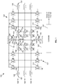
- the collector of the third switch 116 is also coupled to the second terminal of the first inductor 108.
- the emitter of the third switch 116 is coupled to the emitter of the fourth switch 118.
- the collector of the fourth switch 118 is coupled to the neutral point 144.
- the collector of the eighth switch 126 is coupled to the neutral point 144.
- the emitter of the eighth switch 126 is coupled to the emitter of the seventh switch 124.
- the collector of the seventh switch 124 is also coupled to the first terminal of the second inductor 146.
- the source of the ninth switch 128 is coupled to the positive "floating" DC bus 140.
- the drain of the ninth switch 128 is coupled to the positive DC bus 136.
- the controller 152 also operates the switches 112-130 to provide ZVS when the PFC zero-point switch (i.e., the third switch 116) is turned on and when the inverter switch (i.e., the fifth switch 120) is turned off.
- the controller 152 synchronizes the PFC zero-point switch and the inverter switch so that the PFC zero-point switch (i.e., the third switch 116) turns on and the inverter switch (i.e., the fifth switch 120) turns off during a synchronized switching period.
- the PFC zero-point switch is turned on and the inverter switch is turned off at substantially the same time.
- the PFC zero-point switch may be turned on a relatively short time before the inverter switch is turned off.
- FIG. 2 includes graphs illustrating switching cycles of the UPS 100 according to at least one embodiment.
- FIG. 2 includes a first graph 200 illustrating different currents in the UPS 100 over multiple switching cycles of the UPS 100 and a second graph 250 illustrating different control signals of the UPS 100 over multiple switching cycles of the UPS 100.
- a high control signal 252 from the controller 152 turns on the PFC zero-point switch (i.e., the third switch 116 or fourth switch 118).
- a low control signal 254 from the controller turns off the inverter switch (i.e., the fifth switch 120 or sixth switch 122).
- the delay between the first time 208 and the second time 210 is around 500ns; however, in other embodiments, the delay between the first time 208 and the second time 210 may be defined differently.
- the DC switches i.e., the ninth switch 128 and the tenth switch 130
- the DC switches are turned off before the synchronized switching period of the PFC zero-point switches and the inverter switches (i.e., at the third time 212) and turned on after the synchronized switching period (i.e., at the fourth time 214).
- the DC switches are delivering power to the "floating" DC busses 140, 142 (e.g., at the third time 212)
- the voltage on the "floating" DC busses 140, 142 drops to zero.
- switching of the PFC zero-point switch (i.e., the third switch 116 or fourth switch 118) and the inverter switch (i.e., the fifth switch 120 or sixth switch 122) of a segment 102, 104, 106 of the UPS 100 is synchronized during a switching period; however, where the UPS 100 is a 3-phase UPS, the switching of PFC zero-point switches and inverter switches across all three phases of the UPS is synchronized so that all PFC zero-point switches (i.e., the third switch 116 or fourth switch 118es) in the UPS 100 turn on at the same time , or a little before, all of the inverter switches (i.e., the fifth switch 120 or sixth switch 122) in the UPS 100 turn off.
- the UPS 100 is a 3-phase UPS
- the DC switches i.e., the ninth switch 128 and the tenth switch 130
- each segment 102, 104, 106 i.e., each phase
- the DC switches are operated to introduce ZVS at PFC switch turn on and inverter switch turn off across each phase (i.e., in each segment) of the UPS 100.
- the system 500 may include for example a general-purpose computing platform such as those based on Intel PENTIUM-type processor, Motorola PowerPC, Sun UltraSPARC, Texas Instruments-DSP, Hewlett-Packard PA-RISC processors, or any other type of processor.
- System 500 may include specially-programmed, special-purpose hardware, for example, an application-specific integrated circuit (ASIC).
- ASIC application-specific integrated circuit
- Various aspects of the present disclosure may be implemented as specialized software executing on the system 500 such as that shown in FIG. 5 .
- the processor 506 may manipulate the data within the integrated circuit memory 510 and then copy the data to the storage 512 after processing is completed.
- a variety of mechanisms are known for managing data movement between storage 512 and the integrated circuit memory element 510, and the disclosure is not limited thereto. The disclosure is not limited to a particular memory system 510 or a storage system 512.
- the processor and operating system together may form a computer platform for which application programs in high-level programming languages may be written. It should be understood that the disclosure is not limited to a particular computer system platform, processor, operating system, or network. Also, it should be apparent to those skilled in the art that the present disclosure is not limited to a specific programming language or computer system. Further, it should be appreciated that other appropriate programming languages and other appropriate computer systems could also be used.
- At least some embodiments described herein provide a 3-level UPS topology that reduces overall switching losses (i.e., provides higher efficiency).
- the 3-level UPS topology introduces ZVS through the operation of DC switch circuits "in series” with the DC-busses that are “shared” by all phases of the UPS.
- the "shared" DC switch circuits are operated to drive voltage across PFC switches to zero during switch turn-on and to drive voltage across inverter switches to zero during switch turn-off, thus reducing switching losses and enabling higher overall efficiency with a limited number of additional components.
Landscapes
- Engineering & Computer Science (AREA)
- Power Engineering (AREA)
- Inverter Devices (AREA)
Claims (12)
- Ein Leistungsversorgungssystem (100), das Folgendes beinhaltet:einen Eingang, der konfiguriert ist, um Wechselstromeingangsleistung von einer Eingangsleistungsquelle zu empfangen;einen Ausgang, der konfiguriert ist, um einer Last Wechselstromausgangsleistung bereitzustellen;einen Wandler (101), der mit dem Eingang gekoppelt ist und konfiguriert ist, um die Wechselstromeingangsleistung in umgewandelte Gleichstromleistung umzuwandeln, wobei der Wandler (101) mindestens einen ersten Schalter (116, 118) umfasst, der zwischen dem Eingang und einem Neutralpunkt (144) gekoppelt ist, und wobei der Wandler konfiguriert ist, um einen Eingangsstrom von dem Eingang zu empfangen;einen ersten Gleichstrombus (140), der mit dem Wandler gekoppelt ist und konfiguriert ist, um die umgewandelte Gleichstromleistung zu empfangen;einen Wechselrichter (103), der mit dem ersten Gleichstrombus und dem Ausgang gekoppelt ist und konfiguriert ist, um Gleichstromleistung von dem ersten Gleichstrombus in die Wechselstromausgangsleistung umzuwandeln, wobei der Wechselrichter mindestens einen zweiten Schalter (120, 122) umfasst, der zwischen dem ersten Gleichstrombus und dem Ausgang gekoppelt ist, wobei der Wechselrichter ferner mindestens einen dritten Schalter (124, 126) umfasst, der zwischen dem Neutralpunkt und dem Ausgang gekoppelt ist, und wobei der Wechselrichter konfiguriert ist, um dem Ausgang einen Ausgangsstrom bereitzustellen;einen ersten Gleichstromschalterstromkreis (105), der zwischen dem ersten Gleichstrombus und dem Neutralpunkt gekoppelt ist;einen Kondensator (C1), der über den ersten Gleichstromschalterstromkreis selektiv mit dem ersten Gleichstrombus gekoppelt ist; undeine Steuerung (152), die mit dem ersten Gleichstromschalterstromkreis gekoppelt ist und konfiguriert ist, um das Schalten des mindestens einen ersten Schalters zu betätigen, um die Gleichstromleistung zu erzeugen, um das Schalten des mindestens einen zweiten Schalters und des mindestens einen dritten Schalters zu betätigen, um die Wechselstromausgangsleistung zu erzeugen, und die ferner konfiguriert ist, um den Gleichstromschalterstromkreis zu einem ersten Zeitpunkt vor der synchronisierten Schaltdauer des Einschaltschaltens des mindestens einen ersten Schalters und Ausschaltschaltens des mindestens einen zweiten Schalters auszuschalten, sodass die Spannung auf dem ersten Gleichstrombus relativ zu dem Neutralpunkt während der Schaltbetätigung des mindestens einen ersten Schalters und des mindestens einen zweiten Schalters null ist, wenn der Ausgangsstrom höher als der Eingangsstrom ist, sodass die Spannung entlang dem mindestens einen ersten Schalter während des Einschaltschaltens null ist und die Spannung entlang dem mindestens einen zweiten Schalter während des Ausschaltschaltens null ist.
- Leistungsversorgungssystem gemäß Anspruch 1, wobei der erste Gleichstromschalterstromkreis Folgendes beinhaltet:einen Gleichstromschalter, der zwischen dem ersten Gleichstrombus und dem Neutralpunkt gekoppelt ist; undeine Diode, die parallel zu dem Gleichstromschalter zwischen dem ersten Gleichstrombus und dem Neutralpunkt gekoppelt ist,wobei beim Betätigen des ersten Gleichstromschalterstromkreises, sodass die Spannung auf dem ersten Gleichstrombus relativ zu dem Neutralpunkt null ist, die Steuerung ferner konfiguriert ist, um den Gleichstromschalter zu betätigen, sich auszuschalten.
- Leistungsversorgungssystem gemäß Anspruch 2, wobei die Steuerung ferner konfiguriert ist, um das Einschaltschalten des mindestens einen ersten Schalters über eine synchronisierte Schaltdauer mit dem Ausschaltschalten des mindestens einen zweiten Schalters zu synchronisieren.
- Leistungsversorgungssystem gemäß Anspruch 1, wobei das Leistungsversorgungssystem ferner Folgendes beinhaltet:einen zweiten Gleichstrombus, der zwischen dem Kondensator und dem ersten Gleichstromschalterstromkreis gekoppelt ist,wobei zu dem ersten Zeitpunkt vor der synchronisierten Schaltdauer die Gleichstromleistung, die von dem Wechselrichter in die Wechselstromausgangsleistung umgewandelt wird, von der umgewandelten Gleichstromleistung und der Gleichstromleistung von dem zweiten Gleichstrombus abgeleitet ist.
- Leistungsversorgungssystem gemäß Anspruch 1, das ferner Folgendes beinhaltet:mindestens eine Gleichstromeingangsleitung, die konfiguriert ist, um mit einer Gleichstromquelle gekoppelt zu sein; undeinen Gleichstrom-Gleichstrom-Wandler, der zwischen der mindestens einen Gleichstromeingangsleitung und dem ersten Gleichstrombus gekoppelt ist und konfiguriert ist, um Gleichstromreserveleistung von der Gleichstromquelle zu empfangen und dem ersten Gleichstrombus geregelte Gleichstromleistung bereitzustellen,wobei die Gleichstromleistung, die von dem Wechselrichter in die Wechselstromausgangsleistung umgewandelt wird, von mindestens einer von der umgewandelten Gleichstromleistung und der Gleichstromreserveleistung abgeleitet ist.
- Leistungsversorgungssystem gemäß Anspruch 5, wobei der Gleichstrom-Gleichstrom-Wandler Folgendes beinhaltet:
mindestens einen ersten Gleichstrom-Gleichstrom-Schalter, der zwischen der mindestens einen Gleichstromeingangsleitung und dem Neutralpunkt gekoppelt ist, wobei die Steuerung ferner mit dem mindestens einen ersten Gleichstrom-Gleichstrom-Schalter gekoppelt ist und ferner konfiguriert ist, wo die Gleichstromleistung, die von dem Wechselrichter in die Wechselstromausgangsleistung umgewandelt wird, von der Gleichstromreserveleistung abgeleitet ist, um den mindestens einen ersten Gleichstrom-Gleichstrom-Schalter zu betätigen, um die geregelte Gleichstromleistung zu erzeugen, und den ersten Gleichstromschalterstromkreis zu betätigen, sodass die Spannung entlang des mindestens einen ersten Gleichstrom-Gleichstrom-Schalters während des Einschaltens null ist. - Leistungsversorgungssystem gemäß Anspruch 6, wobei der Gleichstrom-Gleichstrom-Wandler Folgendes beinhaltet:mindestens einen zweiten Gleichstrom-Gleichstrom-Schalter, der zwischen der mindestens einen Gleichstromeingangsleitung und dem ersten Gleichstrombus gekoppelt ist,wobei die Steuerung ferner mit dem mindestens einen zweiten Gleichstrom-Gleichstrom-Schalter gekoppelt ist und ferner konfiguriert ist, wo die Gleichstromleistung, die von dem Wechselrichter in die Wechselstromausgangsleistung umgewandelt wird, von der umgewandelten Gleichstromleistung abgeleitet ist, um den mindestens einen zweiten Gleichstrom-Gleichstrom-Schalter zu betätigen, um Batterieladeleistung aus der umgewandelten Gleichstromleistung zu erzeugen, und den ersten Gleichstromschalterstromkreis zu betätigen, sodass die Spannung entlang des mindestens einen zweiten Gleichstrom-Gleichstrom-Schalters während des Ausschaltens null ist.
- Leistungsversorgungssystem gemäß Anspruch 1, wobei das Leistungsversorgungssystem ein Dreiphasenleistungsversorgungssystem ist, das mehrere Abschnitte umfasst, wobei jeder Abschnitt konfiguriert ist, um mit einer Phase der Dreiphasenleistung, die von der Eingangsleistungsquelle empfangen wird, betätigt zu werden,
wobei der erste Gleichstromschalterstromkreis von mehreren Abschnitten des Dreiphasenleistungsversorgungssystems geteilt wird und
wobei die Steuerung ferner konfiguriert ist, um die Schaltbetätigung des Wandlers und des Wechselrichters entlang jedem Abschnitt des Leistungsversorgungssystems zu synchronisieren. - Ein Verfahren zum Betätigen eines Leistungsversorgungssystems gemäß Anspruch 1, wobei das Verfahren Folgendes beinhaltet:Empfangen, an dem Eingang, von Wechselstromeingangsleistung, die einem Eingangsstrom von einer Leistungsquelle entspricht;Umwandeln, mit dem Wandler, der Wechselstromeingangsleistung in umgewandelte Gleichstromleistung;Bereitstellen der umgewandelten Gleichstromleistung für den ersten Gleichstrombus; Umwandeln, mit dem Wandler, von Gleichstromleistung von dem ersten Gleichstrombus in Wechselstromausgangsleistung, die einem Ausgangsstrom entspricht;Bereitstellen der Wechselstromausgangsleistung für den Ausgang; undSteuern des Leistungsversorgungssystems, sodass die Spannung auf dem ersten Gleichstrombus relativ zu dem Neutralpunk gegen Null geht, um in dem mindestens einen ersten Schalter und dem mindestens einen zweiten Schalter spannungsfreies Schalten bereitzustellen, wenn der Ausgangsstrom höher als der Eingangsstrom ist, wobei das Steuern das selektive Entkoppeln des Kondensators von dem ersten Gleichstrombus umfasst.
- Verfahren gemäß Anspruch 9,
wobei das Umwandeln der Wechselstromeingangsleistung das Schalten des mindestens einen ersten Schalters des Wandlers umfasst, um die umgewandelte Gleichstromleistung zu erzeugen;
wobei das Umwandeln von Gleichstromleistung von dem ersten Gleichstrombus das Schalten des mindestens einen zweiten Schalters des Wandlers umfasst, um die Wechselstromausgangsleistung zu erzeugen; und
wobei das Steuern des Leistungsversorgungssystems, sodass die Spannung auf dem ersten Gleichstrombus relativ zu dem Neutralpunkt gegen Null geht, das Treiben der Spannung entlang dem mindestens einen ersten Schalter auf Null während des Einschaltschaltens und der Spannung entlang dem mindestens einen zweiten Schalter auf Null während des Ausschaltschaltens umfasst. - Verfahren gemäß Anspruch 10,
wobei das Leistungsversorgungssystem ferner einen ersten Gleichstromschalter beinhaltet, der zwischen dem Neutralpunkt und dem ersten Gleichstrombus gekoppelt ist, und wobei das Treiben der Spannung entlang dem mindestens einen ersten Schalter auf Null und der Spannung entlang dem mindestens einen zweiten Schalter auf Null das Ausschalten des ersten Gleichstromschalters umfasst. - Verfahren gemäß Anspruch 11,
das ferner das Synchronisieren des Einschaltschaltens des mindestens einen ersten Schalters mit dem Ausschaltschalten des mindestens einen zweiten Schalters über eine synchronisierte Schaltdauer beinhaltet, wobei das Ausschalten des ersten Gleichstromschalters das Ausschalten des ersten Gleichstromschalters zu einem ersten Zeitpunkt vor der synchronisierten Schaltdauer umfasst, wenn der Ausgangsstrom höher als der Eingangsstrom ist.
Applications Claiming Priority (1)
| Application Number | Priority Date | Filing Date | Title |
|---|---|---|---|
| PCT/US2014/044551 WO2015199718A1 (en) | 2014-06-27 | 2014-06-27 | 3-level power topology |
Publications (3)
| Publication Number | Publication Date |
|---|---|
| EP3161925A1 EP3161925A1 (de) | 2017-05-03 |
| EP3161925A4 EP3161925A4 (de) | 2018-03-07 |
| EP3161925B1 true EP3161925B1 (de) | 2021-08-04 |
Family
ID=54938628
Family Applications (1)
| Application Number | Title | Priority Date | Filing Date |
|---|---|---|---|
| EP14896115.4A Active EP3161925B1 (de) | 2014-06-27 | 2014-06-27 | Dreistufige leistungstopologie |
Country Status (4)
| Country | Link |
|---|---|
| US (1) | US9979313B2 (de) |
| EP (1) | EP3161925B1 (de) |
| CN (1) | CN106663940B (de) |
| WO (1) | WO2015199718A1 (de) |
Families Citing this family (18)
| Publication number | Priority date | Publication date | Assignee | Title |
|---|---|---|---|---|
| KR102166362B1 (ko) * | 2013-12-18 | 2020-10-15 | 오티스 엘리베이터 컴파니 | 다중-레벨 회생 드라이브를 위한 버스 커패시터 뱅크 구성 |
| WO2015167568A1 (en) * | 2014-05-01 | 2015-11-05 | Schneider Electric It Corporation | Power supply control |
| CN107546836B (zh) * | 2016-06-23 | 2019-11-26 | 维谛技术有限公司 | 一种ups电源 |
| US10211672B2 (en) * | 2016-10-13 | 2019-02-19 | Schneider Electric It Corporation | DC-link bus balancer |
| US10461575B2 (en) * | 2017-03-28 | 2019-10-29 | Schneider Electric It Corporation | Multistate PWM command for 3 levels inverters |
| CN110829571B (zh) * | 2018-08-09 | 2024-03-15 | 施耐德电气It公司 | 高效柔性转换器 |
| DE102018119916A1 (de) | 2018-08-16 | 2020-02-20 | Eaton Intelligent Power Limited | Elektrische AC/DC-Umwandlungs-Anordnung |
| JP7066051B2 (ja) | 2018-09-13 | 2022-05-12 | エルエス、エレクトリック、カンパニー、リミテッド | 電源供給装置及び電源供給システム |
| KR102299860B1 (ko) * | 2018-09-13 | 2021-09-09 | 엘에스일렉트릭 (주) | 전원 공급 장치 및 전원 공급 시스템 |
| US10439512B1 (en) * | 2018-09-27 | 2019-10-08 | Schneider Electric It Corporation | Clamp circuit to reduce overshoot in power converters |
| TWI676341B (zh) * | 2018-11-13 | 2019-11-01 | 新唐科技股份有限公司 | 穩壓系統 |
| US10784714B2 (en) | 2018-11-30 | 2020-09-22 | Schneider Electric It Corporation | 3 phase UPS bus balancer |
| US11050338B2 (en) * | 2018-11-30 | 2021-06-29 | Schneider Electric It Corporation | Detection of shoot-through in power converters |
| CN111509992B (zh) * | 2020-04-30 | 2021-09-07 | 华为技术有限公司 | 交流电源电路、其控制方法及交流电源 |
| CN113924724B (zh) | 2020-04-30 | 2024-11-22 | 华为数字能源技术有限公司 | 一种电力电子变压器及供电系统 |
| KR20220169774A (ko) * | 2021-06-21 | 2022-12-28 | 휴렛-팩커드 디벨롭먼트 컴퍼니, 엘.피. | 화성 형성 장치의 변환기 출력 스위치 실패모드시 보호장치 |
| KR102923053B1 (ko) * | 2021-06-28 | 2026-02-04 | 현대자동차 주식회사 | 충전 장치 |
| CN119341059B (zh) * | 2024-10-23 | 2026-01-27 | 郭文勇 | 部分功率控制型储能系统的拓扑结构和调制方法 |
Family Cites Families (13)
| Publication number | Priority date | Publication date | Assignee | Title |
|---|---|---|---|---|
| US4730242A (en) | 1986-09-25 | 1988-03-08 | Wisconsin Alumni Research Foundation | Static power conversion and apparatus having essentially zero switching losses |
| US5017800A (en) * | 1989-09-29 | 1991-05-21 | Wisconsin Alumni Research Foundation | AC to DC to AC power conversion apparatus with few active switches and input and output control |
| US5982646A (en) * | 1998-06-30 | 1999-11-09 | General Electric Company | Voltage clamp snubbers for three level converter |
| US20060152085A1 (en) * | 2004-10-20 | 2006-07-13 | Fred Flett | Power system method and apparatus |
| US7126833B2 (en) * | 2004-11-24 | 2006-10-24 | Ut-Battelle, Llc | Auxiliary quasi-resonant dc tank electrical power converter |
| WO2007003544A2 (de) * | 2005-06-30 | 2007-01-11 | Siemens Aktiengesellschaft | Frequenzumrichter mit kondensatorlosem spannungs-zwischenkreis |
| US7573732B2 (en) * | 2007-05-25 | 2009-08-11 | General Electric Company | Protective circuit and method for multi-level converter |
| US9118259B2 (en) | 2007-12-03 | 2015-08-25 | Texas Instruments Incorporated | Phase-shifted dual-bridge DC/DC converter with wide-range ZVS and zero circulating current |
| JP5304192B2 (ja) * | 2008-03-28 | 2013-10-02 | ダイキン工業株式会社 | 電力変換装置 |
| WO2010021052A1 (ja) | 2008-08-22 | 2010-02-25 | 東芝三菱電機産業システム株式会社 | 電力変換装置 |
| JP5947109B2 (ja) | 2012-05-24 | 2016-07-06 | 株式会社日立製作所 | 無停電電源装置、無停電電源装置の制御方法 |
| WO2015065363A1 (en) | 2013-10-30 | 2015-05-07 | Schneider Electric It Corporation | Power supply control |
| US20160049892A1 (en) * | 2014-08-18 | 2016-02-18 | Baker Hughes Incorporated | Systems and Methods for Variable Speed Drives |
-
2014
- 2014-06-27 EP EP14896115.4A patent/EP3161925B1/de active Active
- 2014-06-27 WO PCT/US2014/044551 patent/WO2015199718A1/en not_active Ceased
- 2014-06-27 CN CN201480080551.1A patent/CN106663940B/zh active Active
- 2014-06-27 US US15/320,622 patent/US9979313B2/en active Active
Non-Patent Citations (1)
| Title |
|---|
| None * |
Also Published As
| Publication number | Publication date |
|---|---|
| US20170149346A1 (en) | 2017-05-25 |
| EP3161925A1 (de) | 2017-05-03 |
| WO2015199718A1 (en) | 2015-12-30 |
| CN106663940B (zh) | 2019-08-06 |
| US9979313B2 (en) | 2018-05-22 |
| CN106663940A (zh) | 2017-05-10 |
| EP3161925A4 (de) | 2018-03-07 |
Similar Documents
| Publication | Publication Date | Title |
|---|---|---|
| US9979313B2 (en) | 3-level power topology | |
| AU2012302148B2 (en) | Twin boost converter with integrated charger for ups | |
| US9203323B2 (en) | Very high efficiency uninterruptible power supply | |
| US10033269B2 (en) | Voltage doubler with capacitor module for increasing capacitance | |
| US10033264B2 (en) | Bulk capacitor switching for power converters | |
| US11196338B2 (en) | Semiconductor topologies and devices for soft starting and active fault protection of power converters | |
| CN107947338B (zh) | Dc链路总线平衡器 | |
| EP3629459A1 (de) | Snubberschaltung zur reduzierung des überschwingens in stromrichtern | |
| US11811235B2 (en) | Inverter apparatus and power supply system | |
| JPWO2015056571A1 (ja) | 電力変換装置及び電力変換方法 | |
| US20120019230A1 (en) | Dc/dc converter circuit and method for controlling a dc/dc converter circuit | |
| EP3480934B1 (de) | Bidirektionaler dc-ac-wandler mit zwei richtungen | |
| US20210288487A1 (en) | Motor drive device, blower, compressor, and air conditioner | |
| US20220173652A1 (en) | Power conversion system and virtual dc voltage generator circuit | |
| US8787055B2 (en) | Inverter device | |
| US9673692B2 (en) | Application of normally closed power semiconductor devices | |
| US10630195B2 (en) | Converter and power conversion device using same | |
| US10033299B2 (en) | Converter and power conversion device including the same | |
| US9853572B2 (en) | Bridge leg circuit | |
| US11444547B2 (en) | Power conversion apparatus | |
| EP3100346B1 (de) | Unidirektionaler matrixumrichter mit regenerationssystem | |
| US20170302084A1 (en) | Control of freewheeling voltage | |
| US12375004B2 (en) | Synchronous reverse blocking switch for soft-switching current source converters and soft-switching current source converters including the same | |
| JP6241253B2 (ja) | 共振型インバータ装置 | |
| WO2019049301A1 (ja) | コンバータおよびそれを用いた無停電電源装置 |
Legal Events
| Date | Code | Title | Description |
|---|---|---|---|
| STAA | Information on the status of an ep patent application or granted ep patent |
Free format text: STATUS: THE INTERNATIONAL PUBLICATION HAS BEEN MADE |
|
| PUAI | Public reference made under article 153(3) epc to a published international application that has entered the european phase |
Free format text: ORIGINAL CODE: 0009012 |
|
| STAA | Information on the status of an ep patent application or granted ep patent |
Free format text: STATUS: REQUEST FOR EXAMINATION WAS MADE |
|
| 17P | Request for examination filed |
Effective date: 20161215 |
|
| AK | Designated contracting states |
Kind code of ref document: A1 Designated state(s): AL AT BE BG CH CY CZ DE DK EE ES FI FR GB GR HR HU IE IS IT LI LT LU LV MC MK MT NL NO PL PT RO RS SE SI SK SM TR |
|
| AX | Request for extension of the european patent |
Extension state: BA ME |
|
| DAX | Request for extension of the european patent (deleted) | ||
| A4 | Supplementary search report drawn up and despatched |
Effective date: 20180205 |
|
| RIC1 | Information provided on ipc code assigned before grant |
Ipc: H02M 1/42 20070101ALI20180130BHEP Ipc: H02J 9/06 20060101ALI20180130BHEP Ipc: H02J 3/00 20060101AFI20180130BHEP Ipc: H02M 5/458 20060101ALI20180130BHEP Ipc: H02M 1/00 20060101ALI20180130BHEP Ipc: H02M 7/487 20070101ALI20180130BHEP |
|
| STAA | Information on the status of an ep patent application or granted ep patent |
Free format text: STATUS: EXAMINATION IS IN PROGRESS |
|
| 17Q | First examination report despatched |
Effective date: 20190607 |
|
| GRAP | Despatch of communication of intention to grant a patent |
Free format text: ORIGINAL CODE: EPIDOSNIGR1 |
|
| STAA | Information on the status of an ep patent application or granted ep patent |
Free format text: STATUS: GRANT OF PATENT IS INTENDED |
|
| INTG | Intention to grant announced |
Effective date: 20210125 |
|
| GRAS | Grant fee paid |
Free format text: ORIGINAL CODE: EPIDOSNIGR3 |
|
| GRAA | (expected) grant |
Free format text: ORIGINAL CODE: 0009210 |
|
| STAA | Information on the status of an ep patent application or granted ep patent |
Free format text: STATUS: THE PATENT HAS BEEN GRANTED |
|
| RAP3 | Party data changed (applicant data changed or rights of an application transferred) |
Owner name: SCHNEIDER ELECTRIC IT CORPORATION |
|
| AK | Designated contracting states |
Kind code of ref document: B1 Designated state(s): AL AT BE BG CH CY CZ DE DK EE ES FI FR GB GR HR HU IE IS IT LI LT LU LV MC MK MT NL NO PL PT RO RS SE SI SK SM TR |
|
| REG | Reference to a national code |
Ref country code: GB Ref legal event code: FG4D |
|
| REG | Reference to a national code |
Ref country code: AT Ref legal event code: REF Ref document number: 1417986 Country of ref document: AT Kind code of ref document: T Effective date: 20210815 |
|
| REG | Reference to a national code |
Ref country code: CH Ref legal event code: EP |
|
| REG | Reference to a national code |
Ref country code: DE Ref legal event code: R096 Ref document number: 602014079289 Country of ref document: DE |
|
| REG | Reference to a national code |
Ref country code: IE Ref legal event code: FG4D |
|
| REG | Reference to a national code |
Ref country code: LT Ref legal event code: MG9D |
|
| REG | Reference to a national code |
Ref country code: NL Ref legal event code: MP Effective date: 20210804 |
|
| REG | Reference to a national code |
Ref country code: AT Ref legal event code: MK05 Ref document number: 1417986 Country of ref document: AT Kind code of ref document: T Effective date: 20210804 |
|
| PG25 | Lapsed in a contracting state [announced via postgrant information from national office to epo] |
Ref country code: BG Free format text: LAPSE BECAUSE OF FAILURE TO SUBMIT A TRANSLATION OF THE DESCRIPTION OR TO PAY THE FEE WITHIN THE PRESCRIBED TIME-LIMIT Effective date: 20211104 Ref country code: AT Free format text: LAPSE BECAUSE OF FAILURE TO SUBMIT A TRANSLATION OF THE DESCRIPTION OR TO PAY THE FEE WITHIN THE PRESCRIBED TIME-LIMIT Effective date: 20210804 Ref country code: LT Free format text: LAPSE BECAUSE OF FAILURE TO SUBMIT A TRANSLATION OF THE DESCRIPTION OR TO PAY THE FEE WITHIN THE PRESCRIBED TIME-LIMIT Effective date: 20210804 Ref country code: NO Free format text: LAPSE BECAUSE OF FAILURE TO SUBMIT A TRANSLATION OF THE DESCRIPTION OR TO PAY THE FEE WITHIN THE PRESCRIBED TIME-LIMIT Effective date: 20211104 Ref country code: PT Free format text: LAPSE BECAUSE OF FAILURE TO SUBMIT A TRANSLATION OF THE DESCRIPTION OR TO PAY THE FEE WITHIN THE PRESCRIBED TIME-LIMIT Effective date: 20211206 Ref country code: FI Free format text: LAPSE BECAUSE OF FAILURE TO SUBMIT A TRANSLATION OF THE DESCRIPTION OR TO PAY THE FEE WITHIN THE PRESCRIBED TIME-LIMIT Effective date: 20210804 Ref country code: ES Free format text: LAPSE BECAUSE OF FAILURE TO SUBMIT A TRANSLATION OF THE DESCRIPTION OR TO PAY THE FEE WITHIN THE PRESCRIBED TIME-LIMIT Effective date: 20210804 Ref country code: HR Free format text: LAPSE BECAUSE OF FAILURE TO SUBMIT A TRANSLATION OF THE DESCRIPTION OR TO PAY THE FEE WITHIN THE PRESCRIBED TIME-LIMIT Effective date: 20210804 Ref country code: RS Free format text: LAPSE BECAUSE OF FAILURE TO SUBMIT A TRANSLATION OF THE DESCRIPTION OR TO PAY THE FEE WITHIN THE PRESCRIBED TIME-LIMIT Effective date: 20210804 Ref country code: SE Free format text: LAPSE BECAUSE OF FAILURE TO SUBMIT A TRANSLATION OF THE DESCRIPTION OR TO PAY THE FEE WITHIN THE PRESCRIBED TIME-LIMIT Effective date: 20210804 |
|
| PG25 | Lapsed in a contracting state [announced via postgrant information from national office to epo] |
Ref country code: PL Free format text: LAPSE BECAUSE OF FAILURE TO SUBMIT A TRANSLATION OF THE DESCRIPTION OR TO PAY THE FEE WITHIN THE PRESCRIBED TIME-LIMIT Effective date: 20210804 Ref country code: LV Free format text: LAPSE BECAUSE OF FAILURE TO SUBMIT A TRANSLATION OF THE DESCRIPTION OR TO PAY THE FEE WITHIN THE PRESCRIBED TIME-LIMIT Effective date: 20210804 Ref country code: GR Free format text: LAPSE BECAUSE OF FAILURE TO SUBMIT A TRANSLATION OF THE DESCRIPTION OR TO PAY THE FEE WITHIN THE PRESCRIBED TIME-LIMIT Effective date: 20211105 |
|
| PG25 | Lapsed in a contracting state [announced via postgrant information from national office to epo] |
Ref country code: NL Free format text: LAPSE BECAUSE OF FAILURE TO SUBMIT A TRANSLATION OF THE DESCRIPTION OR TO PAY THE FEE WITHIN THE PRESCRIBED TIME-LIMIT Effective date: 20210804 |
|
| PG25 | Lapsed in a contracting state [announced via postgrant information from national office to epo] |
Ref country code: DK Free format text: LAPSE BECAUSE OF FAILURE TO SUBMIT A TRANSLATION OF THE DESCRIPTION OR TO PAY THE FEE WITHIN THE PRESCRIBED TIME-LIMIT Effective date: 20210804 |
|
| REG | Reference to a national code |
Ref country code: DE Ref legal event code: R097 Ref document number: 602014079289 Country of ref document: DE |
|
| PG25 | Lapsed in a contracting state [announced via postgrant information from national office to epo] |
Ref country code: SM Free format text: LAPSE BECAUSE OF FAILURE TO SUBMIT A TRANSLATION OF THE DESCRIPTION OR TO PAY THE FEE WITHIN THE PRESCRIBED TIME-LIMIT Effective date: 20210804 Ref country code: SK Free format text: LAPSE BECAUSE OF FAILURE TO SUBMIT A TRANSLATION OF THE DESCRIPTION OR TO PAY THE FEE WITHIN THE PRESCRIBED TIME-LIMIT Effective date: 20210804 Ref country code: RO Free format text: LAPSE BECAUSE OF FAILURE TO SUBMIT A TRANSLATION OF THE DESCRIPTION OR TO PAY THE FEE WITHIN THE PRESCRIBED TIME-LIMIT Effective date: 20210804 Ref country code: EE Free format text: LAPSE BECAUSE OF FAILURE TO SUBMIT A TRANSLATION OF THE DESCRIPTION OR TO PAY THE FEE WITHIN THE PRESCRIBED TIME-LIMIT Effective date: 20210804 Ref country code: CZ Free format text: LAPSE BECAUSE OF FAILURE TO SUBMIT A TRANSLATION OF THE DESCRIPTION OR TO PAY THE FEE WITHIN THE PRESCRIBED TIME-LIMIT Effective date: 20210804 Ref country code: AL Free format text: LAPSE BECAUSE OF FAILURE TO SUBMIT A TRANSLATION OF THE DESCRIPTION OR TO PAY THE FEE WITHIN THE PRESCRIBED TIME-LIMIT Effective date: 20210804 |
|
| PLBE | No opposition filed within time limit |
Free format text: ORIGINAL CODE: 0009261 |
|
| STAA | Information on the status of an ep patent application or granted ep patent |
Free format text: STATUS: NO OPPOSITION FILED WITHIN TIME LIMIT |
|
| 26N | No opposition filed |
Effective date: 20220506 |
|
| PG25 | Lapsed in a contracting state [announced via postgrant information from national office to epo] |
Ref country code: IT Free format text: LAPSE BECAUSE OF FAILURE TO SUBMIT A TRANSLATION OF THE DESCRIPTION OR TO PAY THE FEE WITHIN THE PRESCRIBED TIME-LIMIT Effective date: 20210804 |
|
| PG25 | Lapsed in a contracting state [announced via postgrant information from national office to epo] |
Ref country code: SI Free format text: LAPSE BECAUSE OF FAILURE TO SUBMIT A TRANSLATION OF THE DESCRIPTION OR TO PAY THE FEE WITHIN THE PRESCRIBED TIME-LIMIT Effective date: 20210804 |
|
| PG25 | Lapsed in a contracting state [announced via postgrant information from national office to epo] |
Ref country code: MC Free format text: LAPSE BECAUSE OF FAILURE TO SUBMIT A TRANSLATION OF THE DESCRIPTION OR TO PAY THE FEE WITHIN THE PRESCRIBED TIME-LIMIT Effective date: 20210804 |
|
| REG | Reference to a national code |
Ref country code: CH Ref legal event code: PL |
|
| REG | Reference to a national code |
Ref country code: BE Ref legal event code: MM Effective date: 20220630 |
|
| PG25 | Lapsed in a contracting state [announced via postgrant information from national office to epo] |
Ref country code: LU Free format text: LAPSE BECAUSE OF NON-PAYMENT OF DUE FEES Effective date: 20220627 Ref country code: LI Free format text: LAPSE BECAUSE OF NON-PAYMENT OF DUE FEES Effective date: 20220630 Ref country code: IE Free format text: LAPSE BECAUSE OF NON-PAYMENT OF DUE FEES Effective date: 20220627 Ref country code: CH Free format text: LAPSE BECAUSE OF NON-PAYMENT OF DUE FEES Effective date: 20220630 |
|
| PG25 | Lapsed in a contracting state [announced via postgrant information from national office to epo] |
Ref country code: BE Free format text: LAPSE BECAUSE OF NON-PAYMENT OF DUE FEES Effective date: 20220630 |
|
| PG25 | Lapsed in a contracting state [announced via postgrant information from national office to epo] |
Ref country code: HU Free format text: LAPSE BECAUSE OF FAILURE TO SUBMIT A TRANSLATION OF THE DESCRIPTION OR TO PAY THE FEE WITHIN THE PRESCRIBED TIME-LIMIT; INVALID AB INITIO Effective date: 20140627 |
|
| PG25 | Lapsed in a contracting state [announced via postgrant information from national office to epo] |
Ref country code: MK Free format text: LAPSE BECAUSE OF FAILURE TO SUBMIT A TRANSLATION OF THE DESCRIPTION OR TO PAY THE FEE WITHIN THE PRESCRIBED TIME-LIMIT Effective date: 20210804 Ref country code: CY Free format text: LAPSE BECAUSE OF FAILURE TO SUBMIT A TRANSLATION OF THE DESCRIPTION OR TO PAY THE FEE WITHIN THE PRESCRIBED TIME-LIMIT Effective date: 20210804 |
|
| PG25 | Lapsed in a contracting state [announced via postgrant information from national office to epo] |
Ref country code: MT Free format text: LAPSE BECAUSE OF FAILURE TO SUBMIT A TRANSLATION OF THE DESCRIPTION OR TO PAY THE FEE WITHIN THE PRESCRIBED TIME-LIMIT Effective date: 20210804 |
|
| PGFP | Annual fee paid to national office [announced via postgrant information from national office to epo] |
Ref country code: DE Payment date: 20250626 Year of fee payment: 12 |
|
| PGFP | Annual fee paid to national office [announced via postgrant information from national office to epo] |
Ref country code: GB Payment date: 20250617 Year of fee payment: 12 |
|
| PGFP | Annual fee paid to national office [announced via postgrant information from national office to epo] |
Ref country code: FR Payment date: 20250624 Year of fee payment: 12 |
|
| PG25 | Lapsed in a contracting state [announced via postgrant information from national office to epo] |
Ref country code: TR Free format text: LAPSE BECAUSE OF FAILURE TO SUBMIT A TRANSLATION OF THE DESCRIPTION OR TO PAY THE FEE WITHIN THE PRESCRIBED TIME-LIMIT Effective date: 20210804 |