EP3147311A1 - Substrat en plastique - Google Patents
Substrat en plastique Download PDFInfo
- Publication number
- EP3147311A1 EP3147311A1 EP15835521.4A EP15835521A EP3147311A1 EP 3147311 A1 EP3147311 A1 EP 3147311A1 EP 15835521 A EP15835521 A EP 15835521A EP 3147311 A1 EP3147311 A1 EP 3147311A1
- Authority
- EP
- European Patent Office
- Prior art keywords
- plastic substrate
- layer
- group
- polymeric binder
- substrate according
- Prior art date
- Legal status (The legal status is an assumption and is not a legal conclusion. Google has not performed a legal analysis and makes no representation as to the accuracy of the status listed.)
- Granted
Links
- 239000000758 substrate Substances 0.000 title claims abstract description 212
- 229920003023 plastic Polymers 0.000 title claims abstract description 168
- 239000004033 plastic Substances 0.000 title claims abstract description 168
- 238000004519 manufacturing process Methods 0.000 claims abstract description 22
- 230000003746 surface roughness Effects 0.000 claims abstract description 21
- 239000010410 layer Substances 0.000 claims description 324
- 239000011230 binding agent Substances 0.000 claims description 114
- 230000004888 barrier function Effects 0.000 claims description 35
- 125000004432 carbon atom Chemical group C* 0.000 claims description 35
- -1 polyethylene naphthalate Polymers 0.000 claims description 35
- 239000002245 particle Substances 0.000 claims description 34
- 239000002243 precursor Substances 0.000 claims description 30
- 239000004642 Polyimide Substances 0.000 claims description 27
- 229920001721 polyimide Polymers 0.000 claims description 27
- 239000012044 organic layer Substances 0.000 claims description 24
- 229920005575 poly(amic acid) Polymers 0.000 claims description 22
- 238000002834 transmittance Methods 0.000 claims description 18
- 239000000203 mixture Substances 0.000 claims description 17
- GWEVSGVZZGPLCZ-UHFFFAOYSA-N Titan oxide Chemical compound O=[Ti]=O GWEVSGVZZGPLCZ-UHFFFAOYSA-N 0.000 claims description 16
- VYPSYNLAJGMNEJ-UHFFFAOYSA-N Silicium dioxide Chemical compound O=[Si]=O VYPSYNLAJGMNEJ-UHFFFAOYSA-N 0.000 claims description 11
- 125000001424 substituent group Chemical group 0.000 claims description 11
- 125000003545 alkoxy group Chemical group 0.000 claims description 10
- 125000003118 aryl group Chemical group 0.000 claims description 10
- 125000004450 alkenylene group Chemical group 0.000 claims description 9
- 125000000217 alkyl group Chemical group 0.000 claims description 9
- 125000002947 alkylene group Chemical group 0.000 claims description 9
- 125000001118 alkylidene group Chemical group 0.000 claims description 9
- 125000000732 arylene group Chemical group 0.000 claims description 9
- 230000001939 inductive effect Effects 0.000 claims description 8
- 125000005843 halogen group Chemical group 0.000 claims description 7
- 125000004437 phosphorous atom Chemical group 0.000 claims description 7
- 229910052698 phosphorus Inorganic materials 0.000 claims description 7
- 229910052717 sulfur Inorganic materials 0.000 claims description 7
- 125000004434 sulfur atom Chemical group 0.000 claims description 7
- MCMNRKCIXSYSNV-UHFFFAOYSA-N Zirconium dioxide Chemical compound O=[Zr]=O MCMNRKCIXSYSNV-UHFFFAOYSA-N 0.000 claims description 6
- 239000000872 buffer Substances 0.000 claims description 6
- 125000000524 functional group Chemical group 0.000 claims description 6
- 125000004419 alkynylene group Chemical group 0.000 claims description 5
- PNEYBMLMFCGWSK-UHFFFAOYSA-N aluminium oxide Inorganic materials [O-2].[O-2].[O-2].[Al+3].[Al+3] PNEYBMLMFCGWSK-UHFFFAOYSA-N 0.000 claims description 5
- 239000001257 hydrogen Substances 0.000 claims description 5
- 229910052739 hydrogen Inorganic materials 0.000 claims description 5
- 125000004435 hydrogen atom Chemical class [H]* 0.000 claims description 5
- 239000000377 silicon dioxide Substances 0.000 claims description 5
- XLOMVQKBTHCTTD-UHFFFAOYSA-N Zinc monoxide Chemical compound [Zn]=O XLOMVQKBTHCTTD-UHFFFAOYSA-N 0.000 claims description 4
- 229910052681 coesite Inorganic materials 0.000 claims description 4
- 229910052593 corundum Inorganic materials 0.000 claims description 4
- 229910052906 cristobalite Inorganic materials 0.000 claims description 4
- 229910052682 stishovite Inorganic materials 0.000 claims description 4
- XOLBLPGZBRYERU-UHFFFAOYSA-N tin dioxide Chemical compound O=[Sn]=O XOLBLPGZBRYERU-UHFFFAOYSA-N 0.000 claims description 4
- 229910052905 tridymite Inorganic materials 0.000 claims description 4
- 229910001845 yogo sapphire Inorganic materials 0.000 claims description 4
- 229920000178 Acrylic resin Polymers 0.000 claims description 3
- 239000004925 Acrylic resin Substances 0.000 claims description 3
- 239000004743 Polypropylene Substances 0.000 claims description 3
- 229920001155 polypropylene Polymers 0.000 claims description 3
- 239000004696 Poly ether ether ketone Substances 0.000 claims description 2
- 229910002113 barium titanate Inorganic materials 0.000 claims description 2
- 239000004205 dimethyl polysiloxane Substances 0.000 claims description 2
- CJNBYAVZURUTKZ-UHFFFAOYSA-N hafnium(IV) oxide Inorganic materials O=[Hf]=O CJNBYAVZURUTKZ-UHFFFAOYSA-N 0.000 claims description 2
- 229920000435 poly(dimethylsiloxane) Polymers 0.000 claims description 2
- 229920003207 poly(ethylene-2,6-naphthalate) Polymers 0.000 claims description 2
- 229920002492 poly(sulfone) Polymers 0.000 claims description 2
- 229920000515 polycarbonate Polymers 0.000 claims description 2
- 239000004417 polycarbonate Substances 0.000 claims description 2
- 229920002530 polyetherether ketone Polymers 0.000 claims description 2
- 239000011112 polyethylene naphthalate Substances 0.000 claims description 2
- 229920000139 polyethylene terephthalate Polymers 0.000 claims description 2
- 239000005020 polyethylene terephthalate Substances 0.000 claims description 2
- 238000000034 method Methods 0.000 abstract description 58
- 238000000605 extraction Methods 0.000 abstract description 22
- 230000008569 process Effects 0.000 abstract description 11
- 238000002347 injection Methods 0.000 description 58
- 239000007924 injection Substances 0.000 description 58
- 239000000463 material Substances 0.000 description 37
- 238000000576 coating method Methods 0.000 description 28
- 239000011248 coating agent Substances 0.000 description 23
- 239000007788 liquid Substances 0.000 description 18
- 230000000052 comparative effect Effects 0.000 description 16
- 238000007789 sealing Methods 0.000 description 16
- 229910052751 metal Inorganic materials 0.000 description 13
- 239000002184 metal Substances 0.000 description 13
- 239000011521 glass Substances 0.000 description 12
- CUJRVFIICFDLGR-UHFFFAOYSA-N acetylacetonate Chemical compound CC(=O)[CH-]C(C)=O CUJRVFIICFDLGR-UHFFFAOYSA-N 0.000 description 11
- 238000002156 mixing Methods 0.000 description 10
- 150000002894 organic compounds Chemical class 0.000 description 10
- 150000001875 compounds Chemical class 0.000 description 9
- XLYOFNOQVPJJNP-UHFFFAOYSA-N water Substances O XLYOFNOQVPJJNP-UHFFFAOYSA-N 0.000 description 9
- 229910052799 carbon Inorganic materials 0.000 description 7
- 230000005525 hole transport Effects 0.000 description 7
- 239000010936 titanium Substances 0.000 description 7
- 229910052719 titanium Inorganic materials 0.000 description 7
- UHOVQNZJYSORNB-UHFFFAOYSA-N Benzene Chemical compound C1=CC=CC=C1 UHOVQNZJYSORNB-UHFFFAOYSA-N 0.000 description 6
- 150000001721 carbon Chemical group 0.000 description 6
- ZUOUZKKEUPVFJK-UHFFFAOYSA-N diphenyl Chemical group C1=CC=CC=C1C1=CC=CC=C1 ZUOUZKKEUPVFJK-UHFFFAOYSA-N 0.000 description 6
- 239000011368 organic material Substances 0.000 description 6
- 125000004122 cyclic group Chemical group 0.000 description 5
- 229910010272 inorganic material Inorganic materials 0.000 description 5
- 239000011147 inorganic material Substances 0.000 description 5
- 229910044991 metal oxide Inorganic materials 0.000 description 5
- 150000004706 metal oxides Chemical class 0.000 description 5
- 239000004065 semiconductor Substances 0.000 description 5
- 239000002904 solvent Substances 0.000 description 5
- OGIDPMRJRNCKJF-UHFFFAOYSA-N titanium oxide Inorganic materials [Ti]=O OGIDPMRJRNCKJF-UHFFFAOYSA-N 0.000 description 5
- 229910001868 water Inorganic materials 0.000 description 5
- 229910052726 zirconium Inorganic materials 0.000 description 5
- UFWIBTONFRDIAS-UHFFFAOYSA-N Naphthalene Chemical compound C1=CC=CC2=CC=CC=C21 UFWIBTONFRDIAS-UHFFFAOYSA-N 0.000 description 4
- KYQCOXFCLRTKLS-UHFFFAOYSA-N Pyrazine Chemical compound C1=CN=CC=N1 KYQCOXFCLRTKLS-UHFFFAOYSA-N 0.000 description 4
- 239000007983 Tris buffer Substances 0.000 description 4
- 125000003342 alkenyl group Chemical group 0.000 description 4
- 150000004703 alkoxides Chemical class 0.000 description 4
- 238000000231 atomic layer deposition Methods 0.000 description 4
- QVGXLLKOCUKJST-UHFFFAOYSA-N atomic oxygen Chemical compound [O] QVGXLLKOCUKJST-UHFFFAOYSA-N 0.000 description 4
- 230000005540 biological transmission Effects 0.000 description 4
- 229920001577 copolymer Polymers 0.000 description 4
- 238000005259 measurement Methods 0.000 description 4
- 230000003287 optical effect Effects 0.000 description 4
- 229910052760 oxygen Inorganic materials 0.000 description 4
- 239000001301 oxygen Substances 0.000 description 4
- 229920005596 polymer binder Polymers 0.000 description 4
- 239000002491 polymer binding agent Substances 0.000 description 4
- NGQSLSMAEVWNPU-YTEMWHBBSA-N 1,2-bis[(e)-2-phenylethenyl]benzene Chemical compound C=1C=CC=CC=1/C=C/C1=CC=CC=C1\C=C\C1=CC=CC=C1 NGQSLSMAEVWNPU-YTEMWHBBSA-N 0.000 description 3
- ODINCKMPIJJUCX-UHFFFAOYSA-N Calcium oxide Chemical compound [Ca]=O ODINCKMPIJJUCX-UHFFFAOYSA-N 0.000 description 3
- WSFSSNUMVMOOMR-UHFFFAOYSA-N Formaldehyde Chemical compound O=C WSFSSNUMVMOOMR-UHFFFAOYSA-N 0.000 description 3
- MWUXSHHQAYIFBG-UHFFFAOYSA-N Nitric oxide Chemical compound O=[N] MWUXSHHQAYIFBG-UHFFFAOYSA-N 0.000 description 3
- PCNDJXKNXGMECE-UHFFFAOYSA-N Phenazine Natural products C1=CC=CC2=NC3=CC=CC=C3N=C21 PCNDJXKNXGMECE-UHFFFAOYSA-N 0.000 description 3
- RTAQQCXQSZGOHL-UHFFFAOYSA-N Titanium Chemical compound [Ti] RTAQQCXQSZGOHL-UHFFFAOYSA-N 0.000 description 3
- YXFVVABEGXRONW-UHFFFAOYSA-N Toluene Chemical compound CC1=CC=CC=C1 YXFVVABEGXRONW-UHFFFAOYSA-N 0.000 description 3
- QCWXUUIWCKQGHC-UHFFFAOYSA-N Zirconium Chemical compound [Zr] QCWXUUIWCKQGHC-UHFFFAOYSA-N 0.000 description 3
- 229910052782 aluminium Inorganic materials 0.000 description 3
- 239000004305 biphenyl Substances 0.000 description 3
- 235000010290 biphenyl Nutrition 0.000 description 3
- 238000005229 chemical vapour deposition Methods 0.000 description 3
- 229920000547 conjugated polymer Polymers 0.000 description 3
- 239000003822 epoxy resin Substances 0.000 description 3
- 229910052741 iridium Inorganic materials 0.000 description 3
- GKOZUEZYRPOHIO-UHFFFAOYSA-N iridium atom Chemical compound [Ir] GKOZUEZYRPOHIO-UHFFFAOYSA-N 0.000 description 3
- PQXKHYXIUOZZFA-UHFFFAOYSA-M lithium fluoride Chemical compound [Li+].[F-] PQXKHYXIUOZZFA-UHFFFAOYSA-M 0.000 description 3
- 125000002080 perylenyl group Chemical group C1(=CC=C2C=CC=C3C4=CC=CC5=CC=CC(C1=C23)=C45)* 0.000 description 3
- 229920000647 polyepoxide Polymers 0.000 description 3
- 229920000642 polymer Polymers 0.000 description 3
- 229920005989 resin Polymers 0.000 description 3
- 239000011347 resin Substances 0.000 description 3
- 239000002356 single layer Substances 0.000 description 3
- 238000004544 sputter deposition Methods 0.000 description 3
- ODIGIKRIUKFKHP-UHFFFAOYSA-N (n-propan-2-yloxycarbonylanilino) acetate Chemical compound CC(C)OC(=O)N(OC(C)=O)C1=CC=CC=C1 ODIGIKRIUKFKHP-UHFFFAOYSA-N 0.000 description 2
- KLCLIOISYBHYDZ-UHFFFAOYSA-N 1,4,4-triphenylbuta-1,3-dienylbenzene Chemical compound C=1C=CC=CC=1C(C=1C=CC=CC=1)=CC=C(C=1C=CC=CC=1)C1=CC=CC=C1 KLCLIOISYBHYDZ-UHFFFAOYSA-N 0.000 description 2
- UHXOHPVVEHBKKT-UHFFFAOYSA-N 1-(2,2-diphenylethenyl)-4-[4-(2,2-diphenylethenyl)phenyl]benzene Chemical compound C=1C=C(C=2C=CC(C=C(C=3C=CC=CC=3)C=3C=CC=CC=3)=CC=2)C=CC=1C=C(C=1C=CC=CC=1)C1=CC=CC=C1 UHXOHPVVEHBKKT-UHFFFAOYSA-N 0.000 description 2
- HXWWMGJBPGRWRS-CMDGGOBGSA-N 4- -2-tert-butyl-6- -4h-pyran Chemical compound O1C(C(C)(C)C)=CC(=C(C#N)C#N)C=C1\C=C\C1=CC(C(CCN2CCC3(C)C)(C)C)=C2C3=C1 HXWWMGJBPGRWRS-CMDGGOBGSA-N 0.000 description 2
- KLZUFWVZNOTSEM-UHFFFAOYSA-K Aluminium flouride Chemical compound F[Al](F)F KLZUFWVZNOTSEM-UHFFFAOYSA-K 0.000 description 2
- CPLXHLVBOLITMK-UHFFFAOYSA-N Magnesium oxide Chemical compound [Mg]=O CPLXHLVBOLITMK-UHFFFAOYSA-N 0.000 description 2
- KWYHDKDOAIKMQN-UHFFFAOYSA-N N,N,N',N'-tetramethylethylenediamine Chemical compound CN(C)CCN(C)C KWYHDKDOAIKMQN-UHFFFAOYSA-N 0.000 description 2
- ATUOYWHBWRKTHZ-UHFFFAOYSA-N Propane Chemical compound CCC ATUOYWHBWRKTHZ-UHFFFAOYSA-N 0.000 description 2
- NRCMAYZCPIVABH-UHFFFAOYSA-N Quinacridone Chemical compound N1C2=CC=CC=C2C(=O)C2=C1C=C1C(=O)C3=CC=CC=C3NC1=C2 NRCMAYZCPIVABH-UHFFFAOYSA-N 0.000 description 2
- SMWDFEZZVXVKRB-UHFFFAOYSA-N Quinoline Chemical compound N1=CC=CC2=CC=CC=C21 SMWDFEZZVXVKRB-UHFFFAOYSA-N 0.000 description 2
- PPBRXRYQALVLMV-UHFFFAOYSA-N Styrene Chemical compound C=CC1=CC=CC=C1 PPBRXRYQALVLMV-UHFFFAOYSA-N 0.000 description 2
- 238000010521 absorption reaction Methods 0.000 description 2
- DZBUGLKDJFMEHC-UHFFFAOYSA-N acridine Chemical compound C1=CC=CC2=CC3=CC=CC=C3N=C21 DZBUGLKDJFMEHC-UHFFFAOYSA-N 0.000 description 2
- 239000000853 adhesive Substances 0.000 description 2
- 230000001070 adhesive effect Effects 0.000 description 2
- 239000003463 adsorbent Substances 0.000 description 2
- 238000004220 aggregation Methods 0.000 description 2
- 230000002776 aggregation Effects 0.000 description 2
- XAGFODPZIPBFFR-UHFFFAOYSA-N aluminium Chemical compound [Al] XAGFODPZIPBFFR-UHFFFAOYSA-N 0.000 description 2
- MWPLVEDNUUSJAV-UHFFFAOYSA-N anthracene Chemical compound C1=CC=CC2=CC3=CC=CC=C3C=C21 MWPLVEDNUUSJAV-UHFFFAOYSA-N 0.000 description 2
- 125000004429 atom Chemical group 0.000 description 2
- 229910052788 barium Inorganic materials 0.000 description 2
- DSAJWYNOEDNPEQ-UHFFFAOYSA-N barium atom Chemical compound [Ba] DSAJWYNOEDNPEQ-UHFFFAOYSA-N 0.000 description 2
- 150000001555 benzenes Chemical class 0.000 description 2
- 230000000903 blocking effect Effects 0.000 description 2
- 239000005388 borosilicate glass Substances 0.000 description 2
- 239000000292 calcium oxide Substances 0.000 description 2
- 238000006243 chemical reaction Methods 0.000 description 2
- WDECIBYCCFPHNR-UHFFFAOYSA-N chrysene Chemical compound C1=CC=CC2=CC=C3C4=CC=CC=C4C=CC3=C21 WDECIBYCCFPHNR-UHFFFAOYSA-N 0.000 description 2
- VPUGDVKSAQVFFS-UHFFFAOYSA-N coronene Chemical compound C1=C(C2=C34)C=CC3=CC=C(C=C3)C4=C4C3=CC=C(C=C3)C4=C2C3=C1 VPUGDVKSAQVFFS-UHFFFAOYSA-N 0.000 description 2
- JHIVVAPYMSGYDF-UHFFFAOYSA-N cyclohexanone Chemical compound O=C1CCCCC1 JHIVVAPYMSGYDF-UHFFFAOYSA-N 0.000 description 2
- ZSWFCLXCOIISFI-UHFFFAOYSA-N cyclopentadiene Chemical compound C1C=CC=C1 ZSWFCLXCOIISFI-UHFFFAOYSA-N 0.000 description 2
- BGTOWKSIORTVQH-UHFFFAOYSA-N cyclopentanone Chemical compound O=C1CCCC1 BGTOWKSIORTVQH-UHFFFAOYSA-N 0.000 description 2
- 238000000151 deposition Methods 0.000 description 2
- 239000002019 doping agent Substances 0.000 description 2
- 230000000694 effects Effects 0.000 description 2
- 230000001747 exhibiting effect Effects 0.000 description 2
- 238000001914 filtration Methods 0.000 description 2
- 239000007789 gas Substances 0.000 description 2
- 238000005286 illumination Methods 0.000 description 2
- 230000001965 increasing effect Effects 0.000 description 2
- 229910052738 indium Inorganic materials 0.000 description 2
- 238000007733 ion plating Methods 0.000 description 2
- 239000002346 layers by function Substances 0.000 description 2
- 238000001451 molecular beam epitaxy Methods 0.000 description 2
- 239000000178 monomer Substances 0.000 description 2
- UHVLDCDWBKWDDN-UHFFFAOYSA-N n-phenyl-n-[4-[4-(n-pyren-2-ylanilino)phenyl]phenyl]pyren-2-amine Chemical group C1=CC=CC=C1N(C=1C=C2C=CC3=CC=CC4=CC=C(C2=C43)C=1)C1=CC=C(C=2C=CC(=CC=2)N(C=2C=CC=CC=2)C=2C=C3C=CC4=CC=CC5=CC=C(C3=C54)C=2)C=C1 UHVLDCDWBKWDDN-UHFFFAOYSA-N 0.000 description 2
- 238000010943 off-gassing Methods 0.000 description 2
- 150000004866 oxadiazoles Chemical class 0.000 description 2
- CSHWQDPOILHKBI-UHFFFAOYSA-N peryrene Natural products C1=CC(C2=CC=CC=3C2=C2C=CC=3)=C3C2=CC=CC3=C1 CSHWQDPOILHKBI-UHFFFAOYSA-N 0.000 description 2
- YNPNZTXNASCQKK-UHFFFAOYSA-N phenanthrene Chemical compound C1=CC=C2C3=CC=CC=C3C=CC2=C1 YNPNZTXNASCQKK-UHFFFAOYSA-N 0.000 description 2
- RDOWQLZANAYVLL-UHFFFAOYSA-N phenanthridine Chemical compound C1=CC=C2C3=CC=CC=C3C=NC2=C1 RDOWQLZANAYVLL-UHFFFAOYSA-N 0.000 description 2
- 125000001997 phenyl group Chemical group [H]C1=C([H])C([H])=C(*)C([H])=C1[H] 0.000 description 2
- IEQIEDJGQAUEQZ-UHFFFAOYSA-N phthalocyanine Chemical compound N1C(N=C2C3=CC=CC=C3C(N=C3C4=CC=CC=C4C(=N4)N3)=N2)=C(C=CC=C2)C2=C1N=C1C2=CC=CC=C2C4=N1 IEQIEDJGQAUEQZ-UHFFFAOYSA-N 0.000 description 2
- 238000005240 physical vapour deposition Methods 0.000 description 2
- 238000006116 polymerization reaction Methods 0.000 description 2
- BBEAQIROQSPTKN-UHFFFAOYSA-N pyrene Chemical compound C1=CC=C2C=CC3=CC=CC4=CC=C1C2=C43 BBEAQIROQSPTKN-UHFFFAOYSA-N 0.000 description 2
- XSCHRSMBECNVNS-UHFFFAOYSA-N quinoxaline Chemical compound N1=CC=NC2=CC=CC=C21 XSCHRSMBECNVNS-UHFFFAOYSA-N 0.000 description 2
- YYMBJDOZVAITBP-UHFFFAOYSA-N rubrene Chemical compound C1=CC=CC=C1C(C1=C(C=2C=CC=CC=2)C2=CC=CC=C2C(C=2C=CC=CC=2)=C11)=C(C=CC=C2)C2=C1C1=CC=CC=C1 YYMBJDOZVAITBP-UHFFFAOYSA-N 0.000 description 2
- LIVNPJMFVYWSIS-UHFFFAOYSA-N silicon monoxide Chemical compound [Si-]#[O+] LIVNPJMFVYWSIS-UHFFFAOYSA-N 0.000 description 2
- PJANXHGTPQOBST-UHFFFAOYSA-N stilbene Chemical group C=1C=CC=CC=1C=CC1=CC=CC=C1 PJANXHGTPQOBST-UHFFFAOYSA-N 0.000 description 2
- 125000005504 styryl group Chemical group 0.000 description 2
- 239000000126 substance Substances 0.000 description 2
- 230000002194 synthesizing effect Effects 0.000 description 2
- IFLREYGFSNHWGE-UHFFFAOYSA-N tetracene Chemical compound C1=CC=CC2=CC3=CC4=CC=CC=C4C=C3C=C21 IFLREYGFSNHWGE-UHFFFAOYSA-N 0.000 description 2
- DLYUQMMRRRQYAE-UHFFFAOYSA-N tetraphosphorus decaoxide Chemical compound O1P(O2)(=O)OP3(=O)OP1(=O)OP2(=O)O3 DLYUQMMRRRQYAE-UHFFFAOYSA-N 0.000 description 2
- 125000001544 thienyl group Chemical group 0.000 description 2
- YGLVWOUNCXBPJF-UHFFFAOYSA-N (2,3,4,5-tetraphenylcyclopenta-1,4-dien-1-yl)benzene Chemical compound C1=CC=CC=C1C1C(C=2C=CC=CC=2)=C(C=2C=CC=CC=2)C(C=2C=CC=CC=2)=C1C1=CC=CC=C1 YGLVWOUNCXBPJF-UHFFFAOYSA-N 0.000 description 1
- UWRZIZXBOLBCON-VOTSOKGWSA-N (e)-2-phenylethenamine Chemical class N\C=C\C1=CC=CC=C1 UWRZIZXBOLBCON-VOTSOKGWSA-N 0.000 description 1
- OURODNXVJUWPMZ-UHFFFAOYSA-N 1,2-diphenylanthracene Chemical compound C1=CC=CC=C1C1=CC=C(C=C2C(C=CC=C2)=C2)C2=C1C1=CC=CC=C1 OURODNXVJUWPMZ-UHFFFAOYSA-N 0.000 description 1
- QKLPIYTUUFFRLV-YTEMWHBBSA-N 1,4-bis[(e)-2-(2-methylphenyl)ethenyl]benzene Chemical compound CC1=CC=CC=C1\C=C\C(C=C1)=CC=C1\C=C\C1=CC=CC=C1C QKLPIYTUUFFRLV-YTEMWHBBSA-N 0.000 description 1
- BCASZEAAHJEDAL-PHEQNACWSA-N 1,4-bis[(e)-2-(4-methylphenyl)ethenyl]benzene Chemical compound C1=CC(C)=CC=C1\C=C\C(C=C1)=CC=C1\C=C\C1=CC=C(C)C=C1 BCASZEAAHJEDAL-PHEQNACWSA-N 0.000 description 1
- SWYYRSGBEBXIRE-UHFFFAOYSA-N 1,4-bis[2-(3-ethylphenyl)ethenyl]benzene Chemical compound CCC1=CC=CC(C=CC=2C=CC(C=CC=3C=C(CC)C=CC=3)=CC=2)=C1 SWYYRSGBEBXIRE-UHFFFAOYSA-N 0.000 description 1
- XBDQJALUKGQTAV-UHFFFAOYSA-N 1,4-bis[2-(3-methylphenyl)ethenyl]benzene Chemical compound CC1=CC=CC(C=CC=2C=CC(C=CC=3C=C(C)C=CC=3)=CC=2)=C1 XBDQJALUKGQTAV-UHFFFAOYSA-N 0.000 description 1
- XJKSTNDFUHDPQJ-UHFFFAOYSA-N 1,4-diphenylbenzene Chemical group C1=CC=CC=C1C1=CC=C(C=2C=CC=CC=2)C=C1 XJKSTNDFUHDPQJ-UHFFFAOYSA-N 0.000 description 1
- ZMLPKJYZRQZLDA-UHFFFAOYSA-N 1-(2-phenylethenyl)-4-[4-(2-phenylethenyl)phenyl]benzene Chemical group C=1C=CC=CC=1C=CC(C=C1)=CC=C1C(C=C1)=CC=C1C=CC1=CC=CC=C1 ZMLPKJYZRQZLDA-UHFFFAOYSA-N 0.000 description 1
- UVHXEHGUEKARKZ-UHFFFAOYSA-N 1-ethenylanthracene Chemical compound C1=CC=C2C=C3C(C=C)=CC=CC3=CC2=C1 UVHXEHGUEKARKZ-UHFFFAOYSA-N 0.000 description 1
- GUPMCMZMDAGSPF-UHFFFAOYSA-N 1-phenylbuta-1,3-dienylbenzene Chemical compound C=1C=CC=CC=1[C](C=C[CH2])C1=CC=CC=C1 GUPMCMZMDAGSPF-UHFFFAOYSA-N 0.000 description 1
- HYZJCKYKOHLVJF-UHFFFAOYSA-N 1H-benzimidazole Chemical class C1=CC=C2NC=NC2=C1 HYZJCKYKOHLVJF-UHFFFAOYSA-N 0.000 description 1
- SULWTXOWAFVWOY-PHEQNACWSA-N 2,3-bis[(E)-2-phenylethenyl]pyrazine Chemical class C=1C=CC=CC=1/C=C/C1=NC=CN=C1\C=C\C1=CC=CC=C1 SULWTXOWAFVWOY-PHEQNACWSA-N 0.000 description 1
- VEPOHXYIFQMVHW-XOZOLZJESA-N 2,3-dihydroxybutanedioic acid (2S,3S)-3,4-dimethyl-2-phenylmorpholine Chemical compound OC(C(O)C(O)=O)C(O)=O.C[C@H]1[C@@H](OCCN1C)c1ccccc1 VEPOHXYIFQMVHW-XOZOLZJESA-N 0.000 description 1
- FZORBZJJXZJZDC-UHFFFAOYSA-N 2,5-bis(2-naphthalen-1-ylethenyl)pyrazine Chemical compound C1=CC=C2C(C=CC3=NC=C(N=C3)C=CC=3C4=CC=CC=C4C=CC=3)=CC=CC2=C1 FZORBZJJXZJZDC-UHFFFAOYSA-N 0.000 description 1
- OWTKICLARQLANW-UHFFFAOYSA-N 2,5-bis(2-pyren-1-ylethenyl)pyrazine Chemical compound C1=C2C(C=CC3=NC=C(N=C3)C=CC=3C4=CC=C5C=CC=C6C=CC(C4=C65)=CC=3)=CC=C(C=C3)C2=C2C3=CC=CC2=C1 OWTKICLARQLANW-UHFFFAOYSA-N 0.000 description 1
- ZGXQLVRLPJXTIK-LQIBPGRFSA-N 2,5-bis[(e)-2-(4-methoxyphenyl)ethenyl]pyrazine Chemical compound C1=CC(OC)=CC=C1\C=C\C(N=C1)=CN=C1\C=C\C1=CC=C(OC)C=C1 ZGXQLVRLPJXTIK-LQIBPGRFSA-N 0.000 description 1
- PAJSTGVSGZWCGO-UHFFFAOYSA-N 2,5-bis[2-(4-ethylphenyl)ethenyl]pyrazine Chemical compound C1=CC(CC)=CC=C1C=CC(N=C1)=CN=C1C=CC1=CC=C(CC)C=C1 PAJSTGVSGZWCGO-UHFFFAOYSA-N 0.000 description 1
- BFQSAUNFPAHVRZ-UHFFFAOYSA-N 2,5-bis[2-(4-methylphenyl)ethenyl]pyrazine Chemical compound C1=CC(C)=CC=C1C=CC(N=C1)=CN=C1C=CC1=CC=C(C)C=C1 BFQSAUNFPAHVRZ-UHFFFAOYSA-N 0.000 description 1
- UUNIOFWUJYBVGQ-UHFFFAOYSA-N 2-amino-4-(3,4-dimethoxyphenyl)-10-fluoro-4,5,6,7-tetrahydrobenzo[1,2]cyclohepta[6,7-d]pyran-3-carbonitrile Chemical compound C1=C(OC)C(OC)=CC=C1C1C(C#N)=C(N)OC2=C1CCCC1=CC=C(F)C=C12 UUNIOFWUJYBVGQ-UHFFFAOYSA-N 0.000 description 1
- TZUPZYHCGXBTIJ-UHFFFAOYSA-N 2-ethyl-1,4-bis[2-(2-methylphenyl)ethenyl]benzene Chemical compound C=1C=C(C=CC=2C(=CC=CC=2)C)C(CC)=CC=1C=CC1=CC=CC=C1C TZUPZYHCGXBTIJ-UHFFFAOYSA-N 0.000 description 1
- FRWYFWZENXDZMU-UHFFFAOYSA-N 2-iodoquinoline Chemical compound C1=CC=CC2=NC(I)=CC=C21 FRWYFWZENXDZMU-UHFFFAOYSA-N 0.000 description 1
- SVNTXZRQFPYYHV-UHFFFAOYSA-N 2-methyl-1,4-bis[2-(2-methylphenyl)ethenyl]benzene Chemical compound CC1=CC=CC=C1C=CC(C=C1C)=CC=C1C=CC1=CC=CC=C1C SVNTXZRQFPYYHV-UHFFFAOYSA-N 0.000 description 1
- MVLOINQUZSPUJS-UHFFFAOYSA-N 2-n,2-n,6-n,6-n-tetrakis(4-methylphenyl)naphthalene-2,6-diamine Chemical compound C1=CC(C)=CC=C1N(C=1C=C2C=CC(=CC2=CC=1)N(C=1C=CC(C)=CC=1)C=1C=CC(C)=CC=1)C1=CC=C(C)C=C1 MVLOINQUZSPUJS-UHFFFAOYSA-N 0.000 description 1
- MATLFWDVOBGZFG-UHFFFAOYSA-N 2-n,2-n,6-n,6-n-tetranaphthalen-1-ylnaphthalene-2,6-diamine Chemical compound C1=CC=C2C(N(C=3C=C4C=CC(=CC4=CC=3)N(C=3C4=CC=CC=C4C=CC=3)C=3C4=CC=CC=C4C=CC=3)C=3C4=CC=CC=C4C=CC=3)=CC=CC2=C1 MATLFWDVOBGZFG-UHFFFAOYSA-N 0.000 description 1
- DJIXFCSAUCLVLK-UHFFFAOYSA-N 2-n,2-n,6-n,6-n-tetranaphthalen-2-yl-9h-fluorene-2,6-diamine Chemical compound C1=CC=CC2=CC(N(C=3C=C4C=CC=CC4=CC=3)C3=CC=C4CC5=CC(=CC=C5C4=C3)N(C=3C=C4C=CC=CC4=CC=3)C=3C=C4C=CC=CC4=CC=3)=CC=C21 DJIXFCSAUCLVLK-UHFFFAOYSA-N 0.000 description 1
- VXJRNCUNIBHMKV-UHFFFAOYSA-N 2-n,6-n-dinaphthalen-1-yl-2-n,6-n-dinaphthalen-2-ylnaphthalene-2,6-diamine Chemical compound C1=CC=C2C(N(C=3C=C4C=CC(=CC4=CC=3)N(C=3C=C4C=CC=CC4=CC=3)C=3C4=CC=CC=C4C=CC=3)C3=CC4=CC=CC=C4C=C3)=CC=CC2=C1 VXJRNCUNIBHMKV-UHFFFAOYSA-N 0.000 description 1
- OGGKVJMNFFSDEV-UHFFFAOYSA-N 3-methyl-n-[4-[4-(n-(3-methylphenyl)anilino)phenyl]phenyl]-n-phenylaniline Chemical group CC1=CC=CC(N(C=2C=CC=CC=2)C=2C=CC(=CC=2)C=2C=CC(=CC=2)N(C=2C=CC=CC=2)C=2C=C(C)C=CC=2)=C1 OGGKVJMNFFSDEV-UHFFFAOYSA-N 0.000 description 1
- DHDHJYNTEFLIHY-UHFFFAOYSA-N 4,7-diphenyl-1,10-phenanthroline Chemical compound C1=CC=CC=C1C1=CC=NC2=C1C=CC1=C(C=3C=CC=CC=3)C=CN=C21 DHDHJYNTEFLIHY-UHFFFAOYSA-N 0.000 description 1
- DBDLDRZTKIBUGI-UHFFFAOYSA-N 4-[4-(4-methyl-n-(4-methylphenyl)anilino)phenyl]-n,n-bis(4-methylphenyl)-3-phenylaniline Chemical group C1=CC(C)=CC=C1N(C=1C=CC(=CC=1)C=1C(=CC(=CC=1)N(C=1C=CC(C)=CC=1)C=1C=CC(C)=CC=1)C=1C=CC=CC=1)C1=CC=C(C)C=C1 DBDLDRZTKIBUGI-UHFFFAOYSA-N 0.000 description 1
- NVKGJHAQGWCWDI-UHFFFAOYSA-N 4-[4-amino-2-(trifluoromethyl)phenyl]-3-(trifluoromethyl)aniline Chemical group FC(F)(F)C1=CC(N)=CC=C1C1=CC=C(N)C=C1C(F)(F)F NVKGJHAQGWCWDI-UHFFFAOYSA-N 0.000 description 1
- AHDTYXOIJHCGKH-UHFFFAOYSA-N 4-[[4-(dimethylamino)-2-methylphenyl]-phenylmethyl]-n,n,3-trimethylaniline Chemical compound CC1=CC(N(C)C)=CC=C1C(C=1C(=CC(=CC=1)N(C)C)C)C1=CC=CC=C1 AHDTYXOIJHCGKH-UHFFFAOYSA-N 0.000 description 1
- YXYUIABODWXVIK-UHFFFAOYSA-N 4-methyl-n,n-bis(4-methylphenyl)aniline Chemical compound C1=CC(C)=CC=C1N(C=1C=CC(C)=CC=1)C1=CC=C(C)C=C1 YXYUIABODWXVIK-UHFFFAOYSA-N 0.000 description 1
- LQYYDWJDEVKDGB-UHFFFAOYSA-N 4-methyl-n-[4-[2-[4-[2-[4-(4-methyl-n-(4-methylphenyl)anilino)phenyl]ethenyl]phenyl]ethenyl]phenyl]-n-(4-methylphenyl)aniline Chemical compound C1=CC(C)=CC=C1N(C=1C=CC(C=CC=2C=CC(C=CC=3C=CC(=CC=3)N(C=3C=CC(C)=CC=3)C=3C=CC(C)=CC=3)=CC=2)=CC=1)C1=CC=C(C)C=C1 LQYYDWJDEVKDGB-UHFFFAOYSA-N 0.000 description 1
- MVIXNQZIMMIGEL-UHFFFAOYSA-N 4-methyl-n-[4-[4-(4-methyl-n-(4-methylphenyl)anilino)phenyl]phenyl]-n-(4-methylphenyl)aniline Chemical group C1=CC(C)=CC=C1N(C=1C=CC(=CC=1)C=1C=CC(=CC=1)N(C=1C=CC(C)=CC=1)C=1C=CC(C)=CC=1)C1=CC=C(C)C=C1 MVIXNQZIMMIGEL-UHFFFAOYSA-N 0.000 description 1
- XIQGFRHAIQHZBD-UHFFFAOYSA-N 4-methyl-n-[4-[[4-(4-methyl-n-(4-methylphenyl)anilino)phenyl]-phenylmethyl]phenyl]-n-(4-methylphenyl)aniline Chemical compound C1=CC(C)=CC=C1N(C=1C=CC(=CC=1)C(C=1C=CC=CC=1)C=1C=CC(=CC=1)N(C=1C=CC(C)=CC=1)C=1C=CC(C)=CC=1)C1=CC=C(C)C=C1 XIQGFRHAIQHZBD-UHFFFAOYSA-N 0.000 description 1
- VIJYEGDOKCKUOL-UHFFFAOYSA-N 9-phenylcarbazole Chemical compound C1=CC=CC=C1N1C2=CC=CC=C2C2=CC=CC=C21 VIJYEGDOKCKUOL-UHFFFAOYSA-N 0.000 description 1
- VESMRDNBVZOIEN-UHFFFAOYSA-N 9h-carbazole-1,2-diamine Chemical compound C1=CC=C2C3=CC=C(N)C(N)=C3NC2=C1 VESMRDNBVZOIEN-UHFFFAOYSA-N 0.000 description 1
- WKBOTKDWSSQWDR-UHFFFAOYSA-N Bromine atom Chemical compound [Br] WKBOTKDWSSQWDR-UHFFFAOYSA-N 0.000 description 1
- CWBWXBQUGUPYTQ-UHFFFAOYSA-J C(CCC)OC(CCCCCCCCCCCCCCCCC(=O)[O-])(OCCCC)OCCCC.[Zr+4].C(CCC)OC(CCCCCCCCCCCCCCCCC(=O)[O-])(OCCCC)OCCCC.C(CCC)OC(CCCCCCCCCCCCCCCCC(=O)[O-])(OCCCC)OCCCC.C(CCC)OC(CCCCCCCCCCCCCCCCC(=O)[O-])(OCCCC)OCCCC Chemical compound C(CCC)OC(CCCCCCCCCCCCCCCCC(=O)[O-])(OCCCC)OCCCC.[Zr+4].C(CCC)OC(CCCCCCCCCCCCCCCCC(=O)[O-])(OCCCC)OCCCC.C(CCC)OC(CCCCCCCCCCCCCCCCC(=O)[O-])(OCCCC)OCCCC.C(CCC)OC(CCCCCCCCCCCCCCCCC(=O)[O-])(OCCCC)OCCCC CWBWXBQUGUPYTQ-UHFFFAOYSA-J 0.000 description 1
- MSDMPJCOOXURQD-UHFFFAOYSA-N C545T Chemical compound C1=CC=C2SC(C3=CC=4C=C5C6=C(C=4OC3=O)C(C)(C)CCN6CCC5(C)C)=NC2=C1 MSDMPJCOOXURQD-UHFFFAOYSA-N 0.000 description 1
- OYPRJOBELJOOCE-UHFFFAOYSA-N Calcium Chemical compound [Ca] OYPRJOBELJOOCE-UHFFFAOYSA-N 0.000 description 1
- UXVMQQNJUSDDNG-UHFFFAOYSA-L Calcium chloride Chemical compound [Cl-].[Cl-].[Ca+2] UXVMQQNJUSDDNG-UHFFFAOYSA-L 0.000 description 1
- OKTJSMMVPCPJKN-UHFFFAOYSA-N Carbon Chemical compound [C] OKTJSMMVPCPJKN-UHFFFAOYSA-N 0.000 description 1
- 229910052684 Cerium Inorganic materials 0.000 description 1
- ZAMOUSCENKQFHK-UHFFFAOYSA-N Chlorine atom Chemical compound [Cl] ZAMOUSCENKQFHK-UHFFFAOYSA-N 0.000 description 1
- XDTMQSROBMDMFD-UHFFFAOYSA-N Cyclohexane Chemical compound C1CCCCC1 XDTMQSROBMDMFD-UHFFFAOYSA-N 0.000 description 1
- LFQSCWFLJHTTHZ-UHFFFAOYSA-N Ethanol Chemical compound CCO LFQSCWFLJHTTHZ-UHFFFAOYSA-N 0.000 description 1
- PXGOKWXKJXAPGV-UHFFFAOYSA-N Fluorine Chemical compound FF PXGOKWXKJXAPGV-UHFFFAOYSA-N 0.000 description 1
- GYHNNYVSQQEPJS-UHFFFAOYSA-N Gallium Chemical compound [Ga] GYHNNYVSQQEPJS-UHFFFAOYSA-N 0.000 description 1
- 239000002841 Lewis acid Substances 0.000 description 1
- FYYHWMGAXLPEAU-UHFFFAOYSA-N Magnesium Chemical compound [Mg] FYYHWMGAXLPEAU-UHFFFAOYSA-N 0.000 description 1
- 229920000877 Melamine resin Polymers 0.000 description 1
- 239000004640 Melamine resin Substances 0.000 description 1
- 101100192157 Mus musculus Psen2 gene Proteins 0.000 description 1
- DWHUCVHMSFNQFI-UHFFFAOYSA-N N-[4-[4-(N-coronen-1-ylanilino)phenyl]phenyl]-N-phenylcoronen-1-amine Chemical group C1=CC=CC=C1N(C=1C2=CC=C3C=CC4=CC=C5C=CC6=CC=C(C7=C6C5=C4C3=C72)C=1)C1=CC=C(C=2C=CC(=CC=2)N(C=2C=CC=CC=2)C=2C3=CC=C4C=CC5=CC=C6C=CC7=CC=C(C8=C7C6=C5C4=C83)C=2)C=C1 DWHUCVHMSFNQFI-UHFFFAOYSA-N 0.000 description 1
- 229910019714 Nb2O3 Inorganic materials 0.000 description 1
- 239000004677 Nylon Substances 0.000 description 1
- CTQNGGLPUBDAKN-UHFFFAOYSA-N O-Xylene Chemical compound CC1=CC=CC=C1C CTQNGGLPUBDAKN-UHFFFAOYSA-N 0.000 description 1
- CBENFWSGALASAD-UHFFFAOYSA-N Ozone Chemical compound [O-][O+]=O CBENFWSGALASAD-UHFFFAOYSA-N 0.000 description 1
- 239000004698 Polyethylene Substances 0.000 description 1
- 239000004721 Polyphenylene oxide Substances 0.000 description 1
- 239000004793 Polystyrene Substances 0.000 description 1
- 229920002396 Polyurea Polymers 0.000 description 1
- 229910004205 SiNX Inorganic materials 0.000 description 1
- UCKMPCXJQFINFW-UHFFFAOYSA-N Sulphide Chemical compound [S-2] UCKMPCXJQFINFW-UHFFFAOYSA-N 0.000 description 1
- XBDYBAVJXHJMNQ-UHFFFAOYSA-N Tetrahydroanthracene Natural products C1=CC=C2C=C(CCCC3)C3=CC2=C1 XBDYBAVJXHJMNQ-UHFFFAOYSA-N 0.000 description 1
- 229910009814 Ti3O3 Inorganic materials 0.000 description 1
- HCHKCACWOHOZIP-UHFFFAOYSA-N Zinc Chemical compound [Zn] HCHKCACWOHOZIP-UHFFFAOYSA-N 0.000 description 1
- DGEZNRSVGBDHLK-UHFFFAOYSA-N [1,10]phenanthroline Chemical compound C1=CN=C2C3=NC=CC=C3C=CC2=C1 DGEZNRSVGBDHLK-UHFFFAOYSA-N 0.000 description 1
- KJNGJIPPQOFCSK-UHFFFAOYSA-N [H][Sr][H] Chemical compound [H][Sr][H] KJNGJIPPQOFCSK-UHFFFAOYSA-N 0.000 description 1
- 239000002250 absorbent Substances 0.000 description 1
- 230000002745 absorbent Effects 0.000 description 1
- 239000006096 absorbing agent Substances 0.000 description 1
- 239000000654 additive Substances 0.000 description 1
- 230000000996 additive effect Effects 0.000 description 1
- 229910000323 aluminium silicate Inorganic materials 0.000 description 1
- 239000005354 aluminosilicate glass Substances 0.000 description 1
- 150000001412 amines Chemical class 0.000 description 1
- 150000005010 aminoquinolines Chemical class 0.000 description 1
- 150000001454 anthracenes Chemical class 0.000 description 1
- 238000000149 argon plasma sintering Methods 0.000 description 1
- 150000001491 aromatic compounds Chemical class 0.000 description 1
- QVQLCTNNEUAWMS-UHFFFAOYSA-N barium oxide Inorganic materials [Ba]=O QVQLCTNNEUAWMS-UHFFFAOYSA-N 0.000 description 1
- 230000008901 benefit Effects 0.000 description 1
- 125000005605 benzo group Chemical group 0.000 description 1
- IOJUPLGTWVMSFF-UHFFFAOYSA-N benzothiazole Chemical class C1=CC=C2SC=NC2=C1 IOJUPLGTWVMSFF-UHFFFAOYSA-N 0.000 description 1
- 125000001797 benzyl group Chemical group [H]C1=C([H])C([H])=C(C([H])=C1[H])C([H])([H])* 0.000 description 1
- LTPBRCUWZOMYOC-UHFFFAOYSA-N beryllium oxide Inorganic materials O=[Be] LTPBRCUWZOMYOC-UHFFFAOYSA-N 0.000 description 1
- 229920001400 block copolymer Polymers 0.000 description 1
- WKDNYTOXBCRNPV-UHFFFAOYSA-N bpda Chemical compound C1=C2C(=O)OC(=O)C2=CC(C=2C=C3C(=O)OC(C3=CC=2)=O)=C1 WKDNYTOXBCRNPV-UHFFFAOYSA-N 0.000 description 1
- GDTBXPJZTBHREO-UHFFFAOYSA-N bromine Substances BrBr GDTBXPJZTBHREO-UHFFFAOYSA-N 0.000 description 1
- 229910052794 bromium Inorganic materials 0.000 description 1
- FPCJKVGGYOAWIZ-UHFFFAOYSA-N butan-1-ol;titanium Chemical compound [Ti].CCCCO.CCCCO.CCCCO.CCCCO FPCJKVGGYOAWIZ-UHFFFAOYSA-N 0.000 description 1
- BSDOQSMQCZQLDV-UHFFFAOYSA-N butan-1-olate;zirconium(4+) Chemical compound [Zr+4].CCCC[O-].CCCC[O-].CCCC[O-].CCCC[O-] BSDOQSMQCZQLDV-UHFFFAOYSA-N 0.000 description 1
- 229910052791 calcium Inorganic materials 0.000 description 1
- 239000011575 calcium Substances 0.000 description 1
- 239000001110 calcium chloride Substances 0.000 description 1
- 229910001628 calcium chloride Inorganic materials 0.000 description 1
- WUKWITHWXAAZEY-UHFFFAOYSA-L calcium difluoride Chemical compound [F-].[F-].[Ca+2] WUKWITHWXAAZEY-UHFFFAOYSA-L 0.000 description 1
- 229910001634 calcium fluoride Inorganic materials 0.000 description 1
- BRPQOXSCLDDYGP-UHFFFAOYSA-N calcium oxide Chemical compound [O-2].[Ca+2] BRPQOXSCLDDYGP-UHFFFAOYSA-N 0.000 description 1
- 125000003178 carboxy group Chemical group [H]OC(*)=O 0.000 description 1
- 230000015556 catabolic process Effects 0.000 description 1
- CETPSERCERDGAM-UHFFFAOYSA-N ceric oxide Chemical compound O=[Ce]=O CETPSERCERDGAM-UHFFFAOYSA-N 0.000 description 1
- ZMIGMASIKSOYAM-UHFFFAOYSA-N cerium Chemical compound [Ce][Ce][Ce][Ce][Ce][Ce][Ce][Ce][Ce][Ce][Ce][Ce][Ce][Ce][Ce][Ce][Ce][Ce][Ce][Ce][Ce][Ce][Ce][Ce][Ce][Ce][Ce][Ce][Ce][Ce][Ce][Ce][Ce][Ce][Ce][Ce][Ce][Ce] ZMIGMASIKSOYAM-UHFFFAOYSA-N 0.000 description 1
- 229910000422 cerium(IV) oxide Inorganic materials 0.000 description 1
- 239000000460 chlorine Substances 0.000 description 1
- 229910052801 chlorine Inorganic materials 0.000 description 1
- UUAGAQFQZIEFAH-UHFFFAOYSA-N chlorotrifluoroethylene Chemical group FC(F)=C(F)Cl UUAGAQFQZIEFAH-UHFFFAOYSA-N 0.000 description 1
- 239000011247 coating layer Substances 0.000 description 1
- 238000009833 condensation Methods 0.000 description 1
- 230000005494 condensation Effects 0.000 description 1
- 229920001940 conductive polymer Polymers 0.000 description 1
- 150000004696 coordination complex Chemical class 0.000 description 1
- 229910052802 copper Inorganic materials 0.000 description 1
- 239000010949 copper Substances 0.000 description 1
- 150000001893 coumarin derivatives Chemical class 0.000 description 1
- 238000005034 decoration Methods 0.000 description 1
- 238000006731 degradation reaction Methods 0.000 description 1
- 238000010586 diagram Methods 0.000 description 1
- QDGONURINHVBEW-UHFFFAOYSA-N dichlorodifluoroethylene Chemical group FC(F)=C(Cl)Cl QDGONURINHVBEW-UHFFFAOYSA-N 0.000 description 1
- 150000001993 dienes Chemical class 0.000 description 1
- HNPSIPDUKPIQMN-UHFFFAOYSA-N dioxosilane;oxo(oxoalumanyloxy)alumane Chemical compound O=[Si]=O.O=[Al]O[Al]=O HNPSIPDUKPIQMN-UHFFFAOYSA-N 0.000 description 1
- BOOQTIHIKDDPRW-UHFFFAOYSA-N dipropyltryptamine Chemical compound C1=CC=C2C(CCN(CCC)CCC)=CNC2=C1 BOOQTIHIKDDPRW-UHFFFAOYSA-N 0.000 description 1
- 239000006185 dispersion Substances 0.000 description 1
- 238000009826 distribution Methods 0.000 description 1
- TXKMVPPZCYKFAC-UHFFFAOYSA-N disulfur monoxide Inorganic materials O=S=S TXKMVPPZCYKFAC-UHFFFAOYSA-N 0.000 description 1
- 238000004049 embossing Methods 0.000 description 1
- 238000005530 etching Methods 0.000 description 1
- XGZNHFPFJRZBBT-UHFFFAOYSA-N ethanol;titanium Chemical compound [Ti].CCO.CCO.CCO.CCO XGZNHFPFJRZBBT-UHFFFAOYSA-N 0.000 description 1
- UARGAUQGVANXCB-UHFFFAOYSA-N ethanol;zirconium Chemical compound [Zr].CCO.CCO.CCO.CCO UARGAUQGVANXCB-UHFFFAOYSA-N 0.000 description 1
- GVEPBJHOBDJJJI-UHFFFAOYSA-N fluoranthrene Natural products C1=CC(C2=CC=CC=C22)=C3C2=CC=CC3=C1 GVEPBJHOBDJJJI-UHFFFAOYSA-N 0.000 description 1
- 239000011737 fluorine Substances 0.000 description 1
- 229910052731 fluorine Inorganic materials 0.000 description 1
- 229910052733 gallium Inorganic materials 0.000 description 1
- PVADDRMAFCOOPC-UHFFFAOYSA-N germanium monoxide Inorganic materials [Ge]=O PVADDRMAFCOOPC-UHFFFAOYSA-N 0.000 description 1
- 229910052737 gold Inorganic materials 0.000 description 1
- 238000007756 gravure coating Methods 0.000 description 1
- RBTKNAXYKSUFRK-UHFFFAOYSA-N heliogen blue Chemical compound [Cu].[N-]1C2=C(C=CC=C3)C3=C1N=C([N-]1)C3=CC=CC=C3C1=NC([N-]1)=C(C=CC=C3)C3=C1N=C([N-]1)C3=CC=CC=C3C1=N2 RBTKNAXYKSUFRK-UHFFFAOYSA-N 0.000 description 1
- 150000002391 heterocyclic compounds Chemical class 0.000 description 1
- 229920001519 homopolymer Polymers 0.000 description 1
- 125000002887 hydroxy group Chemical group [H]O* 0.000 description 1
- 150000002466 imines Chemical class 0.000 description 1
- APFVFJFRJDLVQX-UHFFFAOYSA-N indium atom Chemical compound [In] APFVFJFRJDLVQX-UHFFFAOYSA-N 0.000 description 1
- AMGQUBHHOARCQH-UHFFFAOYSA-N indium;oxotin Chemical compound [In].[Sn]=O AMGQUBHHOARCQH-UHFFFAOYSA-N 0.000 description 1
- 239000004615 ingredient Substances 0.000 description 1
- PNDPGZBMCMUPRI-UHFFFAOYSA-N iodine Chemical compound II PNDPGZBMCMUPRI-UHFFFAOYSA-N 0.000 description 1
- 238000010884 ion-beam technique Methods 0.000 description 1
- JEIPFZHSYJVQDO-UHFFFAOYSA-N iron(III) oxide Inorganic materials O=[Fe]O[Fe]=O JEIPFZHSYJVQDO-UHFFFAOYSA-N 0.000 description 1
- 238000001182 laser chemical vapour deposition Methods 0.000 description 1
- 229910052745 lead Inorganic materials 0.000 description 1
- 239000005355 lead glass Substances 0.000 description 1
- 150000007517 lewis acids Chemical class 0.000 description 1
- 239000003446 ligand Substances 0.000 description 1
- 239000004973 liquid crystal related substance Substances 0.000 description 1
- 239000011344 liquid material Substances 0.000 description 1
- 229910052749 magnesium Inorganic materials 0.000 description 1
- 239000011777 magnesium Substances 0.000 description 1
- 229910001635 magnesium fluoride Inorganic materials 0.000 description 1
- 238000000691 measurement method Methods 0.000 description 1
- DZVCFNFOPIZQKX-LTHRDKTGSA-M merocyanine Chemical compound [Na+].O=C1N(CCCC)C(=O)N(CCCC)C(=O)C1=C\C=C\C=C/1N(CCCS([O-])(=O)=O)C2=CC=CC=C2O\1 DZVCFNFOPIZQKX-LTHRDKTGSA-M 0.000 description 1
- 229910001512 metal fluoride Inorganic materials 0.000 description 1
- 229910001507 metal halide Inorganic materials 0.000 description 1
- 150000005309 metal halides Chemical class 0.000 description 1
- WLDXVGCMDLRPHA-UHFFFAOYSA-N n,n-diphenyl-4-[4-(n-phenylanilino)phenyl]aniline;9-phenylcarbazole Chemical compound C1=CC=CC=C1N1C2=CC=CC=C2C2=CC=CC=C21.C1=CC=CC=C1N(C=1C=CC(=CC=1)C=1C=CC(=CC=1)N(C=1C=CC=CC=1)C=1C=CC=CC=1)C1=CC=CC=C1 WLDXVGCMDLRPHA-UHFFFAOYSA-N 0.000 description 1
- BBDFECYVDQCSCN-UHFFFAOYSA-N n-(4-methoxyphenyl)-4-[4-(n-(4-methoxyphenyl)anilino)phenyl]-n-phenylaniline Chemical group C1=CC(OC)=CC=C1N(C=1C=CC(=CC=1)C=1C=CC(=CC=1)N(C=1C=CC=CC=1)C=1C=CC(OC)=CC=1)C1=CC=CC=C1 BBDFECYVDQCSCN-UHFFFAOYSA-N 0.000 description 1
- PNDZMQXAYSNTMT-UHFFFAOYSA-N n-(4-naphthalen-1-ylphenyl)-4-[4-(n-(4-naphthalen-1-ylphenyl)anilino)phenyl]-n-phenylaniline Chemical group C1=CC=CC=C1N(C=1C=CC(=CC=1)C=1C2=CC=CC=C2C=CC=1)C1=CC=C(C=2C=CC(=CC=2)N(C=2C=CC=CC=2)C=2C=CC(=CC=2)C=2C3=CC=CC=C3C=CC=2)C=C1 PNDZMQXAYSNTMT-UHFFFAOYSA-N 0.000 description 1
- WTBFGJWHVSTVRB-UHFFFAOYSA-N n-[4-[4-(dinaphthalen-2-ylamino)-2-phenylphenyl]phenyl]-n-naphthalen-2-ylnaphthalen-2-amine Chemical group C1=CC=CC=C1C1=CC(N(C=2C=C3C=CC=CC3=CC=2)C=2C=C3C=CC=CC3=CC=2)=CC=C1C1=CC=C(N(C=2C=C3C=CC=CC3=CC=2)C=2C=C3C=CC=CC3=CC=2)C=C1 WTBFGJWHVSTVRB-UHFFFAOYSA-N 0.000 description 1
- SBRDZYRKYTVIQH-UHFFFAOYSA-N n-[4-[4-(n-anthracen-1-ylanilino)-4-phenylcyclohexa-1,5-dien-1-yl]phenyl]-n-phenylanthracen-1-amine Chemical group C1C=C(C=2C=CC(=CC=2)N(C=2C=CC=CC=2)C=2C3=CC4=CC=CC=C4C=C3C=CC=2)C=CC1(C=1C=CC=CC=1)N(C=1C2=CC3=CC=CC=C3C=C2C=CC=1)C1=CC=CC=C1 SBRDZYRKYTVIQH-UHFFFAOYSA-N 0.000 description 1
- OMQCLPPEEURTMR-UHFFFAOYSA-N n-[4-[4-(n-fluoranthen-8-ylanilino)phenyl]phenyl]-n-phenylfluoranthen-8-amine Chemical group C1=CC=CC=C1N(C=1C=C2C(C=3C=CC=C4C=CC=C2C=34)=CC=1)C1=CC=C(C=2C=CC(=CC=2)N(C=2C=CC=CC=2)C=2C=C3C(C=4C=CC=C5C=CC=C3C=45)=CC=2)C=C1 OMQCLPPEEURTMR-UHFFFAOYSA-N 0.000 description 1
- PDNSXJQZFLZHQZ-UHFFFAOYSA-N n-[4-[4-(n-naphthalen-1-ylanilino)-4-phenylcyclohexa-1,5-dien-1-yl]phenyl]-n-phenylnaphthalen-1-amine Chemical group C1C=C(C=2C=CC(=CC=2)N(C=2C=CC=CC=2)C=2C3=CC=CC=C3C=CC=2)C=CC1(C=1C=CC=CC=1)N(C=1C2=CC=CC=C2C=CC=1)C1=CC=CC=C1 PDNSXJQZFLZHQZ-UHFFFAOYSA-N 0.000 description 1
- IBHBKWKFFTZAHE-UHFFFAOYSA-N n-[4-[4-(n-naphthalen-1-ylanilino)phenyl]phenyl]-n-phenylnaphthalen-1-amine Chemical group C1=CC=CC=C1N(C=1C2=CC=CC=C2C=CC=1)C1=CC=C(C=2C=CC(=CC=2)N(C=2C=CC=CC=2)C=2C3=CC=CC=C3C=CC=2)C=C1 IBHBKWKFFTZAHE-UHFFFAOYSA-N 0.000 description 1
- BLFVVZKSHYCRDR-UHFFFAOYSA-N n-[4-[4-(n-naphthalen-2-ylanilino)phenyl]phenyl]-n-phenylnaphthalen-2-amine Chemical group C1=CC=CC=C1N(C=1C=C2C=CC=CC2=CC=1)C1=CC=C(C=2C=CC(=CC=2)N(C=2C=CC=CC=2)C=2C=C3C=CC=CC3=CC=2)C=C1 BLFVVZKSHYCRDR-UHFFFAOYSA-N 0.000 description 1
- LUBWJINDFCNHLI-UHFFFAOYSA-N n-[4-[4-(n-perylen-2-ylanilino)phenyl]phenyl]-n-phenylperylen-2-amine Chemical group C1=CC=CC=C1N(C=1C=C2C=3C=CC=C4C=CC=C(C=34)C=3C=CC=C(C2=3)C=1)C1=CC=C(C=2C=CC(=CC=2)N(C=2C=CC=CC=2)C=2C=C3C=4C=CC=C5C=CC=C(C=45)C=4C=CC=C(C3=4)C=2)C=C1 LUBWJINDFCNHLI-UHFFFAOYSA-N 0.000 description 1
- TUPXWIUQIGEYST-UHFFFAOYSA-N n-[4-[4-(n-phenanthren-2-ylanilino)phenyl]phenyl]-n-phenylphenanthren-2-amine Chemical group C1=CC=CC=C1N(C=1C=C2C(C3=CC=CC=C3C=C2)=CC=1)C1=CC=C(C=2C=CC(=CC=2)N(C=2C=CC=CC=2)C=2C=C3C(C4=CC=CC=C4C=C3)=CC=2)C=C1 TUPXWIUQIGEYST-UHFFFAOYSA-N 0.000 description 1
- RJSTZCQRFUSBJV-UHFFFAOYSA-N n-[4-[4-[n-(1,2-dihydroacenaphthylen-3-yl)anilino]phenyl]phenyl]-n-phenyl-1,2-dihydroacenaphthylen-3-amine Chemical group C1=CC(C2=3)=CC=CC=3CCC2=C1N(C=1C=CC(=CC=1)C=1C=CC(=CC=1)N(C=1C=CC=CC=1)C=1C=2CCC3=CC=CC(C=23)=CC=1)C1=CC=CC=C1 RJSTZCQRFUSBJV-UHFFFAOYSA-N 0.000 description 1
- 150000002790 naphthalenes Chemical class 0.000 description 1
- 125000001624 naphthyl group Chemical group 0.000 description 1
- 229910052759 nickel Inorganic materials 0.000 description 1
- GNRSAWUEBMWBQH-UHFFFAOYSA-N nickel(II) oxide Inorganic materials [Ni]=O GNRSAWUEBMWBQH-UHFFFAOYSA-N 0.000 description 1
- 150000004767 nitrides Chemical class 0.000 description 1
- 229910052755 nonmetal Inorganic materials 0.000 description 1
- 229920001778 nylon Polymers 0.000 description 1
- MCCIMQKMMBVWHO-UHFFFAOYSA-N octadecanoic acid;titanium Chemical compound [Ti].CCCCCCCCCCCCCCCCCC(O)=O.CCCCCCCCCCCCCCCCCC(O)=O.CCCCCCCCCCCCCCCCCC(O)=O.CCCCCCCCCCCCCCCCCC(O)=O MCCIMQKMMBVWHO-UHFFFAOYSA-N 0.000 description 1
- 239000003960 organic solvent Substances 0.000 description 1
- WCPAKWJPBJAGKN-UHFFFAOYSA-N oxadiazole Chemical compound C1=CON=N1 WCPAKWJPBJAGKN-UHFFFAOYSA-N 0.000 description 1
- 239000007800 oxidant agent Substances 0.000 description 1
- TWNQGVIAIRXVLR-UHFFFAOYSA-N oxo(oxoalumanyloxy)alumane Chemical compound O=[Al]O[Al]=O TWNQGVIAIRXVLR-UHFFFAOYSA-N 0.000 description 1
- RVTZCBVAJQQJTK-UHFFFAOYSA-N oxygen(2-);zirconium(4+) Chemical compound [O-2].[O-2].[Zr+4] RVTZCBVAJQQJTK-UHFFFAOYSA-N 0.000 description 1
- 229930184652 p-Terphenyl Natural products 0.000 description 1
- GPRIERYVMZVKTC-UHFFFAOYSA-N p-quaterphenyl Chemical group C1=CC=CC=C1C1=CC=C(C=2C=CC(=CC=2)C=2C=CC=CC=2)C=C1 GPRIERYVMZVKTC-UHFFFAOYSA-N 0.000 description 1
- 230000035515 penetration Effects 0.000 description 1
- 230000035699 permeability Effects 0.000 description 1
- 230000000704 physical effect Effects 0.000 description 1
- 238000005268 plasma chemical vapour deposition Methods 0.000 description 1
- 229920003227 poly(N-vinyl carbazole) Polymers 0.000 description 1
- 229920002493 poly(chlorotrifluoroethylene) Polymers 0.000 description 1
- 229920003229 poly(methyl methacrylate) Polymers 0.000 description 1
- 229920000548 poly(silane) polymer Polymers 0.000 description 1
- 229920000767 polyaniline Polymers 0.000 description 1
- 229920005668 polycarbonate resin Polymers 0.000 description 1
- 239000004431 polycarbonate resin Substances 0.000 description 1
- 239000005023 polychlorotrifluoroethylene (PCTFE) polymer Substances 0.000 description 1
- 125000003367 polycyclic group Chemical group 0.000 description 1
- 229920001225 polyester resin Polymers 0.000 description 1
- 239000004645 polyester resin Substances 0.000 description 1
- 229920000570 polyether Polymers 0.000 description 1
- 229920000573 polyethylene Polymers 0.000 description 1
- 229920006254 polymer film Polymers 0.000 description 1
- 239000002861 polymer material Substances 0.000 description 1
- 239000003505 polymerization initiator Substances 0.000 description 1
- 230000000379 polymerizing effect Effects 0.000 description 1
- 239000004926 polymethyl methacrylate Substances 0.000 description 1
- 229920005672 polyolefin resin Polymers 0.000 description 1
- 229920001296 polysiloxane Polymers 0.000 description 1
- 229920002223 polystyrene Polymers 0.000 description 1
- 229920001343 polytetrafluoroethylene Polymers 0.000 description 1
- 239000004810 polytetrafluoroethylene Substances 0.000 description 1
- 238000002360 preparation method Methods 0.000 description 1
- XPGAWFIWCWKDDL-UHFFFAOYSA-N propan-1-olate;zirconium(4+) Chemical compound [Zr+4].CCC[O-].CCC[O-].CCC[O-].CCC[O-] XPGAWFIWCWKDDL-UHFFFAOYSA-N 0.000 description 1
- BCWYYHBWCZYDNB-UHFFFAOYSA-N propan-2-ol;zirconium Chemical compound [Zr].CC(C)O.CC(C)O.CC(C)O.CC(C)O BCWYYHBWCZYDNB-UHFFFAOYSA-N 0.000 description 1
- 239000001294 propane Substances 0.000 description 1
- 230000001681 protective effect Effects 0.000 description 1
- 239000010453 quartz Substances 0.000 description 1
- MCJGNVYPOGVAJF-UHFFFAOYSA-N quinolin-8-ol Chemical compound C1=CN=C2C(O)=CC=CC2=C1 MCJGNVYPOGVAJF-UHFFFAOYSA-N 0.000 description 1
- 229920005604 random copolymer Polymers 0.000 description 1
- 238000005546 reactive sputtering Methods 0.000 description 1
- 230000006798 recombination Effects 0.000 description 1
- 238000005215 recombination Methods 0.000 description 1
- FZHAPNGMFPVSLP-UHFFFAOYSA-N silanamine Chemical class [SiH3]N FZHAPNGMFPVSLP-UHFFFAOYSA-N 0.000 description 1
- 229910052814 silicon oxide Inorganic materials 0.000 description 1
- 229920002050 silicone resin Polymers 0.000 description 1
- 229910052709 silver Inorganic materials 0.000 description 1
- 239000005361 soda-lime glass Substances 0.000 description 1
- 238000003980 solgel method Methods 0.000 description 1
- 239000000243 solution Substances 0.000 description 1
- 238000004528 spin coating Methods 0.000 description 1
- 229910052712 strontium Inorganic materials 0.000 description 1
- XTQHKBHJIVJGKJ-UHFFFAOYSA-N sulfur monoxide Chemical compound S=O XTQHKBHJIVJGKJ-UHFFFAOYSA-N 0.000 description 1
- 239000004094 surface-active agent Substances 0.000 description 1
- BFKJFAAPBSQJPD-UHFFFAOYSA-N tetrafluoroethene Chemical group FC(F)=C(F)F BFKJFAAPBSQJPD-UHFFFAOYSA-N 0.000 description 1
- 238000002230 thermal chemical vapour deposition Methods 0.000 description 1
- 229920002803 thermoplastic polyurethane Polymers 0.000 description 1
- NZFNXWQNBYZDAQ-UHFFFAOYSA-N thioridazine hydrochloride Chemical compound Cl.C12=CC(SC)=CC=C2SC2=CC=CC=C2N1CCC1CCCCN1C NZFNXWQNBYZDAQ-UHFFFAOYSA-N 0.000 description 1
- 229910052718 tin Inorganic materials 0.000 description 1
- VXUYXOFXAQZZMF-UHFFFAOYSA-N titanium(IV) isopropoxide Chemical compound CC(C)O[Ti](OC(C)C)(OC(C)C)OC(C)C VXUYXOFXAQZZMF-UHFFFAOYSA-N 0.000 description 1
- TVIVIEFSHFOWTE-UHFFFAOYSA-K tri(quinolin-8-yloxy)alumane Chemical compound [Al+3].C1=CN=C2C([O-])=CC=CC2=C1.C1=CN=C2C([O-])=CC=CC2=C1.C1=CN=C2C([O-])=CC=CC2=C1 TVIVIEFSHFOWTE-UHFFFAOYSA-K 0.000 description 1
- 150000003918 triazines Chemical class 0.000 description 1
- SXXNJJQVBPWGTP-UHFFFAOYSA-K tris[(4-methylquinolin-8-yl)oxy]alumane Chemical compound [Al+3].C1=CC=C2C(C)=CC=NC2=C1[O-].C1=CC=C2C(C)=CC=NC2=C1[O-].C1=CC=C2C(C)=CC=NC2=C1[O-] SXXNJJQVBPWGTP-UHFFFAOYSA-K 0.000 description 1
- ISNYUQWBWALXEY-OMIQOYQYSA-N tsg6xhx09r Chemical compound O([C@@H](C)C=1[C@@]23CN(C)CCO[C@]3(C3=CC[C@H]4[C@]5(C)CC[C@@](C4)(O)O[C@@]53[C@H](O)C2)CC=1)C(=O)C=1C(C)=CNC=1C ISNYUQWBWALXEY-OMIQOYQYSA-N 0.000 description 1
- 238000001771 vacuum deposition Methods 0.000 description 1
- 238000007740 vapor deposition Methods 0.000 description 1
- 125000000391 vinyl group Chemical group [H]C([*])=C([H])[H] 0.000 description 1
- 229920002554 vinyl polymer Polymers 0.000 description 1
- 239000008096 xylene Substances 0.000 description 1
- RUDFQVOCFDJEEF-UHFFFAOYSA-N yttrium(III) oxide Inorganic materials [O-2].[O-2].[O-2].[Y+3].[Y+3] RUDFQVOCFDJEEF-UHFFFAOYSA-N 0.000 description 1
- 229910052725 zinc Inorganic materials 0.000 description 1
- 239000011701 zinc Substances 0.000 description 1
- 229910001928 zirconium oxide Inorganic materials 0.000 description 1
Images


Classifications
-
- H—ELECTRICITY
- H10—SEMICONDUCTOR DEVICES; ELECTRIC SOLID-STATE DEVICES NOT OTHERWISE PROVIDED FOR
- H10K—ORGANIC ELECTRIC SOLID-STATE DEVICES
- H10K50/00—Organic light-emitting devices
- H10K50/80—Constructional details
- H10K50/85—Arrangements for extracting light from the devices
- H10K50/854—Arrangements for extracting light from the devices comprising scattering means
-
- C—CHEMISTRY; METALLURGY
- C08—ORGANIC MACROMOLECULAR COMPOUNDS; THEIR PREPARATION OR CHEMICAL WORKING-UP; COMPOSITIONS BASED THEREON
- C08J—WORKING-UP; GENERAL PROCESSES OF COMPOUNDING; AFTER-TREATMENT NOT COVERED BY SUBCLASSES C08B, C08C, C08F, C08G or C08H
- C08J5/00—Manufacture of articles or shaped materials containing macromolecular substances
- C08J5/18—Manufacture of films or sheets
-
- C—CHEMISTRY; METALLURGY
- C08—ORGANIC MACROMOLECULAR COMPOUNDS; THEIR PREPARATION OR CHEMICAL WORKING-UP; COMPOSITIONS BASED THEREON
- C08K—Use of inorganic or non-macromolecular organic substances as compounding ingredients
- C08K3/00—Use of inorganic substances as compounding ingredients
- C08K3/18—Oxygen-containing compounds, e.g. metal carbonyls
- C08K3/20—Oxides; Hydroxides
- C08K3/22—Oxides; Hydroxides of metals
-
- C—CHEMISTRY; METALLURGY
- C08—ORGANIC MACROMOLECULAR COMPOUNDS; THEIR PREPARATION OR CHEMICAL WORKING-UP; COMPOSITIONS BASED THEREON
- C08K—Use of inorganic or non-macromolecular organic substances as compounding ingredients
- C08K7/00—Use of ingredients characterised by shape
-
- C—CHEMISTRY; METALLURGY
- C08—ORGANIC MACROMOLECULAR COMPOUNDS; THEIR PREPARATION OR CHEMICAL WORKING-UP; COMPOSITIONS BASED THEREON
- C08L—COMPOSITIONS OF MACROMOLECULAR COMPOUNDS
- C08L101/00—Compositions of unspecified macromolecular compounds
-
- C—CHEMISTRY; METALLURGY
- C08—ORGANIC MACROMOLECULAR COMPOUNDS; THEIR PREPARATION OR CHEMICAL WORKING-UP; COMPOSITIONS BASED THEREON
- C08L—COMPOSITIONS OF MACROMOLECULAR COMPOUNDS
- C08L79/00—Compositions of macromolecular compounds obtained by reactions forming in the main chain of the macromolecule a linkage containing nitrogen with or without oxygen or carbon only, not provided for in groups C08L61/00 - C08L77/00
- C08L79/04—Polycondensates having nitrogen-containing heterocyclic rings in the main chain; Polyhydrazides; Polyamide acids or similar polyimide precursors
- C08L79/08—Polyimides; Polyester-imides; Polyamide-imides; Polyamide acids or similar polyimide precursors
-
- H—ELECTRICITY
- H10—SEMICONDUCTOR DEVICES; ELECTRIC SOLID-STATE DEVICES NOT OTHERWISE PROVIDED FOR
- H10K—ORGANIC ELECTRIC SOLID-STATE DEVICES
- H10K77/00—Constructional details of devices covered by this subclass and not covered by groups H10K10/80, H10K30/80, H10K50/80 or H10K59/80
-
- H—ELECTRICITY
- H10—SEMICONDUCTOR DEVICES; ELECTRIC SOLID-STATE DEVICES NOT OTHERWISE PROVIDED FOR
- H10K—ORGANIC ELECTRIC SOLID-STATE DEVICES
- H10K77/00—Constructional details of devices covered by this subclass and not covered by groups H10K10/80, H10K30/80, H10K50/80 or H10K59/80
- H10K77/10—Substrates, e.g. flexible substrates
- H10K77/111—Flexible substrates
-
- H—ELECTRICITY
- H10—SEMICONDUCTOR DEVICES; ELECTRIC SOLID-STATE DEVICES NOT OTHERWISE PROVIDED FOR
- H10K—ORGANIC ELECTRIC SOLID-STATE DEVICES
- H10K85/00—Organic materials used in the body or electrodes of devices covered by this subclass
- H10K85/10—Organic polymers or oligomers
-
- C—CHEMISTRY; METALLURGY
- C08—ORGANIC MACROMOLECULAR COMPOUNDS; THEIR PREPARATION OR CHEMICAL WORKING-UP; COMPOSITIONS BASED THEREON
- C08J—WORKING-UP; GENERAL PROCESSES OF COMPOUNDING; AFTER-TREATMENT NOT COVERED BY SUBCLASSES C08B, C08C, C08F, C08G or C08H
- C08J2379/00—Characterised by the use of macromolecular compounds obtained by reactions forming in the main chain of the macromolecule a linkage containing nitrogen with or without oxygen, or carbon only, not provided for in groups C08J2361/00 - C08J2377/00
- C08J2379/04—Polycondensates having nitrogen-containing heterocyclic rings in the main chain; Polyhydrazides; Polyamide acids or similar polyimide precursors
- C08J2379/08—Polyimides; Polyester-imides; Polyamide-imides; Polyamide acids or similar polyimide precursors
-
- C—CHEMISTRY; METALLURGY
- C08—ORGANIC MACROMOLECULAR COMPOUNDS; THEIR PREPARATION OR CHEMICAL WORKING-UP; COMPOSITIONS BASED THEREON
- C08K—Use of inorganic or non-macromolecular organic substances as compounding ingredients
- C08K3/00—Use of inorganic substances as compounding ingredients
- C08K3/18—Oxygen-containing compounds, e.g. metal carbonyls
- C08K3/20—Oxides; Hydroxides
- C08K3/22—Oxides; Hydroxides of metals
- C08K2003/2237—Oxides; Hydroxides of metals of titanium
- C08K2003/2241—Titanium dioxide
-
- C—CHEMISTRY; METALLURGY
- C08—ORGANIC MACROMOLECULAR COMPOUNDS; THEIR PREPARATION OR CHEMICAL WORKING-UP; COMPOSITIONS BASED THEREON
- C08K—Use of inorganic or non-macromolecular organic substances as compounding ingredients
- C08K2201/00—Specific properties of additives
- C08K2201/002—Physical properties
- C08K2201/003—Additives being defined by their diameter
-
- C—CHEMISTRY; METALLURGY
- C08—ORGANIC MACROMOLECULAR COMPOUNDS; THEIR PREPARATION OR CHEMICAL WORKING-UP; COMPOSITIONS BASED THEREON
- C08K—Use of inorganic or non-macromolecular organic substances as compounding ingredients
- C08K2201/00—Specific properties of additives
- C08K2201/011—Nanostructured additives
-
- H—ELECTRICITY
- H10—SEMICONDUCTOR DEVICES; ELECTRIC SOLID-STATE DEVICES NOT OTHERWISE PROVIDED FOR
- H10K—ORGANIC ELECTRIC SOLID-STATE DEVICES
- H10K2102/00—Constructional details relating to the organic devices covered by this subclass
- H10K2102/301—Details of OLEDs
- H10K2102/331—Nanoparticles used in non-emissive layers, e.g. in packaging layer
-
- Y—GENERAL TAGGING OF NEW TECHNOLOGICAL DEVELOPMENTS; GENERAL TAGGING OF CROSS-SECTIONAL TECHNOLOGIES SPANNING OVER SEVERAL SECTIONS OF THE IPC; TECHNICAL SUBJECTS COVERED BY FORMER USPC CROSS-REFERENCE ART COLLECTIONS [XRACs] AND DIGESTS
- Y02—TECHNOLOGIES OR APPLICATIONS FOR MITIGATION OR ADAPTATION AGAINST CLIMATE CHANGE
- Y02E—REDUCTION OF GREENHOUSE GAS [GHG] EMISSIONS, RELATED TO ENERGY GENERATION, TRANSMISSION OR DISTRIBUTION
- Y02E10/00—Energy generation through renewable energy sources
- Y02E10/50—Photovoltaic [PV] energy
- Y02E10/549—Organic PV cells
Definitions
- the present application relates to a plastic substrate, a method for producing the substrate, an organic electronic device, a light source, and a lighting apparatus.
- An organic electronic device is, for example, a device including one or more layers of organic materials that can conduct current, as disclosed in Patent Document 1 (Japanese Unexamined Patent Publication No. 1996-176293 ).
- a kind of organic electronic devices include an organic light emitting device (OLED), an organic solar cell, an organic photoconductor (OPC) or an organic transistor, and the like.
- the organic light emitting device which is a typical organic electronic device, usually includes a substrate, a first electrode layer, an organic layer and a second electrode layer in this order.
- the first electrode layer may be formed as a transparent electrode layer
- the second electrode layer may be formed as a reflective electrode layer.
- the first electrode layer is also formed as a reflective electrode layer and the second electrode layer is formed as a transparent electrode layer. Electrons and holes injected by electrode layers may be subjected to recombination in an emitting layer present in the organic layer to generate light. Light can be emitted toward the substrate in the bottom emitting device and toward the second electrode layer in the top emitting device.
- the present application provides a plastic substrate, a method for producing the substrate, an organic electronic device, a light source, and a lighting apparatus.
- the present application relates to a plastic substrate.
- An exemplary plastic substrate of the present application has a supporting layer comprising a polymeric binder and a scattering component included in the polymeric binder.
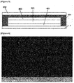
- Figure 1 illustratively shows a plastic substrate (1) having a supporting layer (101) comprising a polymeric binder (1011) and a scattering component (1012) included in the polymeric binder.
- the scattering component (1012) may be completely incorporated in the polymeric binder (1011) and the supporting layer (101) may have a flat surface, a shown in Figure 1 .
- the scattering component (1012) may also be exposed on a surface of the polymeric binder (1011) and the surface of the supporting layer (101) may have a concave-convex structure, as shown in Figure 2 .
- scattering component herein may mean, for example, a material that may have a refractive index different from a surrounding material such as the polymeric binder together with an appropriate size to form a region being capable of scattering, refracting or diffracting the incident light.
- the scattering component can, for example, be in the form of particles.
- a content ratio of the scattering component in the polymeric binder may be properly selected within a range that does not impair objects of the present application.
- the scattering component may be included in a ratio in the range of 0.05% to 3.75% by weight in the polymeric binder.
- the content ratio of the scattering component in the polymeric binder is A% by weight herein may mean that the content ratio of the scattering component relative to 100% by weight of the polymeric binder is A% by weight.
- 100% by weight of the polymeric binder herein may mean a weight ratio based on the weight of the polymeric binder except for the solvent.
- the upper limit of the content ratio of the scattering component in the polymeric binder may be, specifically, 3.75% by weight or less, 3.5% by weight or less, 3.25% by weight or less, 3% by weight or less, 2.75% by weight or less, 2.5% by weight or less, 2.25% by weight or less, 2% by weight or less, 1.9% by weight or less, 1.8% by weight or less, 1.7% by weight or less or 1.6% by weight or less.
- the lower limit of the content ratio of the scattering component in the polymeric binder may be, specifically, 0.05% by weight or more, 0.1 % by weight or more, 0.15% by weight or more, 0.2% by weight or more, 0.25% by weight or more, 0.3% by weight or more, 0.35% by weight or more, 0.4 % or more, 0.45% by weight or more or 0.5% by weight or more.
- the content ratio of the scattering component in the polymeric binder is within the above range, the plastic substrate having excellent light extraction efficiency can be provided.
- the content ratio of the scattering component in the polymeric binder is not necessarily limited to the above range, but may be also adjusted less than or more than the above range in consideration of haze characteristics of the support layer and/or the plastic substrate intended to be embodied.
- the upper limit of the content ratio of the scattering component in the polymeric binder may be appropriately about 10% by weight, considering an aspect that the plastic substrate of the present application is prepared by adding the scattering component to a polymeric binder precursor secondarily, as described below.
- the upper limit of the content ratio of the scattering component in the polymeric binder precursor is greater than about 10% by weight, a phenomenon that a filter is clogged in a step of filtering occurs to make no sufficient filtering, and thus after coating a layer of a composition comprising the polymeric binder precursor and the scattering component the surface of the coating layer is so rough that it may be disadvantageous to manufacture the device.
- a thickness of the supporting layer may be appropriately selected within a range that does not impair objects of the present application.
- the thickness of the supporting layer may be in a range of about 10 ⁇ m to 130 ⁇ m.
- the upper limit of the thickness of the supporting layer may be, specifically, 130 ⁇ m or less, 120 ⁇ m or less, 110 ⁇ m or less, 100 ⁇ m or less, 90 ⁇ m or less, 80 ⁇ m or less, or 70 ⁇ m or less.
- the lower limit of the thickness of the supporting layer may be, specifically, 10 ⁇ m or more, 20 ⁇ m or more, 30 ⁇ m or more, 40 ⁇ m or more, 50 ⁇ m or more or 60 ⁇ m or more.
- the supporting layer itself to have a sufficient thickness so as to be capable of performing a function as a substrate such as an organic electronic device that the thickness of the supporting layer is within the above range.
- this is different from a structure coating a light extraction layer in a very thin thickness, for example, a thickness of about 2 ⁇ m or less on a general plastic substrate (without light extraction efficiency) with a sufficient thickness which may perform a function as a substrate.
- the supporting layer may perform the function as the substrate and the function as the light extraction layer at the same time, and thus it is advantageous in the production side of the substrate.
- the haze of the plastic substrate may be appropriately selected within a range that does not impair objects of the present application.
- the haze of the plastic substrate may be in a range of about 5% to 80%.
- the upper limit of the haze of the plastic substrate may be, specifically, 80% or less, 77.5% or less, 75% or less, 72.5% or less, 70% or less, 67.5% or less, 65% or less, 62.5% or less, 60% or less, 57.5% or less or 55 % or less.
- the lower limit of the haze of the plastic substrate may be, specifically, 5% or more, 7.5% or more, 10% or more, 12.5% or more, 15% or more, 17.5% or more, 20% or more, 22.5% or more, 25% or more, 27.5% or more, 30% or more, 32.5% or more, 35% or more, 37% or more, 40% or more, 42.5% or more, or 45% or more, 47.5% or more, 50% or more or 52.5% or more. If the haze of the plastic substrate is within the above range, the plastic substrate having excellent light extraction efficiency can be provided.
- a method for measuring the haze of the plastic substrate herein is not particularly limited and the haze can be measured by employing a haze measurement method known in the art.
- the haze may be measured using a D65 light source with a haze measuring instrument known in the art (Hazemeter), for example, HM-150 system from MURAKAMI Co., Ltd.
- the plastic substrate may exhibit the haze range even in a state comprising no haze inducing element other than the scattering component of the supporting layer.
- the plastic substrate herein comprises no haze inducing element other than the scattering component of the supporting layer, which may mean that the element inducing the haze in the plastic substrate is only the scattering component and it further comprises no haze inducing layer or further adds no haze inducing component on polymerizing the polymeric binder.
- the plastic substrate of the present application may exhibit a haze in the range from about 5% to 80% in a state that comprises no haze inducing element other than the scattering component of the supporting layer.
- the upper limit of the haze of the plastic substrate may be, specifically, 80% or less, 77.5% or less, 75% or less, 72.5% or less, 70% or less, 67.5% or less, 65% or less, 62.5% or less, 60% or less, 57.5% or less or 55 % or less.
- the lower limit of the haze of the plastic substrate may be, specifically, 5% or more, 7.5% or more, 10% or more, 12.5% or more, 15% or more, 17.5% or more, 20% or more, 22.5% or more, 25% or more, 27.5% or more, 30% or more, 32.5% or more, 35% or more, 37% or more, 40% or more, 42.5% or more, 45% or more, 47.5% or more, 50% or more or 52.5% or more.
- the plastic substrate may be prepared by adding the scattering component secondarily prior to conversion from the polymeric binder precursor to the polymeric binder, thereby securing a stable dispersibility of the scattering component in the polymeric binder, so that it can exhibit excellent haze properties as above, although it comprises no separate haze inducing element other than the scattering component.
- the plastic substrate of the present application has excellent surface roughness characteristics.
- the surface roughness characteristics of the substrate herein are excellent, which may mean that the surface roughness of the substrate is low, so that the surface is flat.
- the supporting layer comprising the polymeric binder and the scattering component
- the higher the content ratio of the scattering component and the thicker the thickness of the supporting layer it is expected that the haze may be increased.
- the content ratio of the scattering component is relatively low and the thickness of the supporting layer is relatively high, but as compared with the case having the relatively high ratio of the scattering component and the relatively low thickness of the supporting layer, the plastic substrate can exhibit more excellent surface roughness characteristics, even if it exhibits similar haze characteristics.
- the plastic substrate of the present application is prepared by adding the scattering component to the polymeric binder precursor, which can secure the dispersibility of the scattering component in the supporting layer stably compared to the last-addition method because a phenomenon that the scattering component agglomerates in the surface of the supporting layer may be reduced. If the phenomenon that the scattering component agglomerates in the surface of the plastic substrate occurs, a short may be caused so as to be disadvantageous in manufacturing devices.
- the plastic substrate of the present application is more advantageous in terms of dispersion stability of the scattering component in the supporting layer, distribution uniformity of the scattering component and surface roughness characteristics, over the prior art coating the light extraction layer in a very thin thickness on the general plastic substrate with a thickness sufficient being capable of performing the function as a substrate.
- the supporting layer may have a surface roughness (Ra) in a range of about 0.1 nm to 30 nm, measured in a region of at least 20 ⁇ m x 20 ⁇ m.
- the upper limit of the surface roughness (Ra) may be more specifically 30 nm or less, 27.5 nm or less, 25 nm or less, 22.5 nm or less, 20 nm or less, 17.5 nm or less, 15 nm or less or 12.5 nm or less.
- the lower limit of the surface roughness (Ra) may be more specifically 0.1 nm or more, 1 nm or less, 2 nm or more, 3 nm or more, 4 nm or more, 5 nm or more, 6 nm or more, 7 nm or more, 8 nm or more or 9 nm or more. If the surface roughness of the supporting layer is within the above range, the plastic substrate can exhibit excellent surface roughness characteristics, and when the plastic substrate is applied to a substrate of an organic electronic device to be described below, it is advantageous in terms of manufacturing organic electronic devices, without causing a problem such as a short.
- a method of measuring the surface roughness herein is not particularly limited and the surface roughness can be measured by employing a surface roughness measuring method known in the art.
- the surface roughness may be measured using AFM (atomic force microscope) equipment known in the art, for example, NS4 D3100 DEN P-4 Rev. A equipment from Digital Instrument Inc. by non-contact (vibrating) method.
- the plastic substrate of the present application also exhibits an excellent translucency.
- the transmittance for light having a wavelength in the visible light range for example, a wavelength of 550 nm or 638 nm may be at least 80%, at least 82%, at least 84%, at least 86%, at least 88% or at least 90%.
- the plastic substrate of the present application comprises a relatively low content of the scattering component and uses a supporting layer of a relatively thick thickness, and thus can exhibit the above excellent translucency. Since the plastic substrate of the present application has the above excellent translucency, it may be suitable as a substrate of a bottom emitting organic electronic device, but is not limited thereto.
- the plastic substrate of the present application may exhibit an excellent durability and resistance to peeling, and the like even in a process of forming organic electronic devices in which a high temperature is required.
- the thermal expansion coefficient of the plastic substrate may be in a range of 10 ppm/°C to 50 ppm/°C, without being limited thereto.
- the plastic substrate of the present application may exhibit a high refractive index.
- the refractive index for light having a wavelength of 550 nm or 633 nm in the plastic substrate may be about 1.5 or more, about 1.6 or more, about 1.65 or more, or about 1.7 or more.
- the upper limit of the refractive index is not particularly limited, but for example, may be 1.9 or less, 1.85 or less, 1.80 or less, 1.75 or less.
- Such a refractive index range can be secured, for example, by forming the plastic substrate with a polymer material having a high refractive index or by blending high refractive index particles in the material of the plastic substrate. If the refractive index of the plastic substrate satisfies the above range, a total reflection phenomenon, and the like may be eliminated or mitigated to embody an organic electronic device having excellent light extraction efficiency.
- the polymeric binder may comprise polyimide, polyethylene naphthalate, polycarbonate, acrylic resin, polyethylene terephthalate, polysulfone, polyether sulfide, polypropylene, polyetherether ketone or polydimethylsiloxane, but is not limited thereto.
- polyimide may be selected as the above polymeric binder and used, in terms of process temperatures or light extraction efficiency.
- Such a polyimide may be prepared by using monomers introducing, for example, a halogen atom, a sulfur atom or a phosphorus atom.
- the polymer binder may include a polyimide compound comprising a repeating unit of Formula 1 below.
- R 1 to R 20 are each independently hydrogen, an alkyl group, an alkoxy group, an aryl group or a functional group comprising a halogen atom, a sulfur atom or a phosphorus atom, and n is an integer of 1 or more.
- substituents of R 1 to R 20 substituted on carbon atoms linking two ring structures from each other are not present. For example, if the carbon atom linked by R 2 and the carbon atom linked by R 8 link benzene rings, R 2 and R 5 are not present.
- single bond herein may mean that no separate atom or atom group is present on the corresponding site.
- benzenes on both sides of -L- may be directly linked to form a biphenyl structure.
- the alkyl group herein may be, for example, a straight or branched alkyl group having 1 to 20 carbon atoms, 1 to 16 carbon atoms, 1 to 12 carbon atoms, 1 to 8 carbon atoms or 1 to 4 carbon atoms, unless particularly specified otherwise.
- the alkyl group may be optionally substituted by one or more substituents.
- the alkoxy group herein may mean an alkoxy group having 1 to 20 carbon atoms, 1 to 16 carbon atoms, 1 to 12 carbon atoms, 1 to 8 carbon atoms or 1 to 4 carbon atoms, unless particularly specified otherwise.
- the alkoxy group may be straight, branched or cyclic.
- the alkoxy group may be optionally substituted by one or more substituents.
- the aryl group or the arylene group herein may mean a monovalent residue or bivalent residue derived from an aromatic compound or a derivative thereof comprising benzene or a structure in which two or more benzenes are fused or bonded while sharing two or one carbon atom, unless particularly specified otherwise.
- the aryl group or the arylene group may be, for example, an aryl group or an arylene group, having 6 to 22 carbon atoms, 6 to 20 carbon atoms, 6 to 18 carbon atoms, 6 to 16 carbon atoms, 6 to 14 carbon atoms or 6 to 12 carbon atoms, and the aryl group or the arylene group may be optionally substituted by one or more substituents.
- the alkylene group or the alkylidene group herein may mean, for example, an alkylene group or an alkylidene group, having 1 to 20 carbon atoms, 1 to 16 carbon atoms, 1 to 12 carbon atoms, 1 to 8 carbon atoms or 1 to 4 carbon atoms, unless particularly specified otherwise.
- the alkylene group or the alkylidene group may be, for example, straight, branched or cyclic.
- the alkylene group or the alkylidene group may be optionally substituted by one or more substituents.
- the alkenylene group or the alkynylidene group herein may mean, for example, an alkenylene group or an alkynylidene group, having 2 to 20 carbon atoms, 2 to 16 carbon atoms, 2 to 12 carbon atoms, 2 to 8 carbon atoms or 2 to 4 carbon atoms, unless particularly specified otherwise.
- the alkenylene group or the alkynylidene group may be, for example, straight, branched or cyclic.
- the alkenylene group or the alkynylidene group may be optionally substituted by one or more substituents.
- the alkenyl group herein may be, for example, an alkenyl group having 2 to 20 carbon atoms, 2 to 16 carbon atoms, 2 to 12 carbon atoms, 2 to 8 carbon atoms or 2 to 4 carbon atoms, unless particularly specified otherwise.
- the alkenyl group may be, for example, straight, branched or cyclic.
- the alkenyl group may be optionally substituted by one or more substituents.
- a substituent which may be substituted on an alkyl group, an alkoxy group, an aryl group, an alkylene group, an alkylidene group, an alkenylene group, an alkynylene group or an arylene group, a functional group comprising a halogen atom such as fluorine, chlorine, bromine or iodine, etc., a sulfur atom or a phosphorus atom, a phenyl group, a benzyl group, a naphthyl group or a thiophenyl group and the like may be exemplified, without being limited thereto.
- the polymeric binder may be a homopolymer formed by only the repeating unit of Formula 1, or a block or random copolymer comprising other units together in addition to the repeating unit of Formula 1.
- both ends of the polymer may be each independently hydrogen, an alkyl group, an alkoxy group, an aryl group or a functional group comprising a halogen atom, a sulfur atom or a phosphorus atom.
- kinds or ratios of other repeating units may be suitably selected, for example, from a range that does not inhibit the desired refractive index, heat resistance, or translucency and the like.
- the polymeric binder comprising the repeating unit of Formula 1 above may have, for example, a weight average molecular weight in terms of standard polystyrene of 10,000 to 100,000 or about 10,000 to 50,000 or so, measured by GPC (Gel Permeation Chromatograph).
- the polymeric binder having the repeating unit of Formula 1 has also a light transmittance of at least 80%, at least 85% or at least 90% in a visible light range and an excellent heat resistance.
- an average particle diameter of the scattering component may be in a range of 150 nm to 300 nm.
- the lower limit of the average particle diameter of the scattering component may be specifically 150 nm or more, 160 nm or more, 170 nm or more, 180 nm or more, 190 nm or more or 200 nm or more.
- the upper limit of the average particle diameter of the scattering component may be specifically 300 nm or less, 290 nm or less, 280 nm or less, 270 nm or less, 260 nm or less or 250 nm or less. If the average particle diameter of the scattering component satisfies the above range, the plastic substrate having excellent light extraction efficiency can be provided.
- the scattering component may have higher or lower refractive index relative to surrounding materials, for instance, the polymeric binder.
- an absolute value of a difference in refractive indices of the polymeric binder and the scattering component for light having a wavelength of 550 nm or 633 nm may be in a range of 0.5 to 1.2.
- the lower limit of the absolute value of the difference in the refractive indices may be specifically 0.5 or more, 0.55 or more, 0.6 or more, 0.65 or more or 0.7 or more.
- the upper limit of the absolute value of the difference in the refractive indices may be specifically 1.2 or less, 1.15 or less, 1.1 or less, 1.05 or less, or 1 or less.
- the organic electronic device having excellent light extraction efficiency can be provided by suitably scattering, refracting or diffracting light incident on the plastic substrate.
- the shape of the scattering component may be appropriately selected within a range that does not impair objects of the present application.
- the scattering component may have a shape such as a sphere, an ellipsoid, a polyhedron or an amorphous shape, without being limited thereto.
- the known materials may be appropriately selected and used, which are known in the art as materials being capable of forming regions that can scatter, refract or diffract the incident light in a state contained in the polymeric binder.
- the scattering component may comprise, for example, an organic material and/or an inorganic material.
- organic material for example, organic materials comprising one or more selected from the group consisting of acrylic resin, styrene resin, olefin resin, nylon resin, melamine resin, formaldehyde resin, silicone resin, urethane resin, polyester resin, polycarbonate resin, and derivatives thereof may be exemplified, but is not limited thereto.
- a metal or a metal oxide may be exemplified, but is not limited thereto.
- inorganic materials comprising one or more selected from the group consisting of TiO 2 , HfO 2 , BaTiO 3 , SnO 2 , ZrO 2 , ZnO, Al 2 O 3 and SiO 2 may be exemplified, but is not limited thereto.
- the scattering component may be formed by including any one material only or at least two materials of the above materials.
- hollow particles such as hollow silica or particles of core/shell structure may be also used as the scattering component.
- An exemplary plastic substrate of the present application may further have a barrier layer formed on one side or both sides of the support layer.
- barrier layer herein may mean a layer having a function for preventing penetration of oxygen, water, nitrogen oxide, sulfur oxide, or ozone in the air.
- the barrier layer has the above function, it is not particularly limited and may be suitably selected according to the intended use.
- the barrier layer may be formed on one or both sides of the plastic substrate via a buffer layer. That is, the plastic substrate may further comprise the buffer layer formed between the barrier layer and the supporting layer.
- the buffer layer may serve to improve adhesion between the barrier layer and the substrate layer.
- the buffer layer may be formed by depositing an inorganic layer such as, for example, SiO 2 , SiONx or SiNx with a sputtering method or the known vacuum vapor deposition method. If necessary, the buffer layer may be formed by a method with an organic material/ inorganic material coating.
- a material of the barrier layer a material having a function to prevent substances which promote degradation of devices, such as moisture and oxygen, from entering into the device may be selected without limitation and used.
- the barrier layer may include a metal such as In, Sn, Pb, Au, Cu, Ag, Al, Ti and Ni; a metal oxide such as TiO, TiO 2 , Ti 3 O 3 , Al 2 O 3 , MgO, SiO, SiO 2 , GeO, NiO, CaO, BaO, Fe 2 O 3 , Y2O 3 , ZrO 2 Nb 2 O 3 and CeO 2 ; a metal nitride such as SiN; a metal oxynitride such as SiON; a metal fluoride such as MgF 2 , LiF, AlF 3 and CaF 2 ; polyethylene, polypropylene, polymethyl methacrylate, polyimide, polyurea, polytetrafluoroethylene, polychlorotrifluoroethylene, polydichlorodifluoroethylene, or a copolymer of chlorotrifluoroethylene and dichlorodifluoroethylene; a copolymer obtained by copo
- the material of the barrier layer may be a metal oxide.
- the material of the barrier layer may be a metal oxide of high refractive index.
- the refractive index of the barrier layer may be, for example, 1.45 or more, about 1.5 or more, about 1.6 or more, about 1.65 or more or about 1.7 or more for a wavelength of 633 nm.
- the upper limit of the refractive index of the barrier layer can be adjusted appropriately according to the desired function, and for example, the refractive index for a wavelength of 633 nm may be 2.6 or less, 2.3 or less, 2.0 or less or 1.8 or less. If the refractive index of the barrier layer satisfies the above range, the total reflection phenomenon may be eliminated or mitigated to embody an organic electronic device having excellent light extraction efficiency.
- the barrier layer may be either a single layer structure or a multi-layer structure.
- the single layer structure may include one material of the barrier layer or at least two materials of the barrier layer as a mixture.
- the multi-layer structure may be, for example, a structure that two or more layers of the single layer structure are laminated, and in one suitable example, the barrier layer may be the multi-layer structure that a titanium oxide layer (for example, TiO 2 layer) and an aluminum oxide layer (for example, Al 2 O 3 layer) are sequentially laminated.
- the thickness of the barrier layer is not particularly limited and can be suitably selected according to the intended use.
- the thickness of the barrier layer may be 5 nm to 1000 nm, 7 nm to 750 nm or 10 nm to 500 nm.
- the light transmittance of the barrier layer is not particularly limited and may be suitably selected according to the intended use.
- the light transmittance of the barrier layer may be at least about 80%, at least 85% or at least 90%.
- the barrier layer may have a refractive index equal to that of the adjacent layer.
- the barrier layer when an electrode layer is adjacent to the barrier layer, the barrier layer may have a refractive index of 1.5 or more for light having a wavelength of 550 nm or 633 nm. Accordingly, the total reflection phenomenon at the interface between the barrier layer and the electrode layer may be eliminated or mitigated to embody an organic electronic device having excellent light extraction efficiency.
- the barrier layer may have a water vapor transmission rate (WVTR) of 10 -4 g/m 2 ⁇ day or less.
- the water vapor transmission rate may be, for example, a value measured in a condition that a temperature is 40°C and a relative humidity is 90%.
- the water vapor transmission rate may be measured using, for example, a water vapor transmission rate measuring instrument (PERMATRAN-W3/31, manufactured by MOCON, Inc.).
- the barrier layer may be a layer formed by, for example, an ALD (Atomic Layer Deposition) method, a vacuum deposition method, a sputtering method, a reactive sputtering method, an MBE (molecular beam epitaxy) method, a cluster ion beam method, an ion plating method, a plasma polymerization method (high frequency excited ion plating method), a plasma CVD method, a laser CVD method, a thermal CVD method, a gas source CVD method or a coating method, and in one suitable example, it may be an atomic layer deposition formed by the ALD method.
- ALD Atomic Layer Deposition
- the plastic substrate of the present application may further comprise a plane layer.
- the plane layer may be formed, for example, on one or both sides of the supporting layer.
- the plane layer may be formed on top of the supporting layer surface with such a uneven structure.
- Figure 3 illustratively shows a plastic substrate (1) having a structure that a plane layer (301) is formed on top of the supporting layer (101) having a surface of concave-convex structure.
- the plane layer may comprise, for example, high refractive particles together with a binder.
- the plane layer may be formed using a composition in which high refractive particles are mixed with the binder.
- the plane layer may provide a surface that can form an organic electronic device including an electrode layer, etc., and have a light scattering property to improve light extraction efficiency of the device.
- the plane layer may have a refractive index equal to or more than that of the adjacent electrode layer, for example, a refractive index of 1.5 or more for light having a wavelength of 550 nm or 633 nm.
- the known materials can be used without particular limitation.
- various organic binders, inorganic binders or organic and inorganic binders, known in the art may be used.
- Organic binders, inorganic binders or organic and inorganic binders, having excellent heat resistance and chemical resistance, may be selected and used, considering a lifetime of the device or excellent resistance against a high temperature process, a photo process or an etching process to be performed in the manufacturing processes.
- the binder may have a refractive index of, for example, about 1.4 or more, about 1.45 or more, about 1.5 or more, about 1.6 or more, about 1.65 or more or about 1.7 or more.
- the upper limit of the refractive index of the binder may be selected from a range that can satisfy the refractive index of the plane layer, in consideration of the refractive index of the particles to be compounded together.
- the binder for example, epoxy resin, polysiloxane or polyimide may be exemplified.
- high refractive binders or low refractive binders may be used as the binder of the plane layer.
- the term "high refractive binder” herein may mean a binder having a refractive index of about 1.7 to 2.5 or about 1.7 to 2.0 and the term “low refractive binder” may mean a binder having a refractive index from about 1.4 or more to less than 1.7.
- Such binders have been variously known, and a suitable binder among various kinds of binders as described above or other known binders may be selected and used.
- the plane layer may further comprise high refractive particles.
- high refractive particles in the plane layer may be, for example, particles having a refractive index of 1.8 or more, 2.0 or more, 2.2 or more, 2.5 or more, 2.6 or more or 2.7 or more.
- the upper limit of the refractive index of the high refractive particles may be selected from a range that can satisfy the refractive index of the plane layer, in consideration of the refractive index of the binder and the like to be compounded together.
- the high refractive particles may have an average particle diameter of, for example, 1 nm to 100 nm, 10 nm to 90 nm, 10 nm to 80 nm, 10 nm to 70 nm, 10 nm to 60 nm, 10 nm to 50 nm or 10 nm to 45 nm or so.
- the high refractive particles for example, alumina, aluminosilicate, titanium oxide or zirconium oxide, and the like may be exemplified.
- rutile type titanium oxide may be used.
- Titanium oxide of the rutile type has a higher refractive index than that of the other particles, and thus it may be possible to adjust the desired refractive index even in a relatively low ratio.
- the refractive index of the high refractive particles may be a refractive index measured for light having a wavelength of 550 nm or 633 nm.
- the plane layer may comprise high refractive particles having a refractive index of 1.8 or more for light having a wavelength of 633nm and an average particle diameter of 50 nm or less.
- the ratio of the high refractive particles in the plane layer is not particularly limited, and may be adjusted within a range in which the refractive index of the above-described plane layer can be secured.
- the high refractive particles may be included in the plane layer in a ratio of 300 parts by weight or less, 250 parts by weight or less, 200 parts by weight or less, 150 parts by weight or less or 120 parts by weight or less relative to 100 parts by weight of the binder.
- the ratio of the high refractive particles may be, for example, 40 parts by weight or more, 60 parts by weight or more, 80 parts by weight or more, or 100 parts by weight or more.
- the "unit of part by weight” herein means the ratio of weight between the components, unless particularly specified otherwise.
- the device having excellent performance and reliability can be provided by increasing the external quantum efficiency, preventing gas and moisture outside from permeating, and reducing the outgassing.
- the plane layer may be formed through, for example, a wet coating method using a coating liquid comprising a binder and high refractive particles, a sol-gel method or a deposition method such as CVD (Chemical Vapor Deposition) or PVD (Physical Vapor Deposition) methods or a micro-embossing method, without being limited thereto.
- a wet coating method using a coating liquid comprising a binder and high refractive particles a sol-gel method or a deposition method such as CVD (Chemical Vapor Deposition) or PVD (Physical Vapor Deposition) methods or a micro-embossing method, without being limited thereto.
- CVD Chemical Vapor Deposition
- PVD Physical Vapor Deposition
- the plane layer may be also formed using a material that a compound such as alkoxide or acylate of a metal, for example, zirconium, titanium or cerium, is compounded with a binder having a polar group such as a carboxyl group or a hydroxyl group.
- a compound such as alkoxide or acylate may be subjected to condensation with the polar group present in the binder, which includes the metal in the backbone of the binder, to embody high refractive index.
- titanium alkoxides such as tetra-n-butoxy titanium, tetraisopropoxy titanium, tetra-n-propoxy titanium or tetraethoxy titanium
- titanium acylates such as titanium stearate, titanium chelates, zirconium alkoxides such as tetra-n-butoxy zirconium, tetra-n-propoxy zirconium, tetraisopropoxy zirconium or tetraethoxy zirconium
- zirconium acylates such as zirconium tributoxystearate, zirconium chelates and the like may be exemplified.
- the plane layer may be also formed by a sol-gel coating process that a metal alkoxide such as titanium alkoxide or zirconium alkoxide and a solvent such as alcohol or water are compounded to prepare a coating liquid, which is applied and then baked at an appropriate temperature.
- a metal alkoxide such as titanium alkoxide or zirconium alkoxide
- a solvent such as alcohol or water
- the plastic substrate of the present application may further comprise a carrier substrate which is attached to one surface of the supporting layer.
- the barrier layer or the plane layer when the barrier layer or the plane layer is further formed on the plastic substrate, the surface opposite the barrier layer or the plane layer may be in contact with the carrier substrate.
- the carrier substrate may be, for example, a glass substrate or a rigid substrate.
- the glass substrate an appropriate material may be used, without particular limitations, and for example, a base material layer such as soda lime glass, barium/strontium-containing glass, lead glass, aluminosilicate glass, borosilicate glass, barium borosilicate glass or quartz may be exemplified, without being limited thereto.
- the carrier substrate may be formed to be detachable with the plastic substrate and included.
- An exemplary method for producing the plastic substrate of the present application comprises forming a layer of a composition comprising a polymeric binder precursor and a scattering component and converting the polymeric binder precursor to the polymeric binder in said layer.
- the composition comprising a polymeric binder precursor and a scattering component may comprise the scattering component in a ratio within a range of about 0.05% by weight to 3.75% by weight relative to 100% by weight of the polymeric binder precursor.
- "100% by weight of polymer binder precursor” herein may mean a weight ratio based on the weight of the polymeric binder precursor, excluding the solvent.
- the details on the content ratio of the scattering component in the polymeric binder described in the section of the plastic substrate can be same applied.
- the layer of the composition may be formed to have a thickness in a range of about 10 ⁇ m to 130 ⁇ m.
- the layer of the composition may become the supporting layer described in the section of the plastic substrate by converting the polymeric binder precursor to the polymeric binder. Therefore, for specific details on the thickness of the layer of the composition, the details on the thickness of the supporting layer described in the section of the plastic substrate can be same applied.
- the above method relates to the method for producing the plastic substrate, in the above method, even for the details other than the content ratio of the scattering component and the thickness of the layer of the composition, the details described in the section of the plastic substrate can be same applied. Therefore, in the case of producing a plastic substrate by the above method, the plastic substrate exhibiting the haze characteristics described in the section of the plastic substrate can be produced.
- the above method prepares the plastic substrate by adding the scattering component secondarily.
- second-addition herein may mean that in the method for producing the plastic substrate having the supporting layer comprising the polymeric binder and the scattering component, a process of adding the scattering component is performed before the polymeric binder precursor is converted to the polymeric binder. That is, the term “second-addition” herein may mean that in the method for producing the plastic substrate, the scattering component is added to the polymeric binder precursor.
- the term “last-addition” herein may mean that in the method for producing the plastic substrate, the process of adding the scattering component is performed after the polymeric binder precursor is converted to the polymeric binder. That is, the term “last-addition” herein may mean that in the method for producing the plastic substrate, the scattering component is added to the polymer binder.
- polymeric binder precursor may mean a material which is an ingredient needed to form the polymeric binder or a precursor material of the polymeric binder in a series of reactions forming the polymeric binder.
- the polymeric binder precursor can be appropriately selected according to the type of the polymeric binder.
- the polymeric binder is polyimide
- the polymeric binder precursor may mean polyamic acid or a monomeric compound for synthesizing polyamic acid.
- the scattering component is compounded to the polyamic acid or the monomeric compound for synthesizing the polyamic acid, the above method can be said to have been added secondarily.
- the scattering component When the scattering component is added secondarily to prepare the plastic substrate as the above method, the stable dispersibility of the scattering component in the polymeric binder precursor and/or the polymeric binder can be secured and thus the plastic substrate having excellent surface roughness characteristics with exhibiting the haze suitable to the light extraction efficiency can be prepared.
- the dispersibility of the scattering component in the polymeric binder cannot be secured and thus the aggregation phenomenon of the scattering component can be caused inside the polymeric binder or on the surface of the layer of the composition, thereby it is difficult to exhibit the haze suitable to light extraction efficiency and the surface roughness characteristics are lowered, so that there is a disadvantage on preparing the device.
- the composition may be prepared by dissolving the polymeric binder precursor and the scattering component in a suitable solvent.
- a suitable solvent it is possible to use the known organic solvent such as toluene, xylene, cyclopentanone or cyclohexanone.
- the composition may further comprise an additive such as a polymerization initiator and a surfactant.
- the layer of the composition can be formed by applying a composition comprising a polymer binder precursor and a scattering component on a suitable substrate.
- the substrate can be a carrier substrate described in the section of the plastic substrate.
- the application method is not particularly limited and the known coating method may be applied.
- a method such as roll coating, printing method, inkjet coating, slit nozzle method, bar coating, comma coating, spin coating or gravure coating, can be exemplified.
- the polymeric binder precursor may be polyamic acid.
- the polyamic acid the known polyamic acid being capable of forming polyimide may be used.
- the polyamic acid including a repeating unit represented by Formula 2 below may be used as the polyamic acid.
- R 1 to R 20 are each independently hydrogen, an alkyl group, an alkoxy group, an aryl group or a functional group containing a halogen atom, a sulfur atom or a phosphorus atom, and n is an integer of 1 or more.
- R 1 to R 20 substituted on carbon atoms linking two ring structures from each other are not present.
- R 2 and R 8 are linked, R 2 and R 8 are absent, and if - NH- group and the carbon atom linked by R 14 are linked, R 14 is absent.
- the process for converting the polymeric binder precursor to the polymeric binder in the layer of the composition may be carried out by a process for being subjected to imidization of polyamic acid.
- Conditions and manners of the imidization are not particularly limited and the conditions and manners of the imidization converting polyamic acid to polyimide known in the art may be applied.
- the present application also relates to a use of the plastic substrate.
- the present application relates to an organic electronic device comprising the plastic substrate.
- the organic electronic device may comprise a plastic substrate having a supporting layer, which comprises a polymeric binder and a scattering component contained in a ratio within a range of 0.05% by weight to 3.75% by weight in the polymeric binder and has a thickness in a range of 10 ⁇ m to 130 ⁇ m, and having a haze in a range of 5% to 80%; a first electrode layer formed on the substrate; an organic layer formed on the first electrode layer and a second electrode layer formed on the organic layer.
- the details described in the section of the plastic substrate can be same applied.
- the organic layer may comprise at least a light emitting layer.
- a bottom emitting device that the light generated in the light emitting layer of the organic layer is emitted via an optically functional layer toward the base material layer may be embodied.
- the organic electronic device may be an organic light emitting device.
- the organic electronic device may have a structure the organic layer comprising at least the light emitting layer is interposed between a hole-injection electrode layer and an electron-injection electrode layer.
- the first electrode layer formed on the plastic substrate may be a hole-injection electrode layer
- the second electrode layer formed on the organic layer may be an electron-injection electrode layer.
- the first electrode layer may be a transparent electrode layer.
- the organic layer existing between the electron and hole injection electrode layers may comprise at least one or more layers of the light emitting layer.
- the organic layer may also comprise two or more layers of a plurality of light-emitting layers. If two or more layers of the light emitting layer are included, the light emitting layers may also have a structure divided by an intermediate electrode layer or a charge generating layer (CGL), having a charge generating property.
- CGL charge generating layer
- the light emitting layer may be formed using, for example, various fluorescent or phosphorescent organic materials known in the art.
- materials of the light emitting layer materials of Alq series such as tris(4-methyl-8-quinolinolate) aluminum (III) (Alg3), 4-MAlq3 or Gaq3, cyclopenadiene derivatives such as C-545T (C 26 H 26 N 2 O 2 S), DSA-amine, TBSA, BTP, PAP-NPA, spiro-FPA, Ph 3 Si (PhTDAOXD), PPCP (1,2,3,4,5-pentaphenyl-1,3-cyclopentadiene), DPVBi (4,4'-bis(2,2'-diphenylvinyl)-1,1'-biphenyl), distyryl benzene or a derivative thereof, or phosphorescent materials such as DCJTB (4-(dicyanomethylene)-2-tert-butyl-6-(1,1,7,7,-tetramethyl
- the light emitting layer may also have a host-dopant system, which comprises the above materials as a host and also perylene, distyrylbiphenyl, DPT, quinacridone, rubrene, BTX, ABTX or DCJTB, etc. as a dopant.
- a host-dopant system which comprises the above materials as a host and also perylene, distyrylbiphenyl, DPT, quinacridone, rubrene, BTX, ABTX or DCJTB, etc.
- the light emitting layer can also be formed by suitably employing a type showing light-emitting characteristics among electron-accepting organic compounds or electron-donating organic compounds as described below.
- the organic layer comprises the light emitting layer, it can be formed in various structures further comprising other various functional layers known in the art.
- a layer that can be included in the organic layer an electron injection layer, a hole blocking layer, an electron transport layer, a hole transport layer and a hole injection layer and the like can be exemplified.
- the electron injection layer or the electron transport layer can be formed, for example, by using the electron-accepting organic compound.
- the electron-accepting organic compound any known compound may be used without particular limitation.
- an organic compound polycyclic compounds or derivatives thereof, such as p-terphenyl or quaterphenyl, polycyclic hydrocarbon compounds or derivatives thereof, such as naphthalene, tetracene, pyrene, coronene, chrysene, anthracene, diphenylanthracene, naphthacene or phenanthrene, heterocyclic compounds or derivatives thereof, such as phenanthroline, bathophenanthroline, phenanthridine, acridine, quinoline, quinoxaline or phenazine can be illustrated.
- fluoroceine perylene, phthaloperylene, naphthaloperylene, perynone, phthaloperynone, naphthaloperyn
- fluorescent brighteners such as benzooxazole compound, benzothiazole compounds or benzoimidazole compounds
- distyrylbenzene compounds such as 1,4-bis(2-methylstyryl)benzene, 1,4-bis(3-methylstyryl)benzene, 1,4-bis(4-methylstyryl)benzene, distyrylbenzene, 1,4-bis(2-ethylstyryl)benzyl, 1,4-bis(3-ethylstyryl)benzene, 1,4-bis(2-methylstyryl)-2-methylbenzene or 1,4-bis(2-methylstyryl)-2-ethylbenzene; distyrylpyrazine compounds such as 2,5-bis(4-methylstyryl)pyrazine, 2,5-bis(4-ethylstyryl)pyrazine, 2,5-bis[2-(1-naphthyl)vinyl
- organic tri-functional compounds disclosed in Japanese Unexamined Patent Publication No. 1991-296595 and the like, coumarin derivatives disclosed in Japanese Unexamined Patent Publication No. 1990-191694 and the like, perylene derivatives disclosed in Japanese Unexamined Patent Publication No. 1990-196885 and the like, naphthalene derivatives disclosed in Japanese Unexamined Patent Publication No. 1990-255789 and the like, phthaloperynone derivatives disclosed in Japanese Unexamined Patent Publication No. 1990-289676 or Japanese Unexamined Patent Publication No. 1990-88689 and the like or styrylamine derivatives disclosed in Japanese Unexamined Patent Publication No. 1990-250292 and the like can be also used as the electron-accepting organic compound contained in the low refractive layer.
- the electron injection layer above may be formed, for example, using a material such as LiF or CsF.
- the hole blocking layer is a layer that may prevent the injected holes from passing through the light emitting layer and entering into the electron-injection electrode layer to improve the lifetime and efficiency of the device, and may be formed in an appropriate portion between the emitting layer and the electron-injection electrode layer by using the known material, if necessary.
- the hole injection layer or the hole transport layer can comprise, for example, an electron-donating organic compound.
- an electron-donating organic compound aryl amine compounds, such as N,N,N',N'-tetraphenyl-4,4'-diaminophenyl, N,N'-diphenyl-N,N'-di(3-methylphenyl)-4,4'-diaminobiphenyl, 2,2-bis(4-di-p-tolylamino)propane, N,N,N',N'-tetra-p-tolyl-4,4'-diaminobiphenyl, bis(4-di-p-tolylaminophenyl)phenylmethane, N,N'-diphenyl-N,N'-di(4-methoxyphenyl)-4,4'-diaminobiphenyl, N,N,N',N'-tetraphenyl-4,4'-diamino
- the hole injection layer or the hole transport layer may be also formed by dispersing an organic compound in a polymer or using a polymer derived from the organic compound.
- so-called ⁇ - conjugated polymers such as polyparaphenylenevinylene and its derivatives
- hole-transporting non-conjugated polymers such as poly(N-vinylcarbazole) or ⁇ -conjugated polymers of polysilane can be also used.
- the hole injection layer may be formed by using electrically conductive polymers such as metal phthalocyanine, for example copper phthalocyanine, or non-metal phthalocyanine, a carbon film and polyaniline or may be also formed by reacting the aryl amine compound as an oxidizing agent with a Lewis acid.
- electrically conductive polymers such as metal phthalocyanine, for example copper phthalocyanine, or non-metal phthalocyanine, a carbon film and polyaniline or may be also formed by reacting the aryl amine compound as an oxidizing agent with a Lewis acid.
- the organic light emitting device may have (1) a form of hole injection electrode layer/organic emitting layer/electron injection electrode layer; (2) a form of hole injection electrode layer/hole injection layer/organic light emitting layer/electron injection electrode layer; (3) a form of hole injection electrode layer/organic emitting layer/electron injection layer/electron injection electrode layer; (4) a form of hole injection electrode layer/hole injection layer/organic light emitting layer/electron injection layer/electron injection electrode layer;(5) a form of hole injection electrode layer/organic semiconductor layer/organic emitting layer/electron injection electrode layer; (6) a form of hole injection electrode layer/organic semiconductor layer/electron barrier layer/organic emitting layer/electron injection electrode layer; (7) a form of hole injection electrode layer/organic semiconductor layer/organic emitting layer/adhesion improving layer/electron injection electrode layer; (8) a form of hole injection electrode layer/hole injection layer/hole transport layer/organic emitting layer/electron
- the hole or electron injection electrode layer and the organic layer for example, the light emitting layer, the electron injection or transport layer, the hole injection or transport layer, and methods for forming the same are known, and all the above methods may be applied to production of the above organic electronic devices.
- the organic electronic device may further comprise a sealing structure.
- the sealing structure may be a protective structure that foreign materials such as moisture or oxygen do not flow into the organic layer of the organic electronic device.
- the sealing structure may be, for example, a can such as a glass can or a metal can, or a film covering the entire surface of the organic layer.
- Figure 4 illustratively show a form that the first electrode layer (401), the organic layer (402) and the second electrode layer (403) sequentially formed on the plastic substrate (1) are protected by the sealing structure (404) of a can structure such as a glass can or a metal can.
- the sealing structure (404) may be attached to the plastic substrate (1) by, for example, an adhesive. In such a manner, it is possible to maximize the protection effect through the sealing structure.
- the sealing structure may be, for example, a film covering the entire surface of the first electrode layer, the organic layer and the second electrode layer.
- Figure 5 illustratively shows the sealing structure (501) in a film form covering the entire surface of the first electrode layer (401), the organic layer (402) and the second electrode layer (403).
- the sealing structure (501) in a film form may have a structure that the plastic substrate (1) and the second substrate (502) are adhered to each other, while covering the entire surface of the first electrode layer (401), the organic layer (402) and the second electrode layer (403), as shown in Figure 5 .
- the second substrate for example, a glass substrate, a metal substrate, a polymer film or a barrier layer and the like may be exemplified.
- the sealing structure in a film form may be formed, for example, by applying a liquid material to be cured by heat or irradiation of ultraviolet (UV), such as an epoxy resin, and curing it, or may be formed by a manner that the substrate and the top substrate are laminated using an adhesive sheet and the like prepared ahead in a film form with the epoxy resin and the like.
- UV ultraviolet
- the sealing structure may comprise metal oxides such as calcium oxide, beryllium oxide, metal halides such as calcium chloride or water adsorbents or getter materials such as phosphorus pentoxide and the like, if necessary.
- the water adsorbents or getter materials may be included inside the sealing structure in a film form, or may be present at a predetermined position of the sealing structure of the can structure.
- the sealing structure may further comprise a barrier film or a conductive film, and the like.
- the present application relates also to a use of the organic electronic device, for example, the organic light emitting device.
- the present application relates to a display light source comprising the organic electronic device.
- the present application relates to a lighting apparatus comprising the organic electronic device.
- the display light source backlights of liquid crystal displays (LCD), lightings, light sources of various sensors, printers, copying machines, etc., dash light sources for vehicles, light sources of traffic lights, indicator lights, display devices, plane light emitters, displays, decorations or various lights and the like may be exemplified.
- LCD liquid crystal displays
- organic electronic device when the organic electronic device is applied to the display light source or the illumination device or other uses, other components composing of the display light source or the illumination device or the configuration methods thereof are not particularly limited, and as long as the organic electronic device is applied, any material or method known in the art all can be employed.
- the plastic substrate of the present application has excellent light extraction efficiency and surface roughness characteristics.
- the method for producing the plastic substrate of the present application can prepare the plastic substrate through the process of adding the scattering component secondarily.
- the plastic substrate of the present application can be used as a substrate of the organic electronic device, and the organic electronic device may be used as a display light source and a lighting apparatus.
- the haze of the plastic substrate was measured using a D65 light source by HM-150 system from MURAKAMI Co., Ltd.
- the surface roughness of the plastic substrate was measured using AFM (atomic force microscope) equipment, for example, NS4 D3100 DEN P-4 Rev. A equipment from Digital Instrument Inc. by non-contact (vibrating) method.
- AFM atomic force microscope
- the absolute quantum efficiency of the organic light emitting device was measured by an integrating hemisphere device from OTSUKA Company.
- a plastic substrate having a supporting layer was prepared by using a glass substrate as a carrier substrate.
- the coating liquid was coated on the glass substrate in a range that the finally prepared supporting layer could have a thickness of about 30 ⁇ m and then subjected to imidization to prepare the plastic substrate, in which the refractive index for light having a wavelength of 633 nm is about 1.6, having the supporting layer that the scattering component is dispersed in polyimide.
- the transmittance of the manufactured plastic substrate was about 88%, and the haze was about 5%.
- a hole injection electrode layer comprising ITO (Indium Tin Oxide) was formed on the prepared plastic substrate by the known sputtering method. Continuously, a hole injection layer, a hole transport layer, a light emitting layer, an electron transport layer, an electron injection layer and an electron injection electrode layer were formed using the know materials and methods. Then the above structure was sealed with a glass can to prepare an organic electronic device.
- ITO Indium Tin Oxide
- the transmittance of the manufactured plastic substrate was about 84%, and the haze was about 26%.
- the transmittance of the manufactured plastic substrate was about 81%, and the haze was about 32%.
- Figure 7 (a) and Figure 8 (a) show optical microscopic surface images (dark field mode) and SEM surface images of the prepared plastic substrate, respectively.
- the plastic substrate and the organic electronic device were prepared by performing the same method as Example 1 except that in preparing the plastic substrate, it was changed to include no scattering particle in the polymeric liquid of polyamic acid.
- the transmittance of the manufactured plastic substrate was about 94%, and the haze was about 1%.
- the transmittance of the manufactured plastic substrate was about 78%, and the haze was about 65%.
- the transmittance of the manufactured plastic substrate was about 72%, and the haze was about 84%.
- Comparative Example 4 was prepared in such a way that the content ratio of the scattering component was higher than Example 3, but the scattering component was added lastly after completing polymerization of polyamic acid, whereby the aggregation phenomenon of the scattering component did not secure the stable dispersibility in the polymide, and thus the locally high haze was expressed. As a result of measuring the haze, Comparative Example 4 did not exhibit haze characteristics suitable to the light extraction efficiency, and it was confirmed to locally show about 50% or more of haze.
- Figure 7 (b) and Figure 8 (b) show optical microscopic surface images (dark field mode) and SEM surface images of the prepared plastic substrate, respectively.
- Figure 7 (c) and Figure 8 (c) show optical microscopic surface images (dark field mode) and SEM surface images of the prepared plastic substrate, respectively.
Landscapes
- Chemical & Material Sciences (AREA)
- Organic Chemistry (AREA)
- Health & Medical Sciences (AREA)
- Chemical Kinetics & Catalysis (AREA)
- Medicinal Chemistry (AREA)
- Polymers & Plastics (AREA)
- Engineering & Computer Science (AREA)
- Manufacturing & Machinery (AREA)
- Materials Engineering (AREA)
- Physics & Mathematics (AREA)
- Optics & Photonics (AREA)
- Electroluminescent Light Sources (AREA)
- Laminated Bodies (AREA)
Applications Claiming Priority (2)
| Application Number | Priority Date | Filing Date | Title |
|---|---|---|---|
| KR20140112911 | 2014-08-28 | ||
| PCT/KR2015/009064 WO2016032281A1 (fr) | 2014-08-28 | 2015-08-28 | Substrat en plastique |
Publications (3)
| Publication Number | Publication Date |
|---|---|
| EP3147311A1 true EP3147311A1 (fr) | 2017-03-29 |
| EP3147311A4 EP3147311A4 (fr) | 2018-03-14 |
| EP3147311B1 EP3147311B1 (fr) | 2020-05-27 |
Family
ID=55537001
Family Applications (1)
| Application Number | Title | Priority Date | Filing Date |
|---|---|---|---|
| EP15835521.4A Active EP3147311B1 (fr) | 2014-08-28 | 2015-08-28 | Substrat en plastique |
Country Status (4)
| Country | Link |
|---|---|
| US (1) | US10109818B2 (fr) |
| EP (1) | EP3147311B1 (fr) |
| KR (1) | KR101788923B1 (fr) |
| CN (1) | CN106574059B (fr) |
Families Citing this family (5)
| Publication number | Priority date | Publication date | Assignee | Title |
|---|---|---|---|---|
| WO2017187363A1 (fr) * | 2016-04-29 | 2017-11-02 | Sabic Global Technologies B.V. | Procédé de fabrication d'un substrat oled poreux pour extraction |
| CN107565052B (zh) * | 2017-08-25 | 2020-04-17 | 京东方科技集团股份有限公司 | 封装结构及其制造方法、显示装置 |
| KR102418724B1 (ko) * | 2017-12-05 | 2022-07-08 | 삼성디스플레이 주식회사 | 표시 장치 및 그 제조방법 |
| US11224138B2 (en) | 2018-09-11 | 2022-01-11 | Apple Inc. | Electronic device coatings with ultraviolet light stability |
| US11251406B2 (en) | 2019-03-07 | 2022-02-15 | Vitro Flat Glass Llc | Borosilicate light extraction region |
Family Cites Families (12)
| Publication number | Priority date | Publication date | Assignee | Title |
|---|---|---|---|---|
| JP2894257B2 (ja) | 1994-10-24 | 1999-05-24 | 富士ゼロックス株式会社 | 新規電荷輸送性ポリマー、その製造法およびそれを用いた有機電子デバイス |
| KR20100063729A (ko) | 2007-08-27 | 2010-06-11 | 파나소닉 전공 주식회사 | 유기 이엘 소자 |
| WO2011152275A1 (fr) | 2010-06-02 | 2011-12-08 | 株式会社 きもと | Film à diffusion pour el organique, et dispositif électroluminescent el organique équipé dudit film |
| US9193850B2 (en) * | 2011-08-11 | 2015-11-24 | Samsung Electronics Co., Ltd. | Nanocomposite, process for preparing the same, and surface emitting device |
| KR101871803B1 (ko) | 2011-09-06 | 2018-06-29 | 한국전자통신연구원 | 유기발광다이오드 및 그의 제조방법 |
| TWI512066B (zh) * | 2012-01-16 | 2015-12-11 | Toyo Ink Sc Holdings Co Ltd | 光散射層用樹脂組成物、光散射層、及有機電致發光裝置 |
| KR101352561B1 (ko) | 2012-01-18 | 2014-01-17 | 한국전자통신연구원 | 고분자 물질, 광학 필름 및 유기 발광 소자 |
| KR20130111154A (ko) | 2012-03-30 | 2013-10-10 | 주식회사 엘지화학 | 유기전자소자용 기판 |
| JP6241797B2 (ja) | 2012-07-31 | 2017-12-06 | エルジー・ケム・リミテッド | 有機電子素子用基板 |
| KR101587329B1 (ko) | 2012-11-30 | 2016-01-20 | 주식회사 엘지화학 | 유기전자소자용 기판 |
| GB2509065A (en) * | 2012-12-18 | 2014-06-25 | Dupont Teijin Films Us Ltd Partnership | Method for reducing angular dependence on OLED light emission |
| JP5708677B2 (ja) | 2013-02-01 | 2015-04-30 | コニカミノルタ株式会社 | 有機エレクトロルミネッセンス素子および照明装置 |
-
2015
- 2015-08-28 CN CN201580037502.4A patent/CN106574059B/zh active Active
- 2015-08-28 US US15/318,928 patent/US10109818B2/en active Active
- 2015-08-28 EP EP15835521.4A patent/EP3147311B1/fr active Active
- 2015-08-28 KR KR1020150121560A patent/KR101788923B1/ko active IP Right Grant
Also Published As
| Publication number | Publication date |
|---|---|
| EP3147311B1 (fr) | 2020-05-27 |
| KR20160026774A (ko) | 2016-03-09 |
| US20170133634A1 (en) | 2017-05-11 |
| CN106574059B (zh) | 2019-05-31 |
| KR101788923B1 (ko) | 2017-10-23 |
| EP3147311A4 (fr) | 2018-03-14 |
| US10109818B2 (en) | 2018-10-23 |
| CN106574059A (zh) | 2017-04-19 |
Similar Documents
| Publication | Publication Date | Title |
|---|---|---|
| EP2927984B1 (fr) | Substrat pour élément électronique organique | |
| EP2983224B1 (fr) | Dispositif électronique organique | |
| US9691995B2 (en) | Method of manufacturing substrate for organic electronic device | |
| US10090473B2 (en) | Substrate for organic electronic device | |
| EP3016162B1 (fr) | Substrat pour des dispositifs électroniques organiques et son procédé de fabrication | |
| KR101587329B1 (ko) | 유기전자소자용 기판 | |
| EP3147311B1 (fr) | Substrat en plastique | |
| KR101645774B1 (ko) | 유기전자소자용 기판 | |
| KR101589342B1 (ko) | 유기전자소자용 기판 | |
| EP2963701B1 (fr) | Procédé pour fabriquer un dispositif électronique organique | |
| KR101589341B1 (ko) | 유기전자소자용 기판 | |
| KR101678261B1 (ko) | 유기전자소자용 기판 | |
| KR101612588B1 (ko) | 유기전자소자용 기판 | |
| KR20160081388A (ko) | 유기전자장치 | |
| KR20160081387A (ko) | 유기전자장치 |
Legal Events
| Date | Code | Title | Description |
|---|---|---|---|
| STAA | Information on the status of an ep patent application or granted ep patent |
Free format text: STATUS: THE INTERNATIONAL PUBLICATION HAS BEEN MADE |
|
| PUAI | Public reference made under article 153(3) epc to a published international application that has entered the european phase |
Free format text: ORIGINAL CODE: 0009012 |
|
| STAA | Information on the status of an ep patent application or granted ep patent |
Free format text: STATUS: REQUEST FOR EXAMINATION WAS MADE |
|
| 17P | Request for examination filed |
Effective date: 20161219 |
|
| AK | Designated contracting states |
Kind code of ref document: A1 Designated state(s): AL AT BE BG CH CY CZ DE DK EE ES FI FR GB GR HR HU IE IS IT LI LT LU LV MC MK MT NL NO PL PT RO RS SE SI SK SM TR |
|
| AX | Request for extension of the european patent |
Extension state: BA ME |
|
| DAV | Request for validation of the european patent (deleted) | ||
| DAX | Request for extension of the european patent (deleted) | ||
| REG | Reference to a national code |
Ref country code: DE Ref legal event code: R079 Ref document number: 602015053520 Country of ref document: DE Free format text: PREVIOUS MAIN CLASS: C08J0005000000 Ipc: H01L0051520000 |
|
| A4 | Supplementary search report drawn up and despatched |
Effective date: 20180212 |
|
| RIC1 | Information provided on ipc code assigned before grant |
Ipc: H01L 51/52 20060101AFI20180206BHEP Ipc: C08K 7/00 20060101ALI20180206BHEP Ipc: C08L 101/00 20060101ALI20180206BHEP Ipc: C08K 3/22 20060101ALI20180206BHEP Ipc: C08L 79/08 20060101ALI20180206BHEP Ipc: C08J 5/18 20060101ALI20180206BHEP |
|
| GRAP | Despatch of communication of intention to grant a patent |
Free format text: ORIGINAL CODE: EPIDOSNIGR1 |
|
| STAA | Information on the status of an ep patent application or granted ep patent |
Free format text: STATUS: GRANT OF PATENT IS INTENDED |
|
| INTG | Intention to grant announced |
Effective date: 20200212 |
|
| GRAS | Grant fee paid |
Free format text: ORIGINAL CODE: EPIDOSNIGR3 |
|
| GRAA | (expected) grant |
Free format text: ORIGINAL CODE: 0009210 |
|
| STAA | Information on the status of an ep patent application or granted ep patent |
Free format text: STATUS: THE PATENT HAS BEEN GRANTED |
|
| AK | Designated contracting states |
Kind code of ref document: B1 Designated state(s): AL AT BE BG CH CY CZ DE DK EE ES FI FR GB GR HR HU IE IS IT LI LT LU LV MC MK MT NL NO PL PT RO RS SE SI SK SM TR |
|
| REG | Reference to a national code |
Ref country code: GB Ref legal event code: FG4D |
|
| REG | Reference to a national code |
Ref country code: CH Ref legal event code: EP |
|
| REG | Reference to a national code |
Ref country code: AT Ref legal event code: REF Ref document number: 1275490 Country of ref document: AT Kind code of ref document: T Effective date: 20200615 |
|
| REG | Reference to a national code |
Ref country code: DE Ref legal event code: R096 Ref document number: 602015053520 Country of ref document: DE |
|
| REG | Reference to a national code |
Ref country code: LT Ref legal event code: MG4D |
|
| PG25 | Lapsed in a contracting state [announced via postgrant information from national office to epo] |
Ref country code: SE Free format text: LAPSE BECAUSE OF FAILURE TO SUBMIT A TRANSLATION OF THE DESCRIPTION OR TO PAY THE FEE WITHIN THE PRESCRIBED TIME-LIMIT Effective date: 20200527 Ref country code: GR Free format text: LAPSE BECAUSE OF FAILURE TO SUBMIT A TRANSLATION OF THE DESCRIPTION OR TO PAY THE FEE WITHIN THE PRESCRIBED TIME-LIMIT Effective date: 20200828 Ref country code: FI Free format text: LAPSE BECAUSE OF FAILURE TO SUBMIT A TRANSLATION OF THE DESCRIPTION OR TO PAY THE FEE WITHIN THE PRESCRIBED TIME-LIMIT Effective date: 20200527 Ref country code: NO Free format text: LAPSE BECAUSE OF FAILURE TO SUBMIT A TRANSLATION OF THE DESCRIPTION OR TO PAY THE FEE WITHIN THE PRESCRIBED TIME-LIMIT Effective date: 20200827 Ref country code: IS Free format text: LAPSE BECAUSE OF FAILURE TO SUBMIT A TRANSLATION OF THE DESCRIPTION OR TO PAY THE FEE WITHIN THE PRESCRIBED TIME-LIMIT Effective date: 20200927 Ref country code: PT Free format text: LAPSE BECAUSE OF FAILURE TO SUBMIT A TRANSLATION OF THE DESCRIPTION OR TO PAY THE FEE WITHIN THE PRESCRIBED TIME-LIMIT Effective date: 20200928 Ref country code: LT Free format text: LAPSE BECAUSE OF FAILURE TO SUBMIT A TRANSLATION OF THE DESCRIPTION OR TO PAY THE FEE WITHIN THE PRESCRIBED TIME-LIMIT Effective date: 20200527 |
|
| REG | Reference to a national code |
Ref country code: NL Ref legal event code: MP Effective date: 20200527 |
|
| PG25 | Lapsed in a contracting state [announced via postgrant information from national office to epo] |
Ref country code: RS Free format text: LAPSE BECAUSE OF FAILURE TO SUBMIT A TRANSLATION OF THE DESCRIPTION OR TO PAY THE FEE WITHIN THE PRESCRIBED TIME-LIMIT Effective date: 20200527 Ref country code: HR Free format text: LAPSE BECAUSE OF FAILURE TO SUBMIT A TRANSLATION OF THE DESCRIPTION OR TO PAY THE FEE WITHIN THE PRESCRIBED TIME-LIMIT Effective date: 20200527 Ref country code: LV Free format text: LAPSE BECAUSE OF FAILURE TO SUBMIT A TRANSLATION OF THE DESCRIPTION OR TO PAY THE FEE WITHIN THE PRESCRIBED TIME-LIMIT Effective date: 20200527 Ref country code: BG Free format text: LAPSE BECAUSE OF FAILURE TO SUBMIT A TRANSLATION OF THE DESCRIPTION OR TO PAY THE FEE WITHIN THE PRESCRIBED TIME-LIMIT Effective date: 20200827 |
|
| REG | Reference to a national code |
Ref country code: AT Ref legal event code: MK05 Ref document number: 1275490 Country of ref document: AT Kind code of ref document: T Effective date: 20200527 |
|
| PG25 | Lapsed in a contracting state [announced via postgrant information from national office to epo] |
Ref country code: NL Free format text: LAPSE BECAUSE OF FAILURE TO SUBMIT A TRANSLATION OF THE DESCRIPTION OR TO PAY THE FEE WITHIN THE PRESCRIBED TIME-LIMIT Effective date: 20200527 Ref country code: AL Free format text: LAPSE BECAUSE OF FAILURE TO SUBMIT A TRANSLATION OF THE DESCRIPTION OR TO PAY THE FEE WITHIN THE PRESCRIBED TIME-LIMIT Effective date: 20200527 |
|
| PG25 | Lapsed in a contracting state [announced via postgrant information from national office to epo] |
Ref country code: IT Free format text: LAPSE BECAUSE OF FAILURE TO SUBMIT A TRANSLATION OF THE DESCRIPTION OR TO PAY THE FEE WITHIN THE PRESCRIBED TIME-LIMIT Effective date: 20200527 Ref country code: RO Free format text: LAPSE BECAUSE OF FAILURE TO SUBMIT A TRANSLATION OF THE DESCRIPTION OR TO PAY THE FEE WITHIN THE PRESCRIBED TIME-LIMIT Effective date: 20200527 Ref country code: SM Free format text: LAPSE BECAUSE OF FAILURE TO SUBMIT A TRANSLATION OF THE DESCRIPTION OR TO PAY THE FEE WITHIN THE PRESCRIBED TIME-LIMIT Effective date: 20200527 Ref country code: DK Free format text: LAPSE BECAUSE OF FAILURE TO SUBMIT A TRANSLATION OF THE DESCRIPTION OR TO PAY THE FEE WITHIN THE PRESCRIBED TIME-LIMIT Effective date: 20200527 Ref country code: AT Free format text: LAPSE BECAUSE OF FAILURE TO SUBMIT A TRANSLATION OF THE DESCRIPTION OR TO PAY THE FEE WITHIN THE PRESCRIBED TIME-LIMIT Effective date: 20200527 Ref country code: EE Free format text: LAPSE BECAUSE OF FAILURE TO SUBMIT A TRANSLATION OF THE DESCRIPTION OR TO PAY THE FEE WITHIN THE PRESCRIBED TIME-LIMIT Effective date: 20200527 Ref country code: ES Free format text: LAPSE BECAUSE OF FAILURE TO SUBMIT A TRANSLATION OF THE DESCRIPTION OR TO PAY THE FEE WITHIN THE PRESCRIBED TIME-LIMIT Effective date: 20200527 Ref country code: CZ Free format text: LAPSE BECAUSE OF FAILURE TO SUBMIT A TRANSLATION OF THE DESCRIPTION OR TO PAY THE FEE WITHIN THE PRESCRIBED TIME-LIMIT Effective date: 20200527 |
|
| PG25 | Lapsed in a contracting state [announced via postgrant information from national office to epo] |
Ref country code: SK Free format text: LAPSE BECAUSE OF FAILURE TO SUBMIT A TRANSLATION OF THE DESCRIPTION OR TO PAY THE FEE WITHIN THE PRESCRIBED TIME-LIMIT Effective date: 20200527 Ref country code: PL Free format text: LAPSE BECAUSE OF FAILURE TO SUBMIT A TRANSLATION OF THE DESCRIPTION OR TO PAY THE FEE WITHIN THE PRESCRIBED TIME-LIMIT Effective date: 20200527 |
|
| REG | Reference to a national code |
Ref country code: DE Ref legal event code: R097 Ref document number: 602015053520 Country of ref document: DE |
|
| PG25 | Lapsed in a contracting state [announced via postgrant information from national office to epo] |
Ref country code: MC Free format text: LAPSE BECAUSE OF FAILURE TO SUBMIT A TRANSLATION OF THE DESCRIPTION OR TO PAY THE FEE WITHIN THE PRESCRIBED TIME-LIMIT Effective date: 20200527 |
|
| REG | Reference to a national code |
Ref country code: CH Ref legal event code: PL |
|
| PLBE | No opposition filed within time limit |
Free format text: ORIGINAL CODE: 0009261 |
|
| STAA | Information on the status of an ep patent application or granted ep patent |
Free format text: STATUS: NO OPPOSITION FILED WITHIN TIME LIMIT |
|
| PG25 | Lapsed in a contracting state [announced via postgrant information from national office to epo] |
Ref country code: LU Free format text: LAPSE BECAUSE OF NON-PAYMENT OF DUE FEES Effective date: 20200828 Ref country code: LI Free format text: LAPSE BECAUSE OF NON-PAYMENT OF DUE FEES Effective date: 20200831 Ref country code: CH Free format text: LAPSE BECAUSE OF NON-PAYMENT OF DUE FEES Effective date: 20200831 |
|
| 26N | No opposition filed |
Effective date: 20210302 |
|
| REG | Reference to a national code |
Ref country code: BE Ref legal event code: MM Effective date: 20200831 |
|
| PG25 | Lapsed in a contracting state [announced via postgrant information from national office to epo] |
Ref country code: SI Free format text: LAPSE BECAUSE OF FAILURE TO SUBMIT A TRANSLATION OF THE DESCRIPTION OR TO PAY THE FEE WITHIN THE PRESCRIBED TIME-LIMIT Effective date: 20200527 |
|
| PG25 | Lapsed in a contracting state [announced via postgrant information from national office to epo] |
Ref country code: IE Free format text: LAPSE BECAUSE OF NON-PAYMENT OF DUE FEES Effective date: 20200828 Ref country code: BE Free format text: LAPSE BECAUSE OF NON-PAYMENT OF DUE FEES Effective date: 20200831 |
|
| PG25 | Lapsed in a contracting state [announced via postgrant information from national office to epo] |
Ref country code: TR Free format text: LAPSE BECAUSE OF FAILURE TO SUBMIT A TRANSLATION OF THE DESCRIPTION OR TO PAY THE FEE WITHIN THE PRESCRIBED TIME-LIMIT Effective date: 20200527 Ref country code: MT Free format text: LAPSE BECAUSE OF FAILURE TO SUBMIT A TRANSLATION OF THE DESCRIPTION OR TO PAY THE FEE WITHIN THE PRESCRIBED TIME-LIMIT Effective date: 20200527 Ref country code: CY Free format text: LAPSE BECAUSE OF FAILURE TO SUBMIT A TRANSLATION OF THE DESCRIPTION OR TO PAY THE FEE WITHIN THE PRESCRIBED TIME-LIMIT Effective date: 20200527 |
|
| PG25 | Lapsed in a contracting state [announced via postgrant information from national office to epo] |
Ref country code: MK Free format text: LAPSE BECAUSE OF FAILURE TO SUBMIT A TRANSLATION OF THE DESCRIPTION OR TO PAY THE FEE WITHIN THE PRESCRIBED TIME-LIMIT Effective date: 20200527 |
|
| REG | Reference to a national code |
Ref country code: DE Ref legal event code: R079 Ref document number: 602015053520 Country of ref document: DE Free format text: PREVIOUS MAIN CLASS: H01L0051520000 Ipc: H10K0050800000 |
|
| PGFP | Annual fee paid to national office [announced via postgrant information from national office to epo] |
Ref country code: GB Payment date: 20230720 Year of fee payment: 9 |
|
| PGFP | Annual fee paid to national office [announced via postgrant information from national office to epo] |
Ref country code: FR Payment date: 20230725 Year of fee payment: 9 Ref country code: DE Payment date: 20230720 Year of fee payment: 9 |