EP3144979A1 - Antimonide-based high bandgap tunnel junction for semiconductor devices - Google Patents
Antimonide-based high bandgap tunnel junction for semiconductor devices Download PDFInfo
- Publication number
- EP3144979A1 EP3144979A1 EP16178410.3A EP16178410A EP3144979A1 EP 3144979 A1 EP3144979 A1 EP 3144979A1 EP 16178410 A EP16178410 A EP 16178410A EP 3144979 A1 EP3144979 A1 EP 3144979A1
- Authority
- EP
- European Patent Office
- Prior art keywords
- doped
- layer
- tunnel
- tunnel layer
- tunnel junction
- Prior art date
- Legal status (The legal status is an assumption and is not a legal conclusion. Google has not performed a legal analysis and makes no representation as to the accuracy of the status listed.)
- Granted
Links
Images



Classifications
-
- H—ELECTRICITY
- H10—SEMICONDUCTOR DEVICES; ELECTRIC SOLID-STATE DEVICES NOT OTHERWISE PROVIDED FOR
- H10F—INORGANIC SEMICONDUCTOR DEVICES SENSITIVE TO INFRARED RADIATION, LIGHT, ELECTROMAGNETIC RADIATION OF SHORTER WAVELENGTH OR CORPUSCULAR RADIATION
- H10F10/00—Individual photovoltaic cells, e.g. solar cells
- H10F10/10—Individual photovoltaic cells, e.g. solar cells having potential barriers
- H10F10/16—Photovoltaic cells having only PN heterojunction potential barriers
- H10F10/163—Photovoltaic cells having only PN heterojunction potential barriers comprising only Group III-V materials, e.g. GaAs/AlGaAs or InP/GaInAs photovoltaic cells
-
- H—ELECTRICITY
- H10—SEMICONDUCTOR DEVICES; ELECTRIC SOLID-STATE DEVICES NOT OTHERWISE PROVIDED FOR
- H10F—INORGANIC SEMICONDUCTOR DEVICES SENSITIVE TO INFRARED RADIATION, LIGHT, ELECTROMAGNETIC RADIATION OF SHORTER WAVELENGTH OR CORPUSCULAR RADIATION
- H10F10/00—Individual photovoltaic cells, e.g. solar cells
- H10F10/10—Individual photovoltaic cells, e.g. solar cells having potential barriers
- H10F10/14—Photovoltaic cells having only PN homojunction potential barriers
- H10F10/142—Photovoltaic cells having only PN homojunction potential barriers comprising multiple PN homojunctions, e.g. tandem cells
-
- H—ELECTRICITY
- H10—SEMICONDUCTOR DEVICES; ELECTRIC SOLID-STATE DEVICES NOT OTHERWISE PROVIDED FOR
- H10F—INORGANIC SEMICONDUCTOR DEVICES SENSITIVE TO INFRARED RADIATION, LIGHT, ELECTROMAGNETIC RADIATION OF SHORTER WAVELENGTH OR CORPUSCULAR RADIATION
- H10F77/00—Constructional details of devices covered by this subclass
- H10F77/10—Semiconductor bodies
- H10F77/12—Active materials
- H10F77/124—Active materials comprising only Group III-V materials, e.g. GaAs
-
- H—ELECTRICITY
- H10—SEMICONDUCTOR DEVICES; ELECTRIC SOLID-STATE DEVICES NOT OTHERWISE PROVIDED FOR
- H10D—INORGANIC ELECTRIC SEMICONDUCTOR DEVICES
- H10D8/00—Diodes
- H10D8/70—Tunnel-effect diodes
-
- H—ELECTRICITY
- H10—SEMICONDUCTOR DEVICES; ELECTRIC SOLID-STATE DEVICES NOT OTHERWISE PROVIDED FOR
- H10F—INORGANIC SEMICONDUCTOR DEVICES SENSITIVE TO INFRARED RADIATION, LIGHT, ELECTROMAGNETIC RADIATION OF SHORTER WAVELENGTH OR CORPUSCULAR RADIATION
- H10F10/00—Individual photovoltaic cells, e.g. solar cells
- H10F10/10—Individual photovoltaic cells, e.g. solar cells having potential barriers
- H10F10/14—Photovoltaic cells having only PN homojunction potential barriers
- H10F10/144—Photovoltaic cells having only PN homojunction potential barriers comprising only Group III-V materials, e.g. GaAs,AlGaAs, or InP photovoltaic cells
-
- H—ELECTRICITY
- H10—SEMICONDUCTOR DEVICES; ELECTRIC SOLID-STATE DEVICES NOT OTHERWISE PROVIDED FOR
- H10F—INORGANIC SEMICONDUCTOR DEVICES SENSITIVE TO INFRARED RADIATION, LIGHT, ELECTROMAGNETIC RADIATION OF SHORTER WAVELENGTH OR CORPUSCULAR RADIATION
- H10F10/00—Individual photovoltaic cells, e.g. solar cells
- H10F10/10—Individual photovoltaic cells, e.g. solar cells having potential barriers
- H10F10/16—Photovoltaic cells having only PN heterojunction potential barriers
- H10F10/161—Photovoltaic cells having only PN heterojunction potential barriers comprising multiple PN heterojunctions, e.g. tandem cells
-
- H—ELECTRICITY
- H10—SEMICONDUCTOR DEVICES; ELECTRIC SOLID-STATE DEVICES NOT OTHERWISE PROVIDED FOR
- H10F—INORGANIC SEMICONDUCTOR DEVICES SENSITIVE TO INFRARED RADIATION, LIGHT, ELECTROMAGNETIC RADIATION OF SHORTER WAVELENGTH OR CORPUSCULAR RADIATION
- H10F71/00—Manufacture or treatment of devices covered by this subclass
-
- H—ELECTRICITY
- H10—SEMICONDUCTOR DEVICES; ELECTRIC SOLID-STATE DEVICES NOT OTHERWISE PROVIDED FOR
- H10F—INORGANIC SEMICONDUCTOR DEVICES SENSITIVE TO INFRARED RADIATION, LIGHT, ELECTROMAGNETIC RADIATION OF SHORTER WAVELENGTH OR CORPUSCULAR RADIATION
- H10F71/00—Manufacture or treatment of devices covered by this subclass
- H10F71/125—The active layers comprising only Group II-VI materials, e.g. CdS, ZnS or CdTe
-
- H—ELECTRICITY
- H10—SEMICONDUCTOR DEVICES; ELECTRIC SOLID-STATE DEVICES NOT OTHERWISE PROVIDED FOR
- H10F—INORGANIC SEMICONDUCTOR DEVICES SENSITIVE TO INFRARED RADIATION, LIGHT, ELECTROMAGNETIC RADIATION OF SHORTER WAVELENGTH OR CORPUSCULAR RADIATION
- H10F71/00—Manufacture or treatment of devices covered by this subclass
- H10F71/127—The active layers comprising only Group III-V materials, e.g. GaAs or InP
- H10F71/1272—The active layers comprising only Group III-V materials, e.g. GaAs or InP comprising at least three elements, e.g. GaAlAs or InGaAsP
-
- H—ELECTRICITY
- H10—SEMICONDUCTOR DEVICES; ELECTRIC SOLID-STATE DEVICES NOT OTHERWISE PROVIDED FOR
- H10F—INORGANIC SEMICONDUCTOR DEVICES SENSITIVE TO INFRARED RADIATION, LIGHT, ELECTROMAGNETIC RADIATION OF SHORTER WAVELENGTH OR CORPUSCULAR RADIATION
- H10F77/00—Constructional details of devices covered by this subclass
- H10F77/10—Semiconductor bodies
- H10F77/12—Active materials
- H10F77/124—Active materials comprising only Group III-V materials, e.g. GaAs
- H10F77/1243—Active materials comprising only Group III-V materials, e.g. GaAs characterised by the dopants
-
- H—ELECTRICITY
- H10—SEMICONDUCTOR DEVICES; ELECTRIC SOLID-STATE DEVICES NOT OTHERWISE PROVIDED FOR
- H10F—INORGANIC SEMICONDUCTOR DEVICES SENSITIVE TO INFRARED RADIATION, LIGHT, ELECTROMAGNETIC RADIATION OF SHORTER WAVELENGTH OR CORPUSCULAR RADIATION
- H10F77/00—Constructional details of devices covered by this subclass
- H10F77/10—Semiconductor bodies
- H10F77/12—Active materials
- H10F77/124—Active materials comprising only Group III-V materials, e.g. GaAs
- H10F77/1248—Active materials comprising only Group III-V materials, e.g. GaAs having three or more elements, e.g. GaAlAs, InGaAs or InGaAsP
-
- H—ELECTRICITY
- H10—SEMICONDUCTOR DEVICES; ELECTRIC SOLID-STATE DEVICES NOT OTHERWISE PROVIDED FOR
- H10F—INORGANIC SEMICONDUCTOR DEVICES SENSITIVE TO INFRARED RADIATION, LIGHT, ELECTROMAGNETIC RADIATION OF SHORTER WAVELENGTH OR CORPUSCULAR RADIATION
- H10F77/00—Constructional details of devices covered by this subclass
- H10F77/10—Semiconductor bodies
- H10F77/14—Shape of semiconductor bodies; Shapes, relative sizes or dispositions of semiconductor regions within semiconductor bodies
-
- Y—GENERAL TAGGING OF NEW TECHNOLOGICAL DEVELOPMENTS; GENERAL TAGGING OF CROSS-SECTIONAL TECHNOLOGIES SPANNING OVER SEVERAL SECTIONS OF THE IPC; TECHNICAL SUBJECTS COVERED BY FORMER USPC CROSS-REFERENCE ART COLLECTIONS [XRACs] AND DIGESTS
- Y02—TECHNOLOGIES OR APPLICATIONS FOR MITIGATION OR ADAPTATION AGAINST CLIMATE CHANGE
- Y02E—REDUCTION OF GREENHOUSE GAS [GHG] EMISSIONS, RELATED TO ENERGY GENERATION, TRANSMISSION OR DISTRIBUTION
- Y02E10/00—Energy generation through renewable energy sources
- Y02E10/50—Photovoltaic [PV] energy
- Y02E10/544—Solar cells from Group III-V materials
Definitions
- the disclosed system and method relate to a semiconductor device and, more particularly, to a semiconductor device including a tunnel junction that has a n-doped tunnel layer and a p-doped tunnel layer, where the p-doped tunnel layer is constructed of aluminum gallium arsenide antimonide (AlGaAsSb).
- AlGaAsSb aluminum gallium arsenide antimonide
- Wafer bonding technology may be used to monolithically join two materials with different lattice structures together. Wafer bonding technology has great potential. For example, joining gallium arsenide (GaAs) or indium phosphide (InP) based materials to other semiconductor materials may result in the integration of optical, photovoltaic, and electronic devices and enhance the performance of computers, solar cells, light emitting diodes and other electronic devices.
- GaAs gallium arsenide
- InP indium phosphide
- a five-junction (5J) cell which is created by bonding a three-junction (3J) GaAs-based cell with a two-junction (2J) InP-based cell, results in a terrestrial solar cell having an efficiency of about 39% and a space solar cell having an efficiency of about 36%.
- One requirement for an InP-based multi-junction solar cell is a high transparency (which is also referred to as bandgap) tunnel junction.
- the tunnel junctions currently available that are employed in InP-based multi-junction solar cells may sometimes absorb high amounts of light, or have very low peak tunneling currents.
- one type of tunnel junction that is currently available includes a n-doped InP layer and a p-doped InAlGaAs layer.
- this tunnel junction may not always be easy to grow. This is because compounds containing a large amount of indium, such as InAlGaAs, are typically challenging to dope p-type.
- this type of tunnel junction may have a limited peak tunnel current as well.
- a tunnel junction having a p-doped gallium arsenide antimonide (GaAsSb) layer and a n-doped indium gallium arsenide (InGaAs) layer may be used.
- This tunnel juction has a relatively high peak tunnel current, but both layers of this tunnel junction may also absorb light that is intended for active junctions of the solar cell.
- a semiconductor device having a tunnel junction that is relatively easy to dope has a relatively high transparency, and a relatively high peak tunnel current.
- a tunnel junction for a semiconductor device includes a n-doped tunnel layer and a p-doped tunnel layer.
- the p-doped tunnel layer is constructed of aluminum gallium arsenide antimonide (AlGaAsSb).
- a semiconductor device in another embodiment, includes a first subcell, a second subcell, and a tunnel junction for electrically connecting the first subcell and the second subcell together in electrical series.
- the tunnel junction includes a n-doped tunnel layer and a p-doped tunnel layer.
- the p-doped tunnel layer is constructed of aluminum gallium arsenide antimonide (AlGaAsSb) and is doped with carbon.
- a method of constructing a photovoltaic device includes growth of a n-doped tunnel layer and a p-doped tunnel layer.
- the p-doped tunnel layer is constructed of aluminum gallium arsenide antimonide (AlGaAsSb).
- FIG. 1 is an illustration of an embodiment of the disclosed semiconductor device 10.
- the semiconductor device 10 is a solar cell, and in particular an indium phosphide (InP)-based dual-junction solar cell, meaning the semiconductor device 10 includes two photovoltaic cells (which are also referred to as subcells).
- the semiconductor device 10 may include a first photovoltaic cell 22, a second photovoltaic cell 24, and the disclosed tunnel junction 26, which is located between the first photovoltaic cell 22 and the second photovoltaic cell 24.
- InP indium phosphide
- the tunnel junction 26 may include a n-doped tunnel layer and a p-doped tunnel layer, where the p-doped tunnel layer is constructed of aluminum gallium arsenide antimonide (AlGaAsSb). Furthermore, it should be appreciated that the tunnel junction 26 may be referred to as a p-n junction.
- FIG. 1 illustrates a solar cell, it is to be appreciated that the semiconductor device is not limited to just a solar cell. Indeed, the tunnel junction 26 may be used in a variety of optoelectronic devices such as, but not limited to, semiconductor lasers, laser power converters, and sensors.
- the first photovoltaic cell 22 may include a first emitter and base 20.
- the first emitter and base 20 is an indium gallium arsenide phosphide (GaInPAs) emitter.
- the first emitter and base 220 may be III-V material such as, but not limited to, aluminum arsenide antimonide (AlAsSb), AlGaAsSb, aluminum indium arsenide (AlInAs), indium phosphide (InP), aluminum gallium indium arsenide (AlGaInAs), gallium indium arsenide (GaInAs), or gallium arsenide antimonide (GaAsSb).
- the first emitter and base 20 includes a separate emitter layer and base layer (not shown), where the emitter layer is nearest to incident light.
- the first photovoltaic cell 22 includes a bandgap of 1.1 eV. In another embodiment, the first photovoltaic cell 22 may include a bandgap of from about 0.73 to 2.45 eV. In yet another embodiment, the first photovoltaic cell 22 may include a bandgap of from about 1.0 to 1.1 eV and may be included in a three or more junction solar cell.
- the first photovoltaic cell 22 may be sensitive to a first-photoactive-subcell-layer wavelength. As used herein, the term wavelength may mean a single discrete wavelength, or, wavelength may include a range of wavelengths at which the layer material achieves a good light-to-electricity conversion efficiency.
- the first photovoltaic cell 22 may also include a window layer 28.
- the window layer 28 may be disposed on a first side 30 of the first emitter and base 20, which would be positioned nearest to incident light L.
- the relative terms top and bottom are used to indicate the surface nearest to and farthest from the incident light L, respectively.
- upper or above or overlying may refer to a layer closer to the sun, and lower or below or underlying may refer to a layer further from the sun or other source of illumination.
- the window layer 28 may be an InP, AlGaInAs, AlInAs, AlAsSb, AlGaAsSb, or a GaInPAs composition that provides bandgap energy greater than about 1.1 eV.
- the window layer 28 has two functions.
- the first function of the window layer 28 is to reduce minority-carrier recombination (i.e., to passivate) on a front surface 32 of the first photovoltaic cell 22. Additionally, the optical properties of the window material must be such that as much light as possible is transmitted to the first photovoltaic cell 22, and any additional photoactive subcell layers that may be disposed underneath thereof (not shown), where the photogenerated charge carriers may be collected more efficiently. If there is substantial light absorption in the window layer 28, carriers generated in the window layer are less likely to be subsequently collected and hence light absorption in the window degrades overall conversion efficiency.
- the semiconductor device 10 may optionally include an antireflection (AR) layer or coating (not shown) disposed on the front surface 32 of the semiconductor device 10 nearest the incident light L, which is shown impinging from the direction indicated by the arrows.
- the AR coating may be disposed atop the window layer 28.
- the AR coating may reduce surface reflections between the optically transparent media above the semiconductor device 10 (such as air, glass, or polymer) and various semiconductor layers of the semiconductor device 10, thereby enabling more photons to enter the semiconductor device 10.
- the AR coating may be constructed of materials such as, for example, titanium dioxide (TiO 2 ), tantalum pentoxide (Ta 2 O 5 ), silicon dioxide (SiO 2 ), and magnesium fluoride (MgF 2 ).
- the thickness of the AR coating may vary, but may range between about 0.04 and 0.35 microns. While an AR coating can be applied to the semiconductor device 10, in other embodiments another subcell may be stacked or applied above the semiconductor device 10.
- the first photovoltaic cell 22 may further include a p-doped back surface field (BSF) layer 34 disposed on a bottom surface 36 of the first emitter and base 20.
- the p-doped BSF layer 34 is a p-doped InP BSF layer.
- the p-doped BSF layer 34 may be an AlGaInAs, GaAsSb, AlAsSb, AlGaAsSb, AlInAs, GaInPAs and their alloys layer.
- the BSF layer 34 is lattice-matched to InP.
- the BSF layer 34 may be a coherently strained layer with a thickness below a Matthews-Blakeslee critical thickness.
- the second photovoltaic cell 24 includes a second emitter and base 40.
- the second emitter and base 40 is a GaInPAs layer having an InP lattice constant.
- the second emitter and base 40 may be GaInAs, GaAsSb, AlGaInAs, AlGaAsSb, GaInPAs and their alloys having an InP lattice constant.
- the second emitter and base 40 may have a bandgap lower than the bandgap of the first emitter and base 20.
- the second photovoltaic cell 24 has a bandgap of about 0.8 eV.
- the second photovoltaic cell 24 may have a bandgap of from about 0.73 to 2.0 eV. In yet another embodiment, the second photovoltaic cell 24 may have a bandgap of from about 0.73 to 0.8 eV and be included in a three or more junction solar cell lattice-matched to InP.
- the second photovoltaic cell may 24 further include a n-doped window layer 42 disposed on a top surface 44 of the second emitter and base 40.
- the characteristics of the n-doped window layer 42 are similar to the window characteristics of the window layer 28.
- the n-doped window 42 may include a n-doping concentration of between about 2 ⁇ 10 18 /cm 3 and 2 ⁇ 10 19 /cm 3 .
- the n-doped window 42 has a n-doping concentration of about 1 ⁇ 10 19 /cm 3 to create a relatively large electric field and to passivate the p-n junction.
- the second photovoltaic cell 24 may further include a second BSF layer 48 below the second emitter and base 40, which is similar to the BSF layer 34.
- the tunnel junction 26 may electrically connect the first photovoltaic cell 22 and the second photovoltaic cell 24 together with one another in electrical series. It should also be appreciated that the tunnel junction 26 is a type-II tunnel junction, which reduces the tunneling energy barrier within the tunnel junction 26. This in turn increases tunneling probability as well as the peak tunneling current of the tunnel junction 26.
- the tunnel junction 26 may include a peak tunneling current of 372 A/cm 2 and a specific resistance of 0.55 m ⁇ -cm 2 .
- both layers of the tunnel junction 26 may be doped at relatively high levels.
- the tunnel junction 26 includes a p-doped tunnel layer 60 and a n-doped tunnel layer 62.
- the p-doped tunnel layer 60 is constructed of aluminum gallium arsenide antimonide (AlGaAsSb).
- AlGaAsSb aluminum gallium arsenide antimonide
- the p-doped tunnel layer 60 may be doped with relatively high levels of carbon (i.e., C-doping or carbon doping). That is, the p-doped tunnel layer 60 may include a C-doping concentration ranging from about 10 19 /cm 3 to 2 ⁇ 10 20 /cm 3 .
- carbon doping employs dopants that include relatively low diffusion coefficients, thereby resulting in relatively stable doping profiles and tunnel juction performance.
- an indium-based material such as, for example, an InAlGaAs layer may be challenging to dope because indium precursors may inhibit the incorporation of carbon dopants.
- the p-doped tunnel layer 60 may be lattice-matched with the p-doped InP BSF layer 34.
- the inclusion of antimonide in the p-doped tunnel layer 60 allows for lattice-matching with the p-doped InP BSF layer 34.
- the inclusion of aluminium within the p-doped tunnel layer 60 results in a relatively high bandgap (i.e., transparency) and a low level of light absorption.
- a relatively high bandgap may be any value greater than about 0.73 eV.
- the p-doped tunnel layer 60 may include bandgap ranging from about 0.7 to about 1.4 eV.
- the n-doped tunnel layer 62 may also be lattice-matched to InP.
- the n-doped tunnel layer 62 is high bandgap III-V semiconductor having an InP lattice constant and that may form type II band alignment with the p-doped tunnel layer 60.
- the n-doped tunnel layer 62 may be a highly n-doped InP, aluminium indium phosphide arsenic (AlInPAs), AlAsSb, or AlGaAsSb tunnel layer having a bandgap greater than or equal to 1.35 eV and an InP lattice constant.
- the n-doped tunnel layer 62 is an InP tunnel layer having a bandgap of 1.35 eV.
- the n-doped tunnel layer 62 may be doped with relatively high levels of silicon or tellurium (i.e., Si or Te-doping). That is, the n-doped tunnel layer 62 may include an Si or Te-doping concentration of at least about 10 19 /cm 3 .
- the p-doped tunnel layer 60 and the n-doped tunnel layer 62 may be grown sequentially in a metalorganic vapor phase epitaxy (MOVPE) reactor.
- MOVPE metalorganic vapor phase epitaxy
- the semiconductor device 10 as well as various device components are grown in a MOVPE reactor.
- the tunnel junction 26 may be grown in a chemical beam epitaxy (CBE), hydride vapor phase epitaxy (HVPE) or atomic layer deposition (ALD) reactor.
- CBE chemical beam epitaxy
- HVPE hydride vapor phase epitaxy
- ALD atomic layer deposition
- the semiconductor device 10 is an upright solar cell configuration where new layers are grown just above a prior layer, and the highest bandgap layer is grown last.
- the semiconductor device 10 may be inverted, where the highest bandgap layer is grown first.
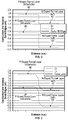
- FIG. 2 is an illustration of an exemplary band offset diagram for the disclosed tunnel junction 26 ( FIG. 1 ), and FIG. 3 is the band offset diagram shown in FIG. 2 after thermal equilibrium.
- the band offset diagrams shown in FIGS. 2-3 illustrate a valence band E v and a conduction band E c of both the p-doped tunnel layer 60 as well as the n-doped tunnel layer 62 of the tunnel junction 26, as well as a valence band (VB) edge.
- both the valence band E v and the conduction band E c both bend between the p-doped tunnel layer 60 and the n-doped tunnel layer 62.
- Joining the p-doped tunnel layer 60 and the n-doped tunnel layer 62 creates a staggered gap (type II) heterostructure.
- both the valence band E v and the conduction band E c of the n-doped tunnel layer 62 are lower in energy when compared to the p-doped tunnel layer 60.
- a heterojunction includes two or more semiconductor materials that are grown on one another, and a heterostructure includes the heterojunction. It should be appreciated that a type II heterostructure results in a lower effective energy barrier for tunneling.
- FIG. 4 is a graph illustrating measured characteristics for an exemplary tunnel junction 26 after annealing. Specifically, the tunnel junction 26 was exposed to a thirty minute anneal at temperatures comparable to those experienced for active junction growth. It should be appreciated that there was negligible or no change in performance of the tunnel junction 26 before or after annealing, which is an indication that the dopants used for both the p-doped tunnel layer 60 and the n-doped tunnel layer 62 ( FIG. 1 ) do not readily diffuse. As seen in FIG. 3 , the tunnel junction 26 may include a peak tunneling current of 372 A/cm 2 and a specific resistance of 0.55 m ⁇ -cm 2 . The peak tunneling current is equivalent to a solar cell operating at more than 30,000 suns, which is well in excess of a practical concentration.
- FIG. 5 is an alternative embodiment of a semiconductor device 100.
- the semiconductor device 100 includes a similar structure as the device shown in FIG. 1 , except that a n-doped tunnel layer 162 is now constructed of AlGaInAs instead of InP.
- a n-doped tunnel layer 162 is now constructed of AlGaInAs instead of InP.
- the n-doped tunnel layer 162 may be doped with relatively high levels of silicon, tellurium, or a combination of both materials. That is, the n-doped tunnel layer 62 may include a doping concentration of at least about 10 19 /cm 3 of silicon, tellurium, or a combination of both materials.
- the n-doped tunnel layer 162 may include a lower bandgap and a higher light absorbance than the n-doped tunnel layer 62 ( FIG. 1 ); however the lower bandgap of the n-doped tunnel layer 162 reduces the energy barrier to tunneling, which in turn exponentially increases the probability of tunneling and tunneling current density.
- the n-doped tunnel layer 162 may include a bandgap of about 0.73 eV.
- light absorption of the n-doped tunnel layer 162 may be mitigated by reducing the thickness of the n-doped tunnel layer, and by decreasing the Al content.
- the thickness of the tunnel junction 26 may be reduced to a minimum of about 10 nm, and the amount of aluminium in the n-doped tunnel layer 162 may range from about zero (i.e., negligible amounts) to about 50%.
- FIG. 6 is an illustration of an exemplary band offset diagram for the disclosed tunnel junction 26 shown in FIG. 5
- FIG. 7 is the band offset diagram shown in FIG. 7 after thermal equilibrium.
- aluminium may be added to the n-doped tunnel layer 162 to create an n+ AlGaInAs layer as well.
- the disclosed tunnel junction includes the p-doped tunnel layer constructed of AlGaAsSb, which demonstrates improved performance characteristics when compared to some other tunnel junctions currently available.
- the disclosed p-doped layer may be easier to grow, since AlGaAsSb may be doped more heavily with carbon.
- compounds containing a high amount of indium are typically challenging to dope.
- a p-doped InAlGaAs layer may only be capable of being doped to the level of about 10 18 /cm 3 , and even this level of doping may be challenging.
- the disclosed tunnel junction also exhibits relatively high peak tunneling currents.
- the disclosed p-doped tunnel layer constructed of AlGaAsSb also exhibits a higher bandgap (i.e., transparency) than some other types of tunnel junctions currently available.
- high transparency is especially important in applications where the tunnel junction is placed in the upper portion of a solar cell that is located closer to incident light (i.e., the sun).
Landscapes
- Photovoltaic Devices (AREA)
- Engineering & Computer Science (AREA)
- Life Sciences & Earth Sciences (AREA)
- Sustainable Energy (AREA)
- Manufacturing & Machinery (AREA)
- Insulated Gate Type Field-Effect Transistor (AREA)
- Bipolar Transistors (AREA)
- Sustainable Development (AREA)
Abstract
Description
- The disclosed system and method relate to a semiconductor device and, more particularly, to a semiconductor device including a tunnel junction that has a n-doped tunnel layer and a p-doped tunnel layer, where the p-doped tunnel layer is constructed of aluminum gallium arsenide antimonide (AlGaAsSb).
- Wafer bonding technology may be used to monolithically join two materials with different lattice structures together. Wafer bonding technology has great potential. For example, joining gallium arsenide (GaAs) or indium phosphide (InP) based materials to other semiconductor materials may result in the integration of optical, photovoltaic, and electronic devices and enhance the performance of computers, solar cells, light emitting diodes and other electronic devices. In one specific example, a five-junction (5J) cell, which is created by bonding a three-junction (3J) GaAs-based cell with a two-junction (2J) InP-based cell, results in a terrestrial solar cell having an efficiency of about 39% and a space solar cell having an efficiency of about 36%.
- One requirement for an InP-based multi-junction solar cell is a high transparency (which is also referred to as bandgap) tunnel junction. The tunnel junctions currently available that are employed in InP-based multi-junction solar cells may sometimes absorb high amounts of light, or have very low peak tunneling currents. For example, one type of tunnel junction that is currently available includes a n-doped InP layer and a p-doped InAlGaAs layer. However, this tunnel junction may not always be easy to grow. This is because compounds containing a large amount of indium, such as InAlGaAs, are typically challenging to dope p-type. Furthermore, this type of tunnel junction may have a limited peak tunnel current as well. In another approach, a tunnel junction having a p-doped gallium arsenide antimonide (GaAsSb) layer and a n-doped indium gallium arsenide (InGaAs) layer may be used. This tunnel juction has a relatively high peak tunnel current, but both layers of this tunnel junction may also absorb light that is intended for active junctions of the solar cell. Thus, there exists a need in the art for a semiconductor device having a tunnel junction that is relatively easy to dope, has a relatively high transparency, and a relatively high peak tunnel current.
- In one embodiment, a tunnel junction for a semiconductor device is disclosed. The tunnel junction includes a n-doped tunnel layer and a p-doped tunnel layer. The p-doped tunnel layer is constructed of aluminum gallium arsenide antimonide (AlGaAsSb).
- In another embodiment, a semiconductor device is disclosed. The semiconductor device includes a first subcell, a second subcell, and a tunnel junction for electrically connecting the first subcell and the second subcell together in electrical series. The tunnel junction includes a n-doped tunnel layer and a p-doped tunnel layer. The p-doped tunnel layer is constructed of aluminum gallium arsenide antimonide (AlGaAsSb) and is doped with carbon.
- In yet another embodiment, a method of constructing a photovoltaic device is disclosed. The method includes growth of a n-doped tunnel layer and a p-doped tunnel layer. The p-doped tunnel layer is constructed of aluminum gallium arsenide antimonide (AlGaAsSb).
- Other objects and advantages of the disclosed method and system will be apparent from the following description, the accompanying drawings and the appended claims.
-
-
FIG. 1 is an illustration of an exemplary semiconductor device including the disclosed tunnel junction; -
FIG. 2 is an illustration of an exemplary band offset diagram for the disclosed tunnel junction shown inFIG. 1 ; -
FIG. 3 is the band offset diagram shown inFIG. 2 after thermal equilibrium; -
FIG. 4 is a graph illustrating measured current and voltage for an exemplary tunnel junction after annealing; -
FIG. 5 is an illustration of an alternative embodiment of the semiconductor device shown inFIG. 1 having a different n-doped tunnel layer; -
FIG. 6 is an illustration of an exemplary band offset diagram for the disclosed tunnel junction shown inFIG. 5 ; and -
FIG. 7 is the band offset diagram shown inFIG. 6 after thermal equilibrium. -
FIG. 1 is an illustration of an embodiment of the disclosedsemiconductor device 10. In the embodiment as shown, thesemiconductor device 10 is a solar cell, and in particular an indium phosphide (InP)-based dual-junction solar cell, meaning thesemiconductor device 10 includes two photovoltaic cells (which are also referred to as subcells). Specifically, thesemiconductor device 10 may include a firstphotovoltaic cell 22, a secondphotovoltaic cell 24, and the disclosedtunnel junction 26, which is located between the firstphotovoltaic cell 22 and the secondphotovoltaic cell 24. As explained in greater detail below, thetunnel junction 26 may include a n-doped tunnel layer and a p-doped tunnel layer, where the p-doped tunnel layer is constructed of aluminum gallium arsenide antimonide (AlGaAsSb). Furthermore, it should be appreciated that thetunnel junction 26 may be referred to as a p-n junction. AlthoughFIG. 1 illustrates a solar cell, it is to be appreciated that the semiconductor device is not limited to just a solar cell. Indeed, thetunnel junction 26 may be used in a variety of optoelectronic devices such as, but not limited to, semiconductor lasers, laser power converters, and sensors. - The first
photovoltaic cell 22 may include a first emitter andbase 20. In one exemplary embodiment, the first emitter andbase 20 is an indium gallium arsenide phosphide (GaInPAs) emitter. In another embodiment, the first emitter and base 220 may be III-V material such as, but not limited to, aluminum arsenide antimonide (AlAsSb), AlGaAsSb, aluminum indium arsenide (AlInAs), indium phosphide (InP), aluminum gallium indium arsenide (AlGaInAs), gallium indium arsenide (GaInAs), or gallium arsenide antimonide (GaAsSb). In one embodiment, the first emitter andbase 20 includes a separate emitter layer and base layer (not shown), where the emitter layer is nearest to incident light. - In the non-limiting embodiment as shown, the first
photovoltaic cell 22 includes a bandgap of 1.1 eV. In another embodiment, the firstphotovoltaic cell 22 may include a bandgap of from about 0.73 to 2.45 eV. In yet another embodiment, the firstphotovoltaic cell 22 may include a bandgap of from about 1.0 to 1.1 eV and may be included in a three or more junction solar cell. The firstphotovoltaic cell 22 may be sensitive to a first-photoactive-subcell-layer wavelength. As used herein, the term wavelength may mean a single discrete wavelength, or, wavelength may include a range of wavelengths at which the layer material achieves a good light-to-electricity conversion efficiency. - The first
photovoltaic cell 22 may also include awindow layer 28. Thewindow layer 28 may be disposed on afirst side 30 of the first emitter andbase 20, which would be positioned nearest to incident light L. As used herein, the relative terms top and bottom are used to indicate the surface nearest to and farthest from the incident light L, respectively. Also, when used to compare two layers, upper or above or overlying may refer to a layer closer to the sun, and lower or below or underlying may refer to a layer further from the sun or other source of illumination. Thewindow layer 28 may be an InP, AlGaInAs, AlInAs, AlAsSb, AlGaAsSb, or a GaInPAs composition that provides bandgap energy greater than about 1.1 eV. Thewindow layer 28 has two functions. The first function of thewindow layer 28 is to reduce minority-carrier recombination (i.e., to passivate) on afront surface 32 of the firstphotovoltaic cell 22. Additionally, the optical properties of the window material must be such that as much light as possible is transmitted to the firstphotovoltaic cell 22, and any additional photoactive subcell layers that may be disposed underneath thereof (not shown), where the photogenerated charge carriers may be collected more efficiently. If there is substantial light absorption in thewindow layer 28, carriers generated in the window layer are less likely to be subsequently collected and hence light absorption in the window degrades overall conversion efficiency. - The
semiconductor device 10 may optionally include an antireflection (AR) layer or coating (not shown) disposed on thefront surface 32 of thesemiconductor device 10 nearest the incident light L, which is shown impinging from the direction indicated by the arrows. In one embodiment, the AR coating may be disposed atop thewindow layer 28. The AR coating may reduce surface reflections between the optically transparent media above the semiconductor device 10 (such as air, glass, or polymer) and various semiconductor layers of thesemiconductor device 10, thereby enabling more photons to enter thesemiconductor device 10. The AR coating may be constructed of materials such as, for example, titanium dioxide (TiO2), tantalum pentoxide (Ta2O5), silicon dioxide (SiO2), and magnesium fluoride (MgF2). The thickness of the AR coating may vary, but may range between about 0.04 and 0.35 microns. While an AR coating can be applied to thesemiconductor device 10, in other embodiments another subcell may be stacked or applied above thesemiconductor device 10. - The first
photovoltaic cell 22 may further include a p-doped back surface field (BSF)layer 34 disposed on abottom surface 36 of the first emitter andbase 20. In the exemplary embodiment as illustrated, the p-dopedBSF layer 34 is a p-doped InP BSF layer. In another embodiment, the p-dopedBSF layer 34 may be an AlGaInAs, GaAsSb, AlAsSb, AlGaAsSb, AlInAs, GaInPAs and their alloys layer. In one embodiment, theBSF layer 34 is lattice-matched to InP. In another embodiment, theBSF layer 34 may be a coherently strained layer with a thickness below a Matthews-Blakeslee critical thickness. - The second
photovoltaic cell 24 includes a second emitter andbase 40. In the exemplary embodiment as shown, the second emitter andbase 40 is a GaInPAs layer having an InP lattice constant. In another embodiment, the second emitter andbase 40 may be GaInAs, GaAsSb, AlGaInAs, AlGaAsSb, GaInPAs and their alloys having an InP lattice constant. The second emitter andbase 40 may have a bandgap lower than the bandgap of the first emitter andbase 20. In the exemplary embodiment as shown inFIG. 1 , the secondphotovoltaic cell 24 has a bandgap of about 0.8 eV. In another embodiment, the secondphotovoltaic cell 24 may have a bandgap of from about 0.73 to 2.0 eV. In yet another embodiment, the secondphotovoltaic cell 24 may have a bandgap of from about 0.73 to 0.8 eV and be included in a three or more junction solar cell lattice-matched to InP. - The second photovoltaic cell may 24 further include a n-doped
window layer 42 disposed on atop surface 44 of the second emitter andbase 40. In general, the characteristics of the n-dopedwindow layer 42 are similar to the window characteristics of thewindow layer 28. The n-dopedwindow 42 may include a n-doping concentration of between about 2×10¹⁸/cm3 and 2×10¹⁹/cm3. In another embodiment, the n-dopedwindow 42 has a n-doping concentration of about 1×10¹⁹/cm3 to create a relatively large electric field and to passivate the p-n junction. - The second
photovoltaic cell 24 may further include asecond BSF layer 48 below the second emitter andbase 40, which is similar to theBSF layer 34. Thetunnel junction 26 may electrically connect the firstphotovoltaic cell 22 and the secondphotovoltaic cell 24 together with one another in electrical series. It should also be appreciated that thetunnel junction 26 is a type-II tunnel junction, which reduces the tunneling energy barrier within thetunnel junction 26. This in turn increases tunneling probability as well as the peak tunneling current of thetunnel junction 26. For example, as seen inFIG. 4 , in one embodiment thetunnel junction 26 may include a peak tunneling current of 372 A/cm2 and a specific resistance of 0.55 mΩ-cm2. Furthermore, as explained in greater detail below, both layers of thetunnel junction 26 may be doped at relatively high levels. - In the embodiment as shown in
FIG. 1 , thetunnel junction 26 includes a p-dopedtunnel layer 60 and a n-dopedtunnel layer 62. The p-dopedtunnel layer 60 is constructed of aluminum gallium arsenide antimonide (AlGaAsSb). The p-dopedtunnel layer 60 may be doped with relatively high levels of carbon (i.e., C-doping or carbon doping). That is, the p-dopedtunnel layer 60 may include a C-doping concentration ranging from about 1019/cm3 to 2×10²⁰/cm3. It is to be appreciated that carbon doping employs dopants that include relatively low diffusion coefficients, thereby resulting in relatively stable doping profiles and tunnel juction performance. However, an indium-based material such as, for example, an InAlGaAs layer may be challenging to dope because indium precursors may inhibit the incorporation of carbon dopants. - It should also be appreciated that the p-doped
tunnel layer 60 may be lattice-matched with the p-dopedInP BSF layer 34. The inclusion of antimonide in the p-dopedtunnel layer 60 allows for lattice-matching with the p-dopedInP BSF layer 34. Furthermore, the inclusion of aluminium within the p-dopedtunnel layer 60 results in a relatively high bandgap (i.e., transparency) and a low level of light absorption. A relatively high bandgap may be any value greater than about 0.73 eV. In one embodiment, the p-dopedtunnel layer 60 may include bandgap ranging from about 0.7 to about 1.4 eV. - The n-doped
tunnel layer 62 may also be lattice-matched to InP. In one embodiment, the n-dopedtunnel layer 62 is high bandgap III-V semiconductor having an InP lattice constant and that may form type II band alignment with the p-dopedtunnel layer 60. In another embodiment, the n-dopedtunnel layer 62 may be a highly n-doped InP, aluminium indium phosphide arsenic (AlInPAs), AlAsSb, or AlGaAsSb tunnel layer having a bandgap greater than or equal to 1.35 eV and an InP lattice constant. In one embodiment, the n-dopedtunnel layer 62 is an InP tunnel layer having a bandgap of 1.35 eV. The n-dopedtunnel layer 62 may be doped with relatively high levels of silicon or tellurium (i.e., Si or Te-doping). That is, the n-dopedtunnel layer 62 may include an Si or Te-doping concentration of at least about 1019/cm3. - In one embodiment, the p-doped
tunnel layer 60 and the n-dopedtunnel layer 62 may be grown sequentially in a metalorganic vapor phase epitaxy (MOVPE) reactor. Furthermore, thesemiconductor device 10 as well as various device components (e.g., the window, BSF) are grown in a MOVPE reactor. In another embodiment, thetunnel junction 26 may be grown in a chemical beam epitaxy (CBE), hydride vapor phase epitaxy (HVPE) or atomic layer deposition (ALD) reactor. In the embodiment as shown inFIG. 1 , thesemiconductor device 10 is an upright solar cell configuration where new layers are grown just above a prior layer, and the highest bandgap layer is grown last. In another embodiment, thesemiconductor device 10 may be inverted, where the highest bandgap layer is grown first. -
FIG. 2 is an illustration of an exemplary band offset diagram for the disclosed tunnel junction 26 (FIG. 1 ), andFIG. 3 is the band offset diagram shown inFIG. 2 after thermal equilibrium. The band offset diagrams shown inFIGS. 2-3 illustrate a valence band Ev and a conduction band Ec of both the p-dopedtunnel layer 60 as well as the n-dopedtunnel layer 62 of thetunnel junction 26, as well as a valence band (VB) edge. In the exemplary embodiment as described, the p-dopedtunnel layer 60 includes a 20% concentration of aluminium (i.e., x = 0.20). Turning toFIG. 3 at thermal equilibrium, after carrier diffusion, it can be seen that both the valence band Ev and the conduction band Ec both bend between the p-dopedtunnel layer 60 and the n-dopedtunnel layer 62. Joining the p-dopedtunnel layer 60 and the n-dopedtunnel layer 62 creates a staggered gap (type II) heterostructure. Indeed, as seen inFIGS. 3 and4 , both the valence band Ev and the conduction band Ec of the n-dopedtunnel layer 62 are lower in energy when compared to the p-dopedtunnel layer 60. A heterojunction includes two or more semiconductor materials that are grown on one another, and a heterostructure includes the heterojunction. It should be appreciated that a type II heterostructure results in a lower effective energy barrier for tunneling. -
FIG. 4 is a graph illustrating measured characteristics for anexemplary tunnel junction 26 after annealing. Specifically, thetunnel junction 26 was exposed to a thirty minute anneal at temperatures comparable to those experienced for active junction growth. It should be appreciated that there was negligible or no change in performance of thetunnel junction 26 before or after annealing, which is an indication that the dopants used for both the p-dopedtunnel layer 60 and the n-doped tunnel layer 62 (FIG. 1 ) do not readily diffuse. As seen inFIG. 3 , thetunnel junction 26 may include a peak tunneling current of 372 A/cm2 and a specific resistance of 0.55 mΩ-cm2. The peak tunneling current is equivalent to a solar cell operating at more than 30,000 suns, which is well in excess of a practical concentration. -
FIG. 5 is an alternative embodiment of asemiconductor device 100. Thesemiconductor device 100 includes a similar structure as the device shown inFIG. 1 , except that a n-dopedtunnel layer 162 is now constructed of AlGaInAs instead of InP. Thus, it is to be appreciated that thesemiconductor device 100 retains the relatively high bandgap and the low level of light absorption of the p-dopedtunnel layer 60 as described above and illustrated inFIG. 1 . The n-dopedtunnel layer 162 may be doped with relatively high levels of silicon, tellurium, or a combination of both materials. That is, the n-dopedtunnel layer 62 may include a doping concentration of at least about 1019/cm3 of silicon, tellurium, or a combination of both materials. - It is to be appreciated that the n-doped
tunnel layer 162 may include a lower bandgap and a higher light absorbance than the n-doped tunnel layer 62 (FIG. 1 ); however the lower bandgap of the n-dopedtunnel layer 162 reduces the energy barrier to tunneling, which in turn exponentially increases the probability of tunneling and tunneling current density. Specifically, in one embodiment, the n-dopedtunnel layer 162 may include a bandgap of about 0.73 eV. Furthermore, light absorption of the n-dopedtunnel layer 162 may be mitigated by reducing the thickness of the n-doped tunnel layer, and by decreasing the Al content. Specifically, in one embodiment the thickness of thetunnel junction 26 may be reduced to a minimum of about 10 nm, and the amount of aluminium in the n-dopedtunnel layer 162 may range from about zero (i.e., negligible amounts) to about 50%. -
FIG. 6 is an illustration of an exemplary band offset diagram for the disclosedtunnel junction 26 shown inFIG. 5 , andFIG. 7 is the band offset diagram shown inFIG. 7 after thermal equilibrium. In the exemplary embodiment as described, the p-dopedtunnel layer 60 includes a 20% concentration of aluminium (i.e., x = 0.20), and the n-dopedtunnel layer 162 is constructed of GaInAs. However, it is to be understood that aluminium may be added to the n-dopedtunnel layer 162 to create an n+ AlGaInAs layer as well. - Referring generally to the figures, the disclosed tunnel junction includes the p-doped tunnel layer constructed of AlGaAsSb, which demonstrates improved performance characteristics when compared to some other tunnel junctions currently available. Specifically, the disclosed p-doped layer may be easier to grow, since AlGaAsSb may be doped more heavily with carbon. In contrast, compounds containing a high amount of indium are typically challenging to dope. In fact, a p-doped InAlGaAs layer may only be capable of being doped to the level of about 1018/cm3, and even this level of doping may be challenging. Furthermore, the disclosed tunnel junction also exhibits relatively high peak tunneling currents. Finally, it should also be appreciated that the disclosed p-doped tunnel layer constructed of AlGaAsSb also exhibits a higher bandgap (i.e., transparency) than some other types of tunnel junctions currently available. Finally, it is to be appreciated that high transparency is especially important in applications where the tunnel junction is placed in the upper portion of a solar cell that is located closer to incident light (i.e., the sun).
- Further, the disclosure comprises embodiments according to the following clauses:
- Clause 1: A tunnel junction for a semiconductor device, comprising: a n-doped tunnel layer; and a p-doped tunnel layer, wherein the p-doped tunnel layer is constructed of aluminum gallium arsenide antimonide (AlGaAsSb).
- Clause 2: The tunnel junction of
clause 1, wherein the p-doped tunnel layer is doped with carbon. - Clause 3: The tunnel junction of clause 2, wherein the p-doped tunnel layer includes a carbon concentration ranging from about 1019/cm3 to 2×10²⁰/cm3.
- Clause 4: The tunnel junction of
clause 1, wherein the p-doped tunnel layer includes bandgap ranging from about 0.7 to about 1.4 eV. - Clause 5: The tunnel junction of
clause 1, wherein the n-doped tunnel layer is a n-doped material selected from the group consisting of: indium phosphide (InP), aluminium indium phosphide arsenic (AlInPAs), aluminum arsenide antimonide (AlAsSb), and AlGaAsSb. - Clause 6: The tunnel junction of
clause 1, wherein the n-doped tunnel layer is doped with a material selected from a group consisting of: silicon and tellurium. - Clause 7: The tunnel junction of clause 6, wherein the n-doped tunnel layer includes a silicon concentration or a tellurium concentration of at least about 1019/cm3.
- Clause 8: The tunnel junction of
clause 1, wherein the n-doped tunnel layer is constructed of aluminum gallium indium arsenide (AlGaInAs). - Clause 9: The tunnel junction of clause 8, wherein the n-doped tunnel layer is doped with at least one of silicon and tellurium.
- Clause 10: A semiconductor device, comprising: a first subcell; a second subcell; and a tunnel junction for electrically connecting the first subcell and the second subcell together in electrical series, wherein the tunnel junction includes a n-doped tunnel layer and a p-doped tunnel layer, and wherein the p-doped tunnel layer is constructed of aluminum gallium arsenide antimonide (AlGaAsSb) and is doped with carbon.
- Clause 11: The semiconductor device of
clause 10, wherein the p-doped tunnel layer includes a carbon concentration ranging from about 1019/cm3 to 2×10²⁰/cm3. - Clause 12: The semiconductor device of
clause 10, wherein the p-doped tunnel layer includes a bandgap ranging from about 0.7 to about 1.4 eV. - Clause 13: The semiconductor device of
clause 10, wherein the n-doped tunnel layer is a n-doped material selected from the group consisting of: indium phosphide (InP), aluminium indium phosphide arsenic (AlInPAs), aluminum arsenide antimonide (AlAsSb), and AlGaAsSb. - Clause 14: The semiconductor device of
clause 10, wherein the n-doped tunnel layer is doped with a material selected from a group consisting of: silicon and tellurium. - Clause 15: The semiconductor device of clause 14, wherein the n-doped tunnel layer includes a silicon concentration or a tellurium concentration of at least about 1019/cm3.
- Clause 16: The semiconductor device of
clause 10, wherein the n-doped tunnel layer is constructed of aluminum gallium indium arsenide (AlGaInAs). - Clause 17: The semiconductor device of clause 16, wherein the n-doped tunnel layer is doped with at least one of silicon and tellurium.
- Clause 18: A method of constructing a photovoltaic device, comprising: growing a n-doped tunnel layer; and growing a p-doped tunnel layer, wherein the p-doped tunnel layer is constructed of aluminum gallium arsenide antimonide (AlGaAsSb).
- Clause 19: The method as recited in clause 18, comprising doping the p-doped tunnel layer with carbon.
- Clause 20: The method as recited in clause 18, wherein the n-doped tunnel layer and the p-doped tunnel layer are grown sequentially in a reactor selected from the group consisting of a: metalorganic vapor phase epitaxy (MOVPE) reactor, a chemical beam epitaxy (CBE) reactor, a hydride vapor phase epitaxy (HVPE) reactor and an atomic layer deposition (ALD) reactor.
- While the forms of apparatus and methods herein described constitute preferred embodiments of this invention, it is to be understood that the invention is not limited to these precise forms of apparatus and methods, and that changes may be made therein without departing from the scope of the invention.
Claims (12)
- A tunnel junction (26) for a semiconductor device (10, 100), comprising:a n-doped tunnel layer (62, 162); anda p-doped tunnel layer (60), wherein the p-doped tunnel layer is constructed of aluminum gallium arsenide antimonide (AlGaAsSb).
- The tunnel junction of claim 1, wherein the p-doped tunnel layer is doped with carbon.
- The tunnel junction of claim 2, wherein the p-doped tunnel layer includes a carbon concentration ranging from about 1019/cm3 to 2×10²⁰/cm3.
- The tunnel junction of any one of claims 1-2, wherein the p-doped tunnel layer includes bandgap ranging from about 0.7 to about 1.4 eV.
- The tunnel junction of any one of claims 1, 2 or 4, wherein the n-doped tunnel layer is a n-doped material selected from the group consisting of: indium phosphide (InP), aluminium indium phosphide arsenic (AlInPAs), aluminum arsenide antimonide (AlAsSb), and AlGaAsSb.
- The tunnel junction of any one of claims 1, 2, 4, or 5, wherein the n-doped tunnel layer is doped with a material selected from a group consisting of: silicon and tellurium.
- The tunnel junction of claim 6, wherein the n-doped tunnel layer includes a silicon concentration or a tellurium concentration of at least about 1019/cm3.
- The tunnel junction of any one of claims 1, 2, or 4-6 wherein the n-doped tunnel layer is constructed of aluminum gallium indium arsenide (AlGaInAs).
- The tunnel junction of claim 8, wherein the n-doped tunnel layer is doped with at least one of silicon and tellurium.
- A method of constructing a photovoltaic device (10, 100), comprising:growing a n-doped tunnel layer 62, 162); andgrowing a p-doped tunnel layer (60), wherein the p-doped tunnel layer is constructed of aluminum gallium arsenide antimonide (AlGaAsSb).
- The method as recited in claim 10, comprising doping the p-doped tunnel layer with carbon.
- The method as recited in any one of claims 10-11, wherein the n-doped tunnel layer and the p-doped tunnel layer are grown sequentially in a reactor selected from the group consisting of a: metalorganic vapor phase epitaxy (MOVPE) reactor, a chemical beam epitaxy (CBE) reactor, a hydride vapor phase epitaxy (HVPE) reactor and an atomic layer deposition (ALD) reactor.
Applications Claiming Priority (1)
| Application Number | Priority Date | Filing Date | Title |
|---|---|---|---|
| US14/860,214 US20170084771A1 (en) | 2015-09-21 | 2015-09-21 | Antimonide-based high bandgap tunnel junction for semiconductor devices |
Publications (2)
| Publication Number | Publication Date |
|---|---|
| EP3144979A1 true EP3144979A1 (en) | 2017-03-22 |
| EP3144979B1 EP3144979B1 (en) | 2024-05-08 |
Family
ID=56693939
Family Applications (1)
| Application Number | Title | Priority Date | Filing Date |
|---|---|---|---|
| EP16178410.3A Active EP3144979B1 (en) | 2015-09-21 | 2016-07-07 | Antimonide-based high bandgap tunnel junction for semiconductor devices |
Country Status (6)
| Country | Link |
|---|---|
| US (1) | US20170084771A1 (en) |
| EP (1) | EP3144979B1 (en) |
| JP (1) | JP6920037B2 (en) |
| KR (1) | KR102644800B1 (en) |
| CN (1) | CN106549069B (en) |
| TW (1) | TWI775725B (en) |
Families Citing this family (6)
| Publication number | Priority date | Publication date | Assignee | Title |
|---|---|---|---|---|
| DE102017005950A1 (en) | 2017-06-21 | 2018-12-27 | Azur Space Solar Power Gmbh | solar cell stack |
| FR3083405B1 (en) * | 2018-06-28 | 2020-07-31 | Airbus Defence & Space Sas | SOLAR SATELLITE GENERATOR TEST DEVICE |
| CN110233187B (en) * | 2019-06-19 | 2022-01-25 | 扬州乾照光电有限公司 | Lattice mismatched multi-junction solar cell structure |
| CN114744484B (en) * | 2022-04-08 | 2024-03-26 | 青岛科技大学 | high-power laser structure based on GaAs-based high-band-gap tunnel junction |
| CN115172500B (en) * | 2022-07-12 | 2023-08-15 | 中国电子科技集团公司第十八研究所 | A laser battery component |
| CN115313155B (en) * | 2022-08-30 | 2025-02-07 | 电子科技大学 | A multi-junction vertical cavity surface emitting laser with heterogeneous tunnel junction and a preparation method thereof |
Citations (1)
| Publication number | Priority date | Publication date | Assignee | Title |
|---|---|---|---|---|
| US20050253164A1 (en) * | 2004-05-17 | 2005-11-17 | Rajaram Bhat | Tunnel junctions for long-wavelength vcsels |
Family Cites Families (21)
| Publication number | Priority date | Publication date | Assignee | Title |
|---|---|---|---|---|
| US4195305A (en) * | 1978-09-25 | 1980-03-25 | Varian Associates, Inc. | Lattice constant grading in the Aly Ga1-y As1-x Sbx alloy system |
| US5019177A (en) * | 1989-11-03 | 1991-05-28 | The United States Of America As Represented By The United States Department Of Energy | Monolithic tandem solar cell |
| US5679963A (en) * | 1995-12-05 | 1997-10-21 | Sandia Corporation | Semiconductor tunnel junction with enhancement layer |
| US5944913A (en) * | 1997-11-26 | 1999-08-31 | Sandia Corporation | High-efficiency solar cell and method for fabrication |
| JP2001044456A (en) * | 1999-07-27 | 2001-02-16 | Japan Energy Corp | Solar cell manufacturing method |
| GB2358959B (en) * | 1999-10-07 | 2002-01-16 | Win Semiconductors Corp | Metamorphic heterojunction bipolar transistor having material structure for low cost fabrication on large size gallium arsenide wafers |
| US6765238B2 (en) * | 2002-09-12 | 2004-07-20 | Agilent Technologies, Inc. | Material systems for semiconductor tunnel-junction structures |
| US20050253222A1 (en) * | 2004-05-17 | 2005-11-17 | Caneau Catherine G | Semiconductor devices on misoriented substrates |
| US20060048811A1 (en) * | 2004-09-09 | 2006-03-09 | Krut Dimitri D | Multijunction laser power converter |
| US20090078310A1 (en) * | 2007-09-24 | 2009-03-26 | Emcore Corporation | Heterojunction Subcells In Inverted Metamorphic Multijunction Solar Cells |
| WO2009067347A1 (en) * | 2007-11-20 | 2009-05-28 | Arizona Board Of Regents, Acting For And On Behalf Of Arizona State University | Lattice matched multi- junction photovoltaic and optoelectronic devices |
| JP5167860B2 (en) * | 2008-02-26 | 2013-03-21 | 住友電気工業株式会社 | Surface emitting semiconductor laser and method for fabricating surface emitting laser |
| CN101431117A (en) * | 2008-11-24 | 2009-05-13 | 北京索拉安吉清洁能源科技有限公司 | Multi-junction solar cell with doping blocking layer |
| US11417788B2 (en) * | 2010-11-19 | 2022-08-16 | The Boeing Company | Type-II high bandgap tunnel junctions of InP lattice constant for multijunction solar cells |
| US10170652B2 (en) * | 2011-03-22 | 2019-01-01 | The Boeing Company | Metamorphic solar cell having improved current generation |
| JP5634955B2 (en) * | 2011-07-08 | 2014-12-03 | シャープ株式会社 | III-V compound semiconductor film manufacturing method and compound semiconductor solar cell manufacturing method |
| CN102983208B (en) * | 2011-09-07 | 2017-07-28 | 索埃尔科技公司 | Grid design for III V compound semiconductor cells |
| WO2013074530A2 (en) * | 2011-11-15 | 2013-05-23 | Solar Junction Corporation | High efficiency multijunction solar cells |
| KR20140121463A (en) * | 2012-01-31 | 2014-10-15 | 다우 글로벌 테크놀로지스 엘엘씨 | Method of making photovoltaic devices with reduced conduction band offset between pnictide absorber films and emitter films |
| CN102832285A (en) * | 2012-09-07 | 2012-12-19 | 天津三安光电有限公司 | Three-junction solar battery and preparation method thereof |
| JP6550691B2 (en) * | 2013-07-30 | 2019-07-31 | 株式会社リコー | Compound semiconductor solar cell |
-
2015
- 2015-09-21 US US14/860,214 patent/US20170084771A1/en not_active Abandoned
-
2016
- 2016-07-07 EP EP16178410.3A patent/EP3144979B1/en active Active
- 2016-07-20 KR KR1020160091755A patent/KR102644800B1/en active Active
- 2016-07-20 TW TW105122866A patent/TWI775725B/en active
- 2016-08-18 CN CN201610692063.7A patent/CN106549069B/en active Active
- 2016-09-12 JP JP2016177314A patent/JP6920037B2/en active Active
Patent Citations (1)
| Publication number | Priority date | Publication date | Assignee | Title |
|---|---|---|---|---|
| US20050253164A1 (en) * | 2004-05-17 | 2005-11-17 | Rajaram Bhat | Tunnel junctions for long-wavelength vcsels |
Non-Patent Citations (2)
| Title |
|---|
| AGERT C ET AL: "NOVEL DEVICE STRUCTURES FOR INFRARED SOLAR CELLS BASED ON GaSb: PN-HOMOJUNCTIONS, PN-HETEROJUNCTIONS, AND TANDEM CELLS", PROCEEDINGS OF THE 17TH EUROPEAN PHOTOVOLTAIC SOLAR ENERGY CONFERENCE, vol. CONF. 17, 22 October 2001 (2001-10-22) - 26 October 2001 (2001-10-26), MUNICH, GERMANY, pages 372 - 375, XP001139446, ISBN: 978-3-936338-08-9 * |
| TIMMONS M L ET AL: "GaAsSb and AlGaAsSB tunnel diodes", JOURNAL OF APPLIED PHYSICS, vol. 52, no. 2, February 1981 (1981-02-01), pages 1134 - 1135, XP000819834, ISSN: 0021-8979, DOI: 10.1063/1.328816 * |
Also Published As
| Publication number | Publication date |
|---|---|
| KR20170034763A (en) | 2017-03-29 |
| KR102644800B1 (en) | 2024-03-06 |
| CN106549069B (en) | 2021-08-17 |
| US20170084771A1 (en) | 2017-03-23 |
| CN106549069A (en) | 2017-03-29 |
| JP2017108106A (en) | 2017-06-15 |
| EP3144979B1 (en) | 2024-05-08 |
| JP6920037B2 (en) | 2021-08-18 |
| TWI775725B (en) | 2022-09-01 |
| TW201721894A (en) | 2017-06-16 |
Similar Documents
| Publication | Publication Date | Title |
|---|---|---|
| EP2641275B1 (en) | TYPE-II HIGH BANDGAP TUNNEL JUNCTIONS OF InP LATTICE CONSTANT FOR MULTIJUNCTION SOLAR CELLS | |
| US6150603A (en) | Bilayer passivation structure for photovoltaic cells | |
| US8642883B2 (en) | Heterojunction solar cell | |
| US10355159B2 (en) | Multi-junction solar cell with dilute nitride sub-cell having graded doping | |
| EP3144979B1 (en) | Antimonide-based high bandgap tunnel junction for semiconductor devices | |
| US20170110607A1 (en) | Lattice matchable alloy for solar cells | |
| US11527667B2 (en) | Tunnel junctions for multijunction solar cells | |
| WO2017205100A1 (en) | Exponential doping in lattice-matched dilute nitride photovoltaic cells | |
| US20130228216A1 (en) | Solar cell with gradation in doping in the window layer | |
| US20120138130A1 (en) | Tunnel diodes comprising stress-compensated compound semiconductor layers | |
| Dawidowski et al. | Tunnel junction limited performance of InGaAsN/GaAs tandem solar cell | |
| US20190288147A1 (en) | Dilute nitride optical absorption layers having graded doping | |
| Li et al. | > 35% 5-junction space solar cells based on the direct bonding technique | |
| Leong et al. | Growth of 1‐eV GaNAsSb‐based photovoltaic cell on silicon substrate at different As/Ga beam equivalent pressure ratios | |
| EP3980586A1 (en) | Dilute nitride optical absorption layers having graded doping | |
| Volz et al. | Material development for improved 1 eV (GaIn)(NAs) solar cell structures | |
| Francea et al. | High efficiency 6-junction solar cells for the global and direct spectra | |
| Zheng et al. | p-GaSb/n-GaAs heterojunction diodes for TPV and solar cell applications | |
| Jackrel et al. | GaInNAsSb solar cells grown by molecular beam epitaxy | |
| Lumb et al. | Broken-gap quantum-well tunnel junctions grown on GaSb substrates |
Legal Events
| Date | Code | Title | Description |
|---|---|---|---|
| PUAI | Public reference made under article 153(3) epc to a published international application that has entered the european phase |
Free format text: ORIGINAL CODE: 0009012 |
|
| STAA | Information on the status of an ep patent application or granted ep patent |
Free format text: STATUS: REQUEST FOR EXAMINATION WAS MADE |
|
| 17P | Request for examination filed |
Effective date: 20160707 |
|
| AK | Designated contracting states |
Kind code of ref document: A1 Designated state(s): AL AT BE BG CH CY CZ DE DK EE ES FI FR GB GR HR HU IE IS IT LI LT LU LV MC MK MT NL NO PL PT RO RS SE SI SK SM TR |
|
| AX | Request for extension of the european patent |
Extension state: BA ME |
|
| RBV | Designated contracting states (corrected) |
Designated state(s): AL AT BE BG CH CY CZ DE DK EE ES FI FR GB GR HR HU IE IS IT LI LT LU LV MC MK MT NL NO PL PT RO RS SE SI SK SM TR |
|
| STAA | Information on the status of an ep patent application or granted ep patent |
Free format text: STATUS: EXAMINATION IS IN PROGRESS |
|
| 17Q | First examination report despatched |
Effective date: 20200409 |
|
| RAP3 | Party data changed (applicant data changed or rights of an application transferred) |
Owner name: THE BOEING COMPANY |
|
| REG | Reference to a national code |
Ref country code: DE Ref legal event code: R079 Free format text: PREVIOUS MAIN CLASS: H01L0031035200 Ipc: H01L0031068700 Ref country code: DE Ref legal event code: R079 Ref document number: 602016087391 Country of ref document: DE Free format text: PREVIOUS MAIN CLASS: H01L0031035200 Ipc: H01L0031068700 |
|
| GRAP | Despatch of communication of intention to grant a patent |
Free format text: ORIGINAL CODE: EPIDOSNIGR1 |
|
| STAA | Information on the status of an ep patent application or granted ep patent |
Free format text: STATUS: GRANT OF PATENT IS INTENDED |
|
| INTG | Intention to grant announced |
Effective date: 20230623 |
|
| RIC1 | Information provided on ipc code assigned before grant |
Ipc: H01L 29/885 20060101ALI20230609BHEP Ipc: H01L 31/18 20060101ALI20230609BHEP Ipc: H01L 31/0304 20060101ALI20230609BHEP Ipc: H01L 31/0693 20120101ALI20230609BHEP Ipc: H01L 31/0687 20120101AFI20230609BHEP |
|
| GRAJ | Information related to disapproval of communication of intention to grant by the applicant or resumption of examination proceedings by the epo deleted |
Free format text: ORIGINAL CODE: EPIDOSDIGR1 |
|
| STAA | Information on the status of an ep patent application or granted ep patent |
Free format text: STATUS: EXAMINATION IS IN PROGRESS |
|
| INTC | Intention to grant announced (deleted) | ||
| GRAP | Despatch of communication of intention to grant a patent |
Free format text: ORIGINAL CODE: EPIDOSNIGR1 |
|
| STAA | Information on the status of an ep patent application or granted ep patent |
Free format text: STATUS: GRANT OF PATENT IS INTENDED |
|
| INTG | Intention to grant announced |
Effective date: 20231213 |
|
| GRAS | Grant fee paid |
Free format text: ORIGINAL CODE: EPIDOSNIGR3 |
|
| GRAA | (expected) grant |
Free format text: ORIGINAL CODE: 0009210 |
|
| STAA | Information on the status of an ep patent application or granted ep patent |
Free format text: STATUS: THE PATENT HAS BEEN GRANTED |
|
| AK | Designated contracting states |
Kind code of ref document: B1 Designated state(s): AL AT BE BG CH CY CZ DE DK EE ES FI FR GB GR HR HU IE IS IT LI LT LU LV MC MK MT NL NO PL PT RO RS SE SI SK SM TR |
|
| P01 | Opt-out of the competence of the unified patent court (upc) registered |
Effective date: 20240402 |
|
| REG | Reference to a national code |
Ref country code: GB Ref legal event code: FG4D |
|
| REG | Reference to a national code |
Ref country code: CH Ref legal event code: EP |
|
| REG | Reference to a national code |
Ref country code: DE Ref legal event code: R096 Ref document number: 602016087391 Country of ref document: DE |
|
| REG | Reference to a national code |
Ref country code: IE Ref legal event code: FG4D |
|
| REG | Reference to a national code |
Ref country code: LT Ref legal event code: MG9D |
|
| REG | Reference to a national code |
Ref country code: NL Ref legal event code: MP Effective date: 20240508 |
|
| PG25 | Lapsed in a contracting state [announced via postgrant information from national office to epo] |
Ref country code: IS Free format text: LAPSE BECAUSE OF FAILURE TO SUBMIT A TRANSLATION OF THE DESCRIPTION OR TO PAY THE FEE WITHIN THE PRESCRIBED TIME-LIMIT Effective date: 20240908 |
|
| PG25 | Lapsed in a contracting state [announced via postgrant information from national office to epo] |
Ref country code: BG Free format text: LAPSE BECAUSE OF FAILURE TO SUBMIT A TRANSLATION OF THE DESCRIPTION OR TO PAY THE FEE WITHIN THE PRESCRIBED TIME-LIMIT Effective date: 20240508 |
|
| PG25 | Lapsed in a contracting state [announced via postgrant information from national office to epo] |
Ref country code: FI Free format text: LAPSE BECAUSE OF FAILURE TO SUBMIT A TRANSLATION OF THE DESCRIPTION OR TO PAY THE FEE WITHIN THE PRESCRIBED TIME-LIMIT Effective date: 20240508 Ref country code: HR Free format text: LAPSE BECAUSE OF FAILURE TO SUBMIT A TRANSLATION OF THE DESCRIPTION OR TO PAY THE FEE WITHIN THE PRESCRIBED TIME-LIMIT Effective date: 20240508 |
|
| PG25 | Lapsed in a contracting state [announced via postgrant information from national office to epo] |
Ref country code: GR Free format text: LAPSE BECAUSE OF FAILURE TO SUBMIT A TRANSLATION OF THE DESCRIPTION OR TO PAY THE FEE WITHIN THE PRESCRIBED TIME-LIMIT Effective date: 20240809 |
|
| PG25 | Lapsed in a contracting state [announced via postgrant information from national office to epo] |
Ref country code: PT Free format text: LAPSE BECAUSE OF FAILURE TO SUBMIT A TRANSLATION OF THE DESCRIPTION OR TO PAY THE FEE WITHIN THE PRESCRIBED TIME-LIMIT Effective date: 20240909 |
|
| REG | Reference to a national code |
Ref country code: AT Ref legal event code: MK05 Ref document number: 1685750 Country of ref document: AT Kind code of ref document: T Effective date: 20240508 |
|
| PG25 | Lapsed in a contracting state [announced via postgrant information from national office to epo] |
Ref country code: NL Free format text: LAPSE BECAUSE OF FAILURE TO SUBMIT A TRANSLATION OF THE DESCRIPTION OR TO PAY THE FEE WITHIN THE PRESCRIBED TIME-LIMIT Effective date: 20240508 |
|
| PG25 | Lapsed in a contracting state [announced via postgrant information from national office to epo] |
Ref country code: ES Free format text: LAPSE BECAUSE OF FAILURE TO SUBMIT A TRANSLATION OF THE DESCRIPTION OR TO PAY THE FEE WITHIN THE PRESCRIBED TIME-LIMIT Effective date: 20240508 |
|
| PG25 | Lapsed in a contracting state [announced via postgrant information from national office to epo] |
Ref country code: AT Free format text: LAPSE BECAUSE OF FAILURE TO SUBMIT A TRANSLATION OF THE DESCRIPTION OR TO PAY THE FEE WITHIN THE PRESCRIBED TIME-LIMIT Effective date: 20240508 |
|
| PG25 | Lapsed in a contracting state [announced via postgrant information from national office to epo] |
Ref country code: PL Free format text: LAPSE BECAUSE OF FAILURE TO SUBMIT A TRANSLATION OF THE DESCRIPTION OR TO PAY THE FEE WITHIN THE PRESCRIBED TIME-LIMIT Effective date: 20240508 |
|
| PG25 | Lapsed in a contracting state [announced via postgrant information from national office to epo] |
Ref country code: LV Free format text: LAPSE BECAUSE OF FAILURE TO SUBMIT A TRANSLATION OF THE DESCRIPTION OR TO PAY THE FEE WITHIN THE PRESCRIBED TIME-LIMIT Effective date: 20240508 |
|
| PG25 | Lapsed in a contracting state [announced via postgrant information from national office to epo] |
Ref country code: PT Free format text: LAPSE BECAUSE OF FAILURE TO SUBMIT A TRANSLATION OF THE DESCRIPTION OR TO PAY THE FEE WITHIN THE PRESCRIBED TIME-LIMIT Effective date: 20240909 Ref country code: PL Free format text: LAPSE BECAUSE OF FAILURE TO SUBMIT A TRANSLATION OF THE DESCRIPTION OR TO PAY THE FEE WITHIN THE PRESCRIBED TIME-LIMIT Effective date: 20240508 Ref country code: NO Free format text: LAPSE BECAUSE OF FAILURE TO SUBMIT A TRANSLATION OF THE DESCRIPTION OR TO PAY THE FEE WITHIN THE PRESCRIBED TIME-LIMIT Effective date: 20240808 Ref country code: NL Free format text: LAPSE BECAUSE OF FAILURE TO SUBMIT A TRANSLATION OF THE DESCRIPTION OR TO PAY THE FEE WITHIN THE PRESCRIBED TIME-LIMIT Effective date: 20240508 Ref country code: LV Free format text: LAPSE BECAUSE OF FAILURE TO SUBMIT A TRANSLATION OF THE DESCRIPTION OR TO PAY THE FEE WITHIN THE PRESCRIBED TIME-LIMIT Effective date: 20240508 Ref country code: IS Free format text: LAPSE BECAUSE OF FAILURE TO SUBMIT A TRANSLATION OF THE DESCRIPTION OR TO PAY THE FEE WITHIN THE PRESCRIBED TIME-LIMIT Effective date: 20240908 Ref country code: HR Free format text: LAPSE BECAUSE OF FAILURE TO SUBMIT A TRANSLATION OF THE DESCRIPTION OR TO PAY THE FEE WITHIN THE PRESCRIBED TIME-LIMIT Effective date: 20240508 Ref country code: GR Free format text: LAPSE BECAUSE OF FAILURE TO SUBMIT A TRANSLATION OF THE DESCRIPTION OR TO PAY THE FEE WITHIN THE PRESCRIBED TIME-LIMIT Effective date: 20240809 Ref country code: FI Free format text: LAPSE BECAUSE OF FAILURE TO SUBMIT A TRANSLATION OF THE DESCRIPTION OR TO PAY THE FEE WITHIN THE PRESCRIBED TIME-LIMIT Effective date: 20240508 Ref country code: ES Free format text: LAPSE BECAUSE OF FAILURE TO SUBMIT A TRANSLATION OF THE DESCRIPTION OR TO PAY THE FEE WITHIN THE PRESCRIBED TIME-LIMIT Effective date: 20240508 Ref country code: BG Free format text: LAPSE BECAUSE OF FAILURE TO SUBMIT A TRANSLATION OF THE DESCRIPTION OR TO PAY THE FEE WITHIN THE PRESCRIBED TIME-LIMIT Effective date: 20240508 Ref country code: AT Free format text: LAPSE BECAUSE OF FAILURE TO SUBMIT A TRANSLATION OF THE DESCRIPTION OR TO PAY THE FEE WITHIN THE PRESCRIBED TIME-LIMIT Effective date: 20240508 Ref country code: RS Free format text: LAPSE BECAUSE OF FAILURE TO SUBMIT A TRANSLATION OF THE DESCRIPTION OR TO PAY THE FEE WITHIN THE PRESCRIBED TIME-LIMIT Effective date: 20240808 |
|
| REG | Reference to a national code |
Ref country code: DE Ref legal event code: R079 Ref document number: 602016087391 Country of ref document: DE Free format text: PREVIOUS MAIN CLASS: H01L0031068700 Ipc: H10F0010142000 |
|
| PG25 | Lapsed in a contracting state [announced via postgrant information from national office to epo] |
Ref country code: DK Free format text: LAPSE BECAUSE OF FAILURE TO SUBMIT A TRANSLATION OF THE DESCRIPTION OR TO PAY THE FEE WITHIN THE PRESCRIBED TIME-LIMIT Effective date: 20240508 |
|
| PG25 | Lapsed in a contracting state [announced via postgrant information from national office to epo] |
Ref country code: EE Free format text: LAPSE BECAUSE OF FAILURE TO SUBMIT A TRANSLATION OF THE DESCRIPTION OR TO PAY THE FEE WITHIN THE PRESCRIBED TIME-LIMIT Effective date: 20240508 |
|
| PG25 | Lapsed in a contracting state [announced via postgrant information from national office to epo] |
Ref country code: CZ Free format text: LAPSE BECAUSE OF FAILURE TO SUBMIT A TRANSLATION OF THE DESCRIPTION OR TO PAY THE FEE WITHIN THE PRESCRIBED TIME-LIMIT Effective date: 20240508 |
|
| PG25 | Lapsed in a contracting state [announced via postgrant information from national office to epo] |
Ref country code: RO Free format text: LAPSE BECAUSE OF FAILURE TO SUBMIT A TRANSLATION OF THE DESCRIPTION OR TO PAY THE FEE WITHIN THE PRESCRIBED TIME-LIMIT Effective date: 20240508 Ref country code: SK Free format text: LAPSE BECAUSE OF FAILURE TO SUBMIT A TRANSLATION OF THE DESCRIPTION OR TO PAY THE FEE WITHIN THE PRESCRIBED TIME-LIMIT Effective date: 20240508 |
|
| PG25 | Lapsed in a contracting state [announced via postgrant information from national office to epo] |
Ref country code: SM Free format text: LAPSE BECAUSE OF FAILURE TO SUBMIT A TRANSLATION OF THE DESCRIPTION OR TO PAY THE FEE WITHIN THE PRESCRIBED TIME-LIMIT Effective date: 20240508 |
|
| PG25 | Lapsed in a contracting state [announced via postgrant information from national office to epo] |
Ref country code: SM Free format text: LAPSE BECAUSE OF FAILURE TO SUBMIT A TRANSLATION OF THE DESCRIPTION OR TO PAY THE FEE WITHIN THE PRESCRIBED TIME-LIMIT Effective date: 20240508 Ref country code: SK Free format text: LAPSE BECAUSE OF FAILURE TO SUBMIT A TRANSLATION OF THE DESCRIPTION OR TO PAY THE FEE WITHIN THE PRESCRIBED TIME-LIMIT Effective date: 20240508 Ref country code: RO Free format text: LAPSE BECAUSE OF FAILURE TO SUBMIT A TRANSLATION OF THE DESCRIPTION OR TO PAY THE FEE WITHIN THE PRESCRIBED TIME-LIMIT Effective date: 20240508 Ref country code: EE Free format text: LAPSE BECAUSE OF FAILURE TO SUBMIT A TRANSLATION OF THE DESCRIPTION OR TO PAY THE FEE WITHIN THE PRESCRIBED TIME-LIMIT Effective date: 20240508 Ref country code: DK Free format text: LAPSE BECAUSE OF FAILURE TO SUBMIT A TRANSLATION OF THE DESCRIPTION OR TO PAY THE FEE WITHIN THE PRESCRIBED TIME-LIMIT Effective date: 20240508 Ref country code: CZ Free format text: LAPSE BECAUSE OF FAILURE TO SUBMIT A TRANSLATION OF THE DESCRIPTION OR TO PAY THE FEE WITHIN THE PRESCRIBED TIME-LIMIT Effective date: 20240508 |
|
| PG25 | Lapsed in a contracting state [announced via postgrant information from national office to epo] |
Ref country code: MC Free format text: LAPSE BECAUSE OF FAILURE TO SUBMIT A TRANSLATION OF THE DESCRIPTION OR TO PAY THE FEE WITHIN THE PRESCRIBED TIME-LIMIT Effective date: 20240508 Ref country code: IT Free format text: LAPSE BECAUSE OF FAILURE TO SUBMIT A TRANSLATION OF THE DESCRIPTION OR TO PAY THE FEE WITHIN THE PRESCRIBED TIME-LIMIT Effective date: 20240508 |
|
| REG | Reference to a national code |
Ref country code: DE Ref legal event code: R097 Ref document number: 602016087391 Country of ref document: DE |
|
| REG | Reference to a national code |
Ref country code: CH Ref legal event code: PL |
|
| PLBE | No opposition filed within time limit |
Free format text: ORIGINAL CODE: 0009261 |
|
| STAA | Information on the status of an ep patent application or granted ep patent |
Free format text: STATUS: NO OPPOSITION FILED WITHIN TIME LIMIT |
|
| PG25 | Lapsed in a contracting state [announced via postgrant information from national office to epo] |
Ref country code: LU Free format text: LAPSE BECAUSE OF NON-PAYMENT OF DUE FEES Effective date: 20240707 |
|
| PG25 | Lapsed in a contracting state [announced via postgrant information from national office to epo] |
Ref country code: LU Free format text: LAPSE BECAUSE OF NON-PAYMENT OF DUE FEES Effective date: 20240707 |
|
| 26N | No opposition filed |
Effective date: 20250211 |
|
| PG25 | Lapsed in a contracting state [announced via postgrant information from national office to epo] |
Ref country code: SI Free format text: LAPSE BECAUSE OF FAILURE TO SUBMIT A TRANSLATION OF THE DESCRIPTION OR TO PAY THE FEE WITHIN THE PRESCRIBED TIME-LIMIT Effective date: 20240508 Ref country code: CH Free format text: LAPSE BECAUSE OF NON-PAYMENT OF DUE FEES Effective date: 20240731 Ref country code: BE Free format text: LAPSE BECAUSE OF NON-PAYMENT OF DUE FEES Effective date: 20240731 |
|
| REG | Reference to a national code |
Ref country code: BE Ref legal event code: MM Effective date: 20240731 |
|
| PG25 | Lapsed in a contracting state [announced via postgrant information from national office to epo] |
Ref country code: IE Free format text: LAPSE BECAUSE OF NON-PAYMENT OF DUE FEES Effective date: 20240707 |
|
| PG25 | Lapsed in a contracting state [announced via postgrant information from national office to epo] |
Ref country code: SE Free format text: LAPSE BECAUSE OF FAILURE TO SUBMIT A TRANSLATION OF THE DESCRIPTION OR TO PAY THE FEE WITHIN THE PRESCRIBED TIME-LIMIT Effective date: 20240508 |
|
| PGFP | Annual fee paid to national office [announced via postgrant information from national office to epo] |
Ref country code: DE Payment date: 20250729 Year of fee payment: 10 |
|
| PGFP | Annual fee paid to national office [announced via postgrant information from national office to epo] |
Ref country code: GB Payment date: 20250728 Year of fee payment: 10 |
|
| PGFP | Annual fee paid to national office [announced via postgrant information from national office to epo] |
Ref country code: FR Payment date: 20250725 Year of fee payment: 10 |
|
| PG25 | Lapsed in a contracting state [announced via postgrant information from national office to epo] |
Ref country code: CY Free format text: LAPSE BECAUSE OF FAILURE TO SUBMIT A TRANSLATION OF THE DESCRIPTION OR TO PAY THE FEE WITHIN THE PRESCRIBED TIME-LIMIT; INVALID AB INITIO Effective date: 20160707 |
|
| PG25 | Lapsed in a contracting state [announced via postgrant information from national office to epo] |
Ref country code: HU Free format text: LAPSE BECAUSE OF FAILURE TO SUBMIT A TRANSLATION OF THE DESCRIPTION OR TO PAY THE FEE WITHIN THE PRESCRIBED TIME-LIMIT; INVALID AB INITIO Effective date: 20160707 |