EP2641275B1 - TYPE-II HIGH BANDGAP TUNNEL JUNCTIONS OF InP LATTICE CONSTANT FOR MULTIJUNCTION SOLAR CELLS - Google Patents
TYPE-II HIGH BANDGAP TUNNEL JUNCTIONS OF InP LATTICE CONSTANT FOR MULTIJUNCTION SOLAR CELLS Download PDFInfo
- Publication number
- EP2641275B1 EP2641275B1 EP11764066.4A EP11764066A EP2641275B1 EP 2641275 B1 EP2641275 B1 EP 2641275B1 EP 11764066 A EP11764066 A EP 11764066A EP 2641275 B1 EP2641275 B1 EP 2641275B1
- Authority
- EP
- European Patent Office
- Prior art keywords
- doped
- layer
- tunnel
- type
- photovoltaic
- Prior art date
- Legal status (The legal status is an assumption and is not a legal conclusion. Google has not performed a legal analysis and makes no representation as to the accuracy of the status listed.)
- Active
Links
- 239000000463 material Substances 0.000 claims description 24
- 229910000530 Gallium indium arsenide Inorganic materials 0.000 claims description 10
- 238000000034 method Methods 0.000 claims description 9
- 238000004519 manufacturing process Methods 0.000 claims description 4
- 238000000927 vapour-phase epitaxy Methods 0.000 claims description 4
- 238000002488 metal-organic chemical vapour deposition Methods 0.000 claims 1
- 239000004065 semiconductor Substances 0.000 description 33
- 230000005641 tunneling Effects 0.000 description 18
- 239000000758 substrate Substances 0.000 description 17
- 230000003287 optical effect Effects 0.000 description 14
- 230000008901 benefit Effects 0.000 description 8
- 238000006243 chemical reaction Methods 0.000 description 7
- 239000011248 coating agent Substances 0.000 description 7
- 238000000576 coating method Methods 0.000 description 7
- 239000002184 metal Substances 0.000 description 7
- 229910045601 alloy Inorganic materials 0.000 description 5
- 239000000956 alloy Substances 0.000 description 5
- 230000005611 electricity Effects 0.000 description 4
- 230000031700 light absorption Effects 0.000 description 4
- 229910001218 Gallium arsenide Inorganic materials 0.000 description 3
- 239000000969 carrier Substances 0.000 description 3
- 239000000203 mixture Substances 0.000 description 3
- 230000003071 parasitic effect Effects 0.000 description 3
- 230000006798 recombination Effects 0.000 description 3
- 238000005215 recombination Methods 0.000 description 3
- 229910000980 Aluminium gallium arsenide Inorganic materials 0.000 description 2
- 229910005542 GaSb Inorganic materials 0.000 description 2
- VYPSYNLAJGMNEJ-UHFFFAOYSA-N Silicium dioxide Chemical compound O=[Si]=O VYPSYNLAJGMNEJ-UHFFFAOYSA-N 0.000 description 2
- GWEVSGVZZGPLCZ-UHFFFAOYSA-N Titan oxide Chemical compound O=[Ti]=O GWEVSGVZZGPLCZ-UHFFFAOYSA-N 0.000 description 2
- 238000000231 atomic layer deposition Methods 0.000 description 2
- 230000015572 biosynthetic process Effects 0.000 description 2
- 238000004871 chemical beam epitaxy Methods 0.000 description 2
- 150000001875 compounds Chemical class 0.000 description 2
- 238000013461 design Methods 0.000 description 2
- 230000005684 electric field Effects 0.000 description 2
- 238000005530 etching Methods 0.000 description 2
- 238000002248 hydride vapour-phase epitaxy Methods 0.000 description 2
- 230000006872 improvement Effects 0.000 description 2
- 239000002245 particle Substances 0.000 description 2
- 229920000642 polymer Polymers 0.000 description 2
- 230000008569 process Effects 0.000 description 2
- 230000009467 reduction Effects 0.000 description 2
- 229910052710 silicon Inorganic materials 0.000 description 2
- 239000000243 solution Substances 0.000 description 2
- OKTJSMMVPCPJKN-UHFFFAOYSA-N Carbon Chemical compound [C] OKTJSMMVPCPJKN-UHFFFAOYSA-N 0.000 description 1
- 229910004613 CdTe Inorganic materials 0.000 description 1
- 229910005540 GaP Inorganic materials 0.000 description 1
- 229910000673 Indium arsenide Inorganic materials 0.000 description 1
- 238000013459 approach Methods 0.000 description 1
- 229910052799 carbon Inorganic materials 0.000 description 1
- 230000008859 change Effects 0.000 description 1
- 238000012512 characterization method Methods 0.000 description 1
- 239000002800 charge carrier Substances 0.000 description 1
- 229910052681 coesite Inorganic materials 0.000 description 1
- 239000012141 concentrate Substances 0.000 description 1
- 229910052906 cristobalite Inorganic materials 0.000 description 1
- 239000013078 crystal Substances 0.000 description 1
- 230000007423 decrease Effects 0.000 description 1
- 230000001419 dependent effect Effects 0.000 description 1
- 238000011161 development Methods 0.000 description 1
- 238000009826 distribution Methods 0.000 description 1
- 230000000694 effects Effects 0.000 description 1
- 238000005516 engineering process Methods 0.000 description 1
- 230000002349 favourable effect Effects 0.000 description 1
- 229910052732 germanium Inorganic materials 0.000 description 1
- 239000011521 glass Substances 0.000 description 1
- 238000005286 illumination Methods 0.000 description 1
- 238000010348 incorporation Methods 0.000 description 1
- RPQDHPTXJYYUPQ-UHFFFAOYSA-N indium arsenide Chemical compound [In]#[As] RPQDHPTXJYYUPQ-UHFFFAOYSA-N 0.000 description 1
- 238000002347 injection Methods 0.000 description 1
- 239000007924 injection Substances 0.000 description 1
- 229910001635 magnesium fluoride Inorganic materials 0.000 description 1
- 238000012986 modification Methods 0.000 description 1
- 230000004048 modification Effects 0.000 description 1
- 238000001451 molecular beam epitaxy Methods 0.000 description 1
- 238000002161 passivation Methods 0.000 description 1
- 238000012545 processing Methods 0.000 description 1
- 239000010703 silicon Substances 0.000 description 1
- 239000000377 silicon dioxide Substances 0.000 description 1
- 229910052682 stishovite Inorganic materials 0.000 description 1
- PBCFLUZVCVVTBY-UHFFFAOYSA-N tantalum pentoxide Inorganic materials O=[Ta](=O)O[Ta](=O)=O PBCFLUZVCVVTBY-UHFFFAOYSA-N 0.000 description 1
- 238000012360 testing method Methods 0.000 description 1
- 229910052905 tridymite Inorganic materials 0.000 description 1
Images


Classifications
-
- H—ELECTRICITY
- H01—ELECTRIC ELEMENTS
- H01L—SEMICONDUCTOR DEVICES NOT COVERED BY CLASS H10
- H01L31/00—Semiconductor devices sensitive to infrared radiation, light, electromagnetic radiation of shorter wavelength or corpuscular radiation and specially adapted either for the conversion of the energy of such radiation into electrical energy or for the control of electrical energy by such radiation; Processes or apparatus specially adapted for the manufacture or treatment thereof or of parts thereof; Details thereof
- H01L31/0248—Semiconductor devices sensitive to infrared radiation, light, electromagnetic radiation of shorter wavelength or corpuscular radiation and specially adapted either for the conversion of the energy of such radiation into electrical energy or for the control of electrical energy by such radiation; Processes or apparatus specially adapted for the manufacture or treatment thereof or of parts thereof; Details thereof characterised by their semiconductor bodies
- H01L31/0256—Semiconductor devices sensitive to infrared radiation, light, electromagnetic radiation of shorter wavelength or corpuscular radiation and specially adapted either for the conversion of the energy of such radiation into electrical energy or for the control of electrical energy by such radiation; Processes or apparatus specially adapted for the manufacture or treatment thereof or of parts thereof; Details thereof characterised by their semiconductor bodies characterised by the material
- H01L31/0264—Inorganic materials
- H01L31/0304—Inorganic materials including, apart from doping materials or other impurities, only AIIIBV compounds
- H01L31/03046—Inorganic materials including, apart from doping materials or other impurities, only AIIIBV compounds including ternary or quaternary compounds, e.g. GaAlAs, InGaAs, InGaAsP
-
- H—ELECTRICITY
- H01—ELECTRIC ELEMENTS
- H01L—SEMICONDUCTOR DEVICES NOT COVERED BY CLASS H10
- H01L31/00—Semiconductor devices sensitive to infrared radiation, light, electromagnetic radiation of shorter wavelength or corpuscular radiation and specially adapted either for the conversion of the energy of such radiation into electrical energy or for the control of electrical energy by such radiation; Processes or apparatus specially adapted for the manufacture or treatment thereof or of parts thereof; Details thereof
- H01L31/18—Processes or apparatus specially adapted for the manufacture or treatment of these devices or of parts thereof
-
- H—ELECTRICITY
- H01—ELECTRIC ELEMENTS
- H01L—SEMICONDUCTOR DEVICES NOT COVERED BY CLASS H10
- H01L31/00—Semiconductor devices sensitive to infrared radiation, light, electromagnetic radiation of shorter wavelength or corpuscular radiation and specially adapted either for the conversion of the energy of such radiation into electrical energy or for the control of electrical energy by such radiation; Processes or apparatus specially adapted for the manufacture or treatment thereof or of parts thereof; Details thereof
- H01L31/04—Semiconductor devices sensitive to infrared radiation, light, electromagnetic radiation of shorter wavelength or corpuscular radiation and specially adapted either for the conversion of the energy of such radiation into electrical energy or for the control of electrical energy by such radiation; Processes or apparatus specially adapted for the manufacture or treatment thereof or of parts thereof; Details thereof adapted as photovoltaic [PV] conversion devices
- H01L31/06—Semiconductor devices sensitive to infrared radiation, light, electromagnetic radiation of shorter wavelength or corpuscular radiation and specially adapted either for the conversion of the energy of such radiation into electrical energy or for the control of electrical energy by such radiation; Processes or apparatus specially adapted for the manufacture or treatment thereof or of parts thereof; Details thereof adapted as photovoltaic [PV] conversion devices characterised by potential barriers
- H01L31/068—Semiconductor devices sensitive to infrared radiation, light, electromagnetic radiation of shorter wavelength or corpuscular radiation and specially adapted either for the conversion of the energy of such radiation into electrical energy or for the control of electrical energy by such radiation; Processes or apparatus specially adapted for the manufacture or treatment thereof or of parts thereof; Details thereof adapted as photovoltaic [PV] conversion devices characterised by potential barriers the potential barriers being only of the PN homojunction type, e.g. bulk silicon PN homojunction solar cells or thin film polycrystalline silicon PN homojunction solar cells
- H01L31/0693—Semiconductor devices sensitive to infrared radiation, light, electromagnetic radiation of shorter wavelength or corpuscular radiation and specially adapted either for the conversion of the energy of such radiation into electrical energy or for the control of electrical energy by such radiation; Processes or apparatus specially adapted for the manufacture or treatment thereof or of parts thereof; Details thereof adapted as photovoltaic [PV] conversion devices characterised by potential barriers the potential barriers being only of the PN homojunction type, e.g. bulk silicon PN homojunction solar cells or thin film polycrystalline silicon PN homojunction solar cells the devices including, apart from doping material or other impurities, only AIIIBV compounds, e.g. GaAs or InP solar cells
-
- H—ELECTRICITY
- H01—ELECTRIC ELEMENTS
- H01L—SEMICONDUCTOR DEVICES NOT COVERED BY CLASS H10
- H01L31/00—Semiconductor devices sensitive to infrared radiation, light, electromagnetic radiation of shorter wavelength or corpuscular radiation and specially adapted either for the conversion of the energy of such radiation into electrical energy or for the control of electrical energy by such radiation; Processes or apparatus specially adapted for the manufacture or treatment thereof or of parts thereof; Details thereof
- H01L31/0248—Semiconductor devices sensitive to infrared radiation, light, electromagnetic radiation of shorter wavelength or corpuscular radiation and specially adapted either for the conversion of the energy of such radiation into electrical energy or for the control of electrical energy by such radiation; Processes or apparatus specially adapted for the manufacture or treatment thereof or of parts thereof; Details thereof characterised by their semiconductor bodies
- H01L31/0256—Semiconductor devices sensitive to infrared radiation, light, electromagnetic radiation of shorter wavelength or corpuscular radiation and specially adapted either for the conversion of the energy of such radiation into electrical energy or for the control of electrical energy by such radiation; Processes or apparatus specially adapted for the manufacture or treatment thereof or of parts thereof; Details thereof characterised by their semiconductor bodies characterised by the material
- H01L31/0264—Inorganic materials
- H01L31/0304—Inorganic materials including, apart from doping materials or other impurities, only AIIIBV compounds
-
- H—ELECTRICITY
- H01—ELECTRIC ELEMENTS
- H01L—SEMICONDUCTOR DEVICES NOT COVERED BY CLASS H10
- H01L31/00—Semiconductor devices sensitive to infrared radiation, light, electromagnetic radiation of shorter wavelength or corpuscular radiation and specially adapted either for the conversion of the energy of such radiation into electrical energy or for the control of electrical energy by such radiation; Processes or apparatus specially adapted for the manufacture or treatment thereof or of parts thereof; Details thereof
- H01L31/04—Semiconductor devices sensitive to infrared radiation, light, electromagnetic radiation of shorter wavelength or corpuscular radiation and specially adapted either for the conversion of the energy of such radiation into electrical energy or for the control of electrical energy by such radiation; Processes or apparatus specially adapted for the manufacture or treatment thereof or of parts thereof; Details thereof adapted as photovoltaic [PV] conversion devices
- H01L31/06—Semiconductor devices sensitive to infrared radiation, light, electromagnetic radiation of shorter wavelength or corpuscular radiation and specially adapted either for the conversion of the energy of such radiation into electrical energy or for the control of electrical energy by such radiation; Processes or apparatus specially adapted for the manufacture or treatment thereof or of parts thereof; Details thereof adapted as photovoltaic [PV] conversion devices characterised by potential barriers
- H01L31/068—Semiconductor devices sensitive to infrared radiation, light, electromagnetic radiation of shorter wavelength or corpuscular radiation and specially adapted either for the conversion of the energy of such radiation into electrical energy or for the control of electrical energy by such radiation; Processes or apparatus specially adapted for the manufacture or treatment thereof or of parts thereof; Details thereof adapted as photovoltaic [PV] conversion devices characterised by potential barriers the potential barriers being only of the PN homojunction type, e.g. bulk silicon PN homojunction solar cells or thin film polycrystalline silicon PN homojunction solar cells
- H01L31/0687—Multiple junction or tandem solar cells
-
- H—ELECTRICITY
- H01—ELECTRIC ELEMENTS
- H01L—SEMICONDUCTOR DEVICES NOT COVERED BY CLASS H10
- H01L31/00—Semiconductor devices sensitive to infrared radiation, light, electromagnetic radiation of shorter wavelength or corpuscular radiation and specially adapted either for the conversion of the energy of such radiation into electrical energy or for the control of electrical energy by such radiation; Processes or apparatus specially adapted for the manufacture or treatment thereof or of parts thereof; Details thereof
- H01L31/04—Semiconductor devices sensitive to infrared radiation, light, electromagnetic radiation of shorter wavelength or corpuscular radiation and specially adapted either for the conversion of the energy of such radiation into electrical energy or for the control of electrical energy by such radiation; Processes or apparatus specially adapted for the manufacture or treatment thereof or of parts thereof; Details thereof adapted as photovoltaic [PV] conversion devices
- H01L31/06—Semiconductor devices sensitive to infrared radiation, light, electromagnetic radiation of shorter wavelength or corpuscular radiation and specially adapted either for the conversion of the energy of such radiation into electrical energy or for the control of electrical energy by such radiation; Processes or apparatus specially adapted for the manufacture or treatment thereof or of parts thereof; Details thereof adapted as photovoltaic [PV] conversion devices characterised by potential barriers
- H01L31/072—Semiconductor devices sensitive to infrared radiation, light, electromagnetic radiation of shorter wavelength or corpuscular radiation and specially adapted either for the conversion of the energy of such radiation into electrical energy or for the control of electrical energy by such radiation; Processes or apparatus specially adapted for the manufacture or treatment thereof or of parts thereof; Details thereof adapted as photovoltaic [PV] conversion devices characterised by potential barriers the potential barriers being only of the PN heterojunction type
- H01L31/0735—Semiconductor devices sensitive to infrared radiation, light, electromagnetic radiation of shorter wavelength or corpuscular radiation and specially adapted either for the conversion of the energy of such radiation into electrical energy or for the control of electrical energy by such radiation; Processes or apparatus specially adapted for the manufacture or treatment thereof or of parts thereof; Details thereof adapted as photovoltaic [PV] conversion devices characterised by potential barriers the potential barriers being only of the PN heterojunction type comprising only AIIIBV compound semiconductors, e.g. GaAs/AlGaAs or InP/GaInAs solar cells
-
- H—ELECTRICITY
- H01—ELECTRIC ELEMENTS
- H01L—SEMICONDUCTOR DEVICES NOT COVERED BY CLASS H10
- H01L29/00—Semiconductor devices specially adapted for rectifying, amplifying, oscillating or switching and having potential barriers; Capacitors or resistors having potential barriers, e.g. a PN-junction depletion layer or carrier concentration layer; Details of semiconductor bodies or of electrodes thereof ; Multistep manufacturing processes therefor
- H01L29/66—Types of semiconductor device ; Multistep manufacturing processes therefor
- H01L29/86—Types of semiconductor device ; Multistep manufacturing processes therefor controllable only by variation of the electric current supplied, or only the electric potential applied, to one or more of the electrodes carrying the current to be rectified, amplified, oscillated or switched
- H01L29/861—Diodes
- H01L29/88—Tunnel-effect diodes
-
- Y—GENERAL TAGGING OF NEW TECHNOLOGICAL DEVELOPMENTS; GENERAL TAGGING OF CROSS-SECTIONAL TECHNOLOGIES SPANNING OVER SEVERAL SECTIONS OF THE IPC; TECHNICAL SUBJECTS COVERED BY FORMER USPC CROSS-REFERENCE ART COLLECTIONS [XRACs] AND DIGESTS
- Y02—TECHNOLOGIES OR APPLICATIONS FOR MITIGATION OR ADAPTATION AGAINST CLIMATE CHANGE
- Y02E—REDUCTION OF GREENHOUSE GAS [GHG] EMISSIONS, RELATED TO ENERGY GENERATION, TRANSMISSION OR DISTRIBUTION
- Y02E10/00—Energy generation through renewable energy sources
- Y02E10/50—Photovoltaic [PV] energy
- Y02E10/544—Solar cells from Group III-V materials
Definitions
- the present disclosure generally relates to photovoltaic cells and, more specifically, to solar cells of InP lattice constant having high bandgap, type-II tunnel junctions.
- a solar cell is a device that is capable of converting sunlight energy to electricity by photovoltaic effect.
- a solar cell can have one or more photovoltaic subcells or p-n junctions.
- a multijunction solar cell has more than one photovoltaic subcells that are monolithically connected in series.
- the relatively high cost per watt of electrical power generated by photovoltaic systems inhibits their widespread use in terrestrial applications.
- the conversion efficiency of sunlight to electricity may be critically important for terrestrial PV systems, since increased efficiency usually results in a reduction of related electricity generation system components (such as cell area, module or collector area, support structures, and land area) for a required power output of the system.
- related electricity generation system components such as cell area, module or collector area, support structures, and land area
- an increase in cell efficiency typically results in a reduction of an area comprising expensive solar cells and concentrating optics. Improvements in solar cell efficiency are extremely leveraging at the system level, and the dollar per watt ($/watt) is a typical figure-of-merit applied at the system level.
- solar panels represent ⁇ 10% of the entire system cost so that a relative improvement in solar cell efficiency of 3% over an existing technology generation results in cost savings.
- the same is true of terrestrial concentrator solar power systems where the cost of the solar receiver is a small fraction of the overall system cost.
- each subcell or layer can absorb a different part of the wide energy distribution in the sunlight.
- This arrangement is advantageous, since each photon absorbed in a subcell corresponds to one unit of charge that is collected at the subcell operating voltage, which is approximately linearly dependent upon the band gap of the semiconductor material of the subcell. Since the output power is the product of voltage and current, an ideally efficient solar cell would have a large number of subcells, each absorbing only photons of energy negligibly greater than its band gap.
- Lattice constants of compounds and alloys used to form photovoltaic cells are well known. When such materials are combined into devices having subcells of different materials, it is important that the lattice of the different materials have the same lattice constants to within a small difference. This avoids the formation of imperfections in the crystalline structures that can drastically lower the efficiency of the devices.
- lattice-matched it denotes a difference in lattice constants of the materials of not more than about 0.3 percent. Preferably, lattice constants are matched to within about 0.2 percent or less.
- IOCs intercell ohmic contacts
- metal interconnects can provide low electrical resistance, but they are poor in optical transparency and difficult to fabricate. Complex processing of metal interconnects results in substantial loss in the device efficiency and reliability. Therefore, tunnel junctions are much preferred.
- a monolithic integrated device can be produced having a plurality of subcells with tunnel junctions therebetween. But the tunnel junctions must satisfy multiple requirements, such as low resistivity, low optical losses, and crystallographic compatibility through lattice-matching between contacting subcells. Most importantly, they must exhibit a high peak current density.
- a homojunction is a semiconductor interface that is between two similar layers that have the same bandgap, but different type of doping, in this case, the interface between a n-doped AlGaInAs and a p-doped AlGaInAs layers.
- Fig. 1 illustrates a prior art InP-based dual-junction solar cell 100, hereinafter referred to as the "prior art cell" 100.
- the prior art cell 100 includes a first subcell 102 and a second subcell 104.
- the first subcell 102 includes a first GaInPAs emitter and base 120.
- the first subcell 102 further includes a window layer 110 deposited atop the first GaInPAs emitter and base 120, and a p-doped InP back-surface field (BSF) layer 130 disposed on the opposite side (or bottom) of the first GaInPAs emitter and base 120.
- BSF p-doped InP back-surface field
- the second subcell 104 includes a second GaInPAs emitter and base 170, having a n-doped InP window 160 disposed a top thereof, and a BSF layer 180 disposed on the opposite side (or bottom) thereof.
- the first and second GaInPAs emitter and base, 120, 170 have bandgap energies of 1.1 electron volts (eV) and 0.8 eV, respectively.
- eV electron volts
- 0.8 eV 0.8 eV
- the AlGaInAs homojunction based tunnel junction 190 includes a n-doped AIGaInAs tunnel layer 150 and a p-doped AlGaInAs tunnel layer 140.
- tunnel junctions that have been used in multijunction solar cell lattice-matched to InP lattice constant include type-II, low bandgap GaInAs/GaAsSb tunnel diodes, lattice-mismatched AlGaInAs/AlGaAs, and lattice-mismatched AlGalnAs/GaAs tunnel diodes.
- type-II low bandgap GaInAs/GaAsSb tunnel diodes
- lattice-mismatched AlGaInAs/AlGaAs lattice-mismatched AlGalnAs/GaAs tunnel diodes.
- the low bandgap, type-II tunnel junction reduces the amount of light available to the second subcell leading to lower conversion efficiency.
- the arsenide-based, lattice-mismatched AlGaInAs/AlGaAs and AlGaInAs/GaAs tunnel-diodes involve lattice-mismatch material and may require strain balancing, which add complications during growth and often degrade the performance of the photovoltaic subcells. Furthermore, the repeatability of the lattice-mismatched material approaches has been poor and maintaining good material quality has been difficult.
- tunnel junction of InP lattice constant that provides for improved peak tunneling current with low optical and electrical losses.
- Such tunnel junctions enable multijunction solar cells to operate at higher solar intensity without compromising overall device performance that can leads to higher power conversion efficiency.
- a solar cell is e.g. known from the paper "High efficiency InP based four-junction solar cells", Gu et al., LEOS 2003, 16th. annual Meeting of the IEEE Lasers & Electro-optics society, Tuscon, AZ, Oct. 27-28, 2003, New York, IEEE, US vol. 2, 26 October 2003, pages 927-028 .
- the laser device comprises a semiconductor lower mirror layer, a first semiconductor electrode layer, a gain-activation layer and a semiconductor anode layer sequentially grown on the compound semiconductor substrate, a re-growth pattern formed on the semiconductor anode layer to a width of 10-100 um and an etching depth equal to or less than the semiconductor anode layer by etching, a first anode semiconductor buffer layer grown at a low temperature on the pattern, a second anode semiconductor layer grown at the low temperature for formation of an oxide layer, an anode semiconductor layer for tunnel junction, a cathode semiconductor layer for tunnel junction, a second semiconductor electrode layer for injection of electrons, and an upper mirror layer formed on the second semiconductor electrode layer.
- the laser device comprises an effective electric current confining structure.
- a tunnel junction light emitting device is provided with an active layer and an electron tunneling region supplying the active layer with carriers.
- the electron tunneling region has a first p-type semiconductor layer, a second p-type semiconductor layer and an n-type semiconductor layer.
- the second p-type semiconductor layer is sandwiched between the first p-type semiconductor layer and the n-type semiconductor layer, and the first p-type semiconductor layer, the second p-type semiconductor layer and the n-type semiconductor layer form a tunnel junction to which a reverse bias is applied.
- An energy level at a valence band edge of the second p-type semiconductor layer is equal to or lower than an energy level at a valence band edge of the first p-type semiconductor layer.
- a single-crystal. monolithic, tandem, photovoltaic solar cell comprises an InP substrate 15, a first photoactive subcell 20 on the upper surface of the InP substrate, and a second photoactive subcell 10 on the first subcell.
- the first photoactive subcell comprises GalnAsP of defined composition.
- the second subcell comprises InP.
- the two subcells are lattice matched.
- An antireflection coating 14 is provided on the top of the second subcell and an optically transparent prismatic cover may be provided.
- the present invention provides an improved photovoltaic device as defined in claim 1 having type-II, high bandgap tunnel junction of InP lattice constant for solar (photovoltaic) cell that is most preferably utilized in a multijunction structure.
- type-II, high bandgap tunnel junction enables solar cells to achieve increased efficiency and performance, with little change in cost, as compared with conventional solar cells.
- a high bandgap, type-II tunnel junction includes a p-doped AlGaInAs tunnel layer and a n-doped InP tunnel layer.
- a multijunction solar cell of InP lattice constant includes a high-bandgap, type-II tunnel junction.
- the high bandgap type-II tunnel junction includes a p-doped AlGaInAs tunnel layer, and a n-doped InP tunnel layer.
- a method of forming a tunnel junction includes growing AlGaInAs and InP doped tunnel layers in a Metalorganic Vapor Phase Epitaxy (MOVPE) reactor to form a type-II high bandgap tunnel junction.
- MOVPE Metalorganic Vapor Phase Epitaxy
- Another advantage of the present disclosure is providing for a tunnel junction having a narrower space charge region, increasing the tunneling probability and increasing the peak tunneling current of the tunnel-diode for handling higher solar intensity.
- Another advantage of the present disclosure is providing for a tunnel junction having an improved material growth process.
- Another advantage of the present disclosure is providing for a tunnel junction having a higher bandgap than existing homojunction-based tunnel diode and type II GaAsSb/GaInAs tunnel junctions.
- Another advantage of the present disclosure is providing for a tunnel junction having higher optical transparency ( ⁇ >920nm) than existing tunnel junctions, thus reducing optical parasitic loss.
- Another advantage of the present disclosure is providing for a single bandgap binary semiconductor layer acting as both a window, a BSF, and a tunnel junction layer by changing the corresponding doping polarity and doping levels. This reduces the complexity of the cell structure design and the corresponding MOVPE growth process.
- a method of making a photovoltaic device is defined in claim 11.
- Fig. 2 illustrates a device 200 according to an embodiment of the disclosure.
- the device 200 is a photonic device.
- the device 200 is a solar cell.
- the device 200 may be a multijunction solar cell.
- the device 200 may be other photonic devices such as laser power converter or sensors for converting light to electricity. Both solar cells, which convert a broad spectrum of light power to electrical power, as well as laser power converters which convert light at a single wavelength to electrical power, are examples of photonic devices that benefit from improved tunnel junction performance.
- the device 200 is an InP-based dual-junction solar cell, meaning it includes two photovoltaic cells.
- the individual photovoltaic cells may be referred to as subcells.
- the device 200 includes a first photovoltaic cell 202 and a second photovoltaic cell 204.
- the first photovoltaic cell 202 includes a first emitter and base 220.
- the first emitter and base 220 is a GaInPAs emitter and base having an InP lattice constant.
- the first emitter and base 220 may be III-V material such as, but not limited to AlAsSb, AlGaAsSb, AlInAs, InP, AlGaInAs, GaInAs, GaAsSb or GaInPAs with different bandgaps having lattice constant same as InP.
- the first emitter and base 220 includes a separate emitter layer and base layer (not shown), the emitter layer being nearest incident light.
- the first photovoltaic cell 202 has a bandgap of 1.1 eV. In another embodiment, the first photovoltaic cell 202 may have a bandgap of from about 0.73 to 2.45 eV. In another embodiment, the first photovoltaic cell 202 may have a bandgap of from about 1.0 to 1.1 eV. In yet another embodiment, the first photovoltaic cell 202 may have a bandgap of from about 1.0 to 1.1 eV and may be included in a three or more-junction solar cell. The first photovoltaic cell 202 is sensitive to a first-photoactive-subcell-layer wavelength. As used herein, "wavelength" may mean a single discrete wavelength, or, “wavelength” may include a range of wavelengths at which the layer material achieves a good light-to-electricity conversion efficiency.
- the first photovoltaic cell 202 further includes a window layer 210.
- the window layer 210 is disposed on a first side 220a of the first emitter and base 220, which would be positioned nearest to incident light, which is represented by arrow L.
- the relative terms “top” and “bottom” are used to indicate the surface nearest to and farthest from incident light, respectively.
- “upper” or “above” or “overlying” refers to a layer closer to the sun
- “lower” or “below” or “underlying” refers to a layer further from the sun or other source of illumination.
- the window layer 210 may be InP, AlGaInAs, AlInAs, AlAsSb, AlGaAsSb, GaInPAs composition that provides bandgap energy greater than about 1.1 eV.
- the window layer 210 has two functions. The first function of the window layer 210 is to reduce minority-carrier recombination (i.e., to passivate) on the front surface 220a of the first photovoltaic subcell 202. Additionally, the optical properties of the window material must be such that as much light as possible is transmitted to the first photoactive subcell 202, and any additional photoactive subcell layers that may be disposed underneath thereof (not shown), where the photogenerated charge carriers can be collected more efficiently. If there is substantial light absorption in the window layer 210, carriers generated in the window layer are less likely to be subsequently collected and hence light absorption in the window degrades overall conversion efficiency.
- the device 200 may optionally include an antireflection (AR) layer or coating (not shown) disposed on top of the device 200 nearest incident light L, which is shown impinging from the direction indicated by the arrows.
- the AR coating may be disposed atop the window layer 210.
- the AR coating is intended to minimize surface reflections between the optically transparent media above the cell (such as air, glass, or polymer) and the semiconductor layers of the device 200, thereby enabling more photons to enter the device 200.
- the AR coating may be made from well-known materials in the art, such as TiO 2 , Ta 2 O 5 , SiO 2 , and MgF 2 .
- the thickness of the AR coating may vary, but is typically between about 0.04 and 0.35 microns. While an AR coating can be applied to device 200, in other configurations another subcell can be stacked or applied above the device 200 with another tunnel junction therebetween.
- the first photovoltaic cell 202 further includes a p-doped BSF layer 230 disposed on the bottom of first emitter and base 220.
- the p-doped BSF layer 230 is a p-doped InP BSF layer.
- the p-doped BSF layer 230 may be AlGaInAs, GaAsSb, AlAsSb, AlGaAsSb, AlInAs, GaInPAs and their alloys layer.
- the BSF layer 230 is lattice-matched to InP.
- the BSF layer 230 may be a coherently strained layer with a thickness below the Matthews-Blakeslee thickness.
- the p-doped BSF layer 230 reduces minority-carrier recombination at the back surface of the first emitter and base 220.
- the p-doped BSF layer 230 has optical properties that allow light that can be used by subcells beneath the p-doped BSF layer 230 to be transmitted through the p-doped BSF layer 230, and/or the minority-carrier properties in the p-doped BSF layer 230 must be such that electrons and holes that are generated by light absorption in the p-doped BSF layer 230 are efficiently collected at the p-n junction of the device 200. Minority carrier electrons are collected at the p-n junction 290 of first emitter and base 220.
- the p-doping in the BSF layer 230 and first emitter and base 220 are typically graded from highest concentration at the BSF layer 230 to lowest concentration at a base layer (not shown) of the first emitter and base 220 to create an electric field that sweeps electrons from the BSF layer 230 towards the emitter and base 220.
- the second photovoltaic cell 204 includes a second emitter and base 270.
- the second emitter and base 270 is a GaInPAs layer having an InP lattice constant.
- the second emitter and base 270 may be GaInAs, GaAsSb, AlGaInAs, AlGaAsSb, GaInPAs and their alloys having an InP lattice constant.
- the second emitter and base 270 has a bandgap lower than the bandgap of the first emitter and base 220.
- the second photovoltaic cell 204 has a bandgap of about 0.8 eV. In another embodiment, the second photovoltaic cell 204 may have a bandgap of from about 0.73 to 2.0 eV. In another embodiment, the second photovoltaic cell 204 may have a bandgap of from about 0.73 to 0.8 eV. In yet another embodiment, the second photovoltaic cell 204 may have a bandgap of from about 0.73 to 0.8 eV and be included in a three or more-junction solar cell lattice matched to InP.
- the second photovoltaic cell 204 further includes an n-doped window layer 260 disposed on top of the second emitter and base 270.
- the general characteristics of the n-doped window layer 260 is similar to the window characteristics of the window layer 210.
- the n-doped window 260 has an n-doping concentration of between about 2 ⁇ 10 18 /cm 3 and 2 ⁇ 10 19 /cm 3 .
- the n-doped window 260 has a n-doping concentration of about 1 ⁇ 10 19 /cm 3 to create a large electric field and passivated the p-n junction 270.
- the second photovoltaic cell 204 further includes a second back-surface field (BSF) layer 280 below the second emitter and base 270.
- the second BSF layer 280 may be an InP, AlGaInAs, AlAsSb, GaAsSb, AlGaAsSb, or GaInPAs wider bandgap layer.
- the second BSF layer 280 is lattice-matched to InP.
- the BSF layer 280 may be a coherently strained layer with a thickness below the Matthews-Blakeslee thickness.
- the second BSF layer 280 provides a passivation function similar to the window layer 210, and has BSF characteristics similar to those of the p-doped InP BSF layer 230. As such, the second BSF layer 280 reduces minority-carrier recombination at the back surface 270b of the second emitter and base 270.
- the second BSF layer 280 must also have optical properties that allow most of the light that can be used by any subcells beneath the second BSF layer to be transmitted through the second BSF layer, and/or the minority-carrier properties in the second BSF layer 280 must be such that electrons and holes which are generated by light absorption in the second BSF layer 280 are efficiently collected in the cell 204.
- the device 200 further includes a highly doped, high band-gap, type-II tunnel junction, which may be referred to as tunnel junction or p-n junction 290.
- the p-n junction has an InP lattice constant connecting the first photovoltaic cell 202 and the second photovoltaic cell 204 in electrical series.
- the type-II indicates that more favorable band alignment is provided that charged particles can tunnel through the p-n junction with less energy. This results in a narrower space charge region increasing the tunneling probability and increasing the peak tunneling current of the tunnel-diode for handling higher solar intensity.
- the purpose of doping the p-n junction 290 at high levels is to reduce the resistance for charged carriers to tunnel through the p-n junction 290.
- the p-n junction 290 includes a highly p-doped tunnel layer 240 and a highly n-doped tunnel layer 250.
- the highly p-doped tunnel layer 240 is lattice matched to InP.
- the doping level ranges from 1 ⁇ 10 19 /cm 3 to 1 ⁇ 10 20 /cm 3 for these tunnel layers.
- the n-doped InP tunnel layer 250 may serve as tunnel layer for tunnel diode as well as a window layer for subcell underneath the tunnel diode.
- the highly p-doped tunnel layer 240 is a highly p-doped AlGaInAs tunnel layer.
- the highly p-doped tunnel layer 240 has a bandgap of greater than or equal to 1.25 eV.
- the highly p-doped tunnel layer 240 has a bandgap greater than 1.25 eV.
- the highly p-doped tunnel layer 240 has a bandgap of 1.45 eV.
- the highly n-doped tunnel layer 250 is lattice matched to InP.
- the highly n-doped tunnel layer 250 is high bandgap III-V semiconductor having a InP lattice constant and that can form type II band alignment with the p-doped tunnel layer.
- the highly n-doped tunnel layer is a highly n-doped AlInPAs, AlAsSb, or AlInAsSb tunnel layer having a bandgap greater than or equal to 1.35 eV and an InP lattice constant.
- the highly n-doped InP tunnel layer 250 is an InP tunnel layer having a bandgap of 1.35 eV.
- the bandgap of the highly p-doped tunnel layer 240 must be equal to or greater than 1.25 eV to form a type-II staggered tunnel-junction with the highly n-doped tunnel layer 250.
- n-doped tunnel layer of AlInPAs a p-doped tunnel layer of AlInAs may be used.
- the bandgap difference or Al-composition difference must be maintained to form a type-II staggered tunnel diode.
- the solar cell 200 may further include a substrate (not shown) beneath the BSF layer 280.
- the substrate may be InP.
- the substrate may be silicon, GaSb, CdTe, InP/Si template or InGaAs/Si template or other semiconductor.
- the substrate may be single side polished or double side polished.
- the substrate may have a surface orientation of (100) and thickness of 300-1000 ⁇ m or beyond.
- the substrate may be doped either n-type or p-type.
- the substrate is doped p-type.
- the substrate may be doped to greater than 5 ⁇ 10 18 /cm 3 to enable ohmic contact to a metal contact layer.
- Window layer 210 may have a heavily doped n-type cap layer above it that is patterned using standard photolithographic techniques. This pattern is designed to leave large areas of the window layer open to incident light.
- This cap layer may have a metal contact layer patterned to make contact to only the cap layer, leaving large areas of the window open to incident light. The metal contact layer enables ohmic contact to be made to the solar cell for subsequent assembly into a power providing electrical circuit.
- the p-n junction 290 provides improved optical transparency and improved peak tunneling current in the tunnel junction of device 200 without compromising overall device performance, which leads to higher power conversion efficiency at higher solar intensity.
- the p-n junction 290 is capable of performing at higher solar intensity, consequently improving higher solar energy conversion efficiency.
- the AlGaInAs and InP doped tunnel layers 240, 250 are grown sequentially in a Metalorganic Vapor Phase Epitaxy (MOVPE) reactor to form the p-n junction 290, in this case a tunnel junction diode.
- MOVPE Metalorganic Vapor Phase Epitaxy
- the device 200 and device components are be grown in a MOVPE reactor.
- the p-n junction 290 may be grown in a Metalorganic Vapor Phase Epitaxy (MOVPE), Molecular Beam Epitaxy (MBE), Chemical Beam Epitaxy (CBE), Hydride Vapor Phase Epitaxy (HVPE) or Atomic Layer Deposition (ALD) reactor.
- MOVPE Metalorganic Vapor Phase Epitaxy
- MBE Molecular Beam Epitaxy
- CBE Chemical Beam Epitaxy
- HVPE Hydride Vapor Phase Epitaxy
- ALD Atomic Layer Deposition
- the device 200 shown in Fig. 2 is an upright solar cell configuration, or in other words, the device 200 is grown with new layers above the prior layer and with the highest bandgap cell of multi-junction cells last.
- the device 200 may be inverted or with the highest bandgap cell of multi-junction cells grown first. The growth sequence changes depending on upright or inverted configuration, however for testing and field operations, the highest bandgap cell is sitting closest to the sun.
- the device 200 may be an inverted InP-based multijunction cell with a high bandgap, type-II tunnel junction.
- a p-doped tunnel layer is always between a p-doped BSF layer and n-doped tunnel layer and n-doped tunnel layer is between p-doped tunnel layer and n-doped window layer.
- the bandgap of the material (AlGaInAs/InP) in the tunnel junction 290 is higher than existing solutions, for example when compared to a tunnel junction of GaInAs/GaAsSb having a bandgap of 0.73/0.77 eV respectively, which allows higher optical transparency for lower parasitic loss.
- the present disclosure provides for a p-n junction 290 having a bandgap of AlGaInAs of 1.25 eV and bandgap of InP is 1.35 eV, as compared to an AlGaInAs homojunction based tunnel diode of the prior art having bandgap of 1.25 eV across the diode.
- the bandgap of the tunnel junction 290 ranges from 0.73 eV to 2.0 eV, lattice matched to InP lattice constants. In another embodiment, the band gap of the tunnel junction 290 is greater than 1.25 eV. In one embodiment, the tunnel junction 290 has a greater optical transparency ( ⁇ ) than existing solutions.
- band offset of the material used (such as, AlGaInAs/InP) in the tunnel junction 290 forms a type II heterostructures tunnel junction diode that reduces the amount of energy required for charged particles to tunnel through the p-n junction. This results in a narrower space charge region increasing the tunneling probability and increasing the peak tunneling current of the tunnel-diode for handling higher solar intensity.
- a heterojunction based tunnel diode places an alloy layer in a region of the device (the n-region of a p-n junction) that forms Type-II band alignment with the p-region of a tunnel junction.
- the tunneling probability can be approximated by the following equation: T t ⁇ exp ⁇ 4 w 2 mE g 3 ⁇
- E g is the bandgap of the junction semiconductor layer and w is the depletion width of the p-n junction.
- the equation indicates that tunneling probability increases as the bandgap of the junction decreases.
- the bandgap of n-doped layer and p-doped layer staggers as shown in Fig. 3 .
- This band alignment reduces E g to E g eff , the energy gap to be between the valance band edge of the p-side and the conduction band edge of the n-side at the heterojunction interface. Since E g eff is smaller than E g of the homojunction, the tunneling probability of the type II tunnel junction does get higher than that of the homojunction.
- the p-n junction 290 which may be referred to as high bandgap, type-II tunnel junction diode, may monolithically integrate photovoltaic subcells formed of InP, AlInAs, AlInAsP, AlAsSb, AlInAsSb, AlGaAsSb, AlGaInAs, GaInPAs, GaInAs, GaAsSb and their combination into a multijunction solar cell of InP lattice constant.
- the high bandgap e.g.
- AlGaInAs/InP type-II tunnel junction diode may enable a single junction solar cell to be grown onto a substrate of opposite polarity than the first layer (such as p-type BSF or n-type window) of the intended devices for use in a space or terrestrial applications.
- the AlGaInAs/InP type-II tunnel junction diode may enable the fabrication of ultra-high efficiency (>33%) direct-semiconductor bonded multijunction solar cells, Carbon NanoTube-bonded (CNT-bonded) multijunction solar cells, and multijunction solar cells with component subcells at the InP lattice-constant.
- ultra-high efficiency >33%) direct-semiconductor bonded multijunction solar cells
- Carbon NanoTube-bonded (CNT-bonded) multijunction solar cells and multijunction solar cells with component subcells at the InP lattice-constant.
- low bandgap ( ⁇ 0.7-1.2-eV) component subcells at the InP lattice constant are becoming one of the key component in the ultra-high efficiency (>33%) multijunction solar cell structure.
- the AlGaInAs/InP type-II tunnel junction diode may be used in a multijunction solar cell, resulting in a solar cell of desirable bandgap combinations with higher performance due to the higher peak tunneling current and lower parasitic optical loss.
- Fig. 4 illustrates an embodiment of a multijunction photovoltaic device 400.
- the photovoltaic device 400 may be a multijunction solar cell
- a multijunction solar cell 400 is shown that includes a first photovoltaic cell 410, a second photovoltaic cell 420, and a third photovoltaic cell 430. Disposed between the adjacent cells are p-n junctions 290 as described above.
- the multijunction solar cell 400 further includes a substrate 450.
- the substrate 450 is an InP substrate.
- the substrate 450 may be InP layer or III-V semiconductor layer with an InP lattice constant transferred onto virtual substrates, such as hybrid templates in a combination of InP or GaInAs with Si, Ge, GaAs, InAs, GaP, GaSb, polymer, metal substrate.
- the multijunction solar cell 400 may further include window and BSF layers as described above.
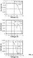
- Fig. 5 shows a current and voltage function (IV curve) of a multijunction solar cell according to the present disclosure at 15.5 suns compared to current and voltage functions of two exemplary prior art multijunction solar cells at 1.2 and 1.4 suns using homojunction AlGaInAs/AlGaInAs tunnel diode.
- the solar cell using a type II tunnel diode as described in this disclosure provides an IV curve functioning as intended at 15.5 suns, and having a peak tunneling current exceeding the current required to operate the solar cell, which is capable of handling current density of 0.25A/cm 2 at this concentration.
Landscapes
- Engineering & Computer Science (AREA)
- Power Engineering (AREA)
- Microelectronics & Electronic Packaging (AREA)
- Life Sciences & Earth Sciences (AREA)
- Electromagnetism (AREA)
- Computer Hardware Design (AREA)
- Physics & Mathematics (AREA)
- Condensed Matter Physics & Semiconductors (AREA)
- General Physics & Mathematics (AREA)
- Chemical & Material Sciences (AREA)
- Sustainable Development (AREA)
- Sustainable Energy (AREA)
- Crystallography & Structural Chemistry (AREA)
- Inorganic Chemistry (AREA)
- Manufacturing & Machinery (AREA)
- Photovoltaic Devices (AREA)
Description
- The present disclosure generally relates to photovoltaic cells and, more specifically, to solar cells of InP lattice constant having high bandgap, type-II tunnel junctions.
- A solar cell is a device that is capable of converting sunlight energy to electricity by photovoltaic effect. A solar cell can have one or more photovoltaic subcells or p-n junctions. A multijunction solar cell has more than one photovoltaic subcells that are monolithically connected in series.
- The interest in solar cells has been increasing due to concerns regarding pollution and limited available resources. This interest has been for both terrestrial and space applications. In space applications, solar cells have been in use for more than 40 years and the development of higher efficiency solar cells enables increased payload capabilities.
- The relatively high cost per watt of electrical power generated by photovoltaic systems inhibits their widespread use in terrestrial applications. The conversion efficiency of sunlight to electricity may be critically important for terrestrial PV systems, since increased efficiency usually results in a reduction of related electricity generation system components (such as cell area, module or collector area, support structures, and land area) for a required power output of the system. For example, in concentrator solar cell systems which concentrate sunlight from around 2 to around 2000 times onto the solar cell, an increase in cell efficiency typically results in a reduction of an area comprising expensive solar cells and concentrating optics. Improvements in solar cell efficiency are extremely leveraging at the system level, and the dollar per watt ($/watt) is a typical figure-of-merit applied at the system level. For satellites, solar panels represent <10% of the entire system cost so that a relative improvement in solar cell efficiency of 3% over an existing technology generation results in cost savings. The same is true of terrestrial concentrator solar power systems where the cost of the solar receiver is a small fraction of the overall system cost.
- To increase the electrical power output of such solar cells, multiple subcells or layers having different energy bandgaps have been stacked so that each subcell or layer can absorb a different part of the wide energy distribution in the sunlight. This arrangement is advantageous, since each photon absorbed in a subcell corresponds to one unit of charge that is collected at the subcell operating voltage, which is approximately linearly dependent upon the band gap of the semiconductor material of the subcell. Since the output power is the product of voltage and current, an ideally efficient solar cell would have a large number of subcells, each absorbing only photons of energy negligibly greater than its band gap.
- Lattice constants of compounds and alloys used to form photovoltaic cells are well known. When such materials are combined into devices having subcells of different materials, it is important that the lattice of the different materials have the same lattice constants to within a small difference. This avoids the formation of imperfections in the crystalline structures that can drastically lower the efficiency of the devices. When the term lattice-matched is used herein, it denotes a difference in lattice constants of the materials of not more than about 0.3 percent. Preferably, lattice constants are matched to within about 0.2 percent or less.
- In any multijunction device, electrical connection must be made between the subcells. Preferably, these intercell ohmic contacts (IOCs) should cause very low loss of transmitted light between cells. Therefore, these contacts should have maximum optical transparency and minimal electrical resistance. There are two methods known for making such IOCs, metal interconnects and tunnel junctions (or tunnel diodes). Metal interconnects can provide low electrical resistance, but they are poor in optical transparency and difficult to fabricate. Complex processing of metal interconnects results in substantial loss in the device efficiency and reliability. Therefore, tunnel junctions are much preferred. A monolithic integrated device can be produced having a plurality of subcells with tunnel junctions therebetween. But the tunnel junctions must satisfy multiple requirements, such as low resistivity, low optical losses, and crystallographic compatibility through lattice-matching between contacting subcells. Most importantly, they must exhibit a high peak current density.
- One type of tunnel junction that has been used in multijunction solar cells lattice-matched to InP lattice constant is a highly doped AlGaInAs homojunction based tunnel diode. A homojunction is a semiconductor interface that is between two similar layers that have the same bandgap, but different type of doping, in this case, the interface between a n-doped AlGaInAs and a p-doped AlGaInAs layers.
-
Fig. 1 illustrates a prior art InP-based dual-junctionsolar cell 100, hereinafter referred to as the "prior art cell" 100. As can be seen inFig. 1 , theprior art cell 100 includes afirst subcell 102 and asecond subcell 104. Thefirst subcell 102 includes a first GaInPAs emitter andbase 120. Thefirst subcell 102 further includes awindow layer 110 deposited atop the first GaInPAs emitter andbase 120, and a p-doped InP back-surface field (BSF)layer 130 disposed on the opposite side (or bottom) of the first GaInPAs emitter andbase 120. Thesecond subcell 104 includes a second GaInPAs emitter andbase 170, having a n-dopedInP window 160 disposed a top thereof, and aBSF layer 180 disposed on the opposite side (or bottom) thereof. The first and second GaInPAs emitter and base, 120, 170 have bandgap energies of 1.1 electron volts (eV) and 0.8 eV, respectively. Between the first andsecond subcells tunnel diode 190. The AlGaInAs homojunction basedtunnel junction 190 includes a n-doped AIGaInAstunnel layer 150 and a p-doped AlGaInAstunnel layer 140. - Other types of tunnel junctions that have been used in multijunction solar cell lattice-matched to InP lattice constant include type-II, low bandgap GaInAs/GaAsSb tunnel diodes, lattice-mismatched AlGaInAs/AlGaAs, and lattice-mismatched AlGalnAs/GaAs tunnel diodes. However, the low bandgap, type-II tunnel junction reduces the amount of light available to the second subcell leading to lower conversion efficiency. Additionally, the arsenide-based, lattice-mismatched AlGaInAs/AlGaAs and AlGaInAs/GaAs tunnel-diodes involve lattice-mismatch material and may require strain balancing, which add complications during growth and often degrade the performance of the photovoltaic subcells. Furthermore, the repeatability of the lattice-mismatched material approaches has been poor and maintaining good material quality has been difficult.
- There exists a need for a tunnel junction of InP lattice constant that provides for improved peak tunneling current with low optical and electrical losses. Such tunnel junctions enable multijunction solar cells to operate at higher solar intensity without compromising overall device performance that can leads to higher power conversion efficiency.
- A solar cell is e.g. known from the paper "High efficiency InP based four-junction solar cells", Gu et al., LEOS 2003, 16th. annual Meeting of the IEEE Lasers & Electro-optics society, Tuscon, AZ, Oct. 27-28, 2003, New York, IEEE, US vol. 2, 26 October 2003, pages 927-028.
- In the paper Yonglin Gu: "DESIGN, FABRICATION AND CHARACTERIZATION OF HETERO-PN-JUNCTION DEVICES FOR PHOTOVOLTAIC AND PHOTODETECTION APPLICATIONS", Dissertation, 2008, XP055186121, University of Maryland, devices for photovoltaic and photodetection applications are discussed.
-
US 2007/0127533 A1 according to its abstract states: Disclosed herein is a vertical cavity surface emitting laser device. The laser device comprises a semiconductor lower mirror layer, a first semiconductor electrode layer, a gain-activation layer and a semiconductor anode layer sequentially grown on the compound semiconductor substrate, a re-growth pattern formed on the semiconductor anode layer to a width of 10-100 um and an etching depth equal to or less than the semiconductor anode layer by etching, a first anode semiconductor buffer layer grown at a low temperature on the pattern, a second anode semiconductor layer grown at the low temperature for formation of an oxide layer, an anode semiconductor layer for tunnel junction, a cathode semiconductor layer for tunnel junction, a second semiconductor electrode layer for injection of electrons, and an upper mirror layer formed on the second semiconductor electrode layer. With this structure, the laser device comprises an effective electric current confining structure. -
US 2009/0014712 A1 according to its abstract states: A tunnel junction light emitting device according to the present invention is provided with an active layer and an electron tunneling region supplying the active layer with carriers. The electron tunneling region has a first p-type semiconductor layer, a second p-type semiconductor layer and an n-type semiconductor layer. The second p-type semiconductor layer is sandwiched between the first p-type semiconductor layer and the n-type semiconductor layer, and the first p-type semiconductor layer, the second p-type semiconductor layer and the n-type semiconductor layer form a tunnel junction to which a reverse bias is applied. An energy level at a valence band edge of the second p-type semiconductor layer is equal to or lower than an energy level at a valence band edge of the first p-type semiconductor layer. -
US 5,679,963 according to its abstract states: The incorporation of a pseudomorphic GaAsSb layer in a runnel diode structure affords a new degree of freedom in designing runnel junctions for p-n junction device interconnects. Previously only doping levels could be varied to control the tunneling properties. This invention uses the valence band alignment band of the GaAsSb with respect to the surrounding materials to greatly relax the doping requirements for tunneling. -
GB 2 255 227 A - The present invention provides an improved photovoltaic device as defined in
claim 1 having type-II, high bandgap tunnel junction of InP lattice constant for solar (photovoltaic) cell that is most preferably utilized in a multijunction structure. The disclosed type-II, high bandgap tunnel junction enables solar cells to achieve increased efficiency and performance, with little change in cost, as compared with conventional solar cells. - In accordance with the disclosure, a high bandgap, type-II tunnel junction is disclosed that includes a p-doped AlGaInAs tunnel layer and a n-doped InP tunnel layer.
- In accordance with the disclosure, a multijunction solar cell of InP lattice constant is disclosed that includes a high-bandgap, type-II tunnel junction. The high bandgap type-II tunnel junction includes a p-doped AlGaInAs tunnel layer, and a n-doped InP tunnel layer.
- In accordance with the disclosure, a method of forming a tunnel junction is disclosed that includes growing AlGaInAs and InP doped tunnel layers in a Metalorganic Vapor Phase Epitaxy (MOVPE) reactor to form a type-II high bandgap tunnel junction. One advantage of the present disclosure is providing for a tunnel junction having increased tunneling current through the p-n junction.
- Another advantage of the present disclosure is providing for a tunnel junction having a narrower space charge region, increasing the tunneling probability and increasing the peak tunneling current of the tunnel-diode for handling higher solar intensity.
- Another advantage of the present disclosure is providing for a tunnel junction having an improved material growth process.
- Another advantage of the present disclosure is providing for a tunnel junction having a higher bandgap than existing homojunction-based tunnel diode and type II GaAsSb/GaInAs tunnel junctions.
- Another advantage of the present disclosure is providing for a tunnel junction having higher optical transparency (λ>920nm) than existing tunnel junctions, thus reducing optical parasitic loss.
- Another advantage of the present disclosure is providing for a single bandgap binary semiconductor layer acting as both a window, a BSF, and a tunnel junction layer by changing the corresponding doping polarity and doping levels. This reduces the complexity of the cell structure design and the corresponding MOVPE growth process.
- A method of making a photovoltaic device is defined in claim 11.
- Other features and advantages of the present disclosure will be apparent from the following more detailed description of the preferred embodiment, taken in conjunction with the accompanying drawings, which illustrate, by way of example, the principles of the disclosure.
-
-
Fig. 1 illustrates a prior art InP-based dual-junction solar cell. -
Fig. 2 illustrates an exemplary embodiment of a solar cell according to the disclosure. -
Fig. 3 illustrates the staggered bandgap alignment of n-doped InP layer and p-doped AlGaInAs layers of a type II heterojunction as formed by the tunnel junction of the present disclosure. -
Fig. 4 illustrates an InP-based triple junction solar cell using high bandgap, Type-II tunnel junctions according to the present disclosure. -
Fig. 5 shows a chart of the relationship between current and voltage of a multijunction solar cell of the present disclosure at 15.5 suns compared to prior art multijunction solar cells at 1.2 and 1.4 suns. - Wherever possible, the same reference numbers will be used throughout the drawings to represent the same parts.
-
Fig. 2 illustrates adevice 200 according to an embodiment of the disclosure. Thedevice 200 is a photonic device. In this embodiment, thedevice 200 is a solar cell. In another embodiment, thedevice 200 may be a multijunction solar cell. In another embodiment, thedevice 200 may be other photonic devices such as laser power converter or sensors for converting light to electricity. Both solar cells, which convert a broad spectrum of light power to electrical power, as well as laser power converters which convert light at a single wavelength to electrical power, are examples of photonic devices that benefit from improved tunnel junction performance. - As can be seen in
Fig. 2 , thedevice 200 is an InP-based dual-junction solar cell, meaning it includes two photovoltaic cells. The individual photovoltaic cells may be referred to as subcells. Thedevice 200 includes a firstphotovoltaic cell 202 and a secondphotovoltaic cell 204. The firstphotovoltaic cell 202 includes a first emitter andbase 220. In this exemplary embodiment, the first emitter andbase 220 is a GaInPAs emitter and base having an InP lattice constant. In another embodiment, the first emitter andbase 220 may be III-V material such as, but not limited to AlAsSb, AlGaAsSb, AlInAs, InP, AlGaInAs, GaInAs, GaAsSb or GaInPAs with different bandgaps having lattice constant same as InP. In one embodiment, the first emitter andbase 220 includes a separate emitter layer and base layer (not shown), the emitter layer being nearest incident light. - The first
photovoltaic cell 202 has a bandgap of 1.1 eV. In another embodiment, the firstphotovoltaic cell 202 may have a bandgap of from about 0.73 to 2.45 eV. In another embodiment, the firstphotovoltaic cell 202 may have a bandgap of from about 1.0 to 1.1 eV. In yet another embodiment, the firstphotovoltaic cell 202 may have a bandgap of from about 1.0 to 1.1 eV and may be included in a three or more-junction solar cell. The firstphotovoltaic cell 202 is sensitive to a first-photoactive-subcell-layer wavelength. As used herein, "wavelength" may mean a single discrete wavelength, or, "wavelength" may include a range of wavelengths at which the layer material achieves a good light-to-electricity conversion efficiency. - The first
photovoltaic cell 202 further includes awindow layer 210. Thewindow layer 210 is disposed on afirst side 220a of the first emitter andbase 220, which would be positioned nearest to incident light, which is represented by arrow L. As used herein, the relative terms "top" and "bottom" are used to indicate the surface nearest to and farthest from incident light, respectively. Also, when used to compare two layers, "upper" or "above" or "overlying" refers to a layer closer to the sun, and "lower" or "below" or "underlying" refers to a layer further from the sun or other source of illumination. Thewindow layer 210 may be InP, AlGaInAs, AlInAs, AlAsSb, AlGaAsSb, GaInPAs composition that provides bandgap energy greater than about 1.1 eV. Thewindow layer 210 has two functions. The first function of thewindow layer 210 is to reduce minority-carrier recombination (i.e., to passivate) on thefront surface 220a of the firstphotovoltaic subcell 202. Additionally, the optical properties of the window material must be such that as much light as possible is transmitted to the firstphotoactive subcell 202, and any additional photoactive subcell layers that may be disposed underneath thereof (not shown), where the photogenerated charge carriers can be collected more efficiently. If there is substantial light absorption in thewindow layer 210, carriers generated in the window layer are less likely to be subsequently collected and hence light absorption in the window degrades overall conversion efficiency. - The
device 200 may optionally include an antireflection (AR) layer or coating (not shown) disposed on top of thedevice 200 nearest incident light L, which is shown impinging from the direction indicated by the arrows. In one embodiment, the AR coating may be disposed atop thewindow layer 210. The AR coating is intended to minimize surface reflections between the optically transparent media above the cell (such as air, glass, or polymer) and the semiconductor layers of thedevice 200, thereby enabling more photons to enter thedevice 200. The AR coating may be made from well-known materials in the art, such as TiO2, Ta2O5, SiO2, and MgF2. The thickness of the AR coating may vary, but is typically between about 0.04 and 0.35 microns. While an AR coating can be applied todevice 200, in other configurations another subcell can be stacked or applied above thedevice 200 with another tunnel junction therebetween. - The first
photovoltaic cell 202 further includes a p-dopedBSF layer 230 disposed on the bottom of first emitter andbase 220. In this exemplary embodiment, the p-dopedBSF layer 230 is a p-doped InP BSF layer. In another embodiment, the p-dopedBSF layer 230 may be AlGaInAs, GaAsSb, AlAsSb, AlGaAsSb, AlInAs, GaInPAs and their alloys layer. In one embodiment, theBSF layer 230 is lattice-matched to InP. In another embodiment, theBSF layer 230 may be a coherently strained layer with a thickness below the Matthews-Blakeslee thickness. The p-dopedBSF layer 230 reduces minority-carrier recombination at the back surface of the first emitter andbase 220. The p-dopedBSF layer 230 has optical properties that allow light that can be used by subcells beneath the p-dopedBSF layer 230 to be transmitted through the p-dopedBSF layer 230, and/or the minority-carrier properties in the p-dopedBSF layer 230 must be such that electrons and holes that are generated by light absorption in the p-dopedBSF layer 230 are efficiently collected at the p-n junction of thedevice 200. Minority carrier electrons are collected at thep-n junction 290 of first emitter andbase 220. The p-doping in theBSF layer 230 and first emitter andbase 220 are typically graded from highest concentration at theBSF layer 230 to lowest concentration at a base layer (not shown) of the first emitter andbase 220 to create an electric field that sweeps electrons from theBSF layer 230 towards the emitter andbase 220. - The second
photovoltaic cell 204 includes a second emitter andbase 270. In this exemplary embodiment, the second emitter andbase 270 is a GaInPAs layer having an InP lattice constant. In another embodiment, the second emitter andbase 270 may be GaInAs, GaAsSb, AlGaInAs, AlGaAsSb, GaInPAs and their alloys having an InP lattice constant. The second emitter andbase 270 has a bandgap lower than the bandgap of the first emitter andbase 220. - In this exemplary embodiment, the second
photovoltaic cell 204 has a bandgap of about 0.8 eV. In another embodiment, the secondphotovoltaic cell 204 may have a bandgap of from about 0.73 to 2.0 eV. In another embodiment, the secondphotovoltaic cell 204 may have a bandgap of from about 0.73 to 0.8 eV. In yet another embodiment, the secondphotovoltaic cell 204 may have a bandgap of from about 0.73 to 0.8 eV and be included in a three or more-junction solar cell lattice matched to InP. - The second
photovoltaic cell 204 further includes an n-dopedwindow layer 260 disposed on top of the second emitter andbase 270. The general characteristics of the n-dopedwindow layer 260 is similar to the window characteristics of thewindow layer 210. The n-dopedwindow 260 has an n-doping concentration of between about 2×10¹⁸/cm3 and 2×10¹⁹/cm3. In another embodiment, the n-dopedwindow 260 has a n-doping concentration of about 1×10¹⁹/cm3 to create a large electric field and passivated thep-n junction 270. - The second
photovoltaic cell 204 further includes a second back-surface field (BSF)layer 280 below the second emitter andbase 270. In one embodiment, thesecond BSF layer 280 may be an InP, AlGaInAs, AlAsSb, GaAsSb, AlGaAsSb, or GaInPAs wider bandgap layer. In one embodiment, thesecond BSF layer 280 is lattice-matched to InP. In another embodiment, theBSF layer 280 may be a coherently strained layer with a thickness below the Matthews-Blakeslee thickness. Thesecond BSF layer 280 provides a passivation function similar to thewindow layer 210, and has BSF characteristics similar to those of the p-dopedInP BSF layer 230. As such, thesecond BSF layer 280 reduces minority-carrier recombination at theback surface 270b of the second emitter andbase 270. Thesecond BSF layer 280 must also have optical properties that allow most of the light that can be used by any subcells beneath the second BSF layer to be transmitted through the second BSF layer, and/or the minority-carrier properties in thesecond BSF layer 280 must be such that electrons and holes which are generated by light absorption in thesecond BSF layer 280 are efficiently collected in thecell 204. - The
device 200 further includes a highly doped, high band-gap, type-II tunnel junction, which may be referred to as tunnel junction orp-n junction 290. The p-n junction has an InP lattice constant connecting the firstphotovoltaic cell 202 and the secondphotovoltaic cell 204 in electrical series. The type-II indicates that more favorable band alignment is provided that charged particles can tunnel through the p-n junction with less energy. This results in a narrower space charge region increasing the tunneling probability and increasing the peak tunneling current of the tunnel-diode for handling higher solar intensity. The purpose of doping thep-n junction 290 at high levels is to reduce the resistance for charged carriers to tunnel through thep-n junction 290. - The
p-n junction 290 includes a highly p-dopedtunnel layer 240 and a highly n-dopedtunnel layer 250. The highly p-dopedtunnel layer 240 is lattice matched to InP. The doping level ranges from 1×10¹⁹/cm3 to 1×10²⁰/cm3 for these tunnel layers. In one embodiment, the n-dopedInP tunnel layer 250 may serve as tunnel layer for tunnel diode as well as a window layer for subcell underneath the tunnel diode. - According to the invention, the highly p-doped
tunnel layer 240 is a highly p-doped AlGaInAs tunnel layer. In another embodiment, the highly p-dopedtunnel layer 240 is AlxGal-xInAs with x > 0.25 up to x=1. The highly p-dopedtunnel layer 240 has a bandgap of greater than or equal to 1.25 eV. In one embodiment, the highly p-dopedtunnel layer 240 has a bandgap greater than 1.25 eV. In another embodiment, the highly p-dopedtunnel layer 240 has a bandgap of 1.45 eV. - The highly n-doped
tunnel layer 250 is lattice matched to InP. In an embodiment, the highly n-dopedtunnel layer 250 is high bandgap III-V semiconductor having a InP lattice constant and that can form type II band alignment with the p-doped tunnel layer. According to the invention, the highly n-doped tunnel layer is a highly n-doped AlInPAs, AlAsSb, or AlInAsSb tunnel layer having a bandgap greater than or equal to 1.35 eV and an InP lattice constant. In one embodiment, not covered by the claimed invention, the highly n-dopedInP tunnel layer 250 is an InP tunnel layer having a bandgap of 1.35 eV. - The bandgap of the highly p-doped
tunnel layer 240 must be equal to or greater than 1.25 eV to form a type-II staggered tunnel-junction with the highly n-dopedtunnel layer 250. For a higher bandgap, n-doped tunnel layer of AlInPAs, a p-doped tunnel layer of AlInAs may be used. The bandgap difference or Al-composition difference must be maintained to form a type-II staggered tunnel diode. - The
solar cell 200 may further include a substrate (not shown) beneath theBSF layer 280. In one embodiment, the substrate may be InP. In another embodiment, the substrate may be silicon, GaSb, CdTe, InP/Si template or InGaAs/Si template or other semiconductor. In an embodiment, the substrate may be single side polished or double side polished. In an embodiment, the substrate may have a surface orientation of (100) and thickness of 300-1000 µm or beyond. In an embodiment, the substrate may be doped either n-type or p-type. In an embodiment, the substrate is doped p-type. In one embodiment, the substrate may be doped to greater than 5×10¹⁸ /cm3 to enable ohmic contact to a metal contact layer. -
Window layer 210 may have a heavily doped n-type cap layer above it that is patterned using standard photolithographic techniques. This pattern is designed to leave large areas of the window layer open to incident light. This cap layer may have a metal contact layer patterned to make contact to only the cap layer, leaving large areas of the window open to incident light. The metal contact layer enables ohmic contact to be made to the solar cell for subsequent assembly into a power providing electrical circuit. - The
p-n junction 290 provides improved optical transparency and improved peak tunneling current in the tunnel junction ofdevice 200 without compromising overall device performance, which leads to higher power conversion efficiency at higher solar intensity. Thep-n junction 290 is capable of performing at higher solar intensity, consequently improving higher solar energy conversion efficiency. - The AlGaInAs and InP doped tunnel layers 240, 250 are grown sequentially in a Metalorganic Vapor Phase Epitaxy (MOVPE) reactor to form the
p-n junction 290, in this case a tunnel junction diode. Furthermore, thedevice 200 and device components (window, BSF) are be grown in a MOVPE reactor. In another embodiment, thep-n junction 290 may be grown in a Metalorganic Vapor Phase Epitaxy (MOVPE), Molecular Beam Epitaxy (MBE), Chemical Beam Epitaxy (CBE), Hydride Vapor Phase Epitaxy (HVPE) or Atomic Layer Deposition (ALD) reactor. - The
device 200 shown inFig. 2 is an upright solar cell configuration, or in other words, thedevice 200 is grown with new layers above the prior layer and with the highest bandgap cell of multi-junction cells last. In another embodiment, thedevice 200 may be inverted or with the highest bandgap cell of multi-junction cells grown first. The growth sequence changes depending on upright or inverted configuration, however for testing and field operations, the highest bandgap cell is sitting closest to the sun. In an embodiment, thedevice 200 may be an inverted InP-based multijunction cell with a high bandgap, type-II tunnel junction. According to the disclosure, a p-doped tunnel layer is always between a p-doped BSF layer and n-doped tunnel layer and n-doped tunnel layer is between p-doped tunnel layer and n-doped window layer. - According to the present disclosure, the bandgap of the material (AlGaInAs/InP) in the
tunnel junction 290 is higher than existing solutions, for example when compared to a tunnel junction of GaInAs/GaAsSb having a bandgap of 0.73/0.77 eV respectively, which allows higher optical transparency for lower parasitic loss. The present disclosure provides for ap-n junction 290 having a bandgap of AlGaInAs of 1.25 eV and bandgap of InP is 1.35 eV, as compared to an AlGaInAs homojunction based tunnel diode of the prior art having bandgap of 1.25 eV across the diode. In one embodiment, the bandgap of thetunnel junction 290 ranges from 0.73 eV to 2.0 eV, lattice matched to InP lattice constants. In another embodiment, the band gap of thetunnel junction 290 is greater than 1.25 eV. In one embodiment, thetunnel junction 290 has a greater optical transparency (λ) than existing solutions. - Other embodiments utilizing even higher bandgap semiconductor alloys, e.g. AlInAs, AlAsSb, and AlInPAs may have even greater optical transparency for an extended wavelength range. The band offset of the material used (such as, AlGaInAs/InP) in the
tunnel junction 290 forms a type II heterostructures tunnel junction diode that reduces the amount of energy required for charged particles to tunnel through the p-n junction. This results in a narrower space charge region increasing the tunneling probability and increasing the peak tunneling current of the tunnel-diode for handling higher solar intensity. - A heterojunction based tunnel diode places an alloy layer in a region of the device (the n-region of a p-n junction) that forms Type-II band alignment with the p-region of a tunnel junction. In general, the tunneling probability can be approximated by the following equation:

- Where Eg is the bandgap of the junction semiconductor layer and w is the depletion width of the p-n junction.
- The equation indicates that tunneling probability increases as the bandgap of the junction decreases. In a type II heterojunction as formed by the
p-n junction 290, the bandgap of n-doped layer and p-doped layer staggers as shown inFig. 3 . This band alignment reduces Eg to Eg eff, the energy gap to be between the valance band edge of the p-side and the conduction band edge of the n-side at the heterojunction interface. Since Eg eff is smaller than Eg of the homojunction, the tunneling probability of the type II tunnel junction does get higher than that of the homojunction. - The
p-n junction 290, which may be referred to as high bandgap, type-II tunnel junction diode, may monolithically integrate photovoltaic subcells formed of InP, AlInAs, AlInAsP, AlAsSb, AlInAsSb, AlGaAsSb, AlGaInAs, GaInPAs, GaInAs, GaAsSb and their combination into a multijunction solar cell of InP lattice constant. In one embodiment, the high bandgap (e.g. AlGaInAs/InP) type-II tunnel junction diode may enable a single junction solar cell to be grown onto a substrate of opposite polarity than the first layer (such as p-type BSF or n-type window) of the intended devices for use in a space or terrestrial applications. - In addition, the AlGaInAs/InP type-II tunnel junction diode may enable the fabrication of ultra-high efficiency (>33%) direct-semiconductor bonded multijunction solar cells, Carbon NanoTube-bonded (CNT-bonded) multijunction solar cells, and multijunction solar cells with component subcells at the InP lattice-constant. For example, low bandgap (~0.7-1.2-eV) component subcells at the InP lattice constant are becoming one of the key component in the ultra-high efficiency (>33%) multijunction solar cell structure.
- In another embodiment, the AlGaInAs/InP type-II tunnel junction diode may be used in a multijunction solar cell, resulting in a solar cell of desirable bandgap combinations with higher performance due to the higher peak tunneling current and lower parasitic optical loss.
-
Fig. 4 illustrates an embodiment of a multijunctionphotovoltaic device 400. Thephotovoltaic device 400 may be a multijunction solar cell As can be seen inFig. 4 , a multijunctionsolar cell 400 is shown that includes a firstphotovoltaic cell 410, a secondphotovoltaic cell 420, and a thirdphotovoltaic cell 430. Disposed between the adjacent cells arep-n junctions 290 as described above. - The multijunction
solar cell 400 further includes asubstrate 450. In this exemplary embodiment, thesubstrate 450 is an InP substrate. In another embodiment, thesubstrate 450 may be InP layer or III-V semiconductor layer with an InP lattice constant transferred onto virtual substrates, such as hybrid templates in a combination of InP or GaInAs with Si, Ge, GaAs, InAs, GaP, GaSb, polymer, metal substrate. Furthermore, the multijunctionsolar cell 400 may further include window and BSF layers as described above. -
Fig. 5 shows a current and voltage function (IV curve) of a multijunction solar cell according to the present disclosure at 15.5 suns compared to current and voltage functions of two exemplary prior art multijunction solar cells at 1.2 and 1.4 suns using homojunction AlGaInAs/AlGaInAs tunnel diode. As can be seen inFig. 5 , the solar cell using a type II tunnel diode as described in this disclosure provides an IV curve functioning as intended at 15.5 suns, and having a peak tunneling current exceeding the current required to operate the solar cell, which is capable of handling current density of 0.25A/cm2 at this concentration. - Although a particular embodiment of the disclosure has been described in detail for purposes of illustration, various modifications and enhancements may be made without departing from the scope of the appended claims.
Claims (15)
- A photovoltaic device (200), comprising:a high bandgap, type-II tunnel junction (290) comprising:a p-doped tunnel layer; anda n-doped tunnel layer in contact with the p-doped tunnel layer;wherein the tunnel junction has an InP lattice constant, wherein the p-doped tunnel layer is a p-doped material of AlGaInAs;wherein the high bandgap, type II tunnel junction forms a type II heterojunction; andthe n-doped tunnel layer is a n-doped material selected from the group consisting of AlAsSb, AlInAsSb, and AlInPAs;wherein the p-doped tunnel layer has a bandgap of greater than or equal to 1.25 eV and the n-doped tunnel layer has a bandgap of greater than or equal to 1.35 eV;
andwherein the p-doped tunnel layer and the n-doped tunnel layer have
a doping level between from 1×10¹⁹/cm3 to 1×10²⁰/cm3;a first photovoltaic cell (202) disposed on a first side of the type-II tunnel junction (290); anda second photovoltaic cell (204) disposed on a second side of the type-II tunnel junction (290). - The photovoltaic device of claim 1, wherein the p-doped tunnel layer is a p-doped material selected from the group consisting of AlxGa1-xInAs with x greater than or equal to 0.25 up to x=1; and the n-doped tunnel layer is a n-doped material selected from the group consisting of AlAsSb, AlInAsSb, AlInPAs.
- The photovoltaic device of claim 2, further comprising:
one or more additional photovoltaic cells in electrical connectivity with the first and second photovoltaic cells. - The photovoltaic device of claim 2 or 3 wherein the first photovoltaic cell (202) and the second photovoltaic cell (204) are selected from the group consisting of InP, AlInAs, AlAsSb, AlInAsSb, AlInPAs, AlGaInAs, GaInPAs, GaInAs, AlGaAsSb, GaAsSb, and their combinations.
- The photovoltaic device of any of claims 3 or 4, wherein the one or more additional photovoltaic subcells have the high bandgap, type-II tunnel junction disposed therebetween.
- The photovoltaic device of claim 1, wherein the first photovoltaic cell (202) includes a first emitter and base (220).
- The photovoltaic device of claim 6, wherein the first photovoltaic cell (202) includes a window layer (210) disposed on a first side (220a) of the first emitter and base (220).
- The photovoltaic device of claim 7, wherein the device (200) includes an antireflection (AR) layer disposed atop the window layer (210).
- The photovoltaic device of claim 8, wherein the first photovoltaic cell (202) includes a p-doped back-surface field, BSF, layer (230) disposed on the bottom of first emitter and base (220).
- The photovoltaic device of claim 9, wherein the second photovoltaic cell (204) includes a second emitter and base (270).
- A method of making a photovoltaic device, comprising:growing a p-doped tunnel layer; andgrowing a n-doped tunnel layer;wherein the p-doped and n-doped tunnel layers form a high bandgap, type-II tunnel junction having an InP lattice constant,wherein the p-doped tunnel layer is a p-doped material of AlGaInAs, and the n-doped tunnel layer is a n-doped material selected from the group consisting of AlAsSb, AlInAsSb, and AlInPAs,wherein the tunnel junction forms a type II heterojunction;wherein the p-doped tunnel layer has a bandgap of greater than or equal to 1.25 eV and the n-doped tunnel layer has a bandgap of greater than or equal to 1.35 eV; andwherein the p-doped tunnel layer and the n-doped tunnel layer have a doping level between from 1×10¹⁹/cm3 to 1×10²⁰/cm3; anddisposing a first photovoltaic cell (202) on a first side of the type-II tunnel junction (290); and a second photovoltaic cell (204) on a second side of the type-II tunnel junction (290).
- The method of claim 11, further comprising:
growing two or more photovoltaic cells separated by the high bandgap, type-II tunnel junction. - The method of claim 11, wherein the p-doped tunnel layer is a p-doped material selected from the group consisting of AlxGa1-xInAs with x greater than or equal to 0.25 up to x=1; and the n-doped tunnel layer is a n-doped material selected from the group consisting of AlAsSb, AlInAsSb, AlInPAs.
- The method of claim 12 or 13 wherein the first photovoltaic cell (202) and the second photovoltaic cell (204) are selected from the group consisting of InP, Alln-As, AlAsSb, AlInAsSb, AlInPAs, AlGaInAs, GaInPAs, GaInAs, AlGaAsSb, GaAsSb, and their combinations.
- The method of claim 11, wherein the high bandgap, type II tunnel junction is formed in a Metalorganic Vapor Phase Epitaxy, MOVPE, reactor.
Applications Claiming Priority (2)
| Application Number | Priority Date | Filing Date | Title |
|---|---|---|---|
| US12/950,912 US11417788B2 (en) | 2010-11-19 | 2010-11-19 | Type-II high bandgap tunnel junctions of InP lattice constant for multijunction solar cells |
| PCT/US2011/052898 WO2012067715A2 (en) | 2010-11-19 | 2011-09-23 | TYPE-II HIGH BANDGAP TUNNEL JUNCTIONS OF InP LATTICE CONSTANT FOR MULTIJUNCTION SOLAR CELLS |
Publications (2)
| Publication Number | Publication Date |
|---|---|
| EP2641275A2 EP2641275A2 (en) | 2013-09-25 |
| EP2641275B1 true EP2641275B1 (en) | 2022-07-06 |
Family
ID=44721114
Family Applications (1)
| Application Number | Title | Priority Date | Filing Date |
|---|---|---|---|
| EP11764066.4A Active EP2641275B1 (en) | 2010-11-19 | 2011-09-23 | TYPE-II HIGH BANDGAP TUNNEL JUNCTIONS OF InP LATTICE CONSTANT FOR MULTIJUNCTION SOLAR CELLS |
Country Status (7)
| Country | Link |
|---|---|
| US (1) | US11417788B2 (en) |
| EP (1) | EP2641275B1 (en) |
| JP (1) | JP2013543278A (en) |
| KR (1) | KR101908742B1 (en) |
| CN (2) | CN107863400A (en) |
| CA (1) | CA2810895C (en) |
| WO (1) | WO2012067715A2 (en) |
Families Citing this family (21)
| Publication number | Priority date | Publication date | Assignee | Title |
|---|---|---|---|---|
| US10283658B2 (en) * | 2011-02-09 | 2019-05-07 | The Board Of Regents Of The University Of Oklahoma | Interband cascade devices |
| CN102751367A (en) * | 2012-07-10 | 2012-10-24 | 厦门市三安光电科技有限公司 | Triple-junction solar battery and preparation method thereof |
| GB2504977B (en) * | 2012-08-16 | 2017-10-04 | Airbus Defence & Space Gmbh | Laser power converter |
| CN102832274B (en) * | 2012-09-05 | 2015-01-07 | 天津三安光电有限公司 | Flip-chip solar cell and manufacture method thereof |
| JP2015038952A (en) * | 2013-07-16 | 2015-02-26 | 株式会社リコー | Compound semiconductor solar cell and compound semiconductor solar cell manufacturing method |
| EP2973745B1 (en) * | 2013-03-14 | 2021-04-28 | Ricoh Company, Ltd. | Compound semiconductor photovoltaic cell and manufacturing method of the same |
| JP6446782B2 (en) * | 2013-03-14 | 2019-01-09 | 株式会社リコー | Compound semiconductor solar cell and method of manufacturing compound semiconductor solar cell |
| JP6550691B2 (en) | 2013-07-30 | 2019-07-31 | 株式会社リコー | Compound semiconductor solar cell |
| JP6582591B2 (en) * | 2014-07-11 | 2019-10-02 | 株式会社リコー | Compound semiconductor solar cell and method of manufacturing compound semiconductor solar cell |
| JP2016122752A (en) * | 2014-12-25 | 2016-07-07 | 国立大学法人 東京大学 | Solar battery |
| DE102015006379B4 (en) * | 2015-05-18 | 2022-03-17 | Azur Space Solar Power Gmbh | Scalable voltage source |
| US20170084771A1 (en) * | 2015-09-21 | 2017-03-23 | The Boeing Company | Antimonide-based high bandgap tunnel junction for semiconductor devices |
| US10784396B2 (en) * | 2015-09-30 | 2020-09-22 | Panasonic Intellectual Property Management Co., Ltd. | Solar cell, solar cell module, and production method for solar cell |
| US10923610B2 (en) | 2015-09-30 | 2021-02-16 | Panasonic Intellectual Property Management Co., Ltd. | Solar cell and solar cell module |
| MD4510C1 (en) * | 2016-06-23 | 2018-03-31 | Государственный Университет Молд0 | Method for growth of n+-p-p+ InP structure for solar cells |
| TWI601298B (en) * | 2017-02-10 | 2017-10-01 | 友達光電股份有限公司 | Photovoltaic device |
| DE102017005950A1 (en) * | 2017-06-21 | 2018-12-27 | Azur Space Solar Power Gmbh | solar cell stack |
| KR101829743B1 (en) | 2017-08-29 | 2018-02-20 | 아이피랩 주식회사 | Three-dimensional lattice structure for tailoring the band gaps |
| MD4554C1 (en) * | 2017-10-18 | 2018-09-30 | Государственный Университет Молд0 | Process for increasing the efficiency of photovoltaic cells based on p+InP-p-InP-n+CdS |
| DE102020001185A1 (en) | 2020-02-25 | 2021-08-26 | Azur Space Solar Power Gmbh | Stacked monolithic upright metamorphic III-V multi-junction solar cell |
| KR102496459B1 (en) * | 2020-05-07 | 2023-02-03 | 한양대학교 산학협력단 | Perovskite/Gallium Arsenide tandem type solar cell and preparation method thereof |
Citations (2)
| Publication number | Priority date | Publication date | Assignee | Title |
|---|---|---|---|---|
| US20070127533A1 (en) * | 2005-12-05 | 2007-06-07 | Raycan Co., Ltd. | Long-wavelength vertical cavity surface emitting lasers having oxide aperture and method for manufacturing the same |
| US20090014712A1 (en) * | 2005-03-23 | 2009-01-15 | Nec Corporation | Tunnel junction light emitting device |
Family Cites Families (19)
| Publication number | Priority date | Publication date | Assignee | Title |
|---|---|---|---|---|
| US4667059A (en) * | 1985-10-22 | 1987-05-19 | The United States Of America As Represented By The United States Department Of Energy | Current and lattice matched tandem solar cell |
| US5322572A (en) | 1989-11-03 | 1994-06-21 | The United States Of America As Represented By The United States Department Of Energy | Monolithic tandem solar cell |
| US5019177A (en) * | 1989-11-03 | 1991-05-28 | The United States Of America As Represented By The United States Department Of Energy | Monolithic tandem solar cell |
| US5079601A (en) | 1989-12-20 | 1992-01-07 | International Business Machines Corporation | Optoelectronic devices based on intraband transitions in combinations of type i and type ii tunnel junctions |
| US5407491A (en) | 1993-04-08 | 1995-04-18 | University Of Houston | Tandem solar cell with improved tunnel junction |
| US5679963A (en) * | 1995-12-05 | 1997-10-21 | Sandia Corporation | Semiconductor tunnel junction with enhancement layer |
| US5923663A (en) | 1997-03-24 | 1999-07-13 | Compaq Computer Corporation | Method and apparatus for automatically detecting media connected to a network port |
| US6150603A (en) | 1999-04-23 | 2000-11-21 | Hughes Electronics Corporation | Bilayer passivation structure for photovoltaic cells |
| US6340788B1 (en) * | 1999-12-02 | 2002-01-22 | Hughes Electronics Corporation | Multijunction photovoltaic cells and panels using a silicon or silicon-germanium active substrate cell for space and terrestrial applications |
| US6316715B1 (en) | 2000-03-15 | 2001-11-13 | The Boeing Company | Multijunction photovoltaic cell with thin 1st (top) subcell and thick 2nd subcell of same or similar semiconductor material |
| US6586669B2 (en) | 2001-06-06 | 2003-07-01 | The Boeing Company | Lattice-matched semiconductor materials for use in electronic or optoelectronic devices |
| US7122733B2 (en) | 2002-09-06 | 2006-10-17 | The Boeing Company | Multi-junction photovoltaic cell having buffer layers for the growth of single crystal boron compounds |
| US6765238B2 (en) * | 2002-09-12 | 2004-07-20 | Agilent Technologies, Inc. | Material systems for semiconductor tunnel-junction structures |
| US7812249B2 (en) | 2003-04-14 | 2010-10-12 | The Boeing Company | Multijunction photovoltaic cell grown on high-miscut-angle substrate |
| DE102004004765A1 (en) * | 2004-01-29 | 2005-09-01 | Rwe Space Solar Power Gmbh | Active Zones Semiconductor Structure |
| CN101882656B (en) * | 2005-10-29 | 2014-03-12 | 三星显示有限公司 | Semiconductor device and fabricating method thereof |
| US8124957B2 (en) | 2006-02-22 | 2012-02-28 | Cree, Inc. | Low resistance tunnel junctions in wide band gap materials and method of making same |
| KR101093588B1 (en) * | 2007-09-07 | 2011-12-15 | 타이완 세미콘덕터 매뉴팩쳐링 컴퍼니 리미티드 | Multi-junction solar cells |
| US9722131B2 (en) * | 2009-03-16 | 2017-08-01 | The Boeing Company | Highly doped layer for tunnel junctions in solar cells |
-
2010
- 2010-11-19 US US12/950,912 patent/US11417788B2/en active Active
-
2011
- 2011-09-23 WO PCT/US2011/052898 patent/WO2012067715A2/en active Application Filing
- 2011-09-23 EP EP11764066.4A patent/EP2641275B1/en active Active
- 2011-09-23 JP JP2013539840A patent/JP2013543278A/en active Pending
- 2011-09-23 KR KR1020137006454A patent/KR101908742B1/en active IP Right Grant
- 2011-09-23 CN CN201710803810.4A patent/CN107863400A/en active Pending
- 2011-09-23 CA CA2810895A patent/CA2810895C/en active Active
- 2011-09-23 CN CN2011800501461A patent/CN103189998A/en active Pending
Patent Citations (2)
| Publication number | Priority date | Publication date | Assignee | Title |
|---|---|---|---|---|
| US20090014712A1 (en) * | 2005-03-23 | 2009-01-15 | Nec Corporation | Tunnel junction light emitting device |
| US20070127533A1 (en) * | 2005-12-05 | 2007-06-07 | Raycan Co., Ltd. | Long-wavelength vertical cavity surface emitting lasers having oxide aperture and method for manufacturing the same |
Non-Patent Citations (1)
| Title |
|---|
| YONGLIN GU: "DESIGN, FABRICATION AND CHARACTERIZATION OF HETERO-PN-JUNCTION DEVICES FOR PHOTOVOLTAIC AND PHOTODETECTION APPLICATIONS", DISSERTATION, 1 January 2008 (2008-01-01), University of Maryland, XP055186121, Retrieved from the Internet <URL:https://www.proquest.com/docview/230660183> [retrieved on 20150427] * |
Also Published As
| Publication number | Publication date |
|---|---|
| WO2012067715A2 (en) | 2012-05-24 |
| WO2012067715A3 (en) | 2012-12-06 |
| CA2810895C (en) | 2018-10-16 |
| JP2013543278A (en) | 2013-11-28 |
| US11417788B2 (en) | 2022-08-16 |
| US20120125392A1 (en) | 2012-05-24 |
| CN103189998A (en) | 2013-07-03 |
| EP2641275A2 (en) | 2013-09-25 |
| CN107863400A (en) | 2018-03-30 |
| CA2810895A1 (en) | 2012-05-24 |
| KR101908742B1 (en) | 2018-10-16 |
| KR20140009119A (en) | 2014-01-22 |
Similar Documents
| Publication | Publication Date | Title |
|---|---|---|
| EP2641275B1 (en) | TYPE-II HIGH BANDGAP TUNNEL JUNCTIONS OF InP LATTICE CONSTANT FOR MULTIJUNCTION SOLAR CELLS | |
| US11411129B2 (en) | Solar cells having a transparent composition-graded buffer layer | |
| US6150603A (en) | Bilayer passivation structure for photovoltaic cells | |
| EP1134813B1 (en) | Multijunction photovoltaic cell with thin first (top) subcell and thick second subcell of same or similar semiconductor material | |
| EP1469528B1 (en) | Triple-junction photovoltaic cell grown on high-miscut-angle substrate | |
| US6300557B1 (en) | Low-bandgap double-heterostructure InAsP/GaInAs photovoltaic converters | |
| TWI600173B (en) | Multijunction solar cell with low band gap absorbing layer in the middle cell and method for fabricating the same | |
| JP5425480B2 (en) | Heterojunction subcell in inverted metamorphic multijunction solar cell | |
| EP2083452A1 (en) | High concentration terrestrial solar cell arrangement with III-V compound semiconductor cell | |
| US20090188554A1 (en) | III-V Compound Semiconductor Solar Cell for Terrestrial Solar Array | |
| US20120285519A1 (en) | Grid design for iii-v compound semiconductor cell | |
| EP3144979B1 (en) | Antimonide-based high bandgap tunnel junction for semiconductor devices | |
| US20130228216A1 (en) | Solar cell with gradation in doping in the window layer | |
| CN113921645A (en) | Monolithic metamorphic multijunction solar cells |
Legal Events
| Date | Code | Title | Description |
|---|---|---|---|
| PUAI | Public reference made under article 153(3) epc to a published international application that has entered the european phase |
Free format text: ORIGINAL CODE: 0009012 |
|
| 17P | Request for examination filed |
Effective date: 20130502 |
|
| AK | Designated contracting states |
Kind code of ref document: A2 Designated state(s): AL AT BE BG CH CY CZ DE DK EE ES FI FR GB GR HR HU IE IS IT LI LT LU LV MC MK MT NL NO PL PT RO RS SE SI SK SM TR |
|
| DAX | Request for extension of the european patent (deleted) | ||
| 17Q | First examination report despatched |
Effective date: 20160218 |
|
| STAA | Information on the status of an ep patent application or granted ep patent |
Free format text: STATUS: EXAMINATION IS IN PROGRESS |
|
| STAA | Information on the status of an ep patent application or granted ep patent |
Free format text: STATUS: EXAMINATION IS IN PROGRESS |
|
| REG | Reference to a national code |
Ref country code: DE Ref legal event code: R079 Ref document number: 602011073078 Country of ref document: DE Free format text: PREVIOUS MAIN CLASS: H01L0031069300 Ipc: H01L0031068700 |
|
| GRAP | Despatch of communication of intention to grant a patent |
Free format text: ORIGINAL CODE: EPIDOSNIGR1 |
|
| STAA | Information on the status of an ep patent application or granted ep patent |
Free format text: STATUS: GRANT OF PATENT IS INTENDED |
|
| RIC1 | Information provided on ipc code assigned before grant |
Ipc: H01L 31/0687 20120101AFI20210607BHEP Ipc: H01L 31/0693 20120101ALI20210607BHEP Ipc: H01L 31/0304 20060101ALI20210607BHEP Ipc: H01L 29/88 20060101ALI20210607BHEP |
|
| INTG | Intention to grant announced |
Effective date: 20210713 |
|
| RIN1 | Information on inventor provided before grant (corrected) |
Inventor name: WOO, ROBYN, L. Inventor name: LAW, DANIEL, C. Inventor name: BOISVERT, JOSEPH, CHARLES |
|
| GRAJ | Information related to disapproval of communication of intention to grant by the applicant or resumption of examination proceedings by the epo deleted |
Free format text: ORIGINAL CODE: EPIDOSDIGR1 |
|
| STAA | Information on the status of an ep patent application or granted ep patent |
Free format text: STATUS: EXAMINATION IS IN PROGRESS |
|
| INTC | Intention to grant announced (deleted) | ||
| GRAP | Despatch of communication of intention to grant a patent |
Free format text: ORIGINAL CODE: EPIDOSNIGR1 |
|
| STAA | Information on the status of an ep patent application or granted ep patent |
Free format text: STATUS: GRANT OF PATENT IS INTENDED |
|
| INTG | Intention to grant announced |
Effective date: 20220126 |
|
| GRAS | Grant fee paid |
Free format text: ORIGINAL CODE: EPIDOSNIGR3 |
|
| GRAA | (expected) grant |
Free format text: ORIGINAL CODE: 0009210 |
|
| STAA | Information on the status of an ep patent application or granted ep patent |
Free format text: STATUS: THE PATENT HAS BEEN GRANTED |
|
| AK | Designated contracting states |
Kind code of ref document: B1 Designated state(s): AL AT BE BG CH CY CZ DE DK EE ES FI FR GB GR HR HU IE IS IT LI LT LU LV MC MK MT NL NO PL PT RO RS SE SI SK SM TR |
|
| REG | Reference to a national code |
Ref country code: GB Ref legal event code: FG4D |
|
| REG | Reference to a national code |
Ref country code: AT Ref legal event code: REF Ref document number: 1503489 Country of ref document: AT Kind code of ref document: T Effective date: 20220715 Ref country code: CH Ref legal event code: EP |
|
| REG | Reference to a national code |
Ref country code: DE Ref legal event code: R096 Ref document number: 602011073078 Country of ref document: DE |
|
| REG | Reference to a national code |
Ref country code: IE Ref legal event code: FG4D |
|
| REG | Reference to a national code |
Ref country code: LT Ref legal event code: MG9D |
|
| REG | Reference to a national code |
Ref country code: NL Ref legal event code: MP Effective date: 20220706 |
|
| PG25 | Lapsed in a contracting state [announced via postgrant information from national office to epo] |
Ref country code: SE Free format text: LAPSE BECAUSE OF FAILURE TO SUBMIT A TRANSLATION OF THE DESCRIPTION OR TO PAY THE FEE WITHIN THE PRESCRIBED TIME-LIMIT Effective date: 20220706 Ref country code: RS Free format text: LAPSE BECAUSE OF FAILURE TO SUBMIT A TRANSLATION OF THE DESCRIPTION OR TO PAY THE FEE WITHIN THE PRESCRIBED TIME-LIMIT Effective date: 20220706 Ref country code: PT Free format text: LAPSE BECAUSE OF FAILURE TO SUBMIT A TRANSLATION OF THE DESCRIPTION OR TO PAY THE FEE WITHIN THE PRESCRIBED TIME-LIMIT Effective date: 20221107 Ref country code: NO Free format text: LAPSE BECAUSE OF FAILURE TO SUBMIT A TRANSLATION OF THE DESCRIPTION OR TO PAY THE FEE WITHIN THE PRESCRIBED TIME-LIMIT Effective date: 20221006 Ref country code: NL Free format text: LAPSE BECAUSE OF FAILURE TO SUBMIT A TRANSLATION OF THE DESCRIPTION OR TO PAY THE FEE WITHIN THE PRESCRIBED TIME-LIMIT Effective date: 20220706 Ref country code: LV Free format text: LAPSE BECAUSE OF FAILURE TO SUBMIT A TRANSLATION OF THE DESCRIPTION OR TO PAY THE FEE WITHIN THE PRESCRIBED TIME-LIMIT Effective date: 20220706 Ref country code: LT Free format text: LAPSE BECAUSE OF FAILURE TO SUBMIT A TRANSLATION OF THE DESCRIPTION OR TO PAY THE FEE WITHIN THE PRESCRIBED TIME-LIMIT Effective date: 20220706 Ref country code: FI Free format text: LAPSE BECAUSE OF FAILURE TO SUBMIT A TRANSLATION OF THE DESCRIPTION OR TO PAY THE FEE WITHIN THE PRESCRIBED TIME-LIMIT Effective date: 20220706 Ref country code: ES Free format text: LAPSE BECAUSE OF FAILURE TO SUBMIT A TRANSLATION OF THE DESCRIPTION OR TO PAY THE FEE WITHIN THE PRESCRIBED TIME-LIMIT Effective date: 20220706 |
|
| REG | Reference to a national code |
Ref country code: AT Ref legal event code: MK05 Ref document number: 1503489 Country of ref document: AT Kind code of ref document: T Effective date: 20220706 |
|
| PG25 | Lapsed in a contracting state [announced via postgrant information from national office to epo] |
Ref country code: PL Free format text: LAPSE BECAUSE OF FAILURE TO SUBMIT A TRANSLATION OF THE DESCRIPTION OR TO PAY THE FEE WITHIN THE PRESCRIBED TIME-LIMIT Effective date: 20220706 Ref country code: IS Free format text: LAPSE BECAUSE OF FAILURE TO SUBMIT A TRANSLATION OF THE DESCRIPTION OR TO PAY THE FEE WITHIN THE PRESCRIBED TIME-LIMIT Effective date: 20221106 Ref country code: HR Free format text: LAPSE BECAUSE OF FAILURE TO SUBMIT A TRANSLATION OF THE DESCRIPTION OR TO PAY THE FEE WITHIN THE PRESCRIBED TIME-LIMIT Effective date: 20220706 Ref country code: GR Free format text: LAPSE BECAUSE OF FAILURE TO SUBMIT A TRANSLATION OF THE DESCRIPTION OR TO PAY THE FEE WITHIN THE PRESCRIBED TIME-LIMIT Effective date: 20221007 |
|
| RAP4 | Party data changed (patent owner data changed or rights of a patent transferred) |
Owner name: THE BOEING COMPANY |
|
| REG | Reference to a national code |
Ref country code: DE Ref legal event code: R097 Ref document number: 602011073078 Country of ref document: DE |
|
| PG25 | Lapsed in a contracting state [announced via postgrant information from national office to epo] |
Ref country code: SM Free format text: LAPSE BECAUSE OF FAILURE TO SUBMIT A TRANSLATION OF THE DESCRIPTION OR TO PAY THE FEE WITHIN THE PRESCRIBED TIME-LIMIT Effective date: 20220706 Ref country code: RO Free format text: LAPSE BECAUSE OF FAILURE TO SUBMIT A TRANSLATION OF THE DESCRIPTION OR TO PAY THE FEE WITHIN THE PRESCRIBED TIME-LIMIT Effective date: 20220706 Ref country code: MC Free format text: LAPSE BECAUSE OF FAILURE TO SUBMIT A TRANSLATION OF THE DESCRIPTION OR TO PAY THE FEE WITHIN THE PRESCRIBED TIME-LIMIT Effective date: 20220706 Ref country code: DK Free format text: LAPSE BECAUSE OF FAILURE TO SUBMIT A TRANSLATION OF THE DESCRIPTION OR TO PAY THE FEE WITHIN THE PRESCRIBED TIME-LIMIT Effective date: 20220706 Ref country code: CZ Free format text: LAPSE BECAUSE OF FAILURE TO SUBMIT A TRANSLATION OF THE DESCRIPTION OR TO PAY THE FEE WITHIN THE PRESCRIBED TIME-LIMIT Effective date: 20220706 Ref country code: AT Free format text: LAPSE BECAUSE OF FAILURE TO SUBMIT A TRANSLATION OF THE DESCRIPTION OR TO PAY THE FEE WITHIN THE PRESCRIBED TIME-LIMIT Effective date: 20220706 |
|
| REG | Reference to a national code |
Ref country code: CH Ref legal event code: PL |
|
| PLBE | No opposition filed within time limit |
Free format text: ORIGINAL CODE: 0009261 |
|
| STAA | Information on the status of an ep patent application or granted ep patent |
Free format text: STATUS: NO OPPOSITION FILED WITHIN TIME LIMIT |
|
| REG | Reference to a national code |
Ref country code: BE Ref legal event code: MM Effective date: 20220930 |
|
| PG25 | Lapsed in a contracting state [announced via postgrant information from national office to epo] |
Ref country code: SK Free format text: LAPSE BECAUSE OF FAILURE TO SUBMIT A TRANSLATION OF THE DESCRIPTION OR TO PAY THE FEE WITHIN THE PRESCRIBED TIME-LIMIT Effective date: 20220706 Ref country code: EE Free format text: LAPSE BECAUSE OF FAILURE TO SUBMIT A TRANSLATION OF THE DESCRIPTION OR TO PAY THE FEE WITHIN THE PRESCRIBED TIME-LIMIT Effective date: 20220706 |
|
| 26N | No opposition filed |
Effective date: 20230411 |
|
| P01 | Opt-out of the competence of the unified patent court (upc) registered |
Effective date: 20230516 |
|
| PG25 | Lapsed in a contracting state [announced via postgrant information from national office to epo] |
Ref country code: LU Free format text: LAPSE BECAUSE OF NON-PAYMENT OF DUE FEES Effective date: 20220923 Ref country code: AL Free format text: LAPSE BECAUSE OF FAILURE TO SUBMIT A TRANSLATION OF THE DESCRIPTION OR TO PAY THE FEE WITHIN THE PRESCRIBED TIME-LIMIT Effective date: 20220706 |
|
| PG25 | Lapsed in a contracting state [announced via postgrant information from national office to epo] |
Ref country code: LI Free format text: LAPSE BECAUSE OF NON-PAYMENT OF DUE FEES Effective date: 20220930 Ref country code: IE Free format text: LAPSE BECAUSE OF NON-PAYMENT OF DUE FEES Effective date: 20220923 Ref country code: CH Free format text: LAPSE BECAUSE OF NON-PAYMENT OF DUE FEES Effective date: 20220930 |
|
| PG25 | Lapsed in a contracting state [announced via postgrant information from national office to epo] |
Ref country code: SI Free format text: LAPSE BECAUSE OF FAILURE TO SUBMIT A TRANSLATION OF THE DESCRIPTION OR TO PAY THE FEE WITHIN THE PRESCRIBED TIME-LIMIT Effective date: 20220706 |
|
| PG25 | Lapsed in a contracting state [announced via postgrant information from national office to epo] |
Ref country code: BE Free format text: LAPSE BECAUSE OF NON-PAYMENT OF DUE FEES Effective date: 20220930 |
|
| PGFP | Annual fee paid to national office [announced via postgrant information from national office to epo] |
Ref country code: GB Payment date: 20230927 Year of fee payment: 13 |
|
| PGFP | Annual fee paid to national office [announced via postgrant information from national office to epo] |
Ref country code: FR Payment date: 20230925 Year of fee payment: 13 |
|
| PG25 | Lapsed in a contracting state [announced via postgrant information from national office to epo] |
Ref country code: IT Free format text: LAPSE BECAUSE OF FAILURE TO SUBMIT A TRANSLATION OF THE DESCRIPTION OR TO PAY THE FEE WITHIN THE PRESCRIBED TIME-LIMIT Effective date: 20220706 |
|
| PG25 | Lapsed in a contracting state [announced via postgrant information from national office to epo] |
Ref country code: HU Free format text: LAPSE BECAUSE OF FAILURE TO SUBMIT A TRANSLATION OF THE DESCRIPTION OR TO PAY THE FEE WITHIN THE PRESCRIBED TIME-LIMIT; INVALID AB INITIO Effective date: 20110923 |
|
| PG25 | Lapsed in a contracting state [announced via postgrant information from national office to epo] |
Ref country code: CY Free format text: LAPSE BECAUSE OF FAILURE TO SUBMIT A TRANSLATION OF THE DESCRIPTION OR TO PAY THE FEE WITHIN THE PRESCRIBED TIME-LIMIT Effective date: 20220706 |
|
| PG25 | Lapsed in a contracting state [announced via postgrant information from national office to epo] |
Ref country code: MK Free format text: LAPSE BECAUSE OF FAILURE TO SUBMIT A TRANSLATION OF THE DESCRIPTION OR TO PAY THE FEE WITHIN THE PRESCRIBED TIME-LIMIT Effective date: 20220706 |
|
| PG25 | Lapsed in a contracting state [announced via postgrant information from national office to epo] |
Ref country code: BG Free format text: LAPSE BECAUSE OF FAILURE TO SUBMIT A TRANSLATION OF THE DESCRIPTION OR TO PAY THE FEE WITHIN THE PRESCRIBED TIME-LIMIT Effective date: 20220706 |
|
| PG25 | Lapsed in a contracting state [announced via postgrant information from national office to epo] |
Ref country code: MT Free format text: LAPSE BECAUSE OF FAILURE TO SUBMIT A TRANSLATION OF THE DESCRIPTION OR TO PAY THE FEE WITHIN THE PRESCRIBED TIME-LIMIT Effective date: 20220706 |
|
| PGFP | Annual fee paid to national office [announced via postgrant information from national office to epo] |
Ref country code: DE Payment date: 20240927 Year of fee payment: 14 |