EP3143699B1 - Multi-way diversity receiver with multiple synthesizers in a carrier aggregation transceiver - Google Patents
Multi-way diversity receiver with multiple synthesizers in a carrier aggregation transceiver Download PDFInfo
- Publication number
- EP3143699B1 EP3143699B1 EP15720823.2A EP15720823A EP3143699B1 EP 3143699 B1 EP3143699 B1 EP 3143699B1 EP 15720823 A EP15720823 A EP 15720823A EP 3143699 B1 EP3143699 B1 EP 3143699B1
- Authority
- EP
- European Patent Office
- Prior art keywords
- frequency
- receive path
- circuit
- local oscillating
- mixing
- Prior art date
- Legal status (The legal status is an assumption and is not a legal conclusion. Google has not performed a legal analysis and makes no representation as to the accuracy of the status listed.)
- Active
Links
Images


Classifications
-
- H—ELECTRICITY
- H04—ELECTRIC COMMUNICATION TECHNIQUE
- H04B—TRANSMISSION
- H04B7/00—Radio transmission systems, i.e. using radiation field
- H04B7/02—Diversity systems; Multi-antenna system, i.e. transmission or reception using multiple antennas
- H04B7/04—Diversity systems; Multi-antenna system, i.e. transmission or reception using multiple antennas using two or more spaced independent antennas
- H04B7/08—Diversity systems; Multi-antenna system, i.e. transmission or reception using multiple antennas using two or more spaced independent antennas at the receiving station
- H04B7/0891—Space-time diversity
- H04B7/0897—Space-time diversity using beamforming per multi-path, e.g. to cope with different directions of arrival [DOA] at different multi-paths
-
- H—ELECTRICITY
- H04—ELECTRIC COMMUNICATION TECHNIQUE
- H04B—TRANSMISSION
- H04B1/00—Details of transmission systems, not covered by a single one of groups H04B3/00 - H04B13/00; Details of transmission systems not characterised by the medium used for transmission
- H04B1/005—Details of transmission systems, not covered by a single one of groups H04B3/00 - H04B13/00; Details of transmission systems not characterised by the medium used for transmission adapting radio receivers, transmitters andtransceivers for operation on two or more bands, i.e. frequency ranges
- H04B1/0067—Details of transmission systems, not covered by a single one of groups H04B3/00 - H04B13/00; Details of transmission systems not characterised by the medium used for transmission adapting radio receivers, transmitters andtransceivers for operation on two or more bands, i.e. frequency ranges with one or more circuit blocks in common for different bands
- H04B1/0082—Details of transmission systems, not covered by a single one of groups H04B3/00 - H04B13/00; Details of transmission systems not characterised by the medium used for transmission adapting radio receivers, transmitters andtransceivers for operation on two or more bands, i.e. frequency ranges with one or more circuit blocks in common for different bands with a common local oscillator for more than one band
-
- H—ELECTRICITY
- H04—ELECTRIC COMMUNICATION TECHNIQUE
- H04B—TRANSMISSION
- H04B1/00—Details of transmission systems, not covered by a single one of groups H04B3/00 - H04B13/00; Details of transmission systems not characterised by the medium used for transmission
- H04B1/06—Receivers
- H04B1/16—Circuits
-
- H—ELECTRICITY
- H04—ELECTRIC COMMUNICATION TECHNIQUE
- H04L—TRANSMISSION OF DIGITAL INFORMATION, e.g. TELEGRAPHIC COMMUNICATION
- H04L27/00—Modulated-carrier systems
- H04L27/10—Frequency-modulated carrier systems, i.e. using frequency-shift keying
- H04L27/14—Demodulator circuits; Receiver circuits
- H04L27/144—Demodulator circuits; Receiver circuits with demodulation using spectral properties of the received signal, e.g. by using frequency selective- or frequency sensitive elements
- H04L27/152—Demodulator circuits; Receiver circuits with demodulation using spectral properties of the received signal, e.g. by using frequency selective- or frequency sensitive elements using controlled oscillators, e.g. PLL arrangements
Definitions
- Certain aspects of the present disclosure generally relate to radio frequency (RF) circuits for wireless communications and, more particularly, to multi-way diversity receivers with multiple frequency synthesizing circuits.
- RF radio frequency
- Wireless communication networks are widely deployed to provide various communication services such as telephony, video, data, messaging, broadcasts, and so on.
- Such networks which are usually multiple access networks, support communications for multiple users by sharing the available network resources.
- one network may be a 3G (the third generation of mobile phone standards and technology) system, which may provide network service via any one of various 3G radio access technologies (RATs) including EVDO (Evolution-Data Optimized), 1xRTT (1 times Radio Transmission Technology, or simply 1x), W-CDMA (Wideband Code Division Multiple Access), UMTS-TDD (Universal Mobile Telecommunications System - Time Division Duplexing), HSPA (High Speed Packet Access), GPRS (General Packet Radio Service), or EDGE (Enhanced Data rates for Global Evolution).
- RATs 3G radio access technologies
- the 3G network is a wide area cellular telephone network that evolved to incorporate high-speed internet access and video telephony, in addition to voice calls. Furthermore, a 3G network may be more established and provide larger coverage areas than other network systems.
- Such multiple access networks may also include code division multiple access (CDMA) systems, time division multiple access (TDMA) systems, frequency division multiple access (FDMA) systems, orthogonal frequency division multiple access (OFDMA) systems, single-carrier FDMA (SC-FDMA) networks, 3 rd Generation Partnership Project (3GPP) Long Term Evolution (LTE) networks, and Long Term Evolution Advanced (LTE-A) networks.
- CDMA code division multiple access
- TDMA time division multiple access
- FDMA frequency division multiple access
- OFDMA orthogonal frequency division multiple access
- SC-FDMA single-carrier FDMA
- 3GPP 3 rd Generation Partnership Project
- LTE Long Term Evolution
- LTE-A Long Term Evolution Advanced
- a wireless communication network may include a number of base stations that can support communication for a number of mobile stations.
- a mobile station may communicate with a base station (BS) via a downlink and an uplink.
- the downlink (or forward link) refers to the communication link from the base station to the mobile station
- the uplink (or reverse link) refers to the communication link from the mobile station to the base station.
- a base station may transmit data and control information on the downlink to a mobile station and/or may receive data and control information on the uplink from the mobile station.
- the wireless device includes first and second frequency synthesizers.
- the first frequency synthesizer generates a first oscillator signal used to generate a first/receive local oscillator (LO) signal at an LO frequency for the receiver.
- the second frequency synthesizer generates a second oscillator signal used to generate a second/transmit LO signal at the same LO frequency for the transmitter.
- the two frequency synthesizers generate their oscillator signals to obtain receive and transmit LO signals at the same LO frequency when the wireless device operates in the TDD mode.
- Certain aspects of the present disclosure generally relate to multi-way diversity receivers having multiple synthesizers.
- Such a multi-way diversity receiver may be implemented in a carrier aggregation (CA) transceiver.
- CA carrier aggregation
- the diversity circuit generally includes three or more receive paths for processing received signals and two or more frequency synthesizing circuits configured to generate local oscillating signals to downconvert the received signals, wherein each of the frequency synthesizing circuits is shared by at most two of the receive paths and wherein each pair of the frequency synthesizing circuits generates a pair of the local oscillating signals having the same frequency.
- a single receive path is connected with one of the frequency synthesizing circuits that is not connected with any other receive path.
- each of the receive paths is associated with its own antenna.
- each pair of the frequency synthesizing circuits generates a pair of the local oscillating signals having the same frequency.
- the pair of local oscillating signals having the same frequency are generated by two voltage-controlled oscillators (VCOs) outputting two different frequencies.
- the two VCOs may be coupled to two frequency dividers operating with two different frequency divisors, such that the pair of local oscillating signals have the same frequency.
- different pairs of the frequency synthesizing circuits generate pairs of the local oscillating signals having different frequencies.
- the three or more receive paths include 6 receive paths, and the two or more frequency synthesizing circuits include 3 frequency synthesizing circuits.
- a first number of the 6 receive paths is designated for a first carrier, and a second number of the 6 receive paths is designated for a second carrier, different from the first carrier.
- the 6 receive paths are designated for a single carrier.
- the 3 frequency synthesizing circuits may generate three local oscillating signals having the same frequency.
- the three or more receive paths include 8 receive paths
- the two or more frequency synthesizing circuits include 4 frequency synthesizing circuits.
- a first pair of the 4 frequency synthesizing circuits generates a first two local oscillating signals having the same first frequency
- a second pair of the 4 frequency synthesizing circuits generates a second two local oscillating signals having the same second frequency.
- a first number of the 8 receive paths is designated for a first carrier
- a second number of the 8 receive paths is designated for a second carrier, different from the first carrier.
- the 8 receive paths are designated for a single carrier.
- the 4 frequency synthesizing circuits may generate four local oscillating signals having the same frequency.
- 4 of the 8 receive paths and/or 2 of the 4 frequency synthesizing circuits are disabled.
- the wireless reception diversity circuit is part of a carrier aggregation (CA) transceiver, and each of the frequency synthesizing circuits is a CA frequency synthesizing circuit for a particular component carrier. For certain aspects, a portion of the CA transceiver is disabled.
- CA carrier aggregation
- each frequency synthesizing circuit includes a voltage-controlled oscillator (VCO) and a phase-locked loop (PLL),
- VCO voltage-controlled oscillator
- PLL phase-locked loop
- each frequency synthesizing circuit further includes at least one of an amplifier, a buffer, an attenuator, or a programmable divider.
- each receive path includes a low noise amplifier (LNA) configured to amplify one of the received signals and a mixing circuit configured to mix the amplified signal with one of the local oscillating signals.
- LNA low noise amplifier
- the diversity circuit generally includes a first receive path; a second receive path; a third receive path; a first frequency synthesizing circuit configured to generate a first local oscillating signal having a first frequency, wherein the first local oscillating signal is connected with a first mixing circuit in the first receive path and with a second mixing circuit in the second receive path; and a second frequency synthesizing circuit configured to generate a second local oscillating signal having a second frequency equal to the first frequency, wherein the second local oscillating signal is connected with a third mixing circuit in the third receive path.
- the diversity circuit further includes a fourth receive path, wherein the second local oscillating signal is connected with a fourth mixing circuit in the fourth receive path.
- each of the first, second, third, and fourth receive paths is associated with its own antenna.
- the diversity circuit further includes a fifth receive path; a sixth receive path; and a third frequency synthesizing circuit configured to generate a third local oscillating signal having a third frequency, wherein the third local oscillating signal is connected with a fifth mixing circuit in the fifth receive path and with a sixth mixing circuit in the sixth receive path.
- the third frequency may be different from the first frequency, while in other aspects, the third frequency may be the same as the first and second frequencies.
- the first, second, third, fourth, fifth, and sixth receive paths are designated for a single carrier. In this case, the first, second, and third local oscillating signals may have the same frequency.
- the diversity circuit further includes a seventh receive path; an eighth receive path; and a fourth frequency synthesizing circuit configured to generate a fourth local oscillating signal having a fourth frequency equal to the third frequency, wherein the fourth local oscillating signal is connected with a seventh mixing circuit in the seventh receive path and with an eighth mixing circuit in the eighth receive path.
- the third frequency may be different from the first frequency.
- the first, second, third, and fourth receive paths are designated for a first carrier, and the fifth, sixth, seventh, and eighth receive paths are designated for a second carrier, different from the first carrier.
- the first, second, third, fourth, fifth, sixth, seventh, and eighth receive paths are designated for a single carrier. In this case, the first, second, third, and fourth local oscillating signals may have the same frequency.
- the diversity circuit further includes a fourth receive path; a fifth receive path; a sixth receive path; a third frequency synthesizing circuit configured to generate a third local oscillating signal having a third frequency; and a fourth frequency synthesizing circuit configured to generate a fourth local oscillating signal having a fourth frequency, wherein the third local oscillating signal is connected with a fourth mixing circuit in the fourth receive path and with a fifth mixing circuit in the fifth receive path and wherein the fourth local oscillating signal is connected with a sixth mixing circuit in the sixth receive path.
- the third frequency may be different from the first frequency, while in other aspects, the third frequency may be the same as the first and second frequencies.
- the first, second, and third receive paths are designated for a first carrier, and the fourth, fifth, and sixth receive paths are designated for a second carrier, different from the first carrier.
- the first, second, third, fourth, fifth, and sixth receive paths are designated for a single carrier, In this case, the first, second, third, and fourth local oscillating signals may have the same frequency.
- the wireless reception diversity circuit is part of a CA transceiver, and each of the first and second frequency synthesizing circuits is a CA frequency synthesizing circuit for a particular component carrier. For certain aspects, a portion of the CA transceiver is disabled.
- each of the first and second frequency synthesizing circuits includes a VCO and a PLL.
- each of the first and second frequency synthesizing circuits further includes at least one of an amplifier, a buffer, an attenuator, or a programmable divider.
- the first frequency synthesizing circuit includes a first VCO configured to generate the first local oscillating signal
- the second frequency synthesizing circuit comprises a second VCO configured to generate the second local oscillating signal.
- the first and second VCOs may concurrently output signals having two different frequencies.
- the first and second VCOs may be coupled to two frequency dividers operating with two different divisors, such that the first and second local oscillating signals have the same frequency.
- each of the first, second, and third receive paths is associated with its own antenna.
- the method generally includes receiving and processing signals via three or more receive paths; and generating, from two or more frequency synthesizing circuits, local oscillating signals to downconvert the received signals, wherein each of the frequency synthesizing circuits is shared by at most two of the receive paths and wherein each pair of the frequency synthesizing circuits generates a pair of the local oscillating signals having the same frequency.
- Certain aspects of the present disclosure provide a method for wireless communications.
- the method generally includes receiving and processing a first signal via a first receive path; receiving and processing a second signal via a second receive path; receiving and processing a third signal via a third receive path; generating a first local oscillating signal having a first frequency; mixing the first local oscillating signal with the processed first signal via a first mixing circuit in the first receive path; mixing the first local oscillating signal with the processed second signal via a second mixing circuit in the second receive path; generating a second local oscillating signal having a second frequency equal to the first frequency; and mixing the second local oscillating signal with the processed third signal via a third mixing circuit in the third receive path.
- an aspect disclosed herein may be implemented independently of any other aspects and that two or more of these aspects may be combined in various ways.
- an apparatus may be implemented or a method may be practiced using any number of the aspects set forth herein.
- such an apparatus may be implemented or such a method may be practiced using other structure, functionality, or structure and functionality in addition to or other than one or more of the aspects set forth herein.
- an aspect may comprise at least one element of a claim.
- CDMA Code Division Multiple Access
- OFDM Orthogonal Frequency Division Multiplexing
- TDMA Time Division Multiple Access
- SDMA Spatial Division Multiple Access
- SC-FDMA Single Carrier Frequency Division Multiple Access
- TD-SCDMA Time Division Synchronous Code Division Multiple Access
- Multiple user terminals can concurrently transmit/receive data via different (1) orthogonal code channels for CDMA, (2) time slots for TDMA, or (3) sub-bands for OFDM.
- a CDMA system may implement IS-2000, IS-95, IS-856, Wideband-CDMA (W-CDMA), or some other standards.
- An OFDM system may implement Institute of Electrical and Electronics Engineers (IEEE) 802.11, IEEE 802.16, Long Term Evolution (LTE) (e.g., in TDD and/or FDD modes), LTE Advanced (LTE-A), or some other standards.
- LTE Long Term Evolution
- LTE-A LTE Advanced
- GSM Global System for Mobile Communications
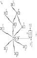
- FIG. 1 illustrates a wireless communications system 100 with access points 110 and user terminals 120, For simplicity, only one access point 110 is shown in FIG. 1 .
- An access point (AP) is generally a fixed station that communicates with the user terminals and may also be referred to as a base station (BS), an evolved Node B (eNB), or some other terminology.
- a user terminal (UT) may be fixed or mobile and may also be referred to as a mobile station (MS), an access terminal, user equipment (UE), a station (STA), a client, a wireless device, or some other terminology.
- a user terminal may be a wireless device, such as a cellular phone, a personal digital assistant (PDA), a handheld device, a wireless modem, a laptop computer, a tablet, a personal computer, etc.
- PDA personal digital assistant
- Access point 110 may communicate with one or more user terminals 120 at any given moment on the downlink and uplink.
- the downlink i.e., forward link
- the uplink i.e., reverse link
- a user terminal may also communicate peer-to-peer with another user terminal.
- a system controller 130 couples to and provides coordination and control for the access points.
- System 100 employs multiple transmit and multiple receive antennas for data transmission on the downlink and uplink.
- Access point 110 may be equipped with a number N ap of antennas to achieve transmit diversity for downlink transmissions and/or receive diversity for uplink transmissions.
- a set N u of selected user terminals 120 may receive downlink transmissions and transmit uplink transmissions.
- Each selected user terminal transmits user-specific data to and/or receives user-specific data from the access point.
- each selected user terminal may be equipped with one or multiple antennas (i.e., N ut ⁇ 1).
- the N u selected user terminals can have the same or different number of antennas,
- Wireless system 100 may be a time division duplex (TDD) system or a frequency division duplex (FDD) system.
- TDD time division duplex
- FDD frequency division duplex
- the downlink and uplink share the same frequency band
- the downlink and uplink use different frequency bands.
- System 100 may also utilize a single carrier or multiple carriers for transmission,
- Each user terminal may be equipped with a single antenna (e.g., in order to keep costs down) or multiple antennas (e.g., where the additional cost can be supported).
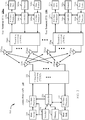
- FIG. 2 shows a block diagram of access point 110 and two user terminals 120m and 120x in wireless system 100.
- Access point 110 is equipped with N ap antennas 224a through 224ap.
- User terminal 120m is equipped with N ut,m antennas 252ma through 252mu
- user terminal 120x is equipped with N ut,x antennas 252xa through 252xu.
- Access point 110 is a transmitting entity for the downlink and a receiving entity for the uplink.
- Each user terminal 120 is a transmitting entity for the uplink and a receiving entity for the downlink.
- a “transmitting entity” is an independently operated apparatus or device capable of transmitting data via a frequency channel
- a “receiving entity” is an independently operated apparatus or device capable of receiving data via a frequency channel.
- the subscript " dn " denotes the downlink
- the subscript " up " denotes the uplink
- N up user terminals are selected for simultaneous transmission on the uplink
- N dn user terminals are selected for simultaneous transmission on the downlink
- N up may or may not be equal to N dn
- N up and N dn may be static values or can change for each scheduling interval. Beam-steering or some other spatial processing technique may be used at the access point and user terminal.
- a TX data processor 288 receives traffic data from a data source 286 and control data from a controller 280.
- TX data processor 288 processes (e.g., encodes, interleaves, and modulates) the traffic data ⁇ d up ⁇ for the user terminal based on the coding and modulation schemes associated with the rate selected for the user terminal and provides a data symbol stream ⁇ s up ⁇ for one of the N ut,m antennas.
- a transceiver front end (TX/RX) 254 receives and processes (e.g., converts to analog, amplifies, filters, and frequency upconverts) a respective symbol stream to generate an uplink signal.
- the transceiver front end 254 may also route the uplink signal to one of the N ut , m antennas for transmit diversity via an RF switch, for example.
- the controller 280 may control the routing within the transceiver front end 254.
- Memory 282 may store data and program codes for the user terminal 120 and may interface with the controller 280.
- a number N up of user terminals may be scheduled for simultaneous transmission on the uplink.
- Each of these user terminals transmits its set of processed symbol streams on the uplink to the access point.
- N ap antennas 224a through 224ap receive the uplink signals from all N up user terminals transmitting on the uplink.
- a transceiver front end 222 may select signals received from one of the antennas 224 for processing.
- a combination of the signals received from multiple antennas 224 may be combined for enhanced receive diversity.
- the access point's transceiver front end 222 also performs processing complementary to that performed by the user terminal's transceiver front end 254 and provides a recovered uplink data symbol stream.
- the recovered uplink data symbol stream is an estimate of a data symbol stream ⁇ s up ⁇ transmitted by a user terminal.
- An RX data processor 242 processes (e.g., demodulates, deinterleaves, and decodes) the recovered uplink data symbol stream in accordance with the rate used for that stream to obtain decoded data.
- the decoded data for each user terminal may be provided to a data sink 244 for storage and/or a controller 230 for further processing.
- a TX data processor 210 receives traffic data from a data source 208 for N dn user terminals scheduled for downlink transmission, control data from a controller 230 and possibly other data from a scheduler 234. The various types of data may be sent on different transport channels. TX data processor 210 processes (e.g., encodes, interleaves, and modulates) the traffic data for each user terminal based on the rate selected for that user terminal. TX data processor 210 may provide a downlink data symbol streams for one of more of the N dn user terminals to be transmitted from one of the N ap antennas.
- the transceiver front end 222 receives and processes (e.g., converts to analog, amplifies, filters, and frequency upconverts) the symbol stream to generate a downlink signal.
- the transceiver front end 222 may also route the downlink signal to one or more of the N ap antennas 224 for transmit diversity via an RF switch, for example.
- the controller 230 may control the routing within the transceiver front end 222.
- Memory 232 may store data and program codes for the access point 110 and may interface with the controller 230.
- N ut,m antennas 252 receive the downlink signals from access point 110.
- the transceiver front end 254 may select signals received from one of the antennas 252 for processing.
- a combination of the signals received from multiple antennas 252 may be combined for enhanced receive diversity.
- the user terminal's transceiver front end 254 also performs processing complementary to that performed by the access point's transceiver front end 222 and provides a recovered downlink data symbol stream.
- An RX data processor 270 processes (e.g., demodulates, deinterleaves, and decodes) the recovered downlink data symbol stream to obtain decoded data for the user terminal.
- TDMA Time Division Multiple Access
- SDMA Serial Advanced Code Division Multiple Access
- OFDMA Orthogonal Frequency Division Multiple Access
- CDMA Code Division Multiple Access
- SC-FDMA SC-FDMA
- TD-SCDMA Time Division Multiple Access
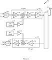
- FIG. 3 is a block diagram of an example transceiver front end 300, such as transceiver front ends 222, 254 in FIG. 2 , in accordance with certain aspects of the present disclosure.
- the transceiver front end 300 includes a transmit (TX) path 302 (also known as a transmit chain) for transmitting signals via one or more antennas and a receive (RX) path 304 (also known as a receive chain) for receiving signals via the antennas. If the TX path 302 and the RX path 304 share an antenna 303, the paths may be connected with the antenna via an interface 306, which may include any of various suitable RF devices, such as a duplexer, a switch, a diplexer, and the like.
- the TX path 302 may include a baseband filter (BBF) 310, a mixer 312, a driver amplifier (DA) 314, and a power amplifier 316.
- the BBF 310, the mixer 312, and the DA 314 may be included in a radio frequency integrated circuit (RFIC), while the PA 316 is often external to the RFIC.
- the BBF 310 filters the baseband signals received from the DAC 308, and the mixer 312 mixes the filtered baseband signals with a transmit local oscillator (LO) signal to convert the baseband signal of interest to a different frequency (e.g., upconvert from baseband to RF).
- LO transmit local oscillator
- This frequency conversion process produces the sum and difference frequencies of the LO frequency and the frequency of the signal of interest.
- the sum and difference frequencies are referred to as the beat frequencies.
- the beat frequencies are typically in the RF range, such that the signals output by the mixer 312 are typically RF signals, which are amplified by the DA 314 and by the PA 316 before transmission by the antenna 303.
- the RX path 304 includes a low noise amplifier (LNA) 322, a mixer 324, and a baseband filter (BBF) 326.
- the LNA 322, the mixer 324, and the BBF 326 may be included in a radio frequency integrated circuit (RFIC), which may or may not be the same RFIC that includes the TX path components.
- RFIC radio frequency integrated circuit
- RF signals received via the antenna 303 may be amplified by the LNA 322, and the mixer 324 mixes the amplified RF signals with a receive local oscillator (LO) signal to convert the RF signal of interest to a different baseband frequency (i.e., downconvert).
- the baseband signals output by the mixer 324 may be filtered by the BBF 326 before being converted by an analog-to-digital converter (ADC) 328 to digital I or Q signals for digital signal processing.
- ADC analog-to-digital converter
- the transmit LO is typically produced by a TX frequency synthesizer 318, which may be buffered or amplified by amplifier 320 before being mixed with the baseband signals in the mixer 312.
- the receive LO is typically produced by an RX frequency synthesizer 330, which may be buffered or amplified by amplifier 332 before being mixed with the RF signals in the mixer 324.
- diversity may be used to increase the reliability of transmissions by using two or more channels with different characteristics. Because individual channels experience different levels of fading and interference, multiple versions of the same signal may be received via different propagation paths in reception diversity in an effort to combat fading and interference.
- a 2-way diversity (a.k.a. ordinary diversity, as opposed to multi-way diversity) receiver may use two antennas associated with two different receive paths, one referred to as the "primary path” and the other referred to as the "diversity path.”
- RFFEs radio frequency front ends
- 4-way diversity receiver (4-RxD) is often desired.
- a conventional 2-way diversity receiver may be realized by sharing the local oscillator (LO) path between the primary receive path and the diversity receive path.
- a 4-way diversity receiver may be configured by driving 4 receive paths (e.g., RX path 304) with a single set consisting of a frequency synthesizer and corresponding LO path (which may include an amplifier or buffer and/or a divider).
- RX path 304 4 receive paths
- a single set consisting of a frequency synthesizer and corresponding LO path (which may include an amplifier or buffer and/or a divider).
- the performance and current consumption are usually poor.
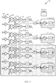
- FIG. 4 illustrates an example 4-way diversity receiver 400, in accordance with certain aspects of the present disclosure.
- the receiver 400 one set of frequency synthesizer 402 and corresponding LO path 404 is used to drive 4 or more receive paths.
- each receive path may include a low noise amplifier (LNA) 406, a balun 408 for single-ended to differential conversion, a mixer 410, a baseband filter (BBF) 412, and an analog-to-digital converter (ADC) 414 as illustrated in FIG. 4 .
- LNA low noise amplifier
- BBF baseband filter
- ADC analog-to-digital converter
- each receive path may include a differential LNA, a mixer, a BBF, and an ADC (i.e., without a balun for conversion).
- Each receive path may be associated with its own antenna 405.
- the frequency synthesizer 402 may include a voltage-controlled oscillator (VCO) 416 and a phase-locked loop (PLL) 418 and be followed by an amplifier 420 configured to amplify, buffer or attenuate the oscillating signal from the VCO 416.
- the frequency of the oscillating signal output by the amplifier 420 may be divided by a programmable frequency divider 422 to produce the LO signal with the local oscillating frequency ( f LO ) on the LO path 404,
- the LO path 404 may have both in-phase (I) and quadrature (Q) components.
- the current consumption of the LO path 404 is usually high due to the mixer loading. Furthermore, the phase noise performance is poor due to the limited swing. It is challenging to comply with such design specifications as the far-out phase noise at the duplex frequency and the large-signal noise figure, Current consumption may be further increased to meet the phase noise and noise figure specifications.
- Certain aspects of the present disclosure provide multi-way diversity receivers, where at most two receive paths in the diversity receiver share a frequency synthesizer and corresponding LO path.
- Such a multi-way diversity receiver may be implemented in a carrier aggregation (CA) transceiver.
- CA carrier aggregation
- Carrier aggregation is used in some radio access technologies (RATs), such as LTE-A, in an effort to increase the bandwidth, and thereby increase bitrates.
- RATs radio access technologies
- multiple frequency resources i.e., carriers
- CC component carrier
- LTE Rel-10 for example, up to five component carriers can be aggregated, leading to a maximum aggregated bandwidth of 100 MHz.
- the allocation of resources may be contiguous or non-contiguous. Non-contiguous allocation may be either intra-band (i.e., the component carriers belong to the same operating frequency band, but have one or more gaps in between) or inter-band, in which case the component carriers belong to different operating frequency bands.
- RFFEs radio frequency front ends
- various CA transceivers have been developed.
- a 4-way diversity receiver (4 RxD) may be configured by using 2 sets of synthesizers plus corresponding LO paths, generating the same LO frequency, to drive 4 receive paths.
- FIG. 5 illustrates an example 4-way diversity receiver 500 implemented in a 4-CA transceiver where the 4 receive paths of interest are driven by 2 frequency synthesizing circuits (synthesizers 402 0 , 402 1 ), in accordance with certain aspects of the present disclosure.
- the first LO frequency ( f LO0 ) generated by the first frequency synthesizing circuit (labeled “CA0 Synth") is the same as the second LO frequency ( f LO1 ) generated by the second frequency synthesizing circuit (labeled "CA1 Synth").
- the 4-way diversity receiver 500 has increased performance compared to the 4-way diversity receiver 400 of FIG. 4 .
- the LO signal swing and phase noise is better in the receiver 500 because LO loading is distributed between the 2 frequency synthesizers 402 0 , 402 1 .
- a portion (e.g., half) of the 4-CA transceiver may be disabled as shown for certain aspects.
- the first four receive paths and first two CA synthesizing circuits (CA0 and CA1) are enabled in the receiver 500 of FIG. 5
- any suitable CA synthesizing circuits and receive paths may be enabled instead of those shown.
- a 3-way diversity receiver may be configured instead by enabling 2 sets of synthesizers (e.g., synthesizers 402 0 , 402 1 ) plus corresponding LO paths 404 0 , 404 1 , generating the same LO frequency, to drive 3 receive paths 602, 604, 606.
- FIG. 6 illustrates an example 3-way diversity receiver 600 implemented in the CA transceiver of FIG. 5 , in accordance with certain aspects of the present disclosure.
- any two suitable CA synthesizing circuits and three receive paths may be enabled instead of those shown to implement a 3-RxD.
- the diversity path 608 associated with CA1 Synth may be disabled as depicted in FIG. 6
- the primary path 606 associated with CA1 Synth may be disabled instead.
- the primary path 602 or the diversity path 604, both associated with CA0 Synth may be disabled instead of the diversity path 608 associated with CA1 Synth.
- a 2-carrier, 4-way diversity receiver may be configured by enabling 4 sets of synthesizers plus corresponding LO paths, generating 2 different LO frequencies, to drive 8 receive paths.
- FIG. 7A illustrates an example 2-carrier, 4-way diversity receiver 700 implemented in the CA transceiver of FIG. 5 , in accordance with certain aspects of the present disclosure.
- the first LO frequency ( f L O0 ) generated by the first frequency synthesizing circuit (CA0 Synth) is the same as the second LO frequency ( f L O1 ) generated by the second frequency synthesizing circuit (CA1 Synth).
- the third LO frequency ( f L O2 ) generated by the third frequency synthesizing circuit (CA2 Synth) is the same as the fourth LO frequency ( f L O3 ) generated by the fourth frequency synthesizing circuit (CA3 Synth),
- the first four receive paths 602, 604, 606, 608 may be designated for a first carrier as shown, whereas the second four receive paths 702, 704, 706, 708 may be designated for a second carrier, different from the first carrier.
- first four receive paths 602, 604, 606, 608 and first two CA synthesizing circuits (CA0 Synth and CA1 Synth) are used for the first carrier in the receiver 700 of FIG, 7A
- any suitable CA synthesizing circuits and receive paths may be designated for the first carrier.
- the 8 receive paths in the CA transceiver may be used in a similar configuration to implement an 8-way diversity receiver (8 RxD) (all with the same LO frequency), rather than a 2-carrier, 4 RxD.
- the 2-carrier, 4-way diversity receiver 700 has increased performance compared to the 4-way diversity receiver 400 of FIG. 4 .
- the improvement in the phase noise and noise figure is even more significant because the LO loading is distributed among four frequency synthesizers 402 0-3 .
- the overall reduction in the current consumption is significant.
- a 2-carrier, 3-way diversity receiver may be configured by enabling 4 sets of synthesizers plus corresponding LO paths, generating 2 different LO frequencies, to drive 6 receive paths
- FIG. 7B illustrates an example 2-carrier, 3-way diversity receiver 750 implemented in the CA transceiver of FIG.
- the first LO frequency ( f LO0 ) generated by the first frequency synthesizing circuit (CA0 Synth) is the same as the second LO frequency ( f LO1 ) generated by the second frequency synthesizing circuit (CA1 Synth),
- the third LO frequency ( f L O2 ) generated by the third frequency synthesizing circuit (CA2 Synth) is the same as the fourth LO frequency ( f L O3 ) generated by the fourth frequency synthesizing circuit (CA3 Synth).
- three receive paths 602, 604, 606 may be designated for a first carrier as shown, whereas three other receive paths 702, 704, 706 may be designated for a second carrier, different from the first carrier.
- the 6 receive paths in the CA transceiver may be used in a similar configuration to implement a 6-way diversity receiver (6 RxD) (all with the same LO frequency), rather than a 2-carrier, 3 RxD.
- first three receive paths 602, 604, 606 and first two CA synthesizing circuits (CA0 Synth and CA1 Synth) are used for the first carrier in the receiver 750 of FIG. 7B
- any suitable CA synthesizing circuits and receive paths may be designated for the first carrier.
- three receive paths 606, 608, 702 may be designated for the first carrier, whereas three other receive paths 604, 706, 708 may be designated for the second carrier.
- the second LO frequency ( f LO1 ) generated by the second frequency synthesizing circuit (CA1 Synth) is the same as the third LO frequency ( f LO2 ) generated by the third frequency synthesizing circuit (CA2 Synth), whereas the first LO frequency ( f LO0 ) generated by the first frequency synthesizing circuit (CA0 Synth) is the same as the fourth LO frequency ( f LO3 ) generated by the fourth frequency synthesizing circuit (CA3 Synth).
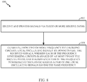
- FIG. 8 is a flow diagram of example operations 800 for using multi-way diversity receivers with multiple frequency synthesizing circuits.
- the operations 800 may be performed, for example, by a multi-way diversity receiver or a CA transceiver described above, such as the 4-way diversity receiver 400.
- the operations 800 may begin, at block 802, with the diversity receiver receiving and processing signals via three or more receive paths.
- the diversity receiver may generate, from two or more frequency synthesizing circuits, local oscillating signals to downconvert the received signals.
- Each of the frequency synthesizing circuits may be shared by at most two of the receive paths.
- Each pair of the frequency synthesizing circuits may generate a pair of the local oscillating signals having the same frequency.
- the three or more receive paths include 8 receive paths, and the two or more frequency synthesizing circuits include 4 frequency synthesizing circuits.
- the generating at block 804 may involve generating a first two local oscillating signals having the same first frequency with a first pair of the 4 frequency synthesizing circuits.
- the generating at block 804 may also entail generating a second two local oscillating signals having the same second frequency with a second pair of the 4 frequency synthesizing circuits,
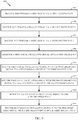
- FIG. 9 is a flow diagram of example operations 900 for employing multi-way diversity receivers with multiple frequency synthesizing circuits.
- the operations 900 may be performed, for example, by a multi-way diversity receiver or a CA transceiver described above, such as the 4-way diversity receiver 400.
- the operations 900 may begin, at block 902, with the diversity receiver receiving and processing a first signal via a first receive path.
- the diversity receiver may receive and process a second signal via a second receive path and receive and process a third signal via a third receive path, respectively.
- the diversity receiver may generate a first local oscillating signal having a first frequency at block 908.
- the diversity receiver may mix the first local oscillating signal with the processed first signal via a first mixing circuit in the first receive path and mix the first local oscillating signal with the processed second signal via a second mixing circuit in the second receive path, respectively.
- the diversity receiver may generate a second local oscillating signal having a second frequency equal to the first frequency at block 914.
- the diversity receiver may mix the second local oscillating signal with the processed third signal via a third mixing circuit in the third receive path.
- the operations 900 may further involve the diversity receiver receiving and processing a fourth signal via a fourth receive path.
- the diversity receiver may mix the second local oscillating signal with the processed fourth signal via a fourth mixing circuit in the fourth receive path.
- the operations 900 may further entail the diversity receiver receiving and processing a fifth signal via a fifth receive path and receiving and processing a sixth signal via a sixth receive path.
- the diversity receiver may generate a third local oscillating signal having a third frequency, mix the third local oscillating signal with the processed fifth signal via a fifth mixing circuit in the fifth receive path, and mix the third local oscillating signal with the processed sixth signal via a sixth mixing circuit in the sixth receive path.
- the operations 900 may further include the diversity receiver receiving and processing a seventh signal via a seventh receive path and receiving and processing an eighth signal via an eighth receive path.
- the diversity receiver may generate a fourth local oscillating signal having a fourth frequency, mix the fourth local oscillating signal with the processed seventh signal via a seventh mixing circuit in the seventh receive path, and mix the fourth local oscillating signal with the processed eighth signal via an eighth mixing circuit in the eighth receive path.
- the various operations or methods described above may be performed by any suitable means capable of performing the corresponding functions.
- the means may include various hardware and/or software component(s) and/or module(s), including, but not limited to a circuit, an application specific integrated circuit (ASIC), or processor.
- ASIC application specific integrated circuit
- means for transmitting may comprise a transmitter (e.g., the transceiver front end 254 of the user terminal 120 depicted in FIG. 2 or the transceiver front end 222 of the access point 110 shown in FIG. 2 ) and/or an antenna (e.g., the antennas 252ma through 252mu of the user terminal 120m portrayed in FIG. 2 or the antennas 224a through 224ap of the access point 110 illustrated in FIG. 2 ).
- Means for receiving may comprise a receiver (e.g., the transceiver front end 254 of the user terminal 120 depicted in FIG. 2 or the transceiver front end 222 of the access point 110 shown in FIG.
- Means for processing or means for determining may comprise a processing system, which may include one or more processors, such as the RX data processor 270, the TX data processor 288, and/or the controller 280 of the user terminal 120 illustrated in FIG. 2 .
- determining encompasses a wide variety of actions. For example, “determining” may include calculating, computing, processing, deriving, investigating, looking up (e.g., looking up in a table, a database or another data structure), ascertaining and the like. Also, “determining” may include receiving (e.g., receiving information), accessing (e.g., accessing data in a memory) and the like. Also, “determining” may include resolving, selecting, choosing, establishing and the like.
- a phrase referring to "at least one of" a list of items refers to any combination of those items, including single members.
- "at least one of: a, b, or c" is intended to cover: a, b, c, a-b, a-c, b-c, a-b-c, as well as any combination with multiples of the same element (e.g., a-a, a-a-a , a-a-b, a-a-c, a-b-b, a-c-c, b-b, b-b-b, b-b-c, c-c, and c-c-c or any other ordering of a, b, and c ).
- DSP digital signal processor
- ASIC application specific integrated circuit
- FPGA field programmable gate array
- PLD programmable logic device
- a general-purpose processor may be a microprocessor, but in the alternative, the processor may be any commercially available processor, controller, microcontroller, or state machine.
- a processor may also be implemented as a combination of computing devices, e.g., a combination of a DSP and a microprocessor, a plurality of microprocessors, one or more microprocessors in conjunction with a DSP core, or any other such configuration.
- the methods disclosed herein comprise one or more steps or actions for achieving the described method.
- the method steps and/or actions may be interchanged with one another without departing from the scope of the claims.
- the order and/or use of specific steps and/or actions may be modified without departing from the scope of the claims.
- an example hardware configuration may comprise a processing system in a wireless node.
- the processing system may be implemented with a bus architecture.
- the bus may include any number of interconnecting buses and bridges depending on the specific application of the processing system and the overall design constraints.
- the bus may link together various circuits including a processor, machine-readable media, and a bus interface.
- the bus interface may be used to connect a network adapter, among other things, to the processing system via the bus.
- the network adapter may be used to implement the signal processing functions of the PHY layer.
- a user terminal 120 see FIG.
- a user interface e.g., keypad, display, mouse, joystick, etc.
- the bus may also link various other circuits such as timing sources, peripherals, voltage regulators, power management circuits, and the like, which are well known in the art, and therefore, will not be described any further.
- the processing system may be configured as a general-purpose processing system with one or more microprocessors providing the processor functionality and external memory providing at least a portion of the machine-readable media, all linked together with other supporting circuitry through an external bus architecture.
- the processing system may be implemented with an ASIC (Application Specific Integrated Circuit) with the processor, the bus interface, the user interface in the case of an access terminal), supporting circuitry, and at least a portion of the machine-readable media integrated into a single chip, or with one or more FPGAs (Field Programmable Gate Arrays), PLDs (Programmable Logic Devices), controllers, state machines, gated logic, discrete hardware components, or any other suitable circuitry, or any combination of circuits that can perform the various functionality described throughout this disclosure.
- FPGAs Field Programmable Gate Arrays
- PLDs Programmable Logic Devices
- controllers state machines, gated logic, discrete hardware components, or any other suitable circuitry, or any combination of circuits that can perform the various functionality described throughout this disclosure.
Landscapes
- Engineering & Computer Science (AREA)
- Computer Networks & Wireless Communication (AREA)
- Signal Processing (AREA)
- Physics & Mathematics (AREA)
- Spectroscopy & Molecular Physics (AREA)
- Radio Transmission System (AREA)
Applications Claiming Priority (3)
| Application Number | Priority Date | Filing Date | Title |
|---|---|---|---|
| US201461993325P | 2014-05-15 | 2014-05-15 | |
| US14/677,056 US9712226B2 (en) | 2014-05-15 | 2015-04-02 | Multi-way diversity receiver with multiple synthesizers in a carrier aggregation transceiver |
| PCT/US2015/024189 WO2015175109A1 (en) | 2014-05-15 | 2015-04-03 | Multi-way diversity receiver with multiple synthesizers in a carrier aggregation transceiver |
Publications (2)
| Publication Number | Publication Date |
|---|---|
| EP3143699A1 EP3143699A1 (en) | 2017-03-22 |
| EP3143699B1 true EP3143699B1 (en) | 2019-07-17 |
Family
ID=53053077
Family Applications (1)
| Application Number | Title | Priority Date | Filing Date |
|---|---|---|---|
| EP15720823.2A Active EP3143699B1 (en) | 2014-05-15 | 2015-04-03 | Multi-way diversity receiver with multiple synthesizers in a carrier aggregation transceiver |
Country Status (6)
| Country | Link |
|---|---|
| US (2) | US9712226B2 (enExample) |
| EP (1) | EP3143699B1 (enExample) |
| JP (1) | JP6585083B2 (enExample) |
| KR (1) | KR102304289B1 (enExample) |
| CN (1) | CN106464276B (enExample) |
| WO (1) | WO2015175109A1 (enExample) |
Families Citing this family (17)
| Publication number | Priority date | Publication date | Assignee | Title |
|---|---|---|---|---|
| US9712226B2 (en) | 2014-05-15 | 2017-07-18 | Qualcomm Incorporated | Multi-way diversity receiver with multiple synthesizers in a carrier aggregation transceiver |
| US9525503B2 (en) * | 2014-05-28 | 2016-12-20 | Qualcomm Incorporated | Reconfigurable multi-mode transceiver |
| DK3355478T3 (da) * | 2014-09-10 | 2019-11-04 | Ericsson Telefon Ab L M | Radiomodtager til bæreraggregering |
| US20170170998A1 (en) * | 2015-12-11 | 2017-06-15 | Nokia Solutions And Networks Oy | Pre-combiner interference removal |
| KR102557997B1 (ko) * | 2017-12-05 | 2023-07-21 | 삼성전자주식회사 | 반송파 집적(Carrier Aggregation)을 이용하여 신호를 송수신하는 RFIC 및 이를 포함하는 무선 통신 장치 |
| US10560128B2 (en) | 2017-12-05 | 2020-02-11 | Samsung Electronics Co., Ltd. | Carrier aggregated signal transmission and reception |
| KR101940691B1 (ko) | 2018-02-01 | 2019-01-22 | 주식회사 우드메탈 | 내진성능을 가지는 가구용 받침장치 |
| KR102427572B1 (ko) * | 2018-06-18 | 2022-08-01 | 삼성전자주식회사 | 스위치를 통해 복수개의 반송파 주파수를 이용한 반송파 집적을 수행하는 전자 장치 및 그의 동작 방법 |
| KR102000073B1 (ko) | 2018-12-26 | 2019-07-16 | 주식회사 우드메탈 | 가구용 높낮이조절 받침장치 |
| US10720953B1 (en) | 2019-05-30 | 2020-07-21 | Shure Acquisition Holdings, Inc. | Scalable diversity deployment for wide tuning range transceiver |
| KR102653890B1 (ko) * | 2019-10-18 | 2024-04-02 | 삼성전자주식회사 | 반송파 집성을 지원하는 rfic 및 이를 포함하는 무선 통신 장치 |
| KR102653889B1 (ko) * | 2019-10-18 | 2024-04-02 | 삼성전자주식회사 | 반송파 집성을 지원하는 수신기 및 이를 포함하는 무선 통신 장치 |
| KR102197809B1 (ko) | 2019-11-28 | 2021-01-04 | 주식회사 우드메탈 | 내진과 외부 충격 시에 좌우 진동을 흡수하는 수납 가구용 조절장치 |
| CN111313928B (zh) * | 2020-02-13 | 2021-12-28 | 广州全盛威信息技术有限公司 | 支持多种制式的超宽带收发机架构及相应的无线门禁装置 |
| US11695535B2 (en) * | 2021-03-11 | 2023-07-04 | Xilinx, Inc. | Reconfigurable mixer design enabling multiple radio architectures |
| KR102439161B1 (ko) | 2022-04-04 | 2022-09-01 | 주식회사 우드메탈 | 가구 내부에서 손쉽게 높이를 조절할 수 있는 조절발을 구비한 수납가구 |
| CN115412106A (zh) * | 2022-07-12 | 2022-11-29 | 北京中科睿谱科技有限公司 | 一种多通道高隔离度差分开关矩阵电路 |
Family Cites Families (19)
| Publication number | Priority date | Publication date | Assignee | Title |
|---|---|---|---|---|
| JP2003179530A (ja) * | 2001-12-10 | 2003-06-27 | Alps Electric Co Ltd | 受信装置 |
| KR100550318B1 (ko) * | 2003-10-30 | 2006-02-07 | 주식회사 팬택앤큐리텔 | 자기위치정보와 디지털 멀티미디어 방송(dmb)수신기능을 갖는 무선통신 단말기용 rf 수신기 |
| JP4327666B2 (ja) * | 2004-06-23 | 2009-09-09 | 株式会社ルネサステクノロジ | 無線送信回路及びそれを用いた送受信機 |
| US8254865B2 (en) * | 2006-04-07 | 2012-08-28 | Belair Networks | System and method for frequency offsetting of information communicated in MIMO-based wireless networks |
| US20080287163A1 (en) | 2007-05-17 | 2008-11-20 | Telefonaktiebolaget Lm Ericsson (Publ), | Method and apparatus for converting between a multi-sector, omni-base station configuration and a multi-sector base station configuration |
| JP2009044446A (ja) * | 2007-08-08 | 2009-02-26 | Sanyo Electric Co Ltd | 受信装置 |
| US8055211B2 (en) | 2007-12-31 | 2011-11-08 | Motorola Mobility, Inc. | Method and system for utilizing transmit local oscillator for improved cell search and multi-link communication in multi-mode device |
| JP2010273283A (ja) * | 2009-05-25 | 2010-12-02 | Mitsubishi Electric Corp | 送受信装置 |
| WO2011094284A1 (en) * | 2010-01-26 | 2011-08-04 | Maxlinear, Inc. | Diversity receiver |
| US8892057B2 (en) | 2011-08-23 | 2014-11-18 | Rf Micro Devices, Inc. | Carrier aggregation radio system |
| US8756451B2 (en) * | 2011-10-01 | 2014-06-17 | Intel Corporation | Frequency synthesis methods and systems |
| JP5375925B2 (ja) * | 2011-11-01 | 2013-12-25 | 株式会社デンソー | 無線通信機 |
| US9143085B2 (en) | 2012-03-01 | 2015-09-22 | Qualcomm Incorporated | Frequency synthesizer architecture in a time-division duplex mode for a wireless device |
| US9172402B2 (en) | 2012-03-02 | 2015-10-27 | Qualcomm Incorporated | Multiple-input and multiple-output carrier aggregation receiver reuse architecture |
| US9118439B2 (en) * | 2012-04-06 | 2015-08-25 | Qualcomm Incorporated | Receiver for imbalanced carriers |
| US9185705B2 (en) * | 2012-06-19 | 2015-11-10 | Samsung Electronics Co., Ltd. | Apparatus and methods for flexible RF configuration in multi-antenna wireless systems |
| US9014648B2 (en) | 2012-12-21 | 2015-04-21 | Qualcomm Incorporated | Diversity receiver with shared local oscillator signal in diversity mode |
| KR101351589B1 (ko) * | 2013-01-30 | 2014-01-16 | 한국과학기술원 | 다중 안테나 송수신 시스템 |
| US9712226B2 (en) | 2014-05-15 | 2017-07-18 | Qualcomm Incorporated | Multi-way diversity receiver with multiple synthesizers in a carrier aggregation transceiver |
-
2015
- 2015-04-02 US US14/677,056 patent/US9712226B2/en active Active
- 2015-04-03 CN CN201580025166.1A patent/CN106464276B/zh active Active
- 2015-04-03 KR KR1020167031213A patent/KR102304289B1/ko active Active
- 2015-04-03 EP EP15720823.2A patent/EP3143699B1/en active Active
- 2015-04-03 JP JP2016567505A patent/JP6585083B2/ja active Active
- 2015-04-03 WO PCT/US2015/024189 patent/WO2015175109A1/en not_active Ceased
-
2017
- 2017-06-29 US US15/638,215 patent/US10250314B2/en active Active
Non-Patent Citations (1)
| Title |
|---|
| None * |
Also Published As
| Publication number | Publication date |
|---|---|
| JP2017521889A (ja) | 2017-08-03 |
| US20150333815A1 (en) | 2015-11-19 |
| US9712226B2 (en) | 2017-07-18 |
| JP6585083B2 (ja) | 2019-10-02 |
| WO2015175109A1 (en) | 2015-11-19 |
| US10250314B2 (en) | 2019-04-02 |
| US20170302358A1 (en) | 2017-10-19 |
| EP3143699A1 (en) | 2017-03-22 |
| KR102304289B1 (ko) | 2021-09-17 |
| CN106464276B (zh) | 2019-05-28 |
| CN106464276A (zh) | 2017-02-22 |
| KR20170007283A (ko) | 2017-01-18 |
Similar Documents
| Publication | Publication Date | Title |
|---|---|---|
| EP3143699B1 (en) | Multi-way diversity receiver with multiple synthesizers in a carrier aggregation transceiver | |
| CN107113033B (zh) | 用于在载波聚合(ca)模式的接收机受限的用户设备中动态地配置一个或多个小区的方法和装置 | |
| US9356769B2 (en) | Synchronous reset and phase detecting for interchain local oscillator (LO) divider phase alignment | |
| EP3100358B1 (en) | Differential bang-bang phase detector using standard digital cells | |
| US9681447B2 (en) | Dynamic local oscillator (LO) scheme and switchable receive (RX) chain for carrier aggregation | |
| US9356768B2 (en) | Phase detecting circuit for interchain local oscillator (LO) divider phase alignment | |
| US20150092683A1 (en) | Dynamic secondary cell (scell) allocation and frequency planning for carrier aggregation | |
| CN107925411A (zh) | 用于使用脉冲吞没技术使分频器同步的方法和装置 | |
| US9685931B2 (en) | High accuracy millimeter wave/radio frequency wideband in-phase and quadrature generation | |
| US20150078497A1 (en) | Receiver carrier aggregation frequency generation | |
| EP3613149B1 (en) | Mechanism to mitigate transmitter and receiver voltage-controlled oscillator (vco) pulling | |
| US20160079985A1 (en) | Quadrature local oscillator phase synthesis and architecture for divide-by-odd-number frequency dividers |
Legal Events
| Date | Code | Title | Description |
|---|---|---|---|
| STAA | Information on the status of an ep patent application or granted ep patent |
Free format text: STATUS: THE INTERNATIONAL PUBLICATION HAS BEEN MADE |
|
| PUAI | Public reference made under article 153(3) epc to a published international application that has entered the european phase |
Free format text: ORIGINAL CODE: 0009012 |
|
| STAA | Information on the status of an ep patent application or granted ep patent |
Free format text: STATUS: REQUEST FOR EXAMINATION WAS MADE |
|
| 17P | Request for examination filed |
Effective date: 20161006 |
|
| AK | Designated contracting states |
Kind code of ref document: A1 Designated state(s): AL AT BE BG CH CY CZ DE DK EE ES FI FR GB GR HR HU IE IS IT LI LT LU LV MC MK MT NL NO PL PT RO RS SE SI SK SM TR |
|
| AX | Request for extension of the european patent |
Extension state: BA ME |
|
| DAV | Request for validation of the european patent (deleted) | ||
| DAX | Request for extension of the european patent (deleted) | ||
| STAA | Information on the status of an ep patent application or granted ep patent |
Free format text: STATUS: EXAMINATION IS IN PROGRESS |
|
| 17Q | First examination report despatched |
Effective date: 20180124 |
|
| GRAP | Despatch of communication of intention to grant a patent |
Free format text: ORIGINAL CODE: EPIDOSNIGR1 |
|
| STAA | Information on the status of an ep patent application or granted ep patent |
Free format text: STATUS: GRANT OF PATENT IS INTENDED |
|
| INTG | Intention to grant announced |
Effective date: 20190206 |
|
| GRAS | Grant fee paid |
Free format text: ORIGINAL CODE: EPIDOSNIGR3 |
|
| GRAA | (expected) grant |
Free format text: ORIGINAL CODE: 0009210 |
|
| STAA | Information on the status of an ep patent application or granted ep patent |
Free format text: STATUS: THE PATENT HAS BEEN GRANTED |
|
| AK | Designated contracting states |
Kind code of ref document: B1 Designated state(s): AL AT BE BG CH CY CZ DE DK EE ES FI FR GB GR HR HU IE IS IT LI LT LU LV MC MK MT NL NO PL PT RO RS SE SI SK SM TR |
|
| REG | Reference to a national code |
Ref country code: GB Ref legal event code: FG4D |
|
| REG | Reference to a national code |
Ref country code: CH Ref legal event code: EP |
|
| REG | Reference to a national code |
Ref country code: IE Ref legal event code: FG4D |
|
| REG | Reference to a national code |
Ref country code: DE Ref legal event code: R096 Ref document number: 602015033895 Country of ref document: DE |
|
| REG | Reference to a national code |
Ref country code: AT Ref legal event code: REF Ref document number: 1156763 Country of ref document: AT Kind code of ref document: T Effective date: 20190815 |
|
| REG | Reference to a national code |
Ref country code: NL Ref legal event code: MP Effective date: 20190717 |
|
| REG | Reference to a national code |
Ref country code: LT Ref legal event code: MG4D |
|
| REG | Reference to a national code |
Ref country code: AT Ref legal event code: MK05 Ref document number: 1156763 Country of ref document: AT Kind code of ref document: T Effective date: 20190717 |
|
| PG25 | Lapsed in a contracting state [announced via postgrant information from national office to epo] |
Ref country code: NO Free format text: LAPSE BECAUSE OF FAILURE TO SUBMIT A TRANSLATION OF THE DESCRIPTION OR TO PAY THE FEE WITHIN THE PRESCRIBED TIME-LIMIT Effective date: 20191017 Ref country code: BG Free format text: LAPSE BECAUSE OF FAILURE TO SUBMIT A TRANSLATION OF THE DESCRIPTION OR TO PAY THE FEE WITHIN THE PRESCRIBED TIME-LIMIT Effective date: 20191017 Ref country code: AT Free format text: LAPSE BECAUSE OF FAILURE TO SUBMIT A TRANSLATION OF THE DESCRIPTION OR TO PAY THE FEE WITHIN THE PRESCRIBED TIME-LIMIT Effective date: 20190717 Ref country code: HR Free format text: LAPSE BECAUSE OF FAILURE TO SUBMIT A TRANSLATION OF THE DESCRIPTION OR TO PAY THE FEE WITHIN THE PRESCRIBED TIME-LIMIT Effective date: 20190717 Ref country code: LT Free format text: LAPSE BECAUSE OF FAILURE TO SUBMIT A TRANSLATION OF THE DESCRIPTION OR TO PAY THE FEE WITHIN THE PRESCRIBED TIME-LIMIT Effective date: 20190717 Ref country code: NL Free format text: LAPSE BECAUSE OF FAILURE TO SUBMIT A TRANSLATION OF THE DESCRIPTION OR TO PAY THE FEE WITHIN THE PRESCRIBED TIME-LIMIT Effective date: 20190717 Ref country code: PT Free format text: LAPSE BECAUSE OF FAILURE TO SUBMIT A TRANSLATION OF THE DESCRIPTION OR TO PAY THE FEE WITHIN THE PRESCRIBED TIME-LIMIT Effective date: 20191118 Ref country code: FI Free format text: LAPSE BECAUSE OF FAILURE TO SUBMIT A TRANSLATION OF THE DESCRIPTION OR TO PAY THE FEE WITHIN THE PRESCRIBED TIME-LIMIT Effective date: 20190717 Ref country code: SE Free format text: LAPSE BECAUSE OF FAILURE TO SUBMIT A TRANSLATION OF THE DESCRIPTION OR TO PAY THE FEE WITHIN THE PRESCRIBED TIME-LIMIT Effective date: 20190717 |
|
| PG25 | Lapsed in a contracting state [announced via postgrant information from national office to epo] |
Ref country code: AL Free format text: LAPSE BECAUSE OF FAILURE TO SUBMIT A TRANSLATION OF THE DESCRIPTION OR TO PAY THE FEE WITHIN THE PRESCRIBED TIME-LIMIT Effective date: 20190717 Ref country code: GR Free format text: LAPSE BECAUSE OF FAILURE TO SUBMIT A TRANSLATION OF THE DESCRIPTION OR TO PAY THE FEE WITHIN THE PRESCRIBED TIME-LIMIT Effective date: 20191018 Ref country code: IS Free format text: LAPSE BECAUSE OF FAILURE TO SUBMIT A TRANSLATION OF THE DESCRIPTION OR TO PAY THE FEE WITHIN THE PRESCRIBED TIME-LIMIT Effective date: 20191117 Ref country code: RS Free format text: LAPSE BECAUSE OF FAILURE TO SUBMIT A TRANSLATION OF THE DESCRIPTION OR TO PAY THE FEE WITHIN THE PRESCRIBED TIME-LIMIT Effective date: 20190717 Ref country code: LV Free format text: LAPSE BECAUSE OF FAILURE TO SUBMIT A TRANSLATION OF THE DESCRIPTION OR TO PAY THE FEE WITHIN THE PRESCRIBED TIME-LIMIT Effective date: 20190717 Ref country code: ES Free format text: LAPSE BECAUSE OF FAILURE TO SUBMIT A TRANSLATION OF THE DESCRIPTION OR TO PAY THE FEE WITHIN THE PRESCRIBED TIME-LIMIT Effective date: 20190717 |
|
| PG25 | Lapsed in a contracting state [announced via postgrant information from national office to epo] |
Ref country code: TR Free format text: LAPSE BECAUSE OF FAILURE TO SUBMIT A TRANSLATION OF THE DESCRIPTION OR TO PAY THE FEE WITHIN THE PRESCRIBED TIME-LIMIT Effective date: 20190717 |
|
| PG25 | Lapsed in a contracting state [announced via postgrant information from national office to epo] |
Ref country code: IT Free format text: LAPSE BECAUSE OF FAILURE TO SUBMIT A TRANSLATION OF THE DESCRIPTION OR TO PAY THE FEE WITHIN THE PRESCRIBED TIME-LIMIT Effective date: 20190717 Ref country code: RO Free format text: LAPSE BECAUSE OF FAILURE TO SUBMIT A TRANSLATION OF THE DESCRIPTION OR TO PAY THE FEE WITHIN THE PRESCRIBED TIME-LIMIT Effective date: 20190717 Ref country code: DK Free format text: LAPSE BECAUSE OF FAILURE TO SUBMIT A TRANSLATION OF THE DESCRIPTION OR TO PAY THE FEE WITHIN THE PRESCRIBED TIME-LIMIT Effective date: 20190717 Ref country code: EE Free format text: LAPSE BECAUSE OF FAILURE TO SUBMIT A TRANSLATION OF THE DESCRIPTION OR TO PAY THE FEE WITHIN THE PRESCRIBED TIME-LIMIT Effective date: 20190717 Ref country code: PL Free format text: LAPSE BECAUSE OF FAILURE TO SUBMIT A TRANSLATION OF THE DESCRIPTION OR TO PAY THE FEE WITHIN THE PRESCRIBED TIME-LIMIT Effective date: 20190717 |
|
| PG25 | Lapsed in a contracting state [announced via postgrant information from national office to epo] |
Ref country code: CZ Free format text: LAPSE BECAUSE OF FAILURE TO SUBMIT A TRANSLATION OF THE DESCRIPTION OR TO PAY THE FEE WITHIN THE PRESCRIBED TIME-LIMIT Effective date: 20190717 Ref country code: SK Free format text: LAPSE BECAUSE OF FAILURE TO SUBMIT A TRANSLATION OF THE DESCRIPTION OR TO PAY THE FEE WITHIN THE PRESCRIBED TIME-LIMIT Effective date: 20190717 Ref country code: IS Free format text: LAPSE BECAUSE OF FAILURE TO SUBMIT A TRANSLATION OF THE DESCRIPTION OR TO PAY THE FEE WITHIN THE PRESCRIBED TIME-LIMIT Effective date: 20200224 Ref country code: SM Free format text: LAPSE BECAUSE OF FAILURE TO SUBMIT A TRANSLATION OF THE DESCRIPTION OR TO PAY THE FEE WITHIN THE PRESCRIBED TIME-LIMIT Effective date: 20190717 |
|
| REG | Reference to a national code |
Ref country code: DE Ref legal event code: R097 Ref document number: 602015033895 Country of ref document: DE |
|
| PLBE | No opposition filed within time limit |
Free format text: ORIGINAL CODE: 0009261 |
|
| STAA | Information on the status of an ep patent application or granted ep patent |
Free format text: STATUS: NO OPPOSITION FILED WITHIN TIME LIMIT |
|
| PG2D | Information on lapse in contracting state deleted |
Ref country code: IS |
|
| 26N | No opposition filed |
Effective date: 20200603 |
|
| PG25 | Lapsed in a contracting state [announced via postgrant information from national office to epo] |
Ref country code: SI Free format text: LAPSE BECAUSE OF FAILURE TO SUBMIT A TRANSLATION OF THE DESCRIPTION OR TO PAY THE FEE WITHIN THE PRESCRIBED TIME-LIMIT Effective date: 20190717 |
|
| PG25 | Lapsed in a contracting state [announced via postgrant information from national office to epo] |
Ref country code: MC Free format text: LAPSE BECAUSE OF FAILURE TO SUBMIT A TRANSLATION OF THE DESCRIPTION OR TO PAY THE FEE WITHIN THE PRESCRIBED TIME-LIMIT Effective date: 20190717 |
|
| REG | Reference to a national code |
Ref country code: CH Ref legal event code: PL |
|
| PG25 | Lapsed in a contracting state [announced via postgrant information from national office to epo] |
Ref country code: CH Free format text: LAPSE BECAUSE OF NON-PAYMENT OF DUE FEES Effective date: 20200430 Ref country code: LU Free format text: LAPSE BECAUSE OF NON-PAYMENT OF DUE FEES Effective date: 20200403 Ref country code: LI Free format text: LAPSE BECAUSE OF NON-PAYMENT OF DUE FEES Effective date: 20200430 |
|
| REG | Reference to a national code |
Ref country code: BE Ref legal event code: MM Effective date: 20200430 |
|
| PG25 | Lapsed in a contracting state [announced via postgrant information from national office to epo] |
Ref country code: BE Free format text: LAPSE BECAUSE OF NON-PAYMENT OF DUE FEES Effective date: 20200430 |
|
| PG25 | Lapsed in a contracting state [announced via postgrant information from national office to epo] |
Ref country code: IE Free format text: LAPSE BECAUSE OF NON-PAYMENT OF DUE FEES Effective date: 20200403 |
|
| PG25 | Lapsed in a contracting state [announced via postgrant information from national office to epo] |
Ref country code: MT Free format text: LAPSE BECAUSE OF FAILURE TO SUBMIT A TRANSLATION OF THE DESCRIPTION OR TO PAY THE FEE WITHIN THE PRESCRIBED TIME-LIMIT Effective date: 20190717 Ref country code: CY Free format text: LAPSE BECAUSE OF FAILURE TO SUBMIT A TRANSLATION OF THE DESCRIPTION OR TO PAY THE FEE WITHIN THE PRESCRIBED TIME-LIMIT Effective date: 20190717 |
|
| PG25 | Lapsed in a contracting state [announced via postgrant information from national office to epo] |
Ref country code: MK Free format text: LAPSE BECAUSE OF FAILURE TO SUBMIT A TRANSLATION OF THE DESCRIPTION OR TO PAY THE FEE WITHIN THE PRESCRIBED TIME-LIMIT Effective date: 20190717 |
|
| PGFP | Annual fee paid to national office [announced via postgrant information from national office to epo] |
Ref country code: DE Payment date: 20250317 Year of fee payment: 11 |
|
| PGFP | Annual fee paid to national office [announced via postgrant information from national office to epo] |
Ref country code: GB Payment date: 20260320 Year of fee payment: 12 |
|
| PGFP | Annual fee paid to national office [announced via postgrant information from national office to epo] |
Ref country code: FR Payment date: 20260317 Year of fee payment: 12 |