EP3142254A2 - Récepteur de fréquence radio frontal avec commande de gain ainsi qu'un meilleur contrôle d'adaptation d'impédance - Google Patents
Récepteur de fréquence radio frontal avec commande de gain ainsi qu'un meilleur contrôle d'adaptation d'impédance Download PDFInfo
- Publication number
- EP3142254A2 EP3142254A2 EP16187749.3A EP16187749A EP3142254A2 EP 3142254 A2 EP3142254 A2 EP 3142254A2 EP 16187749 A EP16187749 A EP 16187749A EP 3142254 A2 EP3142254 A2 EP 3142254A2
- Authority
- EP
- European Patent Office
- Prior art keywords
- circuit
- mixer
- gain
- output
- input
- Prior art date
- Legal status (The legal status is an assumption and is not a legal conclusion. Google has not performed a legal analysis and makes no representation as to the accuracy of the status listed.)
- Granted
Links
- 238000010586 diagram Methods 0.000 description 21
- 238000000034 method Methods 0.000 description 5
- 238000006243 chemical reaction Methods 0.000 description 4
- 239000003990 capacitor Substances 0.000 description 3
- 230000003247 decreasing effect Effects 0.000 description 3
- 235000004348 Perilla frutescens Nutrition 0.000 description 1
- 244000124853 Perilla frutescens Species 0.000 description 1
- 230000006735 deficit Effects 0.000 description 1
- 230000000593 degrading effect Effects 0.000 description 1
- 238000001514 detection method Methods 0.000 description 1
- 238000005516 engineering process Methods 0.000 description 1
- 235000014366 other mixer Nutrition 0.000 description 1
Images


Classifications
-
- H—ELECTRICITY
- H04—ELECTRIC COMMUNICATION TECHNIQUE
- H04B—TRANSMISSION
- H04B1/00—Details of transmission systems, not covered by a single one of groups H04B3/00 - H04B13/00; Details of transmission systems not characterised by the medium used for transmission
- H04B1/06—Receivers
- H04B1/16—Circuits
- H04B1/1638—Special circuits to enhance selectivity of receivers not otherwise provided for
-
- H—ELECTRICITY
- H03—ELECTRONIC CIRCUITRY
- H03D—DEMODULATION OR TRANSFERENCE OF MODULATION FROM ONE CARRIER TO ANOTHER
- H03D7/00—Transference of modulation from one carrier to another, e.g. frequency-changing
- H03D7/14—Balanced arrangements
- H03D7/1425—Balanced arrangements with transistors
- H03D7/1491—Arrangements to linearise a transconductance stage of a mixer arrangement
-
- H—ELECTRICITY
- H03—ELECTRONIC CIRCUITRY
- H03F—AMPLIFIERS
- H03F3/00—Amplifiers with only discharge tubes or only semiconductor devices as amplifying elements
- H03F3/189—High frequency amplifiers, e.g. radio frequency amplifiers
- H03F3/19—High frequency amplifiers, e.g. radio frequency amplifiers with semiconductor devices only
-
- H—ELECTRICITY
- H03—ELECTRONIC CIRCUITRY
- H03G—CONTROL OF AMPLIFICATION
- H03G3/00—Gain control in amplifiers or frequency changers without distortion of the input signal
- H03G3/20—Automatic control
- H03G3/30—Automatic control in amplifiers having semiconductor devices
- H03G3/3036—Automatic control in amplifiers having semiconductor devices in high-frequency amplifiers or in frequency-changers
-
- H—ELECTRICITY
- H03—ELECTRONIC CIRCUITRY
- H03G—CONTROL OF AMPLIFICATION
- H03G3/00—Gain control in amplifiers or frequency changers without distortion of the input signal
- H03G3/20—Automatic control
- H03G3/30—Automatic control in amplifiers having semiconductor devices
- H03G3/3052—Automatic control in amplifiers having semiconductor devices in bandpass amplifiers (H.F. or I.F.) or in frequency-changers used in a (super)heterodyne receiver
-
- H—ELECTRICITY
- H04—ELECTRIC COMMUNICATION TECHNIQUE
- H04B—TRANSMISSION
- H04B1/00—Details of transmission systems, not covered by a single one of groups H04B3/00 - H04B13/00; Details of transmission systems not characterised by the medium used for transmission
- H04B1/38—Transceivers, i.e. devices in which transmitter and receiver form a structural unit and in which at least one part is used for functions of transmitting and receiving
- H04B1/40—Circuits
-
- H—ELECTRICITY
- H03—ELECTRONIC CIRCUITRY
- H03F—AMPLIFIERS
- H03F2200/00—Indexing scheme relating to amplifiers
- H03F2200/222—A circuit being added at the input of an amplifier to adapt the input impedance of the amplifier
-
- H—ELECTRICITY
- H03—ELECTRONIC CIRCUITRY
- H03F—AMPLIFIERS
- H03F2200/00—Indexing scheme relating to amplifiers
- H03F2200/294—Indexing scheme relating to amplifiers the amplifier being a low noise amplifier [LNA]
-
- H—ELECTRICITY
- H03—ELECTRONIC CIRCUITRY
- H03F—AMPLIFIERS
- H03F2200/00—Indexing scheme relating to amplifiers
- H03F2200/451—Indexing scheme relating to amplifiers the amplifier being a radio frequency amplifier
Definitions
- the present invention relates to a receiver scheme, and more particularly to a radio frequency (RF) receiver and RF receivers according to the pre-characterizing clauses of claims 1, 7, and 13.
- RF radio frequency
- a conventional receiver consists of a low-noise amplifier (LNA) for improving SNR, a mixer for frequency conversion, and a low-pass filter to filter out unwanted signals for channel selection.
- LNA low-noise amplifier
- the linearity of the conventional receiver is usually limited by the LNA and mixer.
- a conventional scheme may configure the output impedance of LNA to be a low impedance and pair with a passive mixer which has good linearity due to it passive nature.
- the conventional scheme may employ a transimpedance amplifier (TIA) wherein the TIA has a low input impedance at baseband and this low input impedance can be frequency-translated to LNA output at RF frequency through the passive mixer.
- TIA transimpedance amplifier
- the mixer size has to be larger to minimize adding extra mixer switch impedance to the required low impedance path.
- the larger mixer size requires larger LO drivers, and hence causes larger power consumption for the LO driver.
- the LO driver is the major power consumption contributor.
- TIA for TIA to generate low impedance at its input, a large current consumption is required to maintain low noise and low impedance across the bandwidth.
- the TIA is another major power consumption contributor. It is a key issue to reduce larger power consumption from the LO driver and TIA for an ultra-lower power receiver design.
- one of the objectives of the present invention is to provide a receiver scheme having smaller LO driver(s) and TIA replaced configuration, to solve the above-mentioned problems.
- a radio frequency front-end receiver comprises a mixer, a gain control circuit, and an amplifier.
- the mixer is used for receiving a radio frequency signal and generating an output signal at a baseband frequency, and the output of the mixer is connected to a high impedance circuit.
- the gain control circuit is coupled between an output of the mixer and an input of the amplifier.
- the amplifier is coupled to the gain control circuit.
- the gain control circuit is arranged to detect a signal at the input of the amplifier to adjust a gain value that is exerted on the output signal generated at the output of the mixer to maintain linearity of the amplifier.
- an RF receiver comprises a voltage step-up circuit, at least one amplifier, at least one first mixer, and at least one second mixer.
- the voltage step-up circuit is for receiving and providing a voltage gain for a radio frequency signal.
- the at least one amplifier is coupled to an output of the voltage step-up circuit.
- the at least one first mixer is coupled to an output of the at least one amplifier and used for generating the low frequency signal in a first gain mode.
- the at least one second mixer is coupled to the output of the voltage step-up circuit and used for generating the low frequency signal in a gain mode different from the first gain mode.
- the voltage step-up circuit, the amplifier, and the at least one first mixer are enabled in the first gain mode to generate the low frequency signal; the voltage step-up circuit and the at least one second mixer are enabled in the gain mode different from the first gain mode to generate the low frequency signal.
- an RF receiver comprises an amplifier, a first mixer, a second mixer, and a switchable impedance unit.
- the amplifier is used for receiving and providing a voltage gain for a radio frequency input signal.
- the first mixer is coupled to an output of the amplifier.
- the second mixer is coupled to the input of the amplifier.
- the switchable impedance unit is selectively coupled to the second mixer.
- the amplifier and the first mixer are enabled in the first gain mode to generate the low frequency signal.
- the second mixer is enabled and the switchable impedance unit is not coupled to the second mixer in a second gain mode to generate the low frequency signal.
- the second mixer is enabled and the switchable impedance unit is coupled to the second mixer in a third gain mode to generate the low frequency signal.
- the first gain mode, the second gain mode, and the third gain mode respectively correspond to different gain settings
- a passive mixer is preferred as it consumes less current.
- the passive mixer is preferably to be a switch wherein the switch is with low impedance when enabled and is with high impedance when disabled.
- a passive mixer is usually to be large in device size to provide low impedance when enabled, and is usually used together with the TIA which has low output impedance.
- the cost of power consumption is high because of the large passive mixer and that the passive mixer is used with the TIA which has low output impedance.
- the objective is to (1) reduce power consumption, (2) make the input impedance and output impedance of passive mixer be configured as high impedances so that the receiver front-end can match with high input impedance of baseband circuits, and (3) maintain the linearity for making linearity performance be better than the linearity performance of the scheme employing the TIA having low output impedance.
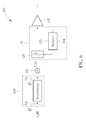
- FIG. 1 is a block diagram of a radio frequency (RF) receiver front-end 100 according to a first embodiment of the invention.
- the receiver front-end 100 is able to fulfill the requirements of low power, high linearity, low noise, and good impedance matching, and can be employed in a low power (or ultra-low power) receiver architecture.
- the receiver front-end 100 can be applied to products based on the Internet of Things (IoT) technology.
- the receiver front-end 100 includes capabilities of gain control to provide different gain settings as well as impedance matching control.
- the receiver front-end 100 is capable of matching with high input impedance of baseband circuits (or intermediate-frequency circuits) by using a mixer-first topology and is also capable of maintaining the high linearity of an amplifier in the open loop by the gain control capability so that no transimpedance amplifiers (TIA) are needed.
- the receiver front-end 100 comprises a mixer 105 such as a passive mixer, a gain control circuit 110, and an amplifier 115.
- the passive mixer 105 such as a voltage mode mixer or a current mode mixer is configured for converting the high or radio frequency input signal S_RF to generate the low frequency signal S_LF.
- the low frequency signal S_LF can be a baseband signal or an intermediate frequency signal.
- the gain control circuit 110 is coupled between an output of passive mixer 105 and an input of amplifier 115.
- the gain control circuit 110 is arranged to detect a signal at the input of amplifier 115 to adjust a gain value that is exerted on the low frequency signal S_LF generated at the output of passive mixer 105.
- the gain control circuit 110 comprises an attenuation circuit 120 and a detector 125.
- the attenuation circuit 120 is coupled between the output of passive mixer 105 and the input of amplifier 115.
- the detector 125 is coupled to the attenuation circuit 120 and the input of amplifier 115, and is used for sensing a level of the signal at the input of amplifier 115 to control the attenuation circuit 120 to adjust/control the gain level to perform gain attenuation for a level of the low frequency signal S_LF.
- the detector 125 is arranged to compare the level of the signal at the input of amplifier 115 with a threshold condition TH to determine whether to adjust the gain value.
- the attenuation circuit 120 is arranged to provide multiple different gain settings. Accordingly, after the process of gain control/adjusting has been completed, the voltage swing at the input of amplifier 115 does not exceed the threshold condition TH, which ensures that the linearity of amplifier 115 will not be degraded.
- the attenuation circuit 120 is also passive for linearity consideration, and the detector 125 is a low-power fast detector as opposed to AGC with ADC which has long settling time.
- the input impedance and output impedance of passive mixer 105 can be configured as high impedances so that the receiver front-end 100 can match with high input impedance of baseband circuits (or intermediate-frequency circuits).
- the circuit size of passive mixer 105 for implementation can be decreased to a smaller one. This achieves that even though a higher turned-on resistance Ron of transistors can still be tolerated as long as the output impedance of the passive mixer 105 is greater than the turned-on resistance Ron.
- this makes a possibility to configure the gain value of an RF matching circuit as a higher value.
- the forward transconductance gain can be configured to be a higher value since output thermal noise contribution becomes smaller due to that the receiver front-end 100 moderately matches with the high input impedance of baseband/intermediate-frequency circuits.
- the gain control circuit 110 is capable of gradually updating and changing (e.g., increasing, decreasing and remaining) the circuit 110 gain value and the threshold condition TH that is used to be compared with the level of the signal at the input of amplifier 115.
- the control can be implemented by analog circuit or digital circuit.. This improves the accuracy of gain control operation as well as maximizing the gain and noise performance without degrading the linearity of the receiver system.
- FIG. 2 is a diagram illustrating a flowchart of an example of operation of gain control circuit 110 as shown in FIG. 1 . Provided that substantially the same result is achieved, the steps of the flowchart shown in FIG. 2 need not be in the exact order shown and need not be contiguous, that is, other steps can be intermediate. Steps are detailed in the following:
- FIG. 3 is diagram illustrating an embodiment of the attenuation circuit 120 shown in FIG. 1 .
- the attenuation circuit 120 comprises a programmable impedance element 1201 including impedance value Z1 that is programmable.
- the programmable impedance element 1201 has one end connected between passive mixer 105 and amplifier 115 and has the other end connected to a ground level.
- the impedance of passive mixer 105 is equal to ZMX, and the input impedance Zin of receiver front-end 100 depends on the impedance value Z1 and is equal to the sum of ZMX and Z1.
- the attenuation circuit 120 for example comprises multiple programmable impedance elements.
- FIG. 4 is diagram illustrating another embodiment of the attenuation circuit 120 shown in FIG. 1 .
- the attenuation circuit 120 comprises a first programmable impedance element 1202 and a second programmable impedance element 1203 that are connected in series.
- the programmable impedance elements 1202 and 1203 include programmable impedance value Z2 and Z3, respectively.
- the programmable impedance element 1202 has one end connected to the output of passive mixer 105 and has the other end connected to the input of amplifier 115, and the programmable impedance element 1203 has one end connected to the input of amplifier 115 and has the other end connected to the ground level.
- the impedance of passive mixer 105 is equal to ZMX, and the input impedance Zin of receiver front-end 100 depends on the impedance value Z2+Z3 and is equal to the sum of ZMX, Z2, and Z3.
- the sum of impedance values Z2 and Z3 can be configured as a constant and fixed value.
- the impedance value Z2 is configured as A ⁇ Z0 and the impedance value Z3 is configured as (1-A) ⁇ Z0 wherein the parameter A is between zero and one and Z0 means a constant value.
- the input impedance Zin of receiver front-end 100 can remain constant while multiple different gain settings are provided.
- FIG. 5 is a diagram illustrating an example of programmable impedance ladder of the attenuation circuit 120 as shown in FIG. 1 .
- the attenuation circuit 120 comprises a programmable impedance ladder 1204 including more impedance elements connected in series and a multiplexer switch 1205.
- the multiplexer switch 1205 is arranged to select one gain setting among multiple different gain settings by selectively connecting the input of amplifier 115 to one node among the intermediate nodes (from n(1) to n(N-1)) based on the detection/control of detector 125 of FIG. 1 .
- N means the total number of impedance elements in the programmable impedance ladder 1204, and Z(k) means the impedance value of k-th impedance element.
- Vo means the voltage at input of the amplifier 115 (that is, the output voltage of passive mixer 105 after processed by the gain control circuit 120), Vi means input voltage of passive mixer 105, parameter s means that the multiplexer switch 1205 connects the input of amplifier 115 to the node between the s-th impedance element and the (s+1)-th impedance element.
- the impedance elements are fixed values in FIG. 5 , it is not meant to be a limitation; in other embodiments, the impedance elements may have programmable impedance values, and similarly, the sum of impedance values of the total number of programmable impedance elements can be also configured as a constant and fixed value such that the input impedance Zin of receiver front-end 100 can remain constant while multiple different gain settings are provided.
- FIG. 6 is block diagram illustrating a radio frequency (RF) receiver front-end 600 according to a second embodiment of the invention.
- the RF receiver front-end 600 comprises a voltage step-up circuit 605, passive mixer 105, gain control circuit 110, and amplifier 115.
- the operations and functions of passive mixer 105, gain control circuit 110, and amplifier 115 are identical to those circuit elements including the same reference numerals in FIG. 1 and are not detailed for brevity.
- the voltage step-up circuit 605 comprising a transformer is used for receiving the high or radio frequency input signal S_RF to provide a voltage gain V5/V4 (that is equal to z 5 z 4 ) for the signal S_RF wherein Z5 means impedance seen from voltage V5 to voltage step-up circuit 605 while Z4 means input impedance seen from voltage V4.
- the voltage step-up circuit 605 is positioned preceding the passive mixer 105.
- the voltage gain is also referred as a step-up ratio.
- the voltage step-up circuit 605 can be implemented by including an inductor L and a capacitor C without using a transformer.
- the combination of inductor L and capacitor C can be also used for providing the voltage gain V5/V4 (that is equal to Z 5 Z 4 ) for the signal S RF.
- V5/V4 that is equal to Z 5 Z 4
- a passive voltage gain can be additionally obtained with low power consumption.
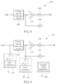
- FIG. 8 is a block diagram of an RF receiver front-end 800 according to a third embodiment of the invention.
- the RF receiver front-end 800 is capable of supporting multiple gain modes to provide gain control for a high or radio frequency input signal S_RF to generate a low frequency signal S_LF as well as providing better impedance matching capability with baseband circuit(s) or intermediate frequency circuit(s). Also, the receiver front-end 800 has lower input return loss and better/improved noise figure.
- Low frequency signal S_LF can be a baseband signal or intermediate frequency signal.
- the receiver front-end 800 comprises a voltage step-up circuit 805, at least one amplifier 810 such as an LNA, at least one first mixer 815, and at least one second mixer 820.
- the voltage step-up circuit 805 is used for receiving a high or radio frequency input signal S_RF and providing a voltage gain (i.e. step-up ratio) for the input signal S_RF.
- the voltage step-up circuit 805 can be implemented by using a transformer as shown in FIG. 6 or a combination of an inductor and a capacitor as shown in FIG. 7 . This is not meant to be a limitation of the invention.
- the LNA 810 is coupled to the output of voltage step-up circuit 805 and to amplify the high or radio frequency input signal S_RF as well as reducing noise.
- the first mixer 815 is coupled to the output of LNA 810 and is used for generating the low frequency signal S_LF in a first gain mode.
- the second mixer 820 is coupled to the output of voltage step-up circuit 805 and is used for generating the low frequency signal S_LF in a gain mode (e.g. second gain mode) different from the first gain mode.
- the voltage step-up circuit 805, LNA 810, and first mixer 815 are enabled in the first gain mode and configured to provide a first gain setting for the input signal S_RF to generate the low frequency signal S_LF.
- the second mixer 820 is disabled.
- the voltage step-up circuit 805 and second mixer 820 are enabled and configured to provide a second gain setting for the input signal S_RF to generate the low frequency signal S_LF, and the LNA 810 and first mixer 815 are disabled.
- the voltage step-up circuit 805 is enabled and employed in both the first and second gain modes. That is, the voltage step-up circuit 805 is shared by both the first mixer 815 and second mixer 820.
- the first gain mode is configured as a higher gain mode providing high gain setting for the signal S_RF to achieve lower noise with an acceptable linearity
- the second gain mode is configured as a low gain mode providing lower gain setting for the signal S_RF to achieve a better linearity performance with acceptable noise.
- the RF receiver front-end 800 can get a good trade-off between noise and linearity performance.
- utilizing the voltage step-up circuit 805 can improve the total gain value of receiver front-end 800 by providing a passive voltage gain (i.e. step-up ratio). Both the above-mentioned gain modes share/use the same voltage step-up circuit 805 to provide multiple gain settings for the input signal S_RF.
- FIG. 9 is a block diagram of an RF receiver front-end 900 according to a fourth embodiment of the invention.
- the receiver front-end 900 includes the capabilities of supporting multiple gain modes to provide gain control for the input signal S_RF and providing better impedance matching with baseband circuit (s) or intermediate frequency circuit(s).
- the receiver 900 comprises the voltage step-up circuit 805, the amplifier 810 such as LNA, first mixer 815, second mixer 820, first switchable impedance unit 825, second switchable impedance unit 830, and a variable impedance unit 835.
- the first switchable impedance unit 825 comprises a switch S1 and a shunt impedance unit Z1
- the second switchable impedance unit 830 comprises a switch S2 and a shunt impedance unit Z2.
- the variable impedance unit 835 comprises a variable/programmable shunt impedance unit Z3.
- the receiver 900 can support three different gain modes to provide three different gain settings for the input signal S_RF, and the voltage step-up circuit 810 is employed in all these three gain modes.
- the three gain modes comprise a high gain mode, a middle gain mode, and a low gain mode.
- the first mixer 815 is coupled to the output of LNA 810 and is used for generating the low frequency signal S_LF in a high gain mode (this can be regarded as a first gain mode).
- the second mixer 820 is coupled to the output of voltage step-up circuit 805 and is used for generating the low frequency signal S_LF in middle and low gain modes (a second gain mode and a third gain mode) that are different from the high gain mode.
- the voltage step-up circuit 805, LNA 810, and first mixer 815 are enabled in the high gain mode and configured to provide a high gain setting for the input signal S_RF to generate the low frequency signal S_LF.
- the second mixer 820 is disabled, and the switches S1 and S2 are open (i.e. disabled) such that the shunt impedance units Z1 and Z2 are disconnected from the voltage step-up circuit 805.
- Voltage step-up circuit 805 can provide a voltage gain for the input signal S_RF, and thus it is not required to configure/implement the LNA 810 with a higher gain value.
- the receiver 900 is arranged to achieve better/excellent noise figure performance with an acceptable linearity performance; that is, the linearity performance can be secondary.
- variable shunt impedance unit Z3 of variable impedance unit 835 is used for impedance matching and gain controls for the signal generate at the output of mixer 815 (i.e. the low frequency signal S_LF).
- the voltage step-up circuit 805 and second mixer 820 are enabled and configured to provide a middle gain setting for the input signal S_RF to generate the low frequency signal S_LF.
- the LNA 810 and first mixer 815 are disabled, and the switches S1 as well as S2 are open (i.e. disabled). Turning off the LNA 810 in the middle gain mode can reduce current consumption.
- the Voltage step-up circuit 805 can provide a voltage gain for the input signal S_RF, and consequently the noise figure of the second mixer 820 can be significantly improved.
- the combination of a voltage step-up circuit and a passive mixer achieves an excellent linearity performance and good noise figure performance.
- the middle gain mode considers a trade-off between noise figure performance and linearity performance.
- the variable shunt impedance unit Z3 of variable impedance unit 835 is used for impedance matching and gain controls for the signal generate at the output of mixer 820 (i.e. the low frequency signal S_LF).
- the voltage step-up circuit 805 and second mixer 820 are enabled, and the switches S1 as well as S2 are closed (i.e. enabled).
- the LNA 810 and first mixer 815 are disabled.
- the voltage step-up circuit 805, second mixer 820, and shunt impedance Z2 are used for providing a low gain setting for the input signal S_RF to generate the low frequency signal S_LF.
- the switch S2 is enabled to reduce the voltage gain (i.e. step-up ratio) provided by voltage step-up circuit 805 by shunting the input of second mixer 820 with the shunt impedance unit Z2.
- enabling the switch S1 is to compensate the input return loss decreased by connecting the shunt impedance Z2 to the receiver front-end 900.
- the input return loss can be improved by shunting the input of voltage step-up circuit 805 with the shunt impedance unit Z1.
- the variable shunt impedance unit Z3 of variable impedance unit 835 is used for impedance matching and gain controls for the signal generate at the output of mixer 820 (i.e. the low frequency signal S_LF).
- the first switchable impedance unit 825 and variable impedance unit 835 can be excluded from the RF receiver front-end 900. That is, RF receiver front-end 900 can comprise only one switchable impedance unit 830 to provide middle gain setting. The first switchable impedance unit 825 and variable impedance unit 835 are optional.
- the voltage step-up circuit 805 may be implemented by using the voltage step-up circuit 605 shown in FIG.6-FIG.7 (e.g. implemented by transformer, LC network or balun), the variable impedance unit 835 may be implemented by the gain control circuit 110 shown in FIG.1-FIG.7 , and the mixer 820 can be passive mixer. If the mixer 820 is implemented by a passive mixer, the variable impedance unit 835 can also be used to adjust the input return loss of the receiver front-end 900.
- FIG. 10 shows a block diagram of an RF receiver front-end that combines the concepts of receiver front-end 100 and receiver front-end 900.
- the receiver front-end 1000 provides impedance matching control and multiple gain modes for gain control while having low power consumption, good input return loss in all gain modes, and good noise figures in both high gain mode and middle gain mode. More specifically, the receiver front-end 1000 uses passive mixer 820 to save current consumption.
- the voltage step-up circuit 805 shared between all gain modes improves noise figures and reduces power consumption as well.
- the switchable impedance unit 825 placed at RF input node improves input return loss.
- the variable impedance unit 835 placed at mixer output node provides impedance matching and additional gain control that ensures the linearity of the amplifier 115. No TIA is required, and the linearity of the receiver chain is maintained with low current consumption.
- the receiver front-end 1000 is therefore suitable for low-power designs or ultra-low-power designs.
- an RF receiver front-end can be configured to comprise a plurality of first mixers, a plurality of second mixers, a plurality of first switchable impedance units, and a plurality of second switchable impedance units wherein the plurality of first switchable impedance units can be optional (not limited).
- FIG. 11 is a block diagram of an RF receiver front-end 1100 according to a fifth embodiment of the invention.
- the receiver front-end 1100 includes capabilities of supporting a variety of gain modes to provide gain control for the input signal S_RF and providing better impedance matching with baseband circuit (s) or intermediate frequency circuit(s).
- the receiver front-end 1100 comprises the voltage step-up circuit 805, multiple amplifier 810A-810B such as LNA, multiple first mixers 815A-815B, multiple second mixers 820A-820B, multiple first switchable impedance units 825A-825B, multiple second switchable impedance units 830A-830B, and the variable impedance unit 835.
- the first switchable impedance units 825A and 825B comprise switches S1a-S1b and shunt impedance units Z1a-Z1b, respectively.
- the second switchable impedance units 830A-830B comprise switches S2a-S2b and shunt impedance units Z2a-Z2b, respectively.
- the variable impedance unit 835 comprises the variable/programmable shunt impedance unit Z3.
- the impedance values of shunt impedance units Z1a-Z1b and shunt impedance units Z2a-Z2b are designed as different (but not limited).
- the receiver front-end 1100 can support more than three different gain modes to provide more than three different gain settings for the input signal S_RF, and the voltage step-up circuit 810 is employed in all these gain modes. For each gain mode, only one among mixers 815A-815B and 820A-820B is enabled, and the other mixers are disabled. Each of switches S2a-S2b can be open or closed to connect or disconnect corresponding one of shunt impedance units Z2a-Z2b, respectively, to provide different gain settings in different gain modes.
- the switch S2a (or S2b) can be open or closed to connect or disconnect corresponding shunt impedance unit Z2a (or Z2b) to the mixer 820A, so as to provide different gain settings.
- the signal S_RF passes through the voltage step-up circuit 805, the LNA 810A and the mixer 815A, and the low frequency signal S_LF is generated with a first gain; in a second gain mode, the signal S_RF passes through the voltage step-up circuit 805, the LNA 810B and the mixer 815B, and the low frequency signal S_LF is generated with a second gain; in a third gain mode, the signal S_RF passes through the voltage step-up circuit 805 and the mixer 820A, and the low frequency signal S_LF is generated with a third gain; in a fourth gain setting, the signal S_RF passes through the voltage step-up circuit 805 having the step-up ratio adjusted by the shunt impedance Z2a and the mixer 820A, and the low frequency signal S_LF is generated with a fourth gain; in a fifth gain setting, the signal S_RF passes through the voltage step-up circuit 805 having the step-up ratio adjusted by the shunt impedance Z2b and the
- the above operation is similar to second mixer 820B. Enabling one of the switches S2a-S2b can reduce the voltage gain (i.e. step-up ratio) provided by voltage step-up circuit 805 by shunting the input of second mixer 820 with one shunt impedance unit. In addition, enabling one of the switches S1a-S1b can improve input return loss by shunting the input of voltage step-up circuit 805 with one shunt impedance unit. Further, in another embodiment, the first switchable impedance units 825A-825B and variable impedance unit 835 can be excluded from the RF receiver front-end 1100.
- RF receiver front-end 1100 can comprise only multiple second switchable impedance units 830A-830B to provide different gain settings.
- First switchable impedance units and variable impedance unit are optional. Additionally, the numbers of first switchable impedance units and second switchable impedance units are not limited. In other embodiments, more than two first switchable impedance units and more than two second switchable impedance units can be employed to provide more gain settings for the input signal S_RF.
- mixers can be implemented by using single-sideband down-conversion mixers, single-balanced mixers, double-balanced mixers, I/Q down-conversion mixers, image-rejection down-conversion mixers, or any combinations.
- the type and selection of mixers are not meant to be a limitation of the invention.
Priority Applications (1)
| Application Number | Priority Date | Filing Date | Title |
|---|---|---|---|
| EP21150080.6A EP3826178A1 (fr) | 2015-09-08 | 2016-09-08 | Récepteur de fréquence radio frontal avec commande de gain ainsi qu'un meilleur contrôle d'adaptation d'impédance |
Applications Claiming Priority (2)
| Application Number | Priority Date | Filing Date | Title |
|---|---|---|---|
| US201562215284P | 2015-09-08 | 2015-09-08 | |
| US15/256,730 US9748993B2 (en) | 2015-09-08 | 2016-09-05 | Radio frequency receiver front-end with gain control capability as well as improved impedance matching control capability |
Related Child Applications (2)
| Application Number | Title | Priority Date | Filing Date |
|---|---|---|---|
| EP21150080.6A Division-Into EP3826178A1 (fr) | 2015-09-08 | 2016-09-08 | Récepteur de fréquence radio frontal avec commande de gain ainsi qu'un meilleur contrôle d'adaptation d'impédance |
| EP21150080.6A Division EP3826178A1 (fr) | 2015-09-08 | 2016-09-08 | Récepteur de fréquence radio frontal avec commande de gain ainsi qu'un meilleur contrôle d'adaptation d'impédance |
Publications (3)
| Publication Number | Publication Date |
|---|---|
| EP3142254A2 true EP3142254A2 (fr) | 2017-03-15 |
| EP3142254A3 EP3142254A3 (fr) | 2017-06-21 |
| EP3142254B1 EP3142254B1 (fr) | 2021-02-17 |
Family
ID=56920520
Family Applications (2)
| Application Number | Title | Priority Date | Filing Date |
|---|---|---|---|
| EP21150080.6A Pending EP3826178A1 (fr) | 2015-09-08 | 2016-09-08 | Récepteur de fréquence radio frontal avec commande de gain ainsi qu'un meilleur contrôle d'adaptation d'impédance |
| EP16187749.3A Active EP3142254B1 (fr) | 2015-09-08 | 2016-09-08 | Récepteur de fréquence radio frontal avec commande de gain ainsi qu'un meilleur contrôle d'adaptation d'impédance |
Family Applications Before (1)
| Application Number | Title | Priority Date | Filing Date |
|---|---|---|---|
| EP21150080.6A Pending EP3826178A1 (fr) | 2015-09-08 | 2016-09-08 | Récepteur de fréquence radio frontal avec commande de gain ainsi qu'un meilleur contrôle d'adaptation d'impédance |
Country Status (3)
| Country | Link |
|---|---|
| US (1) | US9748993B2 (fr) |
| EP (2) | EP3826178A1 (fr) |
| CN (1) | CN106992795B (fr) |
Families Citing this family (12)
| Publication number | Priority date | Publication date | Assignee | Title |
|---|---|---|---|---|
| GB2569714B (en) * | 2016-08-30 | 2022-11-16 | Skyworks Solutions Inc | Multi-input amplifier with programmable embedded attenuators |
| US11881828B2 (en) | 2017-04-04 | 2024-01-23 | Psemi Corporation | Tunable effective inductance for multi-gain LNA with inductive source degeneration |
| US10038418B1 (en) | 2017-04-04 | 2018-07-31 | Psemi Corporation | Optimized multi gain LNA enabling low current and high linearity including highly linear active bypass |
| US20200007098A1 (en) * | 2018-06-29 | 2020-01-02 | Qualcomm Incorporated | Dual-Mode Amplification by Varying a Load Impedance |
| CN111162809B (zh) * | 2019-12-13 | 2022-04-15 | 西安易朴通讯技术有限公司 | 无线接收机及无线设备 |
| CN112511179B (zh) * | 2020-11-02 | 2022-03-22 | 扬州船用电子仪器研究所(中国船舶重工集团公司第七二三研究所) | 一种可重构射频前端接收电路 |
| US11277109B1 (en) * | 2021-02-09 | 2022-03-15 | Psemi Corporation | Disabled input switch for LNA input attenuation |
| FR3120279B1 (fr) * | 2021-02-26 | 2024-01-05 | St Microelectronics Grenoble 2 | Calibration d'un atténuateur RF |
| CN113556090A (zh) * | 2021-07-28 | 2021-10-26 | 深圳昂瑞微电子技术有限公司 | 线性度优化电路以及包括其的低噪声放大器 |
| US11539347B1 (en) * | 2021-09-03 | 2022-12-27 | International Business Machines Corporation | Current-mode frequency translation circuit with programmable gain |
| CN113992234B (zh) * | 2021-12-27 | 2022-03-25 | 智道网联科技(北京)有限公司 | 用于车辆v2x设备的电路、车辆v2x设备以及车辆 |
| CN116015331B (zh) * | 2022-12-26 | 2023-08-08 | 成都爱科特科技发展有限公司 | 一种复杂电磁环境弱信号接收方法、装置及系统 |
Family Cites Families (12)
| Publication number | Priority date | Publication date | Assignee | Title |
|---|---|---|---|---|
| JP2001044861A (ja) | 1999-07-27 | 2001-02-16 | Kyocera Corp | 受信装置 |
| CA2375438A1 (fr) * | 2002-03-08 | 2003-09-08 | Sirific Wireless Corporation | Ameliorations d'un circuit melangeur iq gilbert a linearite elevee |
| CN100517993C (zh) | 2006-04-24 | 2009-07-22 | 中兴通讯股份有限公司 | 一种用于时分双工系统中的多功能收发信机 |
| US8600300B2 (en) * | 2006-12-06 | 2013-12-03 | Broadcom Corporation | Method and system for single chip WLAN and bluetooth radios on a single CMOS substrate |
| US7599675B2 (en) * | 2006-12-12 | 2009-10-06 | Telefonaktiebolaget Lm Ericsson (Publ) | Method and apparatus for receiving radio frequency signals |
| CN101641929A (zh) * | 2007-01-26 | 2010-02-03 | 新加坡科技研究局 | 射频识别收发器 |
| US8639205B2 (en) | 2008-03-20 | 2014-01-28 | Qualcomm Incorporated | Reduced power-consumption receivers |
| US8433272B2 (en) * | 2008-04-15 | 2013-04-30 | Qualcomm Incorporated | Reconfigurable high linearity low noise figure receiver requiring no interstage saw filter |
| US8351978B2 (en) * | 2008-08-01 | 2013-01-08 | Aleksandar Tasic | Systems and methods for adjusting the gain of a receiver through a gain tuning network |
| US8086208B2 (en) | 2008-12-05 | 2011-12-27 | Passif Semiconductor Corp. | Passive wireless receiver |
| CN102664653B (zh) * | 2012-05-17 | 2014-09-03 | 天津里外科技有限公司 | 移动终端及其具有射频数模转换式线性发射机的射频前端 |
| US9548709B2 (en) | 2012-12-19 | 2017-01-17 | Qualcomm Incorporated | Independent gain control for multiple receive circuits concurrently processing different transmitted signals |
-
2016
- 2016-09-05 US US15/256,730 patent/US9748993B2/en active Active
- 2016-09-08 EP EP21150080.6A patent/EP3826178A1/fr active Pending
- 2016-09-08 CN CN201610810277.XA patent/CN106992795B/zh active Active
- 2016-09-08 EP EP16187749.3A patent/EP3142254B1/fr active Active
Non-Patent Citations (1)
| Title |
|---|
| None |
Also Published As
| Publication number | Publication date |
|---|---|
| EP3142254B1 (fr) | 2021-02-17 |
| US9748993B2 (en) | 2017-08-29 |
| CN106992795B (zh) | 2019-04-26 |
| EP3142254A3 (fr) | 2017-06-21 |
| CN106992795A (zh) | 2017-07-28 |
| US20170070252A1 (en) | 2017-03-09 |
| EP3826178A1 (fr) | 2021-05-26 |
Similar Documents
| Publication | Publication Date | Title |
|---|---|---|
| EP3142254B1 (fr) | Récepteur de fréquence radio frontal avec commande de gain ainsi qu'un meilleur contrôle d'adaptation d'impédance | |
| US10193583B2 (en) | Radio frequency tuner | |
| US10205438B2 (en) | Adjustable low-pass filter in a compact low-power receiver | |
| KR101125492B1 (ko) | 증폭기를 위한 구성가능한 피드백 | |
| US8331895B2 (en) | Receiving circuit | |
| US7332967B2 (en) | Variable gain amplifier with low phase variation | |
| US9166632B1 (en) | Mixer circuits with programmable characteristics | |
| US20050276358A1 (en) | Wireless LAN receiver with I and Q RF and baseband AGC loops and DC offset cancellation | |
| JP6278281B2 (ja) | ミキサ回路 | |
| EP0969601B1 (fr) | Procedé d'amélioration d'un signal utile dans un récepteur radio | |
| US9496906B2 (en) | Receiver with wide gain range | |
| WO2014080586A1 (fr) | Amplificateur à gain variable et système de syntonisateur l'intégrant | |
| EP3278459A1 (fr) | Réception d'une pluralité de bandes radiofréquence | |
| KR100882406B1 (ko) | 재구성가능한 주파수 필터 | |
| US8816750B2 (en) | High frequency mixer with tunable dynamic range | |
| US9673769B2 (en) | Variable gain circuit and tuner system provided with same | |
| EP1608061A1 (fr) | Convertisseur de fréquence utilisant un filtre bandpassante accordable | |
| US20050070240A1 (en) | Receiver device comprising an alternating current coupling | |
| US20220345170A1 (en) | Bias circuit for a low noise amplifier of a front end interface of a radio frequency communication device that enables fast transitions between different operating modes | |
| JP3315948B2 (ja) | 無線装置とその利得の制御方法 | |
| JP2007324918A (ja) | アンテナアッテネータ回路 |
Legal Events
| Date | Code | Title | Description |
|---|---|---|---|
| PUAI | Public reference made under article 153(3) epc to a published international application that has entered the european phase |
Free format text: ORIGINAL CODE: 0009012 |
|
| STAA | Information on the status of an ep patent application or granted ep patent |
Free format text: STATUS: THE APPLICATION HAS BEEN PUBLISHED |
|
| AK | Designated contracting states |
Kind code of ref document: A2 Designated state(s): AL AT BE BG CH CY CZ DE DK EE ES FI FR GB GR HR HU IE IS IT LI LT LU LV MC MK MT NL NO PL PT RO RS SE SI SK SM TR |
|
| AX | Request for extension of the european patent |
Extension state: BA ME |
|
| PUAL | Search report despatched |
Free format text: ORIGINAL CODE: 0009013 |
|
| AK | Designated contracting states |
Kind code of ref document: A3 Designated state(s): AL AT BE BG CH CY CZ DE DK EE ES FI FR GB GR HR HU IE IS IT LI LT LU LV MC MK MT NL NO PL PT RO RS SE SI SK SM TR |
|
| AX | Request for extension of the european patent |
Extension state: BA ME |
|
| RIC1 | Information provided on ipc code assigned before grant |
Ipc: H04B 1/30 20060101ALI20170515BHEP Ipc: H03G 3/30 20060101AFI20170515BHEP |
|
| STAA | Information on the status of an ep patent application or granted ep patent |
Free format text: STATUS: REQUEST FOR EXAMINATION WAS MADE |
|
| 17P | Request for examination filed |
Effective date: 20171219 |
|
| RBV | Designated contracting states (corrected) |
Designated state(s): AL AT BE BG CH CY CZ DE DK EE ES FI FR GB GR HR HU IE IS IT LI LT LU LV MC MK MT NL NO PL PT RO RS SE SI SK SM TR |
|
| STAA | Information on the status of an ep patent application or granted ep patent |
Free format text: STATUS: EXAMINATION IS IN PROGRESS |
|
| 17Q | First examination report despatched |
Effective date: 20191121 |
|
| RIC1 | Information provided on ipc code assigned before grant |
Ipc: H04B 1/30 20060101ALI20200731BHEP Ipc: H03D 7/14 20060101ALI20200731BHEP Ipc: H03G 3/30 20060101AFI20200731BHEP Ipc: H04B 1/16 20060101ALI20200731BHEP Ipc: H04B 1/40 20150101ALI20200731BHEP |
|
| GRAP | Despatch of communication of intention to grant a patent |
Free format text: ORIGINAL CODE: EPIDOSNIGR1 |
|
| STAA | Information on the status of an ep patent application or granted ep patent |
Free format text: STATUS: GRANT OF PATENT IS INTENDED |
|
| INTG | Intention to grant announced |
Effective date: 20200911 |
|
| GRAS | Grant fee paid |
Free format text: ORIGINAL CODE: EPIDOSNIGR3 |
|
| GRAA | (expected) grant |
Free format text: ORIGINAL CODE: 0009210 |
|
| STAA | Information on the status of an ep patent application or granted ep patent |
Free format text: STATUS: THE PATENT HAS BEEN GRANTED |
|
| AK | Designated contracting states |
Kind code of ref document: B1 Designated state(s): AL AT BE BG CH CY CZ DE DK EE ES FI FR GB GR HR HU IE IS IT LI LT LU LV MC MK MT NL NO PL PT RO RS SE SI SK SM TR |
|
| REG | Reference to a national code |
Ref country code: GB Ref legal event code: FG4D |
|
| REG | Reference to a national code |
Ref country code: CH Ref legal event code: EP |
|
| REG | Reference to a national code |
Ref country code: DE Ref legal event code: R096 Ref document number: 602016052486 Country of ref document: DE |
|
| REG | Reference to a national code |
Ref country code: AT Ref legal event code: REF Ref document number: 1362837 Country of ref document: AT Kind code of ref document: T Effective date: 20210315 |
|
| REG | Reference to a national code |
Ref country code: IE Ref legal event code: FG4D |
|
| REG | Reference to a national code |
Ref country code: LT Ref legal event code: MG9D |
|
| REG | Reference to a national code |
Ref country code: NL Ref legal event code: MP Effective date: 20210217 |
|
| PG25 | Lapsed in a contracting state [announced via postgrant information from national office to epo] |
Ref country code: PT Free format text: LAPSE BECAUSE OF FAILURE TO SUBMIT A TRANSLATION OF THE DESCRIPTION OR TO PAY THE FEE WITHIN THE PRESCRIBED TIME-LIMIT Effective date: 20210617 Ref country code: NO Free format text: LAPSE BECAUSE OF FAILURE TO SUBMIT A TRANSLATION OF THE DESCRIPTION OR TO PAY THE FEE WITHIN THE PRESCRIBED TIME-LIMIT Effective date: 20210517 Ref country code: LT Free format text: LAPSE BECAUSE OF FAILURE TO SUBMIT A TRANSLATION OF THE DESCRIPTION OR TO PAY THE FEE WITHIN THE PRESCRIBED TIME-LIMIT Effective date: 20210217 Ref country code: FI Free format text: LAPSE BECAUSE OF FAILURE TO SUBMIT A TRANSLATION OF THE DESCRIPTION OR TO PAY THE FEE WITHIN THE PRESCRIBED TIME-LIMIT Effective date: 20210217 Ref country code: GR Free format text: LAPSE BECAUSE OF FAILURE TO SUBMIT A TRANSLATION OF THE DESCRIPTION OR TO PAY THE FEE WITHIN THE PRESCRIBED TIME-LIMIT Effective date: 20210518 Ref country code: HR Free format text: LAPSE BECAUSE OF FAILURE TO SUBMIT A TRANSLATION OF THE DESCRIPTION OR TO PAY THE FEE WITHIN THE PRESCRIBED TIME-LIMIT Effective date: 20210217 Ref country code: BG Free format text: LAPSE BECAUSE OF FAILURE TO SUBMIT A TRANSLATION OF THE DESCRIPTION OR TO PAY THE FEE WITHIN THE PRESCRIBED TIME-LIMIT Effective date: 20210517 |
|
| REG | Reference to a national code |
Ref country code: AT Ref legal event code: MK05 Ref document number: 1362837 Country of ref document: AT Kind code of ref document: T Effective date: 20210217 |
|
| PG25 | Lapsed in a contracting state [announced via postgrant information from national office to epo] |
Ref country code: SE Free format text: LAPSE BECAUSE OF FAILURE TO SUBMIT A TRANSLATION OF THE DESCRIPTION OR TO PAY THE FEE WITHIN THE PRESCRIBED TIME-LIMIT Effective date: 20210217 Ref country code: NL Free format text: LAPSE BECAUSE OF FAILURE TO SUBMIT A TRANSLATION OF THE DESCRIPTION OR TO PAY THE FEE WITHIN THE PRESCRIBED TIME-LIMIT Effective date: 20210217 Ref country code: LV Free format text: LAPSE BECAUSE OF FAILURE TO SUBMIT A TRANSLATION OF THE DESCRIPTION OR TO PAY THE FEE WITHIN THE PRESCRIBED TIME-LIMIT Effective date: 20210217 Ref country code: RS Free format text: LAPSE BECAUSE OF FAILURE TO SUBMIT A TRANSLATION OF THE DESCRIPTION OR TO PAY THE FEE WITHIN THE PRESCRIBED TIME-LIMIT Effective date: 20210217 Ref country code: PL Free format text: LAPSE BECAUSE OF FAILURE TO SUBMIT A TRANSLATION OF THE DESCRIPTION OR TO PAY THE FEE WITHIN THE PRESCRIBED TIME-LIMIT Effective date: 20210217 |
|
| PG25 | Lapsed in a contracting state [announced via postgrant information from national office to epo] |
Ref country code: IS Free format text: LAPSE BECAUSE OF FAILURE TO SUBMIT A TRANSLATION OF THE DESCRIPTION OR TO PAY THE FEE WITHIN THE PRESCRIBED TIME-LIMIT Effective date: 20210617 |
|
| PG25 | Lapsed in a contracting state [announced via postgrant information from national office to epo] |
Ref country code: EE Free format text: LAPSE BECAUSE OF FAILURE TO SUBMIT A TRANSLATION OF THE DESCRIPTION OR TO PAY THE FEE WITHIN THE PRESCRIBED TIME-LIMIT Effective date: 20210217 Ref country code: CZ Free format text: LAPSE BECAUSE OF FAILURE TO SUBMIT A TRANSLATION OF THE DESCRIPTION OR TO PAY THE FEE WITHIN THE PRESCRIBED TIME-LIMIT Effective date: 20210217 Ref country code: AT Free format text: LAPSE BECAUSE OF FAILURE TO SUBMIT A TRANSLATION OF THE DESCRIPTION OR TO PAY THE FEE WITHIN THE PRESCRIBED TIME-LIMIT Effective date: 20210217 Ref country code: SM Free format text: LAPSE BECAUSE OF FAILURE TO SUBMIT A TRANSLATION OF THE DESCRIPTION OR TO PAY THE FEE WITHIN THE PRESCRIBED TIME-LIMIT Effective date: 20210217 |
|
| REG | Reference to a national code |
Ref country code: DE Ref legal event code: R097 Ref document number: 602016052486 Country of ref document: DE |
|
| PG25 | Lapsed in a contracting state [announced via postgrant information from national office to epo] |
Ref country code: ES Free format text: LAPSE BECAUSE OF FAILURE TO SUBMIT A TRANSLATION OF THE DESCRIPTION OR TO PAY THE FEE WITHIN THE PRESCRIBED TIME-LIMIT Effective date: 20210217 Ref country code: DK Free format text: LAPSE BECAUSE OF FAILURE TO SUBMIT A TRANSLATION OF THE DESCRIPTION OR TO PAY THE FEE WITHIN THE PRESCRIBED TIME-LIMIT Effective date: 20210217 Ref country code: SK Free format text: LAPSE BECAUSE OF FAILURE TO SUBMIT A TRANSLATION OF THE DESCRIPTION OR TO PAY THE FEE WITHIN THE PRESCRIBED TIME-LIMIT Effective date: 20210217 Ref country code: RO Free format text: LAPSE BECAUSE OF FAILURE TO SUBMIT A TRANSLATION OF THE DESCRIPTION OR TO PAY THE FEE WITHIN THE PRESCRIBED TIME-LIMIT Effective date: 20210217 |
|
| PLBE | No opposition filed within time limit |
Free format text: ORIGINAL CODE: 0009261 |
|
| STAA | Information on the status of an ep patent application or granted ep patent |
Free format text: STATUS: NO OPPOSITION FILED WITHIN TIME LIMIT |
|
| 26N | No opposition filed |
Effective date: 20211118 |
|
| PG25 | Lapsed in a contracting state [announced via postgrant information from national office to epo] |
Ref country code: AL Free format text: LAPSE BECAUSE OF FAILURE TO SUBMIT A TRANSLATION OF THE DESCRIPTION OR TO PAY THE FEE WITHIN THE PRESCRIBED TIME-LIMIT Effective date: 20210217 |
|
| PG25 | Lapsed in a contracting state [announced via postgrant information from national office to epo] |
Ref country code: SI Free format text: LAPSE BECAUSE OF FAILURE TO SUBMIT A TRANSLATION OF THE DESCRIPTION OR TO PAY THE FEE WITHIN THE PRESCRIBED TIME-LIMIT Effective date: 20210217 |
|
| PG25 | Lapsed in a contracting state [announced via postgrant information from national office to epo] |
Ref country code: IT Free format text: LAPSE BECAUSE OF FAILURE TO SUBMIT A TRANSLATION OF THE DESCRIPTION OR TO PAY THE FEE WITHIN THE PRESCRIBED TIME-LIMIT Effective date: 20210217 |
|
| REG | Reference to a national code |
Ref country code: CH Ref legal event code: PL |
|
| REG | Reference to a national code |
Ref country code: BE Ref legal event code: MM Effective date: 20210930 |
|
| PG25 | Lapsed in a contracting state [announced via postgrant information from national office to epo] |
Ref country code: IS Free format text: LAPSE BECAUSE OF FAILURE TO SUBMIT A TRANSLATION OF THE DESCRIPTION OR TO PAY THE FEE WITHIN THE PRESCRIBED TIME-LIMIT Effective date: 20210617 Ref country code: MC Free format text: LAPSE BECAUSE OF FAILURE TO SUBMIT A TRANSLATION OF THE DESCRIPTION OR TO PAY THE FEE WITHIN THE PRESCRIBED TIME-LIMIT Effective date: 20210217 |
|
| PG25 | Lapsed in a contracting state [announced via postgrant information from national office to epo] |
Ref country code: LU Free format text: LAPSE BECAUSE OF NON-PAYMENT OF DUE FEES Effective date: 20210908 Ref country code: IE Free format text: LAPSE BECAUSE OF NON-PAYMENT OF DUE FEES Effective date: 20210908 Ref country code: BE Free format text: LAPSE BECAUSE OF NON-PAYMENT OF DUE FEES Effective date: 20210930 |
|
| PG25 | Lapsed in a contracting state [announced via postgrant information from national office to epo] |
Ref country code: LI Free format text: LAPSE BECAUSE OF NON-PAYMENT OF DUE FEES Effective date: 20210930 Ref country code: CH Free format text: LAPSE BECAUSE OF NON-PAYMENT OF DUE FEES Effective date: 20210930 |
|
| PG25 | Lapsed in a contracting state [announced via postgrant information from national office to epo] |
Ref country code: HU Free format text: LAPSE BECAUSE OF FAILURE TO SUBMIT A TRANSLATION OF THE DESCRIPTION OR TO PAY THE FEE WITHIN THE PRESCRIBED TIME-LIMIT; INVALID AB INITIO Effective date: 20160908 |
|
| PG25 | Lapsed in a contracting state [announced via postgrant information from national office to epo] |
Ref country code: CY Free format text: LAPSE BECAUSE OF FAILURE TO SUBMIT A TRANSLATION OF THE DESCRIPTION OR TO PAY THE FEE WITHIN THE PRESCRIBED TIME-LIMIT Effective date: 20210217 |
|
| P01 | Opt-out of the competence of the unified patent court (upc) registered |
Effective date: 20230607 |
|
| PGFP | Annual fee paid to national office [announced via postgrant information from national office to epo] |
Ref country code: GB Payment date: 20230927 Year of fee payment: 8 |
|
| PGFP | Annual fee paid to national office [announced via postgrant information from national office to epo] |
Ref country code: FR Payment date: 20230925 Year of fee payment: 8 Ref country code: DE Payment date: 20230927 Year of fee payment: 8 |