EP3129798B1 - Rücksetzungsschema für abtastketten mit asynchronen rücksetzungssignalen - Google Patents
Rücksetzungsschema für abtastketten mit asynchronen rücksetzungssignalen Download PDFInfo
- Publication number
- EP3129798B1 EP3129798B1 EP15713279.6A EP15713279A EP3129798B1 EP 3129798 B1 EP3129798 B1 EP 3129798B1 EP 15713279 A EP15713279 A EP 15713279A EP 3129798 B1 EP3129798 B1 EP 3129798B1
- Authority
- EP
- European Patent Office
- Prior art keywords
- scan
- reset
- state
- flip
- type
- Prior art date
- Legal status (The legal status is an assumption and is not a legal conclusion. Google has not performed a legal analysis and makes no representation as to the accuracy of the status listed.)
- Active
Links
- 238000000034 method Methods 0.000 claims description 58
- 238000010586 diagram Methods 0.000 description 21
- 230000008901 benefit Effects 0.000 description 5
- 238000013461 design Methods 0.000 description 4
- 238000012938 design process Methods 0.000 description 3
- 230000006870 function Effects 0.000 description 3
- 238000004519 manufacturing process Methods 0.000 description 3
- 238000013459 approach Methods 0.000 description 2
- 238000012986 modification Methods 0.000 description 1
- 230000004048 modification Effects 0.000 description 1
- 238000012545 processing Methods 0.000 description 1
- 238000003672 processing method Methods 0.000 description 1
- 238000012360 testing method Methods 0.000 description 1
Images






Classifications
-
- G—PHYSICS
- G01—MEASURING; TESTING
- G01R—MEASURING ELECTRIC VARIABLES; MEASURING MAGNETIC VARIABLES
- G01R31/00—Arrangements for testing electric properties; Arrangements for locating electric faults; Arrangements for electrical testing characterised by what is being tested not provided for elsewhere
- G01R31/28—Testing of electronic circuits, e.g. by signal tracer
- G01R31/317—Testing of digital circuits
- G01R31/3181—Functional testing
- G01R31/3185—Reconfiguring for testing, e.g. LSSD, partitioning
- G01R31/318533—Reconfiguring for testing, e.g. LSSD, partitioning using scanning techniques, e.g. LSSD, Boundary Scan, JTAG
- G01R31/318536—Scan chain arrangements, e.g. connections, test bus, analog signals
-
- H—ELECTRICITY
- H03—ELECTRONIC CIRCUITRY
- H03K—PULSE TECHNIQUE
- H03K3/00—Circuits for generating electric pulses; Monostable, bistable or multistable circuits
- H03K3/01—Details
- H03K3/012—Modifications of generator to improve response time or to decrease power consumption
-
- G—PHYSICS
- G01—MEASURING; TESTING
- G01R—MEASURING ELECTRIC VARIABLES; MEASURING MAGNETIC VARIABLES
- G01R31/00—Arrangements for testing electric properties; Arrangements for locating electric faults; Arrangements for electrical testing characterised by what is being tested not provided for elsewhere
- G01R31/28—Testing of electronic circuits, e.g. by signal tracer
- G01R31/317—Testing of digital circuits
- G01R31/3181—Functional testing
- G01R31/3185—Reconfiguring for testing, e.g. LSSD, partitioning
- G01R31/318533—Reconfiguring for testing, e.g. LSSD, partitioning using scanning techniques, e.g. LSSD, Boundary Scan, JTAG
- G01R31/318541—Scan latches or cell details
-
- G—PHYSICS
- G01—MEASURING; TESTING
- G01R—MEASURING ELECTRIC VARIABLES; MEASURING MAGNETIC VARIABLES
- G01R31/00—Arrangements for testing electric properties; Arrangements for locating electric faults; Arrangements for electrical testing characterised by what is being tested not provided for elsewhere
- G01R31/28—Testing of electronic circuits, e.g. by signal tracer
- G01R31/317—Testing of digital circuits
- G01R31/3181—Functional testing
- G01R31/3185—Reconfiguring for testing, e.g. LSSD, partitioning
- G01R31/318533—Reconfiguring for testing, e.g. LSSD, partitioning using scanning techniques, e.g. LSSD, Boundary Scan, JTAG
- G01R31/318594—Timing aspects
-
- G—PHYSICS
- G11—INFORMATION STORAGE
- G11C—STATIC STORES
- G11C19/00—Digital stores in which the information is moved stepwise, e.g. shift registers
- G11C19/34—Digital stores in which the information is moved stepwise, e.g. shift registers using storage elements with more than two stable states represented by steps, e.g. of voltage, current, phase, frequency
-
- H—ELECTRICITY
- H03—ELECTRONIC CIRCUITRY
- H03K—PULSE TECHNIQUE
- H03K3/00—Circuits for generating electric pulses; Monostable, bistable or multistable circuits
- H03K3/02—Generators characterised by the type of circuit or by the means used for producing pulses
- H03K3/027—Generators characterised by the type of circuit or by the means used for producing pulses by the use of logic circuits, with internal or external positive feedback
- H03K3/037—Bistable circuits
- H03K3/0375—Bistable circuits provided with means for increasing reliability; for protection; for ensuring a predetermined initial state when the supply voltage has been applied; for storing the actual state when the supply voltage fails
Definitions
- the present disclosure relates generally to scan chains, and more particularly, to an asynchronous reset scheme for scan chains with asynchronous reset signals.
- set/reset flip-flops are used in scan chains within a memory in a system on chip (SoC).
- SoC system on chip
- set/reset flip-flops are 10% larger than non-set/non-reset flip-flops.
- the larger flip-flops affect the area, power consumption, and speed of operation of the SoC. Accordingly, apparatuses and methods are needed for using non-set/non-reset flip-flops in scan chains in association with asynchronous resets of the scan chains.
- document CN 103 023 467 A which relates to to the technical field of scan chain reset signal processing, and in particular relates to a processing method of a reset port of a scan chain asynchronous rest register, comprising a register group which asynchronously resets and adopts a combinational logic circuit to generate resetting signals.
- the register resetting method comprises the following steps of: (1) constructing scan chains for all registers, respectively connecting data input ends and data output ends of the registers in the scan chains with a not gate, wherein the registers need to be reset to 1; and (2) continuously inputting a reset value 0 to the head of the scan chain.
- the register resetting device comprises a resetting control logic and a clock control logic which are respectively connected with each register; the register resetting device also comprises reset value converting units, the number of which is in one to one correspondence with the number of the registers needing to be reset to 1.
- an apparatus comprising at least one scan chain, as set forth in claim 1, and a method for performing an asynchronous reset in an apparatus including at least one scan chain, as set forth in claim 2, is provided.
- flip-flops have a set pin, a reset pin, or both set and reset pins. Enabling the set pin forces the flip-flop to store a 1. Enabling the reset pin forces the flip-flop to store a 0.
- Flip-flops having the ability to be set or reset by a set or reset signal include circuitry that performs the set or reset.
- the exemplary methods/apparatuses use a different approach to force the output of a flip-flop to a desired state. Rather than setting or resetting all flip-flops using a set or reset pin upon a reset, a desired state is clocked into the flip-flops using a scan chain, and subsequently, the inverse state is set or reset (using the built-in set/reset circuitry) into the flip-flops that are required to store the inverse state upon the reset.
- Flip-flops that are supposed to be reset to the desired state are designed/constructed/manufactured to be non-set/non-reset flip-flops, and flip-flops that are supposed to be reset to store the inverse state are designed/constructed/manufactured to be reset type flip-flops (with built-in reset functionality) or set type flip-flops (with built-in set functionality).
- Set type flip-flops have built-in set functionality/circuitry for setting a 1 state into the flip-flop, and reset type flip-flops have built-in reset functionality/circuitry for resetting the state of the flip-flop to a 0.
- Non-set/non-reset flip-flops do not have such built-in set/reset functionality, and must be reset to a particular state by clocking the particular state into the flip-flop so that the state is stored in the flip-flop.
- Flip-flops without the set/reset functionality consume less area and power than traditional flip-flops having a set function, reset function, or both.
- FIG. 1 is a diagram 100 illustrating an exemplary reset controller 102 and a memory/core 104.
- FIG. 2 is an exemplary timing diagram 200 associated with the reset controller 102 and the memory/core 104.
- the reset controller 102 (also referred to as a reset module) is configured to reset scan chains in the memory/core 104 upon a power on reset (POR) when being powered on, a watchdog reset in which a reset is due to the expiration of a watch dog timer (e.g., due to a software issue), a soft reset by software due to a software issue or a need to re-initialize the system after a particular operation, or a wake up reset after a power down of one or more modules.
- POR power on reset
- a watchdog reset in which a reset is due to the expiration of a watch dog timer (e.g., due to a software issue)
- a soft reset by software due to a software issue or a need to re-initial
- the reset controller 102 controls the scan_enable, the scan_in, and the clock during a reset phase of the memory/core 104. As shown in FIG. 2 , the reset controller 102 sets the state of the scan_in to a high state or a low state (shown in FIG. 2 as a low state) and enables the scan_enable. In one configuration, the controller then clocks/shifts the state at the scan_in through all of the scan cells within the memory/core 104. In addition, if particular scan cells need to be reset/set to an opposite state than the state clocked/shifted through the scan cells, the reset controller 102 enables the async_set/reset and sets/resets the particular scan cells within the memory/core 104 that need to be reset/set.
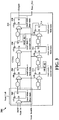
- FIG. 3 is a first diagram 300 illustrating a first apparatus and method associated with an asynchronous reset scheme for scan chains.
- the memory/core 320 includes a scan chain.
- the scan chain includes a plurality of scan cells coupled together.
- Each scan cell includes a multiplexer and a flip-flop.
- Flip-flops that need to be reset to a first state s are configured (e.g., designed and manufactured/constructed) to be non-set/non-reset flip-flops and flip-flops that need to be reset to a second state s are configured (e.g., designed and manufactured/constructed) to be set/reset flip-flops.
- the flip-flops 302, 304, 308, 312, and 314 need to be reset to a first state s and are therefore non-set/non-reset flip-flops.
- the flip-flops 306 and 310 need to be reset to a second state s and are therefore set/reset flip-flops.
- flip-flops that need to be reset to a 0 are configured to be non-set/non-reset flip-flops
- flip-flops that need to be reset to a 1 are configured to be set/reset flip-flops.
- the reset controller 102 inputs a 0 at the scan_in, enables the scan_enable to select the scan_in input at the multiplexer, and clocks/shifts a 0 through each of the flip-flops 302-314 until a 0 is stored in each of the flip-flops 302-314.
- the reset controller 102 sets a 1 into the flip-flops 306 and 310 (at a set pin labeled as "SR" using the built-in set functionality/circuitry in the flip-flop).
- flip-flops that need to be reset to a 1 are configured to be non-set/non-reset flip-flops
- flip-flops that need to be reset to a 0 are configured to be set/reset flip-flops.
- the reset controller 102 inputs a 1 at the scan_in, enables the scan_enable to select the scan_in input at the multiplexer, and clocks/shifts a 1 through each of the flip-flops 302-314 until a 1 is stored in each of the flip-flops 302-314. Subsequently, the reset controller 102 resets the flip-flops 306 and 310 to store a 0 (at a reset pin labeled as "SR" using the built-in reset functionality/circuitry in the flip-flop).
- an apparatus e.g., a memory
- Each of the at least one scan chain includes a plurality of scan cells coupled together.
- Each scan cell in the at least one scan chain includes a first type of scan cell when a reset state of the scan cell is a first state s , and a second type of scan cell different than the first type of scan cell when the reset state of the scan cell is a second state s .
- One or more scan chains of the at least one scan chain includes at least one of the first type of scan cell and at least one of the second type of scan cell.
- the first type of scan cell includes a multiplexer coupled to a first-type flip-flop without both set and reset functionality (e.g., the flip-flops 302, 304, 308, 312, and 314) (i.e., the first-type flip-flop does not contain set functionality and does not contain reset functionality), and the second type of scan cell includes a multiplexer coupled to a second-type flip-flop with at least one of set or reset functionality (e.g., the flip-flops 306 and 310).
- the second-type flip-flop includes set functionality.
- the reset controller 102 is configured to input the first state 0 into each of the at least one scan chain; to start a clock to clock the first state 0 through the scan cells until each flip-flop (including both first-type flip-flops and second-type flip-flops) in the at least one scan chain stores the first state 0; to stop the clock; and to set, subsequent to stopping the clock, the second state 1 into each of the second-type flip-flops within the at least one scan chain.
- Inputting the first state 0 into each of the at least one scan chain is a serial process.
- Setting the second state 1 into each of the second-type flip-flops within the at least one scan chain is a parallel process.
- the at least one scan chain is reset asynchronously by storing the first state in a serially process in both the first-type flip-flops and the second-type flip-flops, and subsequently, storing (through a set) the second state in a parallel process in the second-type flip-flops.
- the reset controller 102 is configured to input the first state 1 into each of the at least one scan chain; to start a clock to clock the first state 1 through the scan cells until each flip-flop (including both first-type flip-flops and second-type flip-flops) in the at least one scan chain stores the first state 1; to stop the clock; and to reset, subsequent to stopping the clock, each of the second-type flip-flops within the at least one scan chain to store the second state 0.
- Inputting the first state 1 into each of the at least one scan chain is a serial process.
- Resetting the second-type flip-flops within the at least one scan chain to store the second state 0 is a parallel process.
- the at least one scan chain is reset asynchronously by storing the first state in a serially process in both the first-type flip-flops and the second-type flip-flops, and subsequently, storing (through a reset) the second state in a parallel process in the second-type flip-flops.
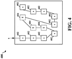
- FIG. 4 is a second diagram 400 illustrating the first apparatus and method associated with an asynchronous reset scheme for scan chains.
- a scan chain includes scan cells coupled together. Some of the scan cells include flip-flops 402 without reset/set functionality, and some of the scan cells include flip-flops 404 with reset/set functionality.
- the scan cells that need to be reset to the state s are configured to include non-reset/non-set flip-flops 402 and the scan cells that need to be reset to the state s are configured to include reset/set flip-flops 404.
- the non-reset/non-set flip-flops in a scan chain requires a longer reset period for clocking a particular state through each of the flip-flops in the scan chain (if only reset/set flip-flops are used, they all may be reset/set at the same time).
- the non-reset/non-set flip-flops are 10% smaller than reset/set flip-flops, use less power than reset/set flip-flops, and are faster than reset/set flip-flops, the first apparatus and method reduces an area, power consumption, and speed of operation of the scan cells by utilizing non-reset/non-set flip-flops in some of the scan cells.
- non-reset/non-set flip-flops are less susceptible than set/reset flip-flops during near threshold computing (NTC) operation. Use of the non-reset/non-set flip-flops would therefore allow the use of a lower operating voltage during NTC operation than may be used when using reset/set flip-flops during NTC operation. In addition, use of non-reset/non-set flip-flops may save routing overhead for the reset/set pins. Lastly, no reset control is required during a design for test (DFT) (also known as design for testability) when using non-reset/non-set flip-flops.
- DFT design for test
- FIG. 5 is a first diagram 500 illustrating a second exemplary apparatus and method associated with an asynchronous reset scheme for scan chains.
- the memory/core 520 includes two scan chains 502 and 504.
- a first scan chain 502 has a reset state of a first state s
- a second scan chain 504 has a reset state of a second state s .
- scan cells that have a reset state of a first state s are linked together (e.g., in the design and manufacturing process) into one or more scan chains
- scan cells that have a reset state of a second state s are linked together (e.g., in the design and manufacturing process) into one or more scan chains.
- all flip-flops may be configured to be non-reset/non-set flip-flops.
- the reset controller 102 may then shift/clock the first state s through the scan chains that have a reset state of a first state s and shift/clock the second state s through the scan chains that have a reset state of a second state s .
- an apparatus includes a first set of scan chains 502 including flip-flops without both set and reset functionality. Each of the flip-flops in the first set of scan chains 502 has a reset state of a first state s .
- the apparatus includes a second set of scan chains 504 including flip-flops without both set and reset functionality. Each of the flip-flops in the second set of scan chains 504 has the reset state of a second state s different than the first state s .
- a reset module e.g., the reset controller 102 is configured to clock a first state s into each flip-flop in the first set of scan chains and to clock a second state s different than the first state s into each flip-flop in the second set of scan chains.
- the reset module is configured to asynchronously reset the first set of scan chains 502 by inputting the first state s into each scan chain (at the scan-in) in the first set of scan chains 502 and clocking the first state s through the flip-flops until each flip-flop in the first set of scan chains 502 stores the first state s .
- the reset module is configured to asynchronously reset the second set of scan chains 504 by inputting the second state s into each scan chain (at the scan_in) in the second set of scan chains 504 and clocking the second state s through the flip-flops until each flip-flop in the second set of scan chains 504 stores the second state s .
- the first and second states s , s are 0 and 1, respectively.
- the first and second states s , s are 1 and 0, respectively.
- FIG. 6 is a second diagram 600 illustrating the second exemplary apparatus and method associated with an asynchronous reset scheme for scan chains.
- scan cells 602 that need to be reset to the state s are configured to be linked together into one or more scan chains and the scan cells 604 that need to be reset to the state s are configured to be linked together into one or more scan chains.
- the scan cells 602, 604 all include non-reset/non-set flip-flops. Accordingly, in the second exemplary apparatus and method, all flip-flops in a set of scan chains are designed and manufactured to be non-reset/non-set flip-flops.
- the second exemplary apparatus and method use of the non-reset/non-set flip-flops in a scan chain requires a longer reset period for clocking a particular state through each of the flip-flops in the scan chain.
- the non-reset/non-set flip-flops are 10% smaller than reset/set flip-flops, use less power than reset/set flip-flops, and are faster than reset/set flip-flops
- the second exemplary apparatus and method reduces an area, power consumption, and speed of operation of the scan cells by utilizing non-reset/non-set flip-flops in all of the scan cells of a set of scan chains (which may or may not include all of the scan chains within the apparatus).
- non-reset/non-set flip-flops are less susceptible than set/reset flip-flops during NTC operation. Use of the non-reset/non-set flip-flops would therefore allow the use of a lower operating voltage during NTC operation than may be used when using reset/set flip-flops during NTC operation. In addition, use of non-reset/non-set flip-flops may save routing overhead for the reset/set pins. Lastly, no reset control is required during a DFT when using non-reset/non-set pins.
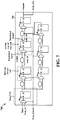
- FIG. 7 is a first diagram 700 illustrating a third exemplary apparatus and method associated with an asynchronous reset scheme for scan chains.
- the memory/core 720 includes a scan chain.
- the scan chain includes a plurality of scan cells coupled together.
- Each scan cell includes a multiplexer and a flip-flop.
- Scan cells that need to be reset to a first state s are configured (e.g., designed and manufactured/constructed) to be a first type of scan cell and scan cells that need to be reset to a second state s are configured (e.g., designed and manufactured/constructed) to be a second type of scan cell.
- the scan chain includes at least one of the first type of scan cell and at least one of the second type of scan cell.
- the first type of scan cell includes a multiplexer coupled to a non-reset/non-set flip-flop
- the second type of scan cell also includes a multiplexer coupled to a non-reset/non-set flip-flop.
- the second type of scan cell further includes a first inverter for inverting a scan_in signal input into the flip-flop, and a second inverter for inverting a scan_out signal output from the flip-flop.
- an apparatus includes at least one scan chain.
- Each of the at least one scan chain includes a plurality of scan cells coupled together.
- Each scan cell in the at least one scan chain includes a first type of scan cell when a reset state of the scan cell is a first state s , and a second type of scan cell different than the first type of scan cell when the reset state of the scan cell is a second state s .
- One or more scan chains of the at least one scan chain includes at least one of the first type of scan cell and at least one of the second type of scan cell.
- the first type of scan cell includes a multiplexer coupled to a flip-flop without both set and reset functionality.
- the second type of scan cell includes a multiplexer having a functional input and a scan input (scan_in).
- the second type of scan cell further includes a flip-flop without both set and reset functionality coupled to the multiplexer.
- the flip-flop has a functional output and a scan output (scan_out).
- the second type of scan cell further includes a first inverter coupled to the scan input, and a second inverter coupled to the scan output.
- the first state s is a 0 and the second state s is a 1.
- the first state s is a 1 and the second state s is a 0.
- FIG. 8 is a second diagram 800 illustrating the third exemplary apparatus and method associated with an asynchronous reset scheme for scan chains.
- a scan chain includes scan cells coupled together.
- the scan cells that need to be reset to the state s are configured to be a first type of scan cell and the scan cells that need to be reset to the state s are configured to be a second type of scan cell.
- Both the first and second types of scan cells include non-reset/non-set flip-flops.
- the second type of scan cells further include inverters so that the state s is input into the flip-flops 804 of the second type of scan cells and the state s is inverted to state s for output to subsequent scan cells.
- the state s is stored into each of the flip-flops 802 of the first type of scan cells, and the state s is stored into each of the flip-flops 804 of the second type of scan cells.
- all flip-flops are designed and manufactured to be non-reset/non-set flip-flops.
- the scan cells that need to be reset to the state s are designed and manufactured with non-reset/non-set flip-flops, and the scan cells that need to reset to the state s are designed and manufactured with non-reset/non-set flip-flops and inverters for inverting the scan input/output.
- use of the non-reset/non-set flip-flops in a scan chain requires a longer reset period for clocking a particular state through each of the flip-flops in the scan chain.
- the third exemplary apparatus and method reduces an area, power consumption, and speed of operation of the scan cells by utilizing non-reset/non-set flip-flops in all of the scan cells of a set of scan chains (which may or may not include all of the scan chains within the apparatus). Further, non-reset/non-set flip-flops are less susceptible than set/reset flip-flops during NTC operation.
- non-reset/non-set flip-flops Use of the non-reset/non-set flip-flops would therefore allow the use of a lower operating voltage during NTC operation than may be used when using reset/set flip-flops during NTC operation.
- use of non-reset/non-set flip-flops may save routing overhead for the reset/set pins.
- no reset control is required during a DFT when using non-reset/non-reset pins.
- FIG. 9 is a diagram 900 for illustrating first and third methods for performing an asynchronous reset in the first apparatus embodiment and third exemplary apparatus, respectively.
- the apparatus includes at least one scan chain and a reset controller/module.
- the reset controller/module inputs a first state into each of the at least one scan chain.
- Each of the at least one scan chain includes a plurality of scan cells coupled together.
- Each scan cell in the at least one scan chain is a first type of scan cell or a second type of scan cell.
- the at least one scan chain each includes at least one of the first type of scan cell and at least one of the second type of scan cell.
- step 904 the reset controller/module starts a clock to clock the first state through the first type of scan cells and the second type of scan cells until each flip-flop in the at least one scan chain stores one of the first state or a second state.
- step 906 the reset controller/module stops the clock. For this method, see also FIGs. 3 , 4 , 7 , and 8 .
- the first type of scan cell includes a multiplexer coupled to a first-type flip-flop without both set and reset functionality
- the second type of scan cell includes a multiplexer coupled to a second-type flip-flop with at least one of set or reset functionality.
- the clock is started to clock the first state through the scan cells until each flip-flop in the at least one scan chain stores the first state.
- the first state is a 0 and the second state is a 1
- the second-type flip-flop includes set functionality
- the reset controller/module sets, subsequent to stopping the clock, the second state into each of the second-type flip-flops within the at least one scan chain.
- the first state is a 1 and the second state is a 0,
- the second-type flip-flop includes reset functionality, and the reset controller/module resets, subsequent to stopping the clock, each of the second-type flip-flops within the at least one scan chain to store the second state.
- the clock is started to clock the first state through the scan cells until each of the first type of scan cell stores the first state and each of the second type of scan cell stores a second state different than the first state.
- the first type of scan cell includes a multiplexer coupled to a flip-flop without both set and reset functionality
- the second type of scan cell includes a multiplexer having a functional input and a scan input.
- the second type of scan cell further includes a flip-flop without both set and reset functionality coupled to the multiplexer.
- the flip-flop has a functional output and a scan output.
- the second type of scan cell further includes a first inverter coupled to the scan input for inverting the first state to the second state for input to the flip-flop.
- the second type of scan cell further includes a second inverter coupled to the scan output for inverting the second state to the first state on output from the flip-flop.
- the first state is a 0 and the second state is a 1.
- the first state is a 1 and the second state is a 0.
- an apparatus for performing an asynchronous reset includes at least one scan chain.
- the apparatus includes means for inputting a first state into each of the at least one scan chain.
- Each of the at least one scan chain includes a plurality of scan cells coupled together.
- Each scan cell in the at least one scan chain is a first type of scan cell or a second type of scan cell.
- the at least one scan chain each includes at least one of the first type of scan cell and at least one of the second type of scan cell.
- the apparatus further includes means for starting a clock to clock the first state through the first type of scan cells and the second type of scan cells until each flip-flop in the at least one scan chain stores one of the first state or a second state.
- the apparatus further includes means for stopping the clock.
- the first type of scan cell may include a multiplexer coupled to a first-type flip-flop without both set and reset functionality
- the second type of scan cell may include a multiplexer coupled to a second-type flip-flop with at least one of set or reset functionality.
- the means for starting the clock may clock the first state through the scan cells until each flip-flop in the at least one scan chain stores the first state.
- the first state is a 0 and the second state is a 1
- the second-type flip-flop includes set functionality
- the apparatus further includes means for setting, subsequent to stopping the clock, the second state into each of the second-type flip-flops within the at least one scan chain.
- the first state is a 1 and the second state is a 0, the second-type flip-flop includes reset functionality, and the apparatus further includes means for resetting, subsequent to stopping the clock, each of the second-type flip-flops within the at least one scan chain to store the second state.
- the means for starting the clock clocks the first state through the scan cells until each of the first type of scan cell stores the first state and each of the second type of scan cell stores a second state different than the first state.
- the first type of scan cell includes a multiplexer coupled to a flip-flop without both set and reset functionality
- the second type of scan cell includes a multiplexer having a functional input and a scan input and a flip-flop without both set and reset functionality coupled to the multiplexer.
- the flip-flop has a functional output and a scan output.
- the second type of scan cell further includes a first inverter coupled to the scan input for inverting the first state to the second state for input to the flip-flop, and a second inverter coupled to the scan output for inverting the second state to the first state on output from the flip-flop.
- the first state is a 0 and the second state is a 1.
- the first state is a 1 and the second state is a 0.
- FIG. 10 is a diagram 1000 for illustrating a second method for performing an asynchronous reset in the second exemplary apparatus.
- the apparatus includes a plurality of scan chains and a reset controller/module.
- the reset controller/module inputs a first state into each scan chain of a first set of scan chains of the plurality of scan chains.
- Each scan chain of the first set of scan chains includes a plurality of scan cells coupled together.
- Each scan cell in the first set of scan chains includes flip-flops without both set and reset functionality.
- the reset controller/module inputs a second state into each scan chain of a second set of scan chains of the plurality of scan chains.
- Each scan chain of the second set of scan chains includes a plurality of scan cells coupled together.
- Each scan cell in the second set of scan chains includes flip-flops without both set and reset functionality.
- the reset controller/module starts a clock to clock the first state through the first set of scan chains until each flip-flop in the first set of scan chains stores the first state, and to clock the second state through the second set of scan chains until each flip-flop in the second set of scan chains stores the second state.
- the reset controller/module stops the clock. For this method, see also FIGs. 5 and 6 .
- an apparatus for performing an asynchronous reset includes a plurality of scan chains.
- the apparatus further includes means for inputting a first state into each scan chain of a first set of scan chains of the plurality of scan chains.
- Each scan chain of the first set of scan chains includes a plurality of scan cells coupled together.
- Each scan cell in the first set of scan chains includes flip-flops without both set and reset functionality.
- the apparatus further includes means for inputting a second state into each scan chain of a second set of scan chains of the plurality of scan chains.
- Each scan chain of the second set of scan chains includes a plurality of scan cells coupled together.
- Each scan cell in the second set of scan chains includes flip-flops without both set and reset functionality.
- the apparatus further includes means for starting a clock to clock the first state through the first set of scan chains until each flip-flop in the first set of scan chains stores the first state, and to clock the second state through the second set of scan chains until each flip-flop in the second set of scan chains stores the second state.
- the apparatus further includes means for stopping the clock.
- First, second, and third apparatuses and methods associated with an asynchronous reset scheme for scan chains are provided supra.
- scan cells that need to be reset to a first state s are designed and manufactured to include non-set/non-reset flip-flops, and scan cells that need to be reset to a second state s are designed manufactured to include set/reset flip-flops.
- scan cells that need to be reset to a first state s are linked together within scan chains of a first set of scan chains, and scan cells that need to be reset to a second state s are linked together within scan chains of a second set of scan chains.
- scan cells that need to be reset to a first state s are designed and manufactured to include non-set/non-reset flip-flops
- scan cells that need to be reset to a second state s are designed and manufactured to include non-set/non-reset flip-flops and inverters for inverting a scan input and scan output.
- non-set/non-reset flip-flops rather than set/reset flip-flops within scan cells reduces an area, power consumption, and speed of operation of the scan cells during all phases of operation of the scan cells.
- use of non-set/non-reset flip-flops rather than set/reset flip-flops within scan cells provides additional advantages, as non-reset/non-set flip-flops are less susceptible than set/reset flip-flops during NTC operation (which would allow the use of a lower operating voltage during NTC operation than may be used when using reset/set flip-flops during NTC operation), use of non-reset/non-set flip-flops may save routing overhead for the reset/set pins, and no reset control is required during a DFT when using non-reset/non-reset pins.
- the second exemplary apparatus and method may provide the most advantages because scan cells that include set/reset flip-flops may all be replaced with scan cells that include non-set/non-reset flip-flops. However, the second exemplary apparatus and method may not be available if it is not possible to design scan cells with a first reset state to be linked together in one or more sets of scan chains, and scan cells with a second reset state to be linked together in one or more different sets of scan chains.
- the third exemplary apparatus and method provide the next best advantage because scan cells that include set/reset flip-flops may all be replaced with scan cells that include non-set/non-reset flip-flops or scan cells that include both non-set/non-reset flip-flops and inverters.
- the inverters are not in the functional path, and therefore do not slow operation during normal operation in a functional phase.
- the first exemplary apparatus and method also provide an advantage, as all of the set/reset flip-flops that are reset to a first state may be replaced with non-set/non-reset flip-flops.
- Combinations such as "at least one of A, B, or C,” “at least one of A, B, and C,” and “A, B, C, or any combination thereof' include any combination of A, B, and/or C, and may include multiples of A, multiples of B, or multiples of C.
- combinations such as “at least one of A, B, or C,” “at least one of A, B, and C,” and “A, B, C, or any combination thereof' may be A only, B only, C only, A and B, A and C, B and C, or A and B and C, where any such combinations may contain one or more member or members of A, B, or C.
Landscapes
- Engineering & Computer Science (AREA)
- General Engineering & Computer Science (AREA)
- Physics & Mathematics (AREA)
- General Physics & Mathematics (AREA)
- Tests Of Electronic Circuits (AREA)
- Semiconductor Integrated Circuits (AREA)
- Shift Register Type Memory (AREA)
- Electronic Switches (AREA)
Claims (2)
- Eine Vorrichtung (300), die wenigstens eine Scan-Kette bzw. Abtast-Kette (320) aufweist, wobei jede der wenigstens einen Scan-Kette (320) eine Vielzahl von Scan-Zellen aufweist, die miteinander gekoppelt sind, wobei jede Scan-Zelle in der wenigstens einen Scan-Kette Folgendes aufweist:einen ersten Typ einer Scan-Zelle, wobei ein Zurücksetzungs- bzw. Reset-Zustand der Scan-Zelle ein erster Zustand ist, wobei der erste Typ einer Scan-Zelle ein Flip-Flop (302, 304, 308, 312, 314) eines ersten Typs ohne eingebaute Set- und Reset-Schaltkreise bzw. Setz- und Zurücksetzungsschaltkreise aufweist; undeinen zweiten Typ einer Scan-Zelle, der sich von dem ersten Typ einer Scan-Zelle unterscheidet, wenn der Reset-Zustand der Scan-Zelle ein zweiter Zustand ist, wobei der zweite Typ einer Scan-Zelle ein Flip-Flop (306, 310) eines zweiten Typs mit eingebauten Setzschaltkreisen aufweist,wobei der erste Typ einer Scan-Zelle weiter einen Multiplexer aufweist, der an das Flip-Flop (302, 304, 308, 312, 314) des ersten Typs gekoppelt ist, und der zweite Typ einer Scan-Zelle weiter einen Multiplexer aufweist, der an ein Flip-Flop (306, 310) des zweiten Typs gekoppelt ist,wobei eine oder mehrere Scan-Ketten der wenigstens einen Scan-Kette wenigstens eine von einem ersten Typ einer Scan-Zelle und wenigstens eine von einem zweiten Typ einer Scan-Zelle aufweisen,wobei der erste Zustand eine 0 ist und der zweite Zustand eine 1 ist,wobei die Vorrichtung (300) weiter ein Zurücksetzungs- bzw. Reset-Modul (102) aufweist, das konfiguriert ist zum asynchronen Zurücksetzen der wenigstens einen Scan-Kette, wobei zum asynchronen Zurücksetzen der wenigstens einen Scan-Kette das Reset-Modul (102) konfiguriert ist zum:Eingeben des ersten Zustandes in jede von der wenigstens einen Scan-Kette;Starten eines Zeitgebers zum Takten des ersten Zustandes durch die Scan-Zelle, bis jedes Flip-Flop (302, 304, 306, 308, 310, 312, 314) in der wenigstens einen Scan-Kette den ersten Zustand speichert;Anhalten des Zeitgebers; undSetzen, nachfolgend auf das Anhalten des Zeitgebers, des zweiten Zustandes in jedes der Flip-Flops (306, 310) des zweiten Typs innerhalb der wenigstens einen Scan-Kette.
- Ein Verfahren (900) zum Durchführen eines asynchronen Reset bzw. einer asynchronen Zurücksetzung in einer Vorrichtung, die wenigstens eine Scan-Kette beinhaltet, wobei das Verfahren Folgendes aufweist:Eingeben (902) eines ersten Zustandes in jede der wenigstens einen Scan-Kette, wobei jede der wenigstens einen Scan-Kette eine Vielzahl von Scan-Zellen aufweist, die miteinander gekoppelt sind, wobei jede Scan-Zelle in der wenigstens einen Scan-Kette ein erster Typ einer Scan-Zelle oder ein zweiter Typ einer Scan-Zelle ist, wobei der erste Typ von Scan-Zelle ein Flip-Flop eines ersten Typs ohne eingebaute Set- und Reset-Schaltkreise bzw. Setz- und Zurücksetzungsschaltkreise aufweist, wobei der zweite Typ von Scan-Zelle ein Flip-Flop eines zweiten Typs mit eingebauten Set- bzw. Setzschaltkreisen aufweist, wobei die wenigstens eine Scan-Kette wenigstens eine des ersten Typs von Scan-Zelle und wenigstens eine des zweiten Typs von Scan-Zelle beinhaltet, wobei der erste Typ von Scan-Zelle weiter einen Multiplexer aufweist, der an das Flip-Flop des ersten Typs gekoppelt ist, und der zweite Typ von Scan-Zelle weiter einen Multiplexer aufweist, der an das Flip-Flop des zweiten Typs gekoppelt ist;Starten (904) eines Zeitgebers zum Takten des ersten Zustandes durch den ersten Typ von Scan-Zellen und den zweiten Typ von Scan-Zellen, bis jedes Flip-Flop in der wenigstens einen Scan-Kette den ersten Zustand speichert;
undAnhalten (906) des Zeitgebers,wobei der erste Zustand eine 0 ist und der zweite Zustand eine 1 ist, wobei das Flip-Flop des zweiten Typs die eingebauten Set- bzw. Setzschaltkreise beinhaltet, und das Verfahren weiter Folgendes aufweist Setzen (908), nachfolgend auf das Anhalten des Zeitgebers, des zweiten Zustandes in jedes der Flip-Flops des zweiten Typs innerhalb der wenigstens einen Scan-Kette.
Applications Claiming Priority (2)
| Application Number | Priority Date | Filing Date | Title |
|---|---|---|---|
| US14/251,297 US9564877B2 (en) | 2014-04-11 | 2014-04-11 | Reset scheme for scan chains with asynchronous reset signals |
| PCT/US2015/020036 WO2015156949A1 (en) | 2014-04-11 | 2015-03-11 | Reset scheme for scan chains with asynchronous reset signals |
Publications (2)
| Publication Number | Publication Date |
|---|---|
| EP3129798A1 EP3129798A1 (de) | 2017-02-15 |
| EP3129798B1 true EP3129798B1 (de) | 2020-03-11 |
Family
ID=52780036
Family Applications (1)
| Application Number | Title | Priority Date | Filing Date |
|---|---|---|---|
| EP15713279.6A Active EP3129798B1 (de) | 2014-04-11 | 2015-03-11 | Rücksetzungsschema für abtastketten mit asynchronen rücksetzungssignalen |
Country Status (7)
| Country | Link |
|---|---|
| US (1) | US9564877B2 (de) |
| EP (1) | EP3129798B1 (de) |
| JP (1) | JP6178022B2 (de) |
| KR (1) | KR20160145000A (de) |
| CN (1) | CN106164687B (de) |
| BR (1) | BR112016023739A2 (de) |
| WO (1) | WO2015156949A1 (de) |
Families Citing this family (8)
| Publication number | Priority date | Publication date | Assignee | Title |
|---|---|---|---|---|
| US9606182B2 (en) * | 2014-06-16 | 2017-03-28 | Samsung Electronics Co., Ltd. | System on chip |
| EP3367114A1 (de) * | 2017-02-24 | 2018-08-29 | Commsolid GmbH | Extended-jtag-controller und verfahren zur funktionsrückstellung mithilfe des extended-jtag-controllers |
| US10026498B1 (en) | 2017-04-10 | 2018-07-17 | International Business Machines Corporation | Simultaneous scan chain initialization with disparate latches |
| US10990319B2 (en) | 2018-06-18 | 2021-04-27 | Micron Technology, Inc. | Adaptive watchdog in a memory device |
| WO2020038570A1 (en) * | 2018-08-22 | 2020-02-27 | Commsolid Gmbh | Extended jtag controller and method for functional reset using the extended jtag controller |
| CN112684327B (zh) * | 2020-11-30 | 2023-09-05 | 海光信息技术股份有限公司 | 扫描链及其设计方法和基于扫描链的串行扫描复位方法 |
| US12088301B2 (en) * | 2022-03-16 | 2024-09-10 | Micron Technology, Inc. | Resetting integrated circuits |
| TWI865906B (zh) * | 2022-08-17 | 2024-12-11 | 立積電子股份有限公司 | 積體電路及其測試方法 |
Family Cites Families (22)
| Publication number | Priority date | Publication date | Assignee | Title |
|---|---|---|---|---|
| US5774477A (en) * | 1995-12-22 | 1998-06-30 | Lucent Technologies Inc. | Method and apparatus for pseudorandom boundary-scan testing |
| US5754455A (en) | 1996-04-10 | 1998-05-19 | Motorola, Inc. | Method and apparatus for setting a bit-serial filter to an all-zero state |
| US5793315A (en) | 1996-05-31 | 1998-08-11 | Motorola, Inc. | Bit-serial digital expandor |
| US5881067A (en) | 1997-01-28 | 1999-03-09 | Sun Microsystems, Inc. | Flip-flop design and technique for scan chain diagnosis |
| US6519724B1 (en) * | 1999-03-22 | 2003-02-11 | Koninklijke Philips Electronics N.V. | Communication systems, circuits, circuit systems and methods of operating a circuit |
| US6393592B1 (en) * | 1999-05-21 | 2002-05-21 | Adaptec, Inc. | Scan flop circuitry and methods for making the same |
| JP3851782B2 (ja) | 2001-03-07 | 2006-11-29 | 株式会社東芝 | 半導体集積回路及びそのテスト方法 |
| JP3531635B2 (ja) * | 2001-10-22 | 2004-05-31 | 松下電器産業株式会社 | 半導体集積回路装置 |
| JP2004170244A (ja) * | 2002-11-20 | 2004-06-17 | Matsushita Electric Ind Co Ltd | 組み込み自己検査回路 |
| US7032148B2 (en) * | 2003-07-07 | 2006-04-18 | Syntest Technologies, Inc. | Mask network design for scan-based integrated circuits |
| JP2007040921A (ja) * | 2005-08-05 | 2007-02-15 | Matsushita Electric Ind Co Ltd | スキャンチェーンにおける故障位置特定方法 |
| JP2007233842A (ja) | 2006-03-02 | 2007-09-13 | Matsushita Electric Ind Co Ltd | リセット動作検証回路の生成方法 |
| EP1939641B1 (de) | 2006-12-22 | 2009-06-10 | STMicroelectronics S.r.l. | Verbesserte Abtastkettenstruktur für erhöhte Diagnosekapazität von digitalen elektronischen Vorrichtungen |
| WO2008100520A2 (en) * | 2007-02-12 | 2008-08-21 | Mentor Graphics Corporation | Low power scan testing techniques and apparatus |
| JP2011247594A (ja) * | 2010-05-21 | 2011-12-08 | Renesas Electronics Corp | スキャンテスト装置及びスキャンテスト方法 |
| WO2012017269A1 (en) * | 2010-08-05 | 2012-02-09 | Freescale Semiconductor, Inc. | Electronic circuit and method for state retention power gating |
| CN102340304B (zh) | 2011-08-31 | 2013-05-01 | 北京时代民芯科技有限公司 | 一种tap接口优化电路 |
| CN102495356B (zh) | 2011-11-30 | 2014-11-05 | 福州大学 | 扫描链异步复位寄存器复位端口处理方法 |
| CN102495360B (zh) * | 2011-12-16 | 2014-05-07 | 浙江大学 | 一种安全扫描寄存器、安全扫描链及其扫描方法 |
| JP2014006109A (ja) * | 2012-06-22 | 2014-01-16 | Fujitsu Semiconductor Ltd | 故障診断回路、集積回路装置及び故障診断方法 |
| CN103023467B (zh) | 2012-11-28 | 2016-01-20 | 中国人民解放军国防科学技术大学 | 基于扫描方式的寄存器复位方法及装置 |
| CN102970013B (zh) | 2012-11-28 | 2015-03-25 | 中国人民解放军国防科学技术大学 | 基于扫描链的芯片内部寄存器复位方法及复位控制装置 |
-
2014
- 2014-04-11 US US14/251,297 patent/US9564877B2/en active Active
-
2015
- 2015-03-11 KR KR1020167028007A patent/KR20160145000A/ko not_active Withdrawn
- 2015-03-11 WO PCT/US2015/020036 patent/WO2015156949A1/en not_active Ceased
- 2015-03-11 BR BR112016023739A patent/BR112016023739A2/pt not_active IP Right Cessation
- 2015-03-11 CN CN201580018964.1A patent/CN106164687B/zh not_active Expired - Fee Related
- 2015-03-11 EP EP15713279.6A patent/EP3129798B1/de active Active
- 2015-03-11 JP JP2016561733A patent/JP6178022B2/ja not_active Expired - Fee Related
Non-Patent Citations (1)
| Title |
|---|
| None * |
Also Published As
| Publication number | Publication date |
|---|---|
| KR20160145000A (ko) | 2016-12-19 |
| CN106164687A (zh) | 2016-11-23 |
| BR112016023739A2 (pt) | 2017-08-15 |
| US20150295560A1 (en) | 2015-10-15 |
| EP3129798A1 (de) | 2017-02-15 |
| WO2015156949A1 (en) | 2015-10-15 |
| JP2017514222A (ja) | 2017-06-01 |
| CN106164687B (zh) | 2019-09-20 |
| JP6178022B2 (ja) | 2017-08-09 |
| US9564877B2 (en) | 2017-02-07 |
Similar Documents
| Publication | Publication Date | Title |
|---|---|---|
| US9564877B2 (en) | Reset scheme for scan chains with asynchronous reset signals | |
| US9772648B2 (en) | Low power asynchronous counters in a synchronous system | |
| EP3287799B1 (de) | Halbleiterbauelement und abtasttestverfahren | |
| US8717078B2 (en) | Sequential latching device with elements to increase hold times on the diagnostic data path | |
| US5870411A (en) | Method and system for testing self-timed circuitry | |
| KR101729004B1 (ko) | 상태 리텐션 회로 및 그 회로의 작동방법 | |
| KR20120005469A (ko) | 스캔 테스트를 지원하는 저전력 듀얼-에지-트리거 저장 셀 및 이를 위한 클럭 게이팅 회로 | |
| JP5058503B2 (ja) | スキャンテスト用回路を備える電子回路、集積回路及び該集積回路に用いられる消費電力低減方法 | |
| US7475309B2 (en) | Parallel test mode for multi-core processors | |
| US20140281651A1 (en) | Serial peripheral interface and methods of operating same | |
| US10658062B2 (en) | Simultaneous scan chain initialization with disparate latches | |
| US7026849B2 (en) | Reset circuit having synchronous and/or asynchronous modules | |
| US20130154707A1 (en) | Recoverable and reconfigurable pipeline structure for state-retention power gating | |
| US5912900A (en) | Method and system for testing self-timed circuitry | |
| CN119948467A (zh) | 用于外部双倍数据速率存储器接口的时钟限定器增强 | |
| US8890594B1 (en) | System for functional reset across multiple clock domains | |
| CN102402242A (zh) | 时钟管理单元 | |
| JP2004127012A (ja) | 同期式回路およびその設計方法 | |
| JP2011153917A (ja) | 半導体集積回路 |
Legal Events
| Date | Code | Title | Description |
|---|---|---|---|
| STAA | Information on the status of an ep patent application or granted ep patent |
Free format text: STATUS: THE INTERNATIONAL PUBLICATION HAS BEEN MADE |
|
| PUAI | Public reference made under article 153(3) epc to a published international application that has entered the european phase |
Free format text: ORIGINAL CODE: 0009012 |
|
| STAA | Information on the status of an ep patent application or granted ep patent |
Free format text: STATUS: REQUEST FOR EXAMINATION WAS MADE |
|
| 17P | Request for examination filed |
Effective date: 20160831 |
|
| AK | Designated contracting states |
Kind code of ref document: A1 Designated state(s): AL AT BE BG CH CY CZ DE DK EE ES FI FR GB GR HR HU IE IS IT LI LT LU LV MC MK MT NL NO PL PT RO RS SE SI SK SM TR |
|
| AX | Request for extension of the european patent |
Extension state: BA ME |
|
| DAV | Request for validation of the european patent (deleted) | ||
| DAX | Request for extension of the european patent (deleted) | ||
| REG | Reference to a national code |
Ref country code: DE Ref legal event code: R079 Ref document number: 602015048543 Country of ref document: DE Free format text: PREVIOUS MAIN CLASS: G01R0031318500 Ipc: G11C0019340000 |
|
| RIC1 | Information provided on ipc code assigned before grant |
Ipc: H03K 3/037 20060101ALI20190731BHEP Ipc: G11C 19/34 20060101AFI20190731BHEP Ipc: H03K 3/012 20060101ALI20190731BHEP Ipc: G01R 31/3185 20060101ALI20190731BHEP |
|
| GRAP | Despatch of communication of intention to grant a patent |
Free format text: ORIGINAL CODE: EPIDOSNIGR1 |
|
| STAA | Information on the status of an ep patent application or granted ep patent |
Free format text: STATUS: GRANT OF PATENT IS INTENDED |
|
| INTG | Intention to grant announced |
Effective date: 20191002 |
|
| RAP1 | Party data changed (applicant data changed or rights of an application transferred) |
Owner name: QUALCOMM INCORPORATED |
|
| GRAS | Grant fee paid |
Free format text: ORIGINAL CODE: EPIDOSNIGR3 |
|
| GRAA | (expected) grant |
Free format text: ORIGINAL CODE: 0009210 |
|
| STAA | Information on the status of an ep patent application or granted ep patent |
Free format text: STATUS: THE PATENT HAS BEEN GRANTED |
|
| AK | Designated contracting states |
Kind code of ref document: B1 Designated state(s): AL AT BE BG CH CY CZ DE DK EE ES FI FR GB GR HR HU IE IS IT LI LT LU LV MC MK MT NL NO PL PT RO RS SE SI SK SM TR |
|
| REG | Reference to a national code |
Ref country code: GB Ref legal event code: FG4D |
|
| REG | Reference to a national code |
Ref country code: CH Ref legal event code: EP |
|
| REG | Reference to a national code |
Ref country code: AT Ref legal event code: REF Ref document number: 1244126 Country of ref document: AT Kind code of ref document: T Effective date: 20200315 |
|
| REG | Reference to a national code |
Ref country code: DE Ref legal event code: R096 Ref document number: 602015048543 Country of ref document: DE |
|
| REG | Reference to a national code |
Ref country code: IE Ref legal event code: FG4D |
|
| PG25 | Lapsed in a contracting state [announced via postgrant information from national office to epo] |
Ref country code: FI Free format text: LAPSE BECAUSE OF FAILURE TO SUBMIT A TRANSLATION OF THE DESCRIPTION OR TO PAY THE FEE WITHIN THE PRESCRIBED TIME-LIMIT Effective date: 20200311 Ref country code: NO Free format text: LAPSE BECAUSE OF FAILURE TO SUBMIT A TRANSLATION OF THE DESCRIPTION OR TO PAY THE FEE WITHIN THE PRESCRIBED TIME-LIMIT Effective date: 20200611 Ref country code: RS Free format text: LAPSE BECAUSE OF FAILURE TO SUBMIT A TRANSLATION OF THE DESCRIPTION OR TO PAY THE FEE WITHIN THE PRESCRIBED TIME-LIMIT Effective date: 20200311 |
|
| REG | Reference to a national code |
Ref country code: NL Ref legal event code: MP Effective date: 20200311 |
|
| PG25 | Lapsed in a contracting state [announced via postgrant information from national office to epo] |
Ref country code: BG Free format text: LAPSE BECAUSE OF FAILURE TO SUBMIT A TRANSLATION OF THE DESCRIPTION OR TO PAY THE FEE WITHIN THE PRESCRIBED TIME-LIMIT Effective date: 20200611 Ref country code: HR Free format text: LAPSE BECAUSE OF FAILURE TO SUBMIT A TRANSLATION OF THE DESCRIPTION OR TO PAY THE FEE WITHIN THE PRESCRIBED TIME-LIMIT Effective date: 20200311 Ref country code: GR Free format text: LAPSE BECAUSE OF FAILURE TO SUBMIT A TRANSLATION OF THE DESCRIPTION OR TO PAY THE FEE WITHIN THE PRESCRIBED TIME-LIMIT Effective date: 20200612 Ref country code: SE Free format text: LAPSE BECAUSE OF FAILURE TO SUBMIT A TRANSLATION OF THE DESCRIPTION OR TO PAY THE FEE WITHIN THE PRESCRIBED TIME-LIMIT Effective date: 20200311 Ref country code: LV Free format text: LAPSE BECAUSE OF FAILURE TO SUBMIT A TRANSLATION OF THE DESCRIPTION OR TO PAY THE FEE WITHIN THE PRESCRIBED TIME-LIMIT Effective date: 20200311 |
|
| REG | Reference to a national code |
Ref country code: LT Ref legal event code: MG4D |
|
| PG25 | Lapsed in a contracting state [announced via postgrant information from national office to epo] |
Ref country code: NL Free format text: LAPSE BECAUSE OF FAILURE TO SUBMIT A TRANSLATION OF THE DESCRIPTION OR TO PAY THE FEE WITHIN THE PRESCRIBED TIME-LIMIT Effective date: 20200311 |
|
| PG25 | Lapsed in a contracting state [announced via postgrant information from national office to epo] |
Ref country code: LT Free format text: LAPSE BECAUSE OF FAILURE TO SUBMIT A TRANSLATION OF THE DESCRIPTION OR TO PAY THE FEE WITHIN THE PRESCRIBED TIME-LIMIT Effective date: 20200311 Ref country code: RO Free format text: LAPSE BECAUSE OF FAILURE TO SUBMIT A TRANSLATION OF THE DESCRIPTION OR TO PAY THE FEE WITHIN THE PRESCRIBED TIME-LIMIT Effective date: 20200311 Ref country code: SK Free format text: LAPSE BECAUSE OF FAILURE TO SUBMIT A TRANSLATION OF THE DESCRIPTION OR TO PAY THE FEE WITHIN THE PRESCRIBED TIME-LIMIT Effective date: 20200311 Ref country code: CZ Free format text: LAPSE BECAUSE OF FAILURE TO SUBMIT A TRANSLATION OF THE DESCRIPTION OR TO PAY THE FEE WITHIN THE PRESCRIBED TIME-LIMIT Effective date: 20200311 Ref country code: IS Free format text: LAPSE BECAUSE OF FAILURE TO SUBMIT A TRANSLATION OF THE DESCRIPTION OR TO PAY THE FEE WITHIN THE PRESCRIBED TIME-LIMIT Effective date: 20200711 Ref country code: PT Free format text: LAPSE BECAUSE OF FAILURE TO SUBMIT A TRANSLATION OF THE DESCRIPTION OR TO PAY THE FEE WITHIN THE PRESCRIBED TIME-LIMIT Effective date: 20200805 Ref country code: EE Free format text: LAPSE BECAUSE OF FAILURE TO SUBMIT A TRANSLATION OF THE DESCRIPTION OR TO PAY THE FEE WITHIN THE PRESCRIBED TIME-LIMIT Effective date: 20200311 Ref country code: SM Free format text: LAPSE BECAUSE OF FAILURE TO SUBMIT A TRANSLATION OF THE DESCRIPTION OR TO PAY THE FEE WITHIN THE PRESCRIBED TIME-LIMIT Effective date: 20200311 |
|
| REG | Reference to a national code |
Ref country code: CH Ref legal event code: PL |
|
| REG | Reference to a national code |
Ref country code: AT Ref legal event code: MK05 Ref document number: 1244126 Country of ref document: AT Kind code of ref document: T Effective date: 20200311 |
|
| REG | Reference to a national code |
Ref country code: DE Ref legal event code: R097 Ref document number: 602015048543 Country of ref document: DE |
|
| REG | Reference to a national code |
Ref country code: BE Ref legal event code: MM Effective date: 20200331 |
|
| PG25 | Lapsed in a contracting state [announced via postgrant information from national office to epo] |
Ref country code: MC Free format text: LAPSE BECAUSE OF FAILURE TO SUBMIT A TRANSLATION OF THE DESCRIPTION OR TO PAY THE FEE WITHIN THE PRESCRIBED TIME-LIMIT Effective date: 20200311 Ref country code: LU Free format text: LAPSE BECAUSE OF NON-PAYMENT OF DUE FEES Effective date: 20200311 |
|
| PLBE | No opposition filed within time limit |
Free format text: ORIGINAL CODE: 0009261 |
|
| STAA | Information on the status of an ep patent application or granted ep patent |
Free format text: STATUS: NO OPPOSITION FILED WITHIN TIME LIMIT |
|
| PG25 | Lapsed in a contracting state [announced via postgrant information from national office to epo] |
Ref country code: LI Free format text: LAPSE BECAUSE OF NON-PAYMENT OF DUE FEES Effective date: 20200331 Ref country code: CH Free format text: LAPSE BECAUSE OF NON-PAYMENT OF DUE FEES Effective date: 20200331 Ref country code: AT Free format text: LAPSE BECAUSE OF FAILURE TO SUBMIT A TRANSLATION OF THE DESCRIPTION OR TO PAY THE FEE WITHIN THE PRESCRIBED TIME-LIMIT Effective date: 20200311 Ref country code: ES Free format text: LAPSE BECAUSE OF FAILURE TO SUBMIT A TRANSLATION OF THE DESCRIPTION OR TO PAY THE FEE WITHIN THE PRESCRIBED TIME-LIMIT Effective date: 20200311 Ref country code: DK Free format text: LAPSE BECAUSE OF FAILURE TO SUBMIT A TRANSLATION OF THE DESCRIPTION OR TO PAY THE FEE WITHIN THE PRESCRIBED TIME-LIMIT Effective date: 20200311 Ref country code: IT Free format text: LAPSE BECAUSE OF FAILURE TO SUBMIT A TRANSLATION OF THE DESCRIPTION OR TO PAY THE FEE WITHIN THE PRESCRIBED TIME-LIMIT Effective date: 20200311 Ref country code: IE Free format text: LAPSE BECAUSE OF NON-PAYMENT OF DUE FEES Effective date: 20200311 |
|
| 26N | No opposition filed |
Effective date: 20201214 |
|
| PG25 | Lapsed in a contracting state [announced via postgrant information from national office to epo] |
Ref country code: BE Free format text: LAPSE BECAUSE OF NON-PAYMENT OF DUE FEES Effective date: 20200331 Ref country code: SI Free format text: LAPSE BECAUSE OF FAILURE TO SUBMIT A TRANSLATION OF THE DESCRIPTION OR TO PAY THE FEE WITHIN THE PRESCRIBED TIME-LIMIT Effective date: 20200311 Ref country code: PL Free format text: LAPSE BECAUSE OF FAILURE TO SUBMIT A TRANSLATION OF THE DESCRIPTION OR TO PAY THE FEE WITHIN THE PRESCRIBED TIME-LIMIT Effective date: 20200311 |
|
| PGFP | Annual fee paid to national office [announced via postgrant information from national office to epo] |
Ref country code: FR Payment date: 20210218 Year of fee payment: 7 |
|
| PGFP | Annual fee paid to national office [announced via postgrant information from national office to epo] |
Ref country code: DE Payment date: 20210210 Year of fee payment: 7 Ref country code: GB Payment date: 20210311 Year of fee payment: 7 |
|
| PG25 | Lapsed in a contracting state [announced via postgrant information from national office to epo] |
Ref country code: TR Free format text: LAPSE BECAUSE OF FAILURE TO SUBMIT A TRANSLATION OF THE DESCRIPTION OR TO PAY THE FEE WITHIN THE PRESCRIBED TIME-LIMIT Effective date: 20200311 Ref country code: MT Free format text: LAPSE BECAUSE OF FAILURE TO SUBMIT A TRANSLATION OF THE DESCRIPTION OR TO PAY THE FEE WITHIN THE PRESCRIBED TIME-LIMIT Effective date: 20200311 Ref country code: CY Free format text: LAPSE BECAUSE OF FAILURE TO SUBMIT A TRANSLATION OF THE DESCRIPTION OR TO PAY THE FEE WITHIN THE PRESCRIBED TIME-LIMIT Effective date: 20200311 |
|
| PG25 | Lapsed in a contracting state [announced via postgrant information from national office to epo] |
Ref country code: MK Free format text: LAPSE BECAUSE OF FAILURE TO SUBMIT A TRANSLATION OF THE DESCRIPTION OR TO PAY THE FEE WITHIN THE PRESCRIBED TIME-LIMIT Effective date: 20200311 Ref country code: AL Free format text: LAPSE BECAUSE OF FAILURE TO SUBMIT A TRANSLATION OF THE DESCRIPTION OR TO PAY THE FEE WITHIN THE PRESCRIBED TIME-LIMIT Effective date: 20200311 |
|
| REG | Reference to a national code |
Ref country code: DE Ref legal event code: R119 Ref document number: 602015048543 Country of ref document: DE |
|
| GBPC | Gb: european patent ceased through non-payment of renewal fee |
Effective date: 20220311 |
|
| PG25 | Lapsed in a contracting state [announced via postgrant information from national office to epo] |
Ref country code: GB Free format text: LAPSE BECAUSE OF NON-PAYMENT OF DUE FEES Effective date: 20220311 Ref country code: FR Free format text: LAPSE BECAUSE OF NON-PAYMENT OF DUE FEES Effective date: 20220331 Ref country code: DE Free format text: LAPSE BECAUSE OF NON-PAYMENT OF DUE FEES Effective date: 20221001 |