EP1939641B1 - Verbesserte Abtastkettenstruktur für erhöhte Diagnosekapazität von digitalen elektronischen Vorrichtungen - Google Patents
Verbesserte Abtastkettenstruktur für erhöhte Diagnosekapazität von digitalen elektronischen Vorrichtungen Download PDFInfo
- Publication number
- EP1939641B1 EP1939641B1 EP06026788A EP06026788A EP1939641B1 EP 1939641 B1 EP1939641 B1 EP 1939641B1 EP 06026788 A EP06026788 A EP 06026788A EP 06026788 A EP06026788 A EP 06026788A EP 1939641 B1 EP1939641 B1 EP 1939641B1
- Authority
- EP
- European Patent Office
- Prior art keywords
- flip
- scan chain
- output
- soctrl
- inverted
- Prior art date
- Legal status (The legal status is an assumption and is not a legal conclusion. Google has not performed a legal analysis and makes no representation as to the accuracy of the status listed.)
- Not-in-force
Links
- 238000012360 testing method Methods 0.000 claims description 17
- 230000000295 complement effect Effects 0.000 claims description 5
- 238000002955 isolation Methods 0.000 description 8
- 238000013461 design Methods 0.000 description 6
- 238000003745 diagnosis Methods 0.000 description 4
- 238000003780 insertion Methods 0.000 description 4
- 230000037431 insertion Effects 0.000 description 4
- 238000012986 modification Methods 0.000 description 4
- 230000004048 modification Effects 0.000 description 4
- 238000001514 detection method Methods 0.000 description 3
- 238000000034 method Methods 0.000 description 3
- 230000003111 delayed effect Effects 0.000 description 2
- XUIMIQQOPSSXEZ-UHFFFAOYSA-N Silicon Chemical group [Si] XUIMIQQOPSSXEZ-UHFFFAOYSA-N 0.000 description 1
- 238000013459 approach Methods 0.000 description 1
- 238000010420 art technique Methods 0.000 description 1
- 230000005540 biological transmission Effects 0.000 description 1
- 230000007547 defect Effects 0.000 description 1
- 230000009977 dual effect Effects 0.000 description 1
- 238000013507 mapping Methods 0.000 description 1
Images



Classifications
-
- G—PHYSICS
- G01—MEASURING; TESTING
- G01R—MEASURING ELECTRIC VARIABLES; MEASURING MAGNETIC VARIABLES
- G01R31/00—Arrangements for testing electric properties; Arrangements for locating electric faults; Arrangements for electrical testing characterised by what is being tested not provided for elsewhere
- G01R31/28—Testing of electronic circuits, e.g. by signal tracer
- G01R31/317—Testing of digital circuits
- G01R31/3181—Functional testing
- G01R31/3185—Reconfiguring for testing, e.g. LSSD, partitioning
- G01R31/318533—Reconfiguring for testing, e.g. LSSD, partitioning using scanning techniques, e.g. LSSD, Boundary Scan, JTAG
- G01R31/318541—Scan latches or cell details
Definitions
- the present invention relates in its more general aspect to an improved scan chain architecture, belonging to the field of Design For Testability techniques, to be used on digital devices in order to increase the diagnostic capability of fault categories which prevent the device scan chain to shift.
- the invention relates to a scan chain architecture for increased diagnostic capability in digital electronic devices, said scan chain including a cascade of flip-flop cells each having at least one> input and at least one output or an inverted output and wherein the output or the inverted output of a flip-flop of the chain is connected to the input of the subsequent flip-flop in the scan chain.
- the invention also relates to a dedicated logic circuitry added to a basic flip-flop cell of a scan chain for further improving the detection and isolation of possible fault categories.
- the invention particularly, but not exclusively, allows identifying a list of fault categories whose detection and isolation can be made possible, and the following description is made with reference to this list for convenience of explanation only.
- the currently available scan chain structures are built stitching the device flip-flops in order to satisfy different constraints such as: minimization of routing (physical scan insertion), minimization of hold time problem, by hierarchical name, and so on.
- the typical connections between two consecutive flip-flops 1 of a scan chain 9 are performed considering one or a combination of the above constraints. Provided that all flip-flops have both a normal output, identified as Q, and an inverted output, reported in Figure 1 as QN, in some cases Q happens to be connected to the flip-flop input TI of the next flip-flop of the scan chain, while in the other cases the connection is between QN and TI. In other word, the outputs Q or QN of a given flip-flop are linked to the input of the subsequent flip-flop not according to a specific rule but rather according to the specific requirement or requirements of the specific scan chain.
- the US patent application No. 5 313 470 in the name of Simpson at al., relates to a scan circuit for clock inputs which, during a switch from (or to) a test mode, avoids a transmission of undesired impulse.
- the US patent application No. 5 488 318 in the name of Vajapey et al., relates to a multifunction register with exclusive NOR, for combining the output of a plurality of scan registers.
- the technical problem underlying the present invention is that of providing an improved connection configuration having characteristics allowing to perform the diagnosis of possible failures whilst requiring the knowledge of the scan chain structure only, thus overcoming the limits which still affect the devices realised according to the prior art, and introducing only a small, and often null, area overhead into the HW structure.
- the solution idea underlying the present invention is that of modifying the scan chain structure of known type by using a dedicated logic circuitry to connect consecutive flip-flops belonging to a same scan chain. In this manner it is possible improving the diagnostic capability by means of a more efficient use of the asynchronous initialization of the scan chain flip-flops.
- the status of the scan chain flip-flops must be initialized using an asynchronous pin (set or reset), which is typically present in all the flip-flops adopted in digital design and connected to the external reset or set when scan mode is enabled.
- the invention relates to a modification of the logic circuitry connecting consecutive flip-flops of the same scan chain, in order to achieve the diagnostic capability improvement which allows the identification of predetermined fault categories preventing the scan chain to properly shift. Since all the flip-flops adopted in digital designs are typically asynchronously initialized using a dedicated set or reset pin, the above proposed solutions quite cover the whole world of digital devices.
- an improved scan chain architecture including dedicated logic circuitry connecting consecutive flip-flops of the same scan chain as defined by the characterising part of claim 1 and following.
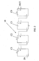
- the architecture 10 may be structured with a scan chain of flip-flop cells of known type, for instance those indicated with 2 in figure 1 , that are linked one to the other according to the rules provided by the present invention and disclosed hereinafter.
- the architecture 10 may be structured with a scan chain of flip-flop cells 5 that have been modified with respect to known flip flop cells 3, as shown in Figures 3 and 4
- a low cost / capability solution will be disclosed first and a high cost / capability solution will be disclosed later.
- the two solutions are based on a different ways of connecting toghether consecutive flip-flops cells in the same scan chain.
- the low cost / capability solution presents advantages in term of area overhead while the high cost / capability solution presents advantages in terms of performances.
- the difference between the Q, QN and SO, SON resides in their functional scope.
- the output Q, QN are functional outputs and fast signals while SO, SON are slower signals that are provided in the flip flop cells to be dedicated to the scan routing of the scan chain.
- the logic values of the output Q generally corresponds to the logic value of the output SO and this is also true for the other outputs QN, SON. If the logic values of the output Q should not correspond to the logic value of the output SO, only the pins SO/SON could be used.
- the key point that allows to improve the diagnostic capability with respect to a failure of the scan chain shifting is to have, at every shift clock cycle, a toggling on the flip-flop output to identify and point out the element or event that broke the scan shifting.
- the only requirement is to execute a post analysis of the scan structure, i.e. after the scan insertion is performed, in order to slightly modify the scan chain architecture.
- the invention teaches to modify the connection between these two flip-flops C0, C1 in order to have an inversion among them.
- the flip-flops should have both the output Q and QN; as an alternative these flip-flop cells C0, C1 might have a dedicated output of the kind SCAN OUT, that is identified with SO in the figure 3 , and is delayed to prevent hold problem during the physical stitching. In this specific case using the output SO even an inverted output SON should be present.
- INV x , x - 1 NOT ⁇ S x ⁇ XOR S x - 1 ⁇ XOR S x - conn - S x - 1
- INV x,x-1 is a logic function that has to be used for modifying the connection.
- the output of a good shift-out after the external reset/set has been applied, will be a sequence of toggling at every shift clock cycles.
- the invention suggests a modification in the connections between two consecutive flip-flops C0, C1,...Cx, Cx+1..., Cn-1; Cn of the scan chain in order to achieve an inversion of the input TI of the C x-th flip-flop of the scan chain, depending on the status of the same flip flop C x-th and on the status of the previous C (x+1)th flip-flop. Moreover, even the status of the connection between those flip-flops is taken in consideration.
- the flip-flops of the scan chain are here supposed to be numbered increasingly from the flip-flop cell C0 closer to the scan chain output (OUT) to the one Cn closer to the scan chain input (IN).
- S x , S x-1 , and S x -conn-S x-1 indicate the status of the two consecutive flip-flops after asynchronous set or reset initialization and of the logic relation of the original connection between them, respectively.
- the term (S x -conn-S x-1 ) is considered 1 in case of an inversion and 0 in case of a buffer (no inversion). This is substantially the low cost solution shown in figure 2 .
- the output sequence matches the expected value at some clock cycles, while being inverted at others, depending on the number of single Hold problem in the scan chain.
- the reason for the impossibility to completely isolate the problem is related to the fact that the status of the scan chain elements, S x and S x+1 , have a fixed relation between them, so that a couple of faults on S x and S x+1 cannot be distinguished.
- the value of the fault depends on the location where the fault is detected and the set/reset asynchronous signal used to initialize the related flip-flops.
- the solution proposed by the present invention may be considered a middle cost solution .
- the high Cost / Capability solution is basically similar to the previously disclosed low cost solution but, in order to improve the diagnostic capability of the previous solution in the cases where the detection or the isolation is not possible, some modifications to the scan chain structure and cells are performed.
- flip-flops 5 having two separate outputs: one for the functional behavior Q and one for the scan chain stitching SO.
- the simpler and smaller proposal for the implementation of the high cost / capability solution is to modify the basic flip-flop cells 3, introducing a control signal SOCtrl and a further controlled output SO_SON.
- the cell 5 includes the cell 3 and a dedicated logic circuitry 6, for instance a simple multiplexer circuit 6 enabled by the signal SOCtrl.
- This multiplexer 6 has a couple of inputs: A, that is equivalent to SO, and B, that is equivalent to the inverted value of SO (indicated as SON).
- the basic idea is that of having three different configurations: one behaves exactly like the previous one (i.e. one toggling for every flip-flop), the second approach generates or not an inversion depending on the flip-flop position in the scan chain (odd flip-flops have inversion, while even ones don't have the inversion, i.e. one toggle every two flip-flops), and a third configuration that is a complementary configuration with respect to the second one (i.e. even ones have inversion, while odd ones don't).
- the signals SOCtrl_ODD and INV_SOCtrl_ODD must be used for the Flip-Flop cells being in odd position (C1,C3,%) while the signals SOCtrl_EVEN and INV _SOCtr1_EVEN must be used for the even positions (C0,C2,).
- Each Flip-Flop cell must be connected to the respective inverted (INV_SOCtr1...) connection or non inverted (SOCtr_1...) connection according to the rule reported in the equation 1; if an inverted connection is required (INV x,x-1 , IS EQUAL TO 1) a connection to INV_SOCtrl_(ODD/EVEN) is established otherwise to the other signal SOCtr1_(ODD/EVEN).
- the first test to be-performed is in line with the previous description and must keep the same functionality of the low cost / capability solution test.
- a second test can be performed by forcing the potential value of the signal SOCtrl_ODD to VDD (thus INV_SOCTRL_ODD to GND) and the SOCtrl_EVEN to GND. This operation is enough to isolate double consecutive Hold Time, because there is always an inversion between two consecutive flip-flops that allows the isolation of the problem.
- a third possible test is complementary to the second one, so SOCtrl_EVEN will be forced to VDD, while SOCtrl_ODD is forced to GND.
- This testing mode will confirm the failure location of the second test.
- an enable pin TE not shown in the drawings, is normally used to enable between the input pin TI, starting the scan mode, and another input pin D, starting the user mode.
- the testing mode of the present invention allows the isolation of the stuck - at 0 on TE closer to scan out, because applying these two tests the User Data will be the same (the reset state of the device flip-flops doesn't change) but the TI input will be complementary depending on the previous SOCtrl status.
- this structure allows the diagnosis and isolation of several typologies of Hold problems (also multiple), which can really be one of the main problem for the sub-micron technology.
- the only limitation to this structure is the case of Multiple Stuck - at in the same scan chain: in this case the diagnostic capability is the same as the low cost / capability solution.
- control signals reported in figure 4 may be provided by external pads or by a dedicated test logic portion.
Landscapes
- Engineering & Computer Science (AREA)
- General Engineering & Computer Science (AREA)
- Physics & Mathematics (AREA)
- General Physics & Mathematics (AREA)
- Tests Of Electronic Circuits (AREA)
- Test And Diagnosis Of Digital Computers (AREA)
Claims (12)
- Verbesserte Scan-Ketten-Architektur für erhöhte Diagnosefähigkeit in digitalen elektronischen Vorrichtungen, wobei die Scan-Kette eine Kaskade von Flip-Flop-Zellen (C0, C1 ..., Cx-1; Cx, ..., Cn) aufweist, von denen jede mindestens einen Eingang (T1, S-IN) und mindestens einen Ausgang (Q) oder einen invertierten Ausgang (QN) hat, und wobei der Ausgang (Q) oder der invertierte Ausgang (QN) eines Flip-Flops der Kette mit dem Eingang des darauf folgenden Flip-Flops in der Scan-Kette verbunden ist, dadurch gekennzeichnet, dass sie eine zugeordnete Logikschaltungsanordnung (6) zum Auswählen einer Verbindung zwischen zwei aufeinander folgenden Flip-Flops (Cx, Cx-1) der Scan-Kette (10) entsprechend dem Status einer gegebenen Flip-Flop-Zelle aufweist, wobei der Status der vorhergehenden Flip-Flop-Zelle und der Status der Verbindung zwischen ihnen der folgenden Beziehung entspricht:

wobei Sx, Sx-1 und (Sx-conn-Sx-1) den Status der beiden aufeinander folgenden Flip-Flop-Zellen (Cx, Cx-1) nach einer Initialisierung (set, reset) und den Status einer Originalverbindung zwischen ihnen anzeigen, vorausgesetzt, dass die Verbindung zwischen den beiden aufeinander folgenden Flip-Flops (Cx, Cx-1) im Bezug auf die Originalverbindung invertiert ist, wenn INVx,x-1 = 1. - Verbesserte Scan-Ketten-Architektur nach Anspruch 1, wobei die Flip-Flop-Zellen einen alternativen Ausgang (SO) vom SCAN OUT-Typ aufweisen und als alternativer invertierter Ausgang (SON) ein Komplementärsignal des alternativen Ausgangs (SO) verwendet wird und diese weiteren Ausgänge (SO, SON) zum Verbinden von aufeinander folgenden Flip-Flop-Zellen (Cx, Cx-1) gemäß oben genannter Beziehung und alternativ zu dem Ausgang (Q) oder dem invertierten Ausgang (QN) der Flip-Flop-Zellen verwendet werden können.
- Verbesserte Scan-Ketten-Architektur nach Anspruch 1, wobei zwischen dem Ausgang (Q) und dem Eingang (TI) zweier aufeinander folgender Flip-Flops ein Inverter eingefügt wird, wenn der invertierte Ausgang (ON) nicht in der Flip-Flop-Bibliothek verfügbar ist und eine Verbindung über den invertierten Ausgang (QN) erforderlich ist.
- Verbesserte Scan-Ketten-Architektur nach Anspruch 2, wobei zwischen dem alternativen Ausgang (SO) und dem Eingang (TI) zweier aufeinander folgender Flip-Flops ein Inverter eingefügt wird, wenn der alternative invertierte Ausgang (SON) nicht in der Flip-Flop-Bibliothek verfügbar ist und eine Verbindung über den alternativen invertierten Ausgang (SON) erforderlich ist.
- Verbesserte Scan-Ketten-Architektur nach Anspruch 2, gekennzeichnet durch die Tatsache, dass die Flip-Flop-Zellen ein Steuersignal (SOCtrl) empfangen und die zugeordnete Logikschaltungsanordnung (6) eine weitere gesteuerte Ausgabe (SO_SON) gemäß einem Logikzustandswert des Steuersignals (SOCtrl) liefert.
- Verbesserte Scan-Ketten-Architektur nach Anspruch 5, dadurch gekennzeichnet, dass die zugeordnete Logikschaltungsanordnung (6) einen Multiplexer aufweist, der als Eingaben das Signal des alternativen Ausgangs (SO) und das Komplementärsignal des alternativen Ausgangs (SO) empfängt und die weitere gesteuerte Ausgabe (SO_SON) gemäß dem Logikzustandswert des Steuersignals (SOCtrl) liefert.
- Verbesserte Scan-Ketten-Architektur nach Anspruch 6, dadurch gekennzeichnet, dass die weitere gesteuerte Ausgabe (SO_SON) gemäß dem Logikzustandswert des Steuersignals (SOCtrl) von dem alternativen Ausgang umgeschaltet wird.
- Verbesserte Scan-Ketten-Architektur nach Anspruch 6, dadurch gekennzeichnet, dass die Flip-Flop-Zellen, die den Multiplexer aufweisen, Zellen mit asynchroner Rücksetzung oder Einstellung sind.
- Verbesserte Scan-Ketten-Architektur nach Anspruch 6, dadurch gekennzeichnet, dass zwei verschiedene Steuersignale (SOCtrl_ODD; SOCtrl-EVEN) zum Treiben der Zellen mit ungeraden Positionen (C1, C3 ...) bzw. der Zellen mit geraden Positionen (C0, C2 ...) der Kette geliefert werden.
- Verbesserte Scan-Ketten-Architektur nach Anspruch 9, dadurch gekennzeichnet, dass auch entsprechende invertierte Steuersignale (INV_SOCtrl_ODD; INV _SOCtrl_EVEN) geliefert werden, wobei jede Flip-Flop-Zelle mit der jeweiligen invertierten (INV_SOCtrl_ ...) Verbindung oder nicht invertierten (SOCtrl_ ...) Verbindung verbunden ist gemäß der in der Beziehung aufgezeigten Regel; wenn eine invertierte Verbindung erforderlich ist (INVx,x-1 ist gleich 1), wird eine Verbindung zu INV_SOCtrl_(ODD/EVEN), andernfalls zu dem anderen Signal SOCtrl_ (ODD/EVEN) hergestellt.
- Verbesserte Scan-Ketten-Architektur nach Anspruch 10, dadurch gekennzeichnet, dass die Steuersignale (SOCtrl_ODD; SOCtrl_EVEN) und die invertierten Steuersignale (INV_SOCtrl_ODD; INV_SOCtrl_EVEN) von externen Pads oder von einem zugeordneten Testlogikteil geliefert werden.
- Verbesserte Scan-Ketten-Architektur nach Anspruch 6, dadurch gekennzeichnet, dass eine zugeordnete Bibliothek verwendet wird, in der es für jedes Original-Flip-Flop-Element ein modifiziertes Flip-Flop (5) mit einer anderen Polarität des Steuersignals (SOCtrl) gibt, um in dem Fall verwendet zu werden, wenn ein invertierter Steuersignalwert statt einer invertierten Steuerleitung (INV _SOCtrl_ODD /EVEN) erforderlich ist.
Priority Applications (3)
| Application Number | Priority Date | Filing Date | Title |
|---|---|---|---|
| EP06026788A EP1939641B1 (de) | 2006-12-22 | 2006-12-22 | Verbesserte Abtastkettenstruktur für erhöhte Diagnosekapazität von digitalen elektronischen Vorrichtungen |
| DE602006007241T DE602006007241D1 (de) | 2006-12-22 | 2006-12-22 | Verbesserte Abtastkettenstruktur für erhöhte Diagnosekapazität von digitalen elektronischen Vorrichtungen |
| US11/963,036 US7900103B2 (en) | 2006-12-22 | 2007-12-21 | Scan chain architecture for increased diagnostic capability in digital electronic devices |
Applications Claiming Priority (1)
| Application Number | Priority Date | Filing Date | Title |
|---|---|---|---|
| EP06026788A EP1939641B1 (de) | 2006-12-22 | 2006-12-22 | Verbesserte Abtastkettenstruktur für erhöhte Diagnosekapazität von digitalen elektronischen Vorrichtungen |
Publications (2)
| Publication Number | Publication Date |
|---|---|
| EP1939641A1 EP1939641A1 (de) | 2008-07-02 |
| EP1939641B1 true EP1939641B1 (de) | 2009-06-10 |
Family
ID=38117012
Family Applications (1)
| Application Number | Title | Priority Date | Filing Date |
|---|---|---|---|
| EP06026788A Not-in-force EP1939641B1 (de) | 2006-12-22 | 2006-12-22 | Verbesserte Abtastkettenstruktur für erhöhte Diagnosekapazität von digitalen elektronischen Vorrichtungen |
Country Status (3)
| Country | Link |
|---|---|
| US (1) | US7900103B2 (de) |
| EP (1) | EP1939641B1 (de) |
| DE (1) | DE602006007241D1 (de) |
Families Citing this family (5)
| Publication number | Priority date | Publication date | Assignee | Title |
|---|---|---|---|---|
| US9564877B2 (en) * | 2014-04-11 | 2017-02-07 | Qualcomm Incorporated | Reset scheme for scan chains with asynchronous reset signals |
| US9274171B1 (en) | 2014-11-12 | 2016-03-01 | International Business Machines Corporation | Customer-transparent logic redundancy for improved yield |
| US10302697B2 (en) | 2015-11-19 | 2019-05-28 | International Business Machines Corporation | Automated scan chain diagnostics using emission |
| US9557381B1 (en) | 2016-01-05 | 2017-01-31 | International Business Machines Corporation | Physically aware insertion of diagnostic circuit elements |
| CN120215390B (zh) * | 2025-05-09 | 2025-09-05 | 深圳深浦电气有限公司 | 级联设备的状态确定方法、系统及终端设备 |
Family Cites Families (8)
| Publication number | Priority date | Publication date | Assignee | Title |
|---|---|---|---|---|
| US5313470A (en) | 1991-09-17 | 1994-05-17 | Ncr Corporation | Boundary-scan input cell for a clock pin |
| US5488318A (en) | 1994-10-04 | 1996-01-30 | Texas Instruments | Multifunction register |
| US6453436B1 (en) * | 1999-12-28 | 2002-09-17 | International Business Machines Corporation | Method and apparatus for improving transition fault testability of semiconductor chips |
| US6895540B2 (en) | 2002-07-18 | 2005-05-17 | Faraday Technology Corp. | Mux scan cell with delay circuit for reducing hold-time violations |
| US7162673B2 (en) * | 2003-11-14 | 2007-01-09 | Integrated Device Technology, Inc. | Scan chain registers that utilize feedback paths within latch units to support toggling of latch unit outputs during enhanced delay fault testing |
| JP2005308500A (ja) * | 2004-04-20 | 2005-11-04 | Nec Electronics Corp | 半導体集積回路装置及びテスト方法 |
| KR101076809B1 (ko) * | 2004-06-18 | 2011-10-25 | 삼성전자주식회사 | 불필요한 전력소모를 줄일 수 있는 스캔 플립플롭 회로 |
| US7412636B2 (en) * | 2005-08-23 | 2008-08-12 | Oc Applications Research Llc | Scan string segmentation for digital test compression |
-
2006
- 2006-12-22 EP EP06026788A patent/EP1939641B1/de not_active Not-in-force
- 2006-12-22 DE DE602006007241T patent/DE602006007241D1/de active Active
-
2007
- 2007-12-21 US US11/963,036 patent/US7900103B2/en not_active Expired - Fee Related
Also Published As
| Publication number | Publication date |
|---|---|
| US7900103B2 (en) | 2011-03-01 |
| DE602006007241D1 (de) | 2009-07-23 |
| US20080155365A1 (en) | 2008-06-26 |
| EP1939641A1 (de) | 2008-07-02 |
Similar Documents
| Publication | Publication Date | Title |
|---|---|---|
| US7418640B2 (en) | Dynamically reconfigurable shared scan-in test architecture | |
| KR0156547B1 (ko) | 집적 회로용 검사셀 | |
| US5495487A (en) | Testing buffer/register | |
| US6389566B1 (en) | Edge-triggered scan flip-flop and one-pass scan synthesis methodology | |
| EP1034479B1 (de) | Testschaltung für ein asic | |
| US7783946B2 (en) | Scan based computation of a signature concurrently with functional operation | |
| US6536008B1 (en) | Fault insertion method, boundary scan cells, and integrated circuit for use therewith | |
| US6611932B2 (en) | Method and apparatus for controlling and observing data in a logic block-based ASIC | |
| EP0319187B1 (de) | Kopplung der Abtastdatenwege | |
| US7900103B2 (en) | Scan chain architecture for increased diagnostic capability in digital electronic devices | |
| JP2947204B2 (ja) | Lsiの故障箇所の特定化方法 | |
| US6941498B2 (en) | Technique for debugging an integrated circuit having a parallel scan-chain architecture | |
| US6976199B2 (en) | AC LSSD/LBIST test coverage enhancement | |
| US7240263B2 (en) | Apparatus for performing stuck fault testings within an integrated circuit | |
| US7028238B2 (en) | Input/output characterization chain for an integrated circuit | |
| JP2989586B2 (ja) | 半導体集積回路及びその設計方法並びに半導体集積回路の設計プログラムを記録した記録媒体 | |
| KR20050041706A (ko) | 반도체 테스트 장치 | |
| JP4650928B2 (ja) | スキャンフリップフロップ回路とこれを用いたスキャンテスト回路およびテスト設計手法 | |
| JP2010122009A (ja) | 半導体集積回路 | |
| US20060282730A1 (en) | Semiconductor integrated circuit incorporating test configuration and test method for the same | |
| CN119492975A (zh) | 用于在固定测试期间测试同步域的方法 | |
| Kessler | Design for Testability |
Legal Events
| Date | Code | Title | Description |
|---|---|---|---|
| PUAI | Public reference made under article 153(3) epc to a published international application that has entered the european phase |
Free format text: ORIGINAL CODE: 0009012 |
|
| AK | Designated contracting states |
Kind code of ref document: A1 Designated state(s): AT BE BG CH CY CZ DE DK EE ES FI FR GB GR HU IE IS IT LI LT LU LV MC NL PL PT RO SE SI SK TR |
|
| AX | Request for extension of the european patent |
Extension state: AL BA HR MK RS |
|
| 17P | Request for examination filed |
Effective date: 20080530 |
|
| GRAP | Despatch of communication of intention to grant a patent |
Free format text: ORIGINAL CODE: EPIDOSNIGR1 |
|
| RTI1 | Title (correction) |
Free format text: IMPROVED SCAN CHAIN ARCHITECTURE FOR INCREASED DIAGNOSTIC CAPABILITY IN DIGITAL ELECTRONIC DEVICES |
|
| GRAS | Grant fee paid |
Free format text: ORIGINAL CODE: EPIDOSNIGR3 |
|
| AKX | Designation fees paid |
Designated state(s): DE FR GB IT |
|
| GRAA | (expected) grant |
Free format text: ORIGINAL CODE: 0009210 |
|
| AK | Designated contracting states |
Kind code of ref document: B1 Designated state(s): DE FR GB IT |
|
| REG | Reference to a national code |
Ref country code: GB Ref legal event code: FG4D |
|
| REF | Corresponds to: |
Ref document number: 602006007241 Country of ref document: DE Date of ref document: 20090723 Kind code of ref document: P |
|
| RAP2 | Party data changed (patent owner data changed or rights of a patent transferred) |
Owner name: STMICROELECTRONICS SRL |
|
| PLBE | No opposition filed within time limit |
Free format text: ORIGINAL CODE: 0009261 |
|
| STAA | Information on the status of an ep patent application or granted ep patent |
Free format text: STATUS: NO OPPOSITION FILED WITHIN TIME LIMIT |
|
| 26N | No opposition filed |
Effective date: 20100311 |
|
| REG | Reference to a national code |
Ref country code: FR Ref legal event code: ST Effective date: 20100831 |
|
| PG25 | Lapsed in a contracting state [announced via postgrant information from national office to epo] |
Ref country code: FR Free format text: LAPSE BECAUSE OF NON-PAYMENT OF DUE FEES Effective date: 20091231 |
|
| PG25 | Lapsed in a contracting state [announced via postgrant information from national office to epo] |
Ref country code: IT Free format text: LAPSE BECAUSE OF FAILURE TO SUBMIT A TRANSLATION OF THE DESCRIPTION OR TO PAY THE FEE WITHIN THE PRESCRIBED TIME-LIMIT Effective date: 20090610 |
|
| PGFP | Annual fee paid to national office [announced via postgrant information from national office to epo] |
Ref country code: GB Payment date: 20101201 Year of fee payment: 5 |
|
| PGFP | Annual fee paid to national office [announced via postgrant information from national office to epo] |
Ref country code: DE Payment date: 20121122 Year of fee payment: 7 |
|
| GBPC | Gb: european patent ceased through non-payment of renewal fee |
Effective date: 20121222 |
|
| PG25 | Lapsed in a contracting state [announced via postgrant information from national office to epo] |
Ref country code: GB Free format text: LAPSE BECAUSE OF NON-PAYMENT OF DUE FEES Effective date: 20121222 |
|
| REG | Reference to a national code |
Ref country code: DE Ref legal event code: R119 Ref document number: 602006007241 Country of ref document: DE |
|
| REG | Reference to a national code |
Ref country code: DE Ref legal event code: R119 Ref document number: 602006007241 Country of ref document: DE Effective date: 20140701 |
|
| PG25 | Lapsed in a contracting state [announced via postgrant information from national office to epo] |
Ref country code: DE Free format text: LAPSE BECAUSE OF NON-PAYMENT OF DUE FEES Effective date: 20140701 |