EP3124993B1 - Dispositif a compensation de defaut destine a mesurer une voie d'acheminement de signaux optiques - Google Patents
Dispositif a compensation de defaut destine a mesurer une voie d'acheminement de signaux optiques Download PDFInfo
- Publication number
- EP3124993B1 EP3124993B1 EP16187776.6A EP16187776A EP3124993B1 EP 3124993 B1 EP3124993 B1 EP 3124993B1 EP 16187776 A EP16187776 A EP 16187776A EP 3124993 B1 EP3124993 B1 EP 3124993B1
- Authority
- EP
- European Patent Office
- Prior art keywords
- interference
- radiation
- measurement
- signal
- receiver
- Prior art date
- Legal status (The legal status is an assumption and is not a legal conclusion. Google has not performed a legal analysis and makes no representation as to the accuracy of the status listed.)
- Active
Links
- 230000003287 optical effect Effects 0.000 title claims description 37
- 238000005259 measurement Methods 0.000 claims description 103
- 230000005855 radiation Effects 0.000 claims description 40
- 238000001514 detection method Methods 0.000 claims description 15
- 230000008054 signal transmission Effects 0.000 claims description 15
- 238000012545 processing Methods 0.000 claims description 7
- 230000004913 activation Effects 0.000 claims description 3
- 230000003139 buffering effect Effects 0.000 claims 1
- 238000011156 evaluation Methods 0.000 description 29
- 230000006870 function Effects 0.000 description 16
- 238000002360 preparation method Methods 0.000 description 15
- 230000005540 biological transmission Effects 0.000 description 12
- 239000003990 capacitor Substances 0.000 description 8
- 238000000034 method Methods 0.000 description 8
- 230000033228 biological regulation Effects 0.000 description 7
- 230000008859 change Effects 0.000 description 6
- 230000008878 coupling Effects 0.000 description 6
- 238000010168 coupling process Methods 0.000 description 6
- 238000005859 coupling reaction Methods 0.000 description 6
- 238000005265 energy consumption Methods 0.000 description 5
- 230000002829 reductive effect Effects 0.000 description 5
- 230000001276 controlling effect Effects 0.000 description 4
- 238000010586 diagram Methods 0.000 description 4
- 238000011161 development Methods 0.000 description 3
- 230000002452 interceptive effect Effects 0.000 description 3
- 230000001105 regulatory effect Effects 0.000 description 3
- 101100269674 Mus musculus Alyref2 gene Proteins 0.000 description 2
- 230000003321 amplification Effects 0.000 description 2
- 238000013459 approach Methods 0.000 description 2
- 238000004891 communication Methods 0.000 description 2
- 230000000295 complement effect Effects 0.000 description 2
- 238000013461 design Methods 0.000 description 2
- 238000003199 nucleic acid amplification method Methods 0.000 description 2
- 230000003071 parasitic effect Effects 0.000 description 2
- 230000035945 sensitivity Effects 0.000 description 2
- 101100390736 Danio rerio fign gene Proteins 0.000 description 1
- 101100537098 Mus musculus Alyref gene Proteins 0.000 description 1
- 101100390738 Mus musculus Fign gene Proteins 0.000 description 1
- 230000006978 adaptation Effects 0.000 description 1
- 101150095908 apex1 gene Proteins 0.000 description 1
- 230000004888 barrier function Effects 0.000 description 1
- 230000035559 beat frequency Effects 0.000 description 1
- 238000010009 beating Methods 0.000 description 1
- 238000005094 computer simulation Methods 0.000 description 1
- 230000001419 dependent effect Effects 0.000 description 1
- 230000000694 effects Effects 0.000 description 1
- 238000000605 extraction Methods 0.000 description 1
- 230000002349 favourable effect Effects 0.000 description 1
- 230000003760 hair shine Effects 0.000 description 1
- 230000001976 improved effect Effects 0.000 description 1
- 230000006872 improvement Effects 0.000 description 1
- 230000001939 inductive effect Effects 0.000 description 1
- 230000000977 initiatory effect Effects 0.000 description 1
- 238000012432 intermediate storage Methods 0.000 description 1
- 230000002093 peripheral effect Effects 0.000 description 1
- 238000001303 quality assessment method Methods 0.000 description 1
- 238000003908 quality control method Methods 0.000 description 1
- 238000011158 quantitative evaluation Methods 0.000 description 1
- 230000009467 reduction Effects 0.000 description 1
- 230000002441 reversible effect Effects 0.000 description 1
- 230000011664 signaling Effects 0.000 description 1
- 238000001228 spectrum Methods 0.000 description 1
- 230000007480 spreading Effects 0.000 description 1
- 230000006641 stabilisation Effects 0.000 description 1
- 238000011105 stabilization Methods 0.000 description 1
- 230000003068 static effect Effects 0.000 description 1
- 238000003860 storage Methods 0.000 description 1
- 230000001629 suppression Effects 0.000 description 1
- 230000001360 synchronised effect Effects 0.000 description 1
- 230000009466 transformation Effects 0.000 description 1
- 230000001960 triggered effect Effects 0.000 description 1
- 230000003313 weakening effect Effects 0.000 description 1
Images
Classifications
-
- G—PHYSICS
- G01—MEASURING; TESTING
- G01S—RADIO DIRECTION-FINDING; RADIO NAVIGATION; DETERMINING DISTANCE OR VELOCITY BY USE OF RADIO WAVES; LOCATING OR PRESENCE-DETECTING BY USE OF THE REFLECTION OR RERADIATION OF RADIO WAVES; ANALOGOUS ARRANGEMENTS USING OTHER WAVES
- G01S7/00—Details of systems according to groups G01S13/00, G01S15/00, G01S17/00
- G01S7/48—Details of systems according to groups G01S13/00, G01S15/00, G01S17/00 of systems according to group G01S17/00
- G01S7/497—Means for monitoring or calibrating
-
- G—PHYSICS
- G01—MEASURING; TESTING
- G01S—RADIO DIRECTION-FINDING; RADIO NAVIGATION; DETERMINING DISTANCE OR VELOCITY BY USE OF RADIO WAVES; LOCATING OR PRESENCE-DETECTING BY USE OF THE REFLECTION OR RERADIATION OF RADIO WAVES; ANALOGOUS ARRANGEMENTS USING OTHER WAVES
- G01S17/00—Systems using the reflection or reradiation of electromagnetic waves other than radio waves, e.g. lidar systems
- G01S17/02—Systems using the reflection of electromagnetic waves other than radio waves
- G01S17/04—Systems determining the presence of a target
-
- G—PHYSICS
- G01—MEASURING; TESTING
- G01S—RADIO DIRECTION-FINDING; RADIO NAVIGATION; DETERMINING DISTANCE OR VELOCITY BY USE OF RADIO WAVES; LOCATING OR PRESENCE-DETECTING BY USE OF THE REFLECTION OR RERADIATION OF RADIO WAVES; ANALOGOUS ARRANGEMENTS USING OTHER WAVES
- G01S7/00—Details of systems according to groups G01S13/00, G01S15/00, G01S17/00
- G01S7/48—Details of systems according to groups G01S13/00, G01S15/00, G01S17/00 of systems according to group G01S17/00
- G01S7/483—Details of pulse systems
- G01S7/486—Receivers
Definitions
- the invention relates to a radiation-compensated device for measuring an optical signal transmission path during a plurality of, in particular, intermittently successive measuring intervals, in particular for the detection of an object and / or for the detection of a movement and / or movement device of an object.
- a photodiode is typically operated in the reverse direction. It has proven to be particularly advantageous to energize the photodiode to compensate for a photocurrent resulting from (e.g. ambient) interference radiation by a voltage-controlled current source and to keep it at a voltage-related predetermined operating point.
- a particularly advantageous arrangement for measuring an optical transmission path or for measuring an object that is located within such a transmission path is measurement with the help of a compensation method such as is known, for example, under the name HALIOS®.
- a compensation transmitter and a transmitter simultaneously radiate superimposed into a receiver.
- the signal from the compensation transmitter is complementary in time, i.e. it is selected to be 180 ° out of phase with that of the transmitter. This means that, given the same beam amplitude, the two signals are superimposed in the receiver signal to form a constant signal.
- a control generates a control signal from the received signal. With this control signal, either the transmitter or the compensation transmitter or both transmitters are controlled according to a fixed control scheme.
- a major disadvantage of setting the operating point of the above type with the aid of a gyrator is the low input resistance of the gyrator, which loads and attenuates the output signal of the photodiode.
- the sensitivity for the measurement signal can be increased. However, this is done at the expense of susceptibility to interference. It is a known problem that, for example, optical gesture recognition systems can be disrupted by fluorescent tubes.
- the energy consumption is as low as possible.
- the at least one receiver between the first circuit node and a second circuit node, to which it is electrically coupled is connected, wherein the at least one first interference radiation compensation unit is coupled to the first circuit node, that the electrical signals pending at and / or between these circuit nodes can be fed to the control and evaluation unit and that at least one second radiation compensation unit with variable internal resistance is present, which provides a second compensation current which is essentially equal to the first compensation current, and that the functional unit (14) also switches off the second interference radiation compensation unit (28, 29) in power-saving mode.
- the functional unit is connected to a bus and, in order to switch from normal operation to power-saving mode and vice versa, recognizes a command sent to a predetermined register address on the bus.
- the functional unit has an internal timer which wakes up the device at regular time intervals.
- the starting point for the considerations that led to this development of the invention is a reduced current or energy consumption of a radiation-compensated device for measuring an optical signal transmission path.
- the reduced power consumption is particularly advantageous when using such a device in mobile devices that only have limited energy resources.
- interference radiation compensation units For interference radiation compensation of optical receivers of devices for measuring optical signal transmission paths, interference radiation compensation units are used which generate a current which is essentially the same as that which is generated in the receiver as a result of the reception of ambient light or the like. Stray light arises. If such an interference-compensated receiver is then subjected to a useful or optical measurement signal, as is necessary for measuring the optical signal transmission path, then only this received measurement signal is then evaluated in the control and evaluation unit.
- the interference radiation compensation should be quite stable so that the device delivers reliable evaluations and measurements of the optical signal transmission path. In principle, this is not a problem with permanently activated devices, i.e. with devices that are basically always ready to measure. However, since such a procedure also requires energy during the periods in which it is not absolutely necessary to measure, such a procedure is not suitable for mobile terminals with limited energy resources.
- the invention therefore moves on to keeping the device ready for measurement only for individual measurement intervals. In the time periods between the measurement intervals, the device then only requires a comparatively low power consumption.
- the radiated interference compensation unit like the control and evaluation unit, is electrically coupled to the receiver. So that a useful signal received by the receiver can now also be received by the control and evaluation unit to almost 100%, the interference radiation compensation unit should be designed to be relatively high resistance, so that the electrical signal present at the output of the receiver only "flows away" to the interference radiation compensation unit to a very small extent and can thus be fed to the control and evaluation unit to a very large extent.
- a high-resistance radiated interference compensation unit that is to say a radiated interference compensation unit with high internal resistance, is disadvantageous insofar as it slows down the setting of the operating point before the device is made ready for the reception of useful signals. This is because it is desirable during this phase of the operation of the device if the interference radiation compensation unit has a low internal resistance.
- the internal resistance of the interference radiation compensation unit is now set to a low first resistance value in a preparation phase, which occurs before the actual measurement phase of a measurement interval, while the internal resistance is controlled to a higher second resistance value for the duration of the measurement phase.
- “variable” resistance means that the resistance can assume one of more than two different values (impedance, ohmic, capacitive and / or inductive), the resistance values preferably being unequal to zero and / or unequal to infinity.
- the term “variable” does not mean, in particular, the case of a fixed series or internal resistance that is switched on or bridged, ie “activated” or “deactivated”, as required.
- the receiver is connected between ground and a working potential which is defined by the interference radiation compensation unit. It is furthermore possible and encompassed by the invention that the receiver is connected between two circuit nodes, each of these circuit nodes being connected / coupled to an interference radiation compensation unit, that is to say the device has two interference radiation compensation units. The useful signal is tapped between these two circuit nodes and in the Control and evaluation unit processed.
- Such a two-channel design of the device has improved robustness against electrical and / or magnetic far-field interference.
- the idea here is to provide two geometrically and / or electrically essentially identical measuring channels that are exposed to far-field interference to the same extent, in order to eliminate the interference signals generated by far-field interference in a downstream (main) subtractor. If the two sensor elements and / or measurement channels have a known inequality (also called asymmetry), this can be compensated for by weighting (possibly adjustable) in the difference calculator, which is done in particular with regard to a high level of suppression of electromagnetic noise.
- the at least one receiver is connected between a first and a second circuit node to which it is electrically coupled, the at least one first interference radiation compensation unit being coupled to the first circuit node, the to and / or electrical signals pending between these circuit nodes can be fed to the control and evaluation unit and at least one second interference radiation compensation unit with variable internal resistance is present, which provides a second compensation current which is essentially equal to the first compensation current, and wherein the control and evaluation unit controls the internal resistance of the second interference radiation compensation unit during a measurement interval in essentially the same way as the internal resistance of the first interference radiation compensation unit.
- This interconnection of the receiver with two circuit nodes leads to common-mode rejection of interference radiation.
- the receiver alternately receives optical signals which are transmitted alternately by the measuring transmitter and by a compensation transmitter.
- the compensation transmitter shines directly into the receiver, while the measurement transmitter radiates into the transmission path, the measurement signal being partially reflected to the receiver if an object is present.
- This concept corresponds to the measuring system according to HALIOS®.
- the control and evaluation unit controls the at least one compensation transmitter for the purpose of sending the optical compensation signal during a second preparation phase of a measurement interval that follows the first preparation phase and precedes the measurement phase, and that the control and evaluation unit sets the internal resistance of the at least one first interference radiation compensation unit and, if present, the at least one second interference radiation compensation unit for the duration of the second preparation phase of a measurement interval to a resistance value that is equal to the first and / or second resistance value or between them and is greater than during the measurement interval and greater than outside of the second preparation phase.
- the compensation transmitter preferably transmits continuously, so that the interference radiation compensation unit or units can adjust to this situation in terms of operating points.
- the or each interference radiation compensation unit has an internal resistance value that is smaller than during the measurement phase; the interference radiation compensation unit or units react relatively quickly in turn, the fact that they are switched to high resistance when the actual measurement takes place in the measurement phase.
- the at least one measuring transmitter and / or the at least one compensation transmitter transmit / transmit modulated optical signals at least during the measuring phase.
- At least parts of the compensation signal are complementary, i.e. out of phase or 180 ° out of phase with the measurement signal.
- At least portions of the measurement signal and the compensation signal are received by the at least one receiver in an overlapping manner, in particular adding or multiplying.
- the device can be provided with a processor for further processing the evaluation signals of the control and evaluation unit, the control and evaluation unit not transmitting evaluation signals representing the non-existence of an object to the processor and the processor at least via the first detection of an object within of the signal transmission path.
- the processor can cause the control and evaluation unit to switch the repetition rate of the measurement intervals from the high first repetition frequency to the low second repetition frequency.
- the device can optionally be operated in a normal mode or in an energy-saving mode with a reduced energy consumption compared to the normal mode.
- the device has a processor for further processing the evaluation signals of the control and evaluation unit, the processor initiating or being able to initiate the switch from normal mode to energy-saving mode and vice versa.
- the device can have a voltage regulator for various components of the device, the voltage regulator in the energy-saving mode individual of the components with reduced energy compared to the normal mode, in particular not supplied with energy at all.
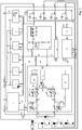
- a device for radiated interference-compensated control of a photodiode and for evaluating the photocurrent has two connections.
- the receiving diode D is operated between these.
- the receiving diode D is energized by two controlled current sources 27, 28 via the circuit nodes 61, 62.
- Two amplifiers 26, 29 detect the potentials on the input lines 30, 31 emanating from the connections. If the working point of the diode changes, for example due to permanent exposure to sunlight, the generated photocurrent changes. The voltage drop across the receiving diode D changes and so does the working potentials of the input lines 30, 31 and thus at the inputs of the amplifiers 26, 29. This is registered by the amplifiers 26, 29.
- the device according to the invention and the method according to the invention are based on the knowledge that in most applications, in particular in connection with gesture control for mobile devices, permanent measuring operation is not necessary or desirable at all. Such an operation consumes energy, which is extremely “valuable”, especially in the case of mobile devices, because it is only available to a limited extent.
- the device should therefore be in different system states as a function of time, i. H. operated in individual, time-separated and successive measurement intervals, each of which has at least one measurement phase.
- this measurement state the readjustment by the current sources 27, 28 is practically switched off. Only the capacitors 24, 25 hold the respective operating points. This is to be equated with a change in the internal resistance of the current sources 27, 28.
- the result of the respective measurement is typically temporarily stored in a sample-and-hold circuit (not shown).
- 16 states of the system of two measuring amplifiers 18, 19 with two evaluation signals each are possible. Not all of these make sense because, for example, simultaneous overdrive and underdrive is not realistic, but is nevertheless faulty.
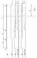
- the sequence of a measuring interval is shown, for example, by the digital control block 4 of the (block) circuit diagram Fig. 1 controlled.
- a measurement activation signal "Measure” (reference numeral 66, Fig. 2 ) at the beginning of the measurement (reference number 67, Fig. 2 ) activated.
- the power sources regulate 27.28 low resistance to the operating point of the receiving diode D.
- the output of the power supply for a compensation diode K is switched to active.
- the compensation diode K already irradiates the photodiode D.
- the compensation diode K is initially not modulated. Due to the low resistance of the current sources 27, 28, the measuring amplifiers 18, 19 quickly reach their operating points.
- the capacitances 20,21 or coupling capacitors 24,25 are charged to their working level.
- the current sources 64, 65, 66, 67 for the operation of three measuring transmitter diodes H1, H2, H3 in this exemplary embodiment (because of the multi-dimensional, in particular 3D gesture recognition) and the compensation diode K are set to the respective operating values.
- phase A At the end of phase A at time 69 ( Fig. 2 ) the signal "hold” (see reference numeral 68, Fig. 2 ) active.
- the voltage-controlled current sources 27, 28 go from their previously assumed low-resistance state to a high-resistance state. This "freezes” your operating points.
- the difference signal 63 of the outputs of the measuring amplifiers 18, 19 should be constant zero, since the operating points are adjusted.
- the modulation signals 45, 46, 47, 48 for the compensation diode K or for the measuring transmitter diodes H1, H2, H3 are square-wave signals which are phase-shifted by 180 ° and which can be regulated in amplitude. (see in measurement phase C Fig. 2 )
- the measurement begins by, for example, weakening or even switching off the radiation from the compensation diode (see reference symbols 45 and 69 in FIG Figs. 1 and 2 ).
- at least one of the transmission signals (see reference numeral 46 and / or 46 and / or 47 in FIG Figs. 1 and 2 ) switched on.
- the typically at least one measuring transmitter diode H1 and / or H2 and / or H3 irradiates the (receiving) photodiode D indirectly via the transmission path to be measured.
- the compensation transmitter diode K and the typically at least one measurement transmitter diode H1 or H2 or H3 are alternately weakened or caused to emit more intensely. Initially, this will lead to a remaining modulation of the output signal of the input stage. After amplification by an amplifier 36, the modulated signal received in this way can be converted into a DC signal with a demodulator. This can be used to regulate the amplitude of the modulation of one measurement transmitter diode or one of the transmitter diodes H1, H2, H3 and / or the amplitude of the modulation of the compensation diode K in each case.
- a regulation of the compensation diode K is shown as case F1 and a regulation of the measurement transmitter diode or diodes H1, H2, H3 as case F2.
- the regulation can be different for the measuring diodes H1, H2 and H3.
- the measurement transmitter diodes H1, H2 and H3 are typically not operated simultaneously but with a time delay. More than one receiving diode can also be used.
- the time offset is typically chosen so that only one receiving diode D and one transmitting diode H1, H2, H3 are active at the same time.
- the measured value obtained in this way readjusts the amplitude of the respective measurement transmitter diode H1, H2, H3. It has been shown that it makes sense to increase this value before the negative feedback. This principle is also known from operational amplifier circuits and is used to suppress parasitic factors and influences.
- DE-B-103 46 741 EP-A-2 546 620 , EP-A-2,356,000 , EP-B-1 410 507 , EP-B-1 435 509 , EP-A-2 418 512 , EP-B-1,269,629 , DE-A-103 22 552 , DE-B-10 2004 025 345 , EP-A-2 405 283 , DE-C-44 11 773 , WO-A-2012/163725 , DE-A-2006 020 579 , DE-B-10 2005 045 993 , EP-B-1 979 764 , DE-A-10 2012 024 778 , DE-A-10 2013 000 376 , DE10 2013 003 791.3 , DEA-10 2013 000 380 , WO-A-2014/096385 , WO-A-2013/124018
- the regulation creates an equilibrium and the output signal 50 of the demodulator 37 represents a measure of the attenuation of the transmission signal in the transmission channel after the amplification mentioned.
- the inventive control of the current sources 27, 28 is noticeable on the input lines 30, 31 in an input resistance to the effect that the current sources are activated depending on typically at least two phases of a measurement cycle (reference symbols A and C, B and C or A and B and C of the Fig. 2 ) fluctuate.
- the effectiveness of the voltage-controlled current sources 27, 28 is limited by the real conditions.
- the current sources 27, 28 can only try to maintain the respectively specified voltage level up to a maximum current.
- the measurement interval (from reference number 67, Fig. 2 , to reference number 71, Fig. 2 ) is ended in that the "Measure" signal (66) at the end of the measuring cycle (see reference numeral 71, Fig. 2 ) becomes inactive again. All transmission signals are switched off and the measurement result is typically frozen in a sample-and-hold circuit (not shown), for example.
- Measurement interval (from reference number 67, Fig. 2 , to reference number 71, Fig. 2 ) to be repeated at shorter or longer intervals.
- Measurement interval from reference number 67, Fig. 2 , to reference number 71, Fig. 2
- higher repetition frequencies for the measurement sequences result in higher power consumption.
- the system can be enabled to provide at least some and typically every measured value with a quality value of the measurement, that is to say to determine the quality of the measurement signal.
- this measure forms an independent subject matter of the invention.
- a sequence of measured values with associated quality values is obtained, which allows a measured value estimator to estimate an optimized measured value and to indicate a probability of the correctness of this measured value.
- the resulting measured value vector can be used, for example, as a basis for the feature extraction of a gesture recognition.
- an interferer does not modulate at a relatively low frequency, such as sunlight, (for example due to shading by trees, for example), but rather quickly, as is the case with fluorescent tubes or when driving in a convertible under trees in the sunshine will.
- a relatively low frequency such as sunlight, (for example due to shading by trees, for example)
- fluorescent tubes or when driving in a convertible under trees in the sunshine will.
- the interference frequency is in the vicinity of the modulation frequency of the measuring transmitter diodes H1, H2, H3 and of the compensation transmitter K, this frequency is usually not hit correctly.
- There is a beating in the control signal which can be recognized and used.
- the quality of the measurement will typically fluctuate with the beat frequency as a function of time.
- the system since, as a result of the evaluation of the measurement results, the system only evaluates measurement value sequences that are relatively undisturbed, the measurement signal is de facto automatically sampled only at times that are relatively undisturbed.
- the measurement signal is de facto automatically sampled only at times that are relatively undisturbed.
- an estimator determines a high probability of disturbance. This can for example be directly preceding or directly following measured values.
- Such a measuring system should also initiate countermeasures when faults are detected.
- the circuit can also be parameterized differently. For example, the time constants of the measuring amplifiers 18, 19 acting as integrators can be changed in that the capacitances 20, 21 can be changed. In the extreme case, the integrators can be bridged by bridging their capacitances 20, 21 with the aid of the programmable switches 22, 23. As you can see from this example, a change in the system or circuit topology is also an option. The integrators then become pure impedance converters.
- a further improvement of the device can therefore be achieved by assessing the quality of the measurement signal and / or by regulating to optimize the measurement results.
- the feedback loop is closed by software, since the control algorithms are very application-dependent.
- a change in the system parameters and / or the system topology or structure is typically used as an actuator for this measurement signal quality control.
- the current supplied by the current source or current sources 27, 28 is measured as a function of time in block 16 (“extrinsic light measurement” or “measurement of the external light”).
- exa Fourier transformation can be used to determine the interference frequencies that interfere with the measurement signal. It is particularly advantageous to adjust the modulation frequency of the measuring transmitter diodes H1, H2, H3 and the Compensation diode K and the repetition frequency of the measuring intervals (reference numeral 67, Fig. 2 , to reference number 71, Fig. 2 ) to be selected in such a way that they do not interfere with the interference frequencies as far as possible.
- the interference signal robustness can be increased by "frequency hopping".
- Such possible transmission signals are, for example, suitable pseudo-random sequences (see also EP-A-2 631 674 , the content of which is hereby the subject of the present application by reference)
- Another measure representing an independent inventive concept is the introduction and / or raising of a threshold for the detection of the approach of an object to the measuring transmitter diodes H1, H2, H3 / receiving diode D.
- This is a non-linear filter function, which is typically in block 37 the Fig. 1 is realized, but can also be realized in a subsequent processing stage. All measured values below or above a threshold are fixed, for example, to a predefined value.
- a computational model of an interferer can be parameterized and points in time and setting parameters for the measuring system can be predicted with which the next measuring interval can be carried out with particularly good quality.
- the circuit according to Fig. 1 has such an interface 53 (see in Fig. 1 top right), which is provided with a corresponding input hardware 7.
- the interface has, for example, a serial TX and RX two-wire line or an I 2 C bus interface 54, an interrupt output 55 for the main processor, which must be at a defined potential, a non-maskable measuring system reset 56 and a reference voltage input 57. All other systems are switched off. If possible, the normal system oscillator 6 is also switched off and instead this function block 14 of the circuit with a low frequency from a minimum oscillator 5 supplied. This is much smaller because it doesn't have to drive the entire IC.
- band gap reference 2 the block 4 (digital control), the voltage regulator 1 and all measuring amplifiers and receiving and transmitting devices are switched off.
- the interface 54 is, for example, an I 2 C interface, it makes sense to design the function block 14 so that it can only recognize a very specific command on the bus that is sent to a precisely specified register address.
- Such a protocol can for example be such that the function block 14 recognizes a sequence of a start bit and the slave address and a bit for signaling a write access and then outputs an acknowledge bit, whereupon the main processor sends the register address, the function block 14 sends an acknowledge bit and the main processor then sends a parity bit. If the function block 14 has recognized all of these data as correct, the voltage regulator, the bandgap reference 2 and all other parts of the circuit are started up in a predefined sequence one after the other and / or in parallel, depending on the type and requirement. The normal I 2 C bus communication is then taken over again by block 4 (digital control) until the next sleep command.
- block 4 (digital control) causes the essential parts of the measuring system to switch to energy-saving mode.
- the last part of the shutdown sequence must be controlled by function block 14. This applies in particular to the switching off of the energy supply by switching off the voltage regulator 1, the oscillator 6 and the block 4 (digital control) itself.
- the function block 14 has an internal timer that can wake up the system at regular intervals, without the need to receive a command from the main processor via the interface 54 for this purpose.
- the measured values and preferably also the measured value qualities are stored in a memory (not shown).
- the measured values stored there can also include configuration data of the system (for example with which of the transmitting diodes H1, H2, H3, with which of the compensation diode K and with which receiving diode D, when and with what quality measured values were recorded for example of block 16 (Extrinsic Light Measurement).
- the bandgap reference 2 which only supplies a reference voltage for use at different points in the measuring system, can be temporarily switched off if its voltage is temporarily stored and buffered in a sample-and-hold circuit, for example.
- the bandgap circuit is then only switched on from time to time to renew the inevitably slowly draining charges from the storage element of the sample-and-hold circuit (typically a capacitor).
- Another independently essential feature of the device results from the necessary calibration of the measuring system.
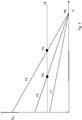
- Fig. 3 the control characteristics of the system with control of the transmitter diode amplitude T i are shown.
- the amplitude of the portion to be traced back to the respective measuring transmitter diode H1, H2, H3 (see 72,75,77 in Fig. 3 ) of The photocurrent I PD in the / a receiving diode D depends on the transmitting diode amplitude T i .
- the amplitude of the component to be traced back to the compensation diode K or the respective compensation diode K (see line 73 in Fig. 3 ) of the photocurrent I PD in the / a receiving diode D does not depend on the transmitter amplitude T i.
- the difference signal 63 is a constant signal.
- the portion to be traced back to the transmission signal is then zero in the difference signal 63.
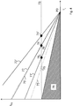
- the maximum distance from which an object approaching the receiving diode or up to which an object moving away from the receiving diode can still be recognized is determined by the control characteristic and / or the fact that at the maximum amplitude of the transmitting diode signal from the object there is still a so large a portion of the transmitting diode signal is reflected that a signal with at least the amplitude of the compensation diode signal is received at the receiving diode.
- a large photocurrent 72 which is synonymous with a nearby object (and thus for a steep control characteristic)
- there is a first working point 74 as an intersection with 73.
- the offset signal does not lead to one more achievable area 79 in the diagram of Fig. 4 .
- the generation of this offset signal is in Fig. 1 indicated by a calibration block 81 which generates the offset signal 82 for the respective transmitter / receiver combination from the transmitter signals 9 to 12, from which the signal 82 is generated by addition.
- the overall system differs from the measuring system, for example, in that, in addition to the measuring system, it also includes optical elements such as mirrors, diaphragms, etc. and of course the housing.
- the compensation diode K is switched to a static level.
- the coupling between receiving diode D and compensation diode K can only be stabilized with great difficulty. Therefore, the coupling is always to be assumed to be the same for one application type, but to vary from application to application within the same type.
- the calibration now takes place in such a way that the switchable reference current sources 41, 42, 43 are provided, with which the reference current supply 38 is now set so that the measured photocurrent is always set to the same, application-specific predetermined value.
- This allows the ordinate position of the line 73 in the Figs. 3 and 4th can be specified. This ensures that an operating point is found.
- This operating point is typically set in such a way that the compensation transmitting diode current is increased until the compensation signal can be measured above the system noise.
- the offset signal is then set to such a value that the lowest operating point is assumed.
Claims (10)
- Dispositif à compensation de rayonnement parasite destiné à mesurer un trajet de transmission de signal optique pendant une pluralité d'intervalles de mesure consécutifs, en particulier intermittents, en particulier pour la reconnaissance d'un objet et/ou pour la reconnaissance d'un mouvement et/ou d'une direction de mouvement d'un objet, doté- d'au moins un émetteur de mesure (H1, H2, H3) destiné à émettre un signal de mesure optique,- d'au moins un récepteur (D) destiné à recevoir un signal optique, dans lequel l'au moins un récepteur (D) est exposé à un rayonnement parasite provenant par exemple de l'environnement,- d'une unité de commande et d'évaluation (17) destinée à commander l'au moins un émetteur de mesure (H1, H2, H3) et l'au moins un récepteur (D) en vue d'émettre ou de recevoir un signal optique pendant une phase de mesure (C) d'un intervalle de mesure et destinée à évaluer le signal de mesure optique reçu par traitement d'un signal électrique, lequel agit sur un premier nœud de commutation (61, 62) couplé électriquement à l'au moins un récepteur (D) et est amplifié au moyen d'un amplificateur de mesure (18, 19), et- d'au moins une première unité de compensation de rayonnement parasite (26, 27, 28, 29) couplée au premier nœud de commutation (61, 62) destiné à la polarisation de l'au moins un récepteur (D) par fourniture d'un premier courant de compensation avec une grandeur qui est sensiblement égale à la grandeur d'un signal parasite produit par l'au moins un récepteur (D) à la suite du rayonnement parasite,caractérisé par- une unité fonctionnelle (14) destinée à faire passer l'au moins un émetteur de mesure (H1, H2, H3) et l'au moins une première unité de compensation de rayonnement parasite (26, 27, 28, 29) dans un mode de veille, où seuls l'unité fonctionnelle (14) et un oscillateur système (6) sont actifs et l'au moins un émetteur de mesure (H1, H2, H3) et l'au moins une première unité de compensation de rayonnement parasite (26, 27, 28, 29) sont éteints.
- Dispositif à compensation de rayonnement parasite selon la revendication 1, caractérisé en ce que l'au moins un récepteur (D) est commuté entre le premier nœud de commutation (61, 62) et un deuxième nœud de commutation (61, 62), avec lesquels il est respectivement couplé électriquement, dans lequel l'au moins une première unité de compensation de rayonnement parasite (26, 27) est couplée au premier nœud de commutation (61), en ce que les signaux électriques agissant sur et/ou entre ces nœuds de commutation (61, 62) peuvent être conduits à l'unité de commande et d'évaluation (17) et en ce qu'au moins une deuxième unité de compensation de rayonnement parasite (28, 29) avec une résistance interne variable, laquelle fournit un deuxième courant de compensation, lequel est sensiblement égal au premier courant de compensation, et en ce que l'unité fonctionnelle (14) en mode de veille désactive également la deuxième unité de compensation de rayonnement parasite (28, 29).
- Dispositif à compensation de rayonnement parasite selon la revendication 1 ou 2, caractérisé en ce que l'unité fonctionnelle (14) est raccordée à un bus et reconnaît un ordre envoyé à une adresse de registre prédéterminée sur le bus pour la commutation du fonctionnement normal au mode de veille et inversement.
- Dispositif à compensation de rayonnement parasite selon l'une des revendications 1 à 3, caractérisé en ce que l'unité fonctionnelle (14) comporte un temporisateur interne, lequel réveille le dispositif à intervalles de temps réguliers.
- Dispositif à compensation de rayonnement parasite selon l'une des revendications 1 à 4, caractérisé par une commande de délai destinée à la commande de l'unité fonctionnelle (14) afin de passer du fonctionnement normal au mode de veille, à savoir après l'exécution de tâches de mesure et/ou de tâches pré-définissables et/ou réglables.
- Dispositif à compensation de rayonnement parasite selon l'une des revendications 1 à 5, caractérisé par au moins une référence à bande interdite (2), laquelle est temporairement activable uniquement par une commande de délai (4) et dont les valeurs de sortie analogiques peuvent être mises en mémoire tampon en particulier dans un circuit échantillonneur-bloqueur.
- Dispositif à compensation de rayonnement parasite selon l'une des revendications 1 à 6, caractérisé par au moins une référence à bande interdite (2), laquelle est temporairement activable uniquement par une commande de délai (4) et dont les valeurs de sortie analogiques sont mises en mémoire tampon en particulier dans un circuit échantillonneur-bloqueur pendant une activation du mode de veille de la référence à bande interdite (2) commandée par l'unité fonctionnelle (14).
- Dispositif à compensation de rayonnement parasite selon l'une des revendications 1 à 7, caractérisé par au moins une référence à bande interdite (2), laquelle est éteinte dans un mode de veille déclenché par l'unité fonctionnelle (14).
- Dispositif à compensation de rayonnement parasite selon l'une des revendications 1 à 8, caractérisé par au moins un régulateur de tension (1) destiné à l'alimentation d'au moins des parties du dispositif en énergie électrique, dans lequel le régulateur de tension (1), commandé par l'unité fonctionnelle (14), est éteint dans un mode de veille.
- Dispositif à compensation de rayonnement parasite selon l'une des revendications 1 à 9, caractérisé par une activation uniquement temporaire au moyen d'un signal externe de bande interdite et une mise en mémoire tampon de valeurs de sortie analogiques en particulier dans un circuit échantillonneur-bloqueur pendant le mode de veille activé par l'unité fonctionnelle (14) pour une référence à bande interdite (2), dans lequel le mode de veille peut être éteint sur commande par un signal externe de bande interdite.
Applications Claiming Priority (3)
| Application Number | Priority Date | Filing Date | Title |
|---|---|---|---|
| EP2013067480 | 2013-08-22 | ||
| PCT/EP2014/067851 WO2015025014A1 (fr) | 2013-08-22 | 2014-08-21 | Dispositif à compensation d'effets parasites pour mesurer un trajet de transmission optique |
| EP14753260.0A EP3036561B1 (fr) | 2013-08-22 | 2014-08-21 | Dispositif à compensation d'effets parasites pour mesurer un trajet de transmission optique |
Related Parent Applications (2)
| Application Number | Title | Priority Date | Filing Date |
|---|---|---|---|
| EP14753260.0A Division EP3036561B1 (fr) | 2013-08-22 | 2014-08-21 | Dispositif à compensation d'effets parasites pour mesurer un trajet de transmission optique |
| EP14753260.0A Division-Into EP3036561B1 (fr) | 2013-08-22 | 2014-08-21 | Dispositif à compensation d'effets parasites pour mesurer un trajet de transmission optique |
Publications (2)
| Publication Number | Publication Date |
|---|---|
| EP3124993A1 EP3124993A1 (fr) | 2017-02-01 |
| EP3124993B1 true EP3124993B1 (fr) | 2021-10-06 |
Family
ID=56024450
Family Applications (2)
| Application Number | Title | Priority Date | Filing Date |
|---|---|---|---|
| EP14753260.0A Active EP3036561B1 (fr) | 2013-08-22 | 2014-08-21 | Dispositif à compensation d'effets parasites pour mesurer un trajet de transmission optique |
| EP16187776.6A Active EP3124993B1 (fr) | 2013-08-22 | 2014-08-21 | Dispositif a compensation de defaut destine a mesurer une voie d'acheminement de signaux optiques |
Family Applications Before (1)
| Application Number | Title | Priority Date | Filing Date |
|---|---|---|---|
| EP14753260.0A Active EP3036561B1 (fr) | 2013-08-22 | 2014-08-21 | Dispositif à compensation d'effets parasites pour mesurer un trajet de transmission optique |
Country Status (1)
| Country | Link |
|---|---|
| EP (2) | EP3036561B1 (fr) |
Family Cites Families (29)
| Publication number | Priority date | Publication date | Assignee | Title |
|---|---|---|---|---|
| DE9309837U1 (de) | 1993-07-02 | 1993-09-02 | Reime Gerd | Anordnung zum Messen oder Erkennen der Benetzung einer für eine bestimmte Strahlung durchlässigen Wand oder Platte |
| DE10001955A1 (de) | 2000-01-18 | 2001-07-19 | Gerd Reime | Opto-elektronischer Schalter |
| DE10133823A1 (de) | 2001-07-16 | 2003-02-27 | Gerd Reime | Optoelektronische Vorrichtung zur Positions- und Bewegungserfassung sowie zugehöriges Verfahren |
| DE10256429A1 (de) | 2002-12-02 | 2004-06-24 | Gerd Reime | Verfahren und Anordnung zum Messen eines modulierten Lichtsignals |
| DE10300224A1 (de) | 2003-01-03 | 2004-07-22 | Gerd Reime | Optoelektronische Messanordnung sowie damit versehener Drehknopf |
| DE10300223B3 (de) | 2003-01-03 | 2004-06-24 | Gerd Reime | Optoelektronische Messanordnung mit Fremdlichtkompensation sowie Verfahren zur phasenkorrekten Kompensation eines Signals der Messanordnung |
| DE10322552A1 (de) | 2003-05-20 | 2004-12-30 | Gerd Reime | Verfahren und Vorrichtung zum Messen eines modulierten Lichtsignals |
| DE10346741B3 (de) | 2003-10-08 | 2005-03-24 | Mechaless Systems Gmbh | Verfahren zur Bestimmung und/oder Auswertung eines differentiellen optischen Signals |
| DE102004025345B3 (de) | 2004-05-19 | 2005-11-03 | Daimlerchrysler Ag | Vorrichtung und Verfahren zum Erkennen eines Objekts in oder an einer verschließbaren Öffnung |
| DE102005045993B4 (de) | 2005-07-29 | 2008-11-13 | Gerd Reime | Verfahren zur Lichtlaufzeitmessung |
| DE102006003269A1 (de) | 2006-01-24 | 2007-07-26 | Mechaless Systems Gmbh | Verfahren zur Lichtlaufzeitmessung |
| DE102006020579A1 (de) | 2006-05-03 | 2007-11-08 | BSH Bosch und Siemens Hausgeräte GmbH | Verfahren und Schaltungsanordnung zum Steuern eines Trock-nungsprozesses eines Hausgeräts zur Pflege von Wäschestücken |
| EP2356000B1 (fr) | 2008-11-20 | 2013-01-02 | ELMOS Semiconductor AG | Détecteur à compensation de perturbation |
| EP2405283B1 (fr) | 2010-07-06 | 2014-03-05 | Mechaless Systems GmbH | Agencement de mesure optoélectronique doté d'une source lumineuse de compensation |
| EP2418512A1 (fr) | 2010-07-30 | 2012-02-15 | Mechaless Systems GmbH | Agencement de mesure optoélectronique doté d'une compensation de lumière parasite |
| DE112012002330A5 (de) | 2011-05-31 | 2014-03-20 | Mechaless Systems Gmbh | Display mit integriertem optischen Sender |
| EP2546620B1 (fr) | 2011-07-13 | 2014-04-09 | ELMOS Semiconductor AG | Dispositif de compensation de la lumière ambiante pour une lumière utile uniforme et capteurs optiques soumis à la lumière ambiante |
| EP2597482A1 (fr) | 2011-11-22 | 2013-05-29 | ELMOS Semiconductor AG | Dispositif et capteur de mesure d'éloignement à l'aide de la durée de fonctionnement d'impulsions compensées |
| EP2631674A1 (fr) | 2012-02-23 | 2013-08-28 | ELMOS Semiconductor AG | Procédé et système de capteur destinés à la mesure des propriétés d'une voie de transmission d'un système de mesure entre émetteur et récepteur |
| EP2653885A1 (fr) | 2012-04-18 | 2013-10-23 | ELMOS Semiconductor AG | Système de capteur et procédé destinés à la mesure des propriétés de transmission d'une voie de transmission d'un système de mesure entre un émetteur et un récepteur |
| DE102012024778A1 (de) | 2012-05-23 | 2013-11-28 | Elmos Semiconductor Ag | Kontinuierlich arbeitende, berührungslose, optische Gestenerkennungsvorrichtung |
| DE102012025564A1 (de) | 2012-05-23 | 2013-11-28 | Elmos Semiconductor Ag | Vorrichtung und Verfahren zur Kalibration einer kalibrierbaren Gestenerkennungsvorrichtung zur Übermittlung von Kommandos und Informationen an eine Mensch-Maschineschnittstelle |
| EP2679982B1 (fr) | 2012-06-28 | 2020-05-06 | Elmos Semiconductor Aktiengesellschaft | Système de capteur et procédé destinés à la mesure des propriétés de transmission d'une voie de transmission d'un système de mesure entre un émetteur et un récepteur |
| EP3594724B1 (fr) | 2012-11-09 | 2021-07-21 | Elmos Semiconductor SE | Bobine pour un capteur inductif et circuit de commande d'un tel capteur inductif |
| DE102012024597B4 (de) | 2012-12-13 | 2014-07-24 | Elmos Semiconductor Ag | Zeitauflösendes Verzögerungsmesssystem |
| EP2936201B1 (fr) | 2012-12-21 | 2020-04-15 | Elmos Semiconductor Aktiengesellschaft | Dispositif de détermination d'une propriété d'un canal de transmission entre un émetteur et un récepteur |
| DE102013000376A1 (de) | 2013-01-07 | 2014-07-10 | Elmos Semiconductor Ag | Vorrichtung zur optischen Messung biometrischer Parameter eines Wirbeltieres oder Menschen |
| DE102013002304B3 (de) | 2013-02-05 | 2014-03-20 | Elmos Semiconductor Ag | Optisches Sensorsystem für ein Automobil zur Erfassung des Straßenzustands |
| DE102013002676B4 (de) | 2013-02-12 | 2023-06-29 | Elmos Semiconductor Se | Kompensiertes Sensorsystem mit einem in der Sensitivität regelbaren Empfänger als kompensierendes Element |
-
2014
- 2014-08-21 EP EP14753260.0A patent/EP3036561B1/fr active Active
- 2014-08-21 EP EP16187776.6A patent/EP3124993B1/fr active Active
Non-Patent Citations (1)
| Title |
|---|
| None * |
Also Published As
| Publication number | Publication date |
|---|---|
| EP3124993A1 (fr) | 2017-02-01 |
| EP3036561B1 (fr) | 2018-01-31 |
| EP3036561A1 (fr) | 2016-06-29 |
Similar Documents
| Publication | Publication Date | Title |
|---|---|---|
| EP1622257B1 (fr) | Amplificateur pour convertir un signal de courant d'un récepteur optique en un signal de tension | |
| DE102015204021B4 (de) | Dynamische Strombegrenzungsschaltung | |
| DE102007005187B4 (de) | Verfahren und Vorrichtung zur Bestimmung einer Entfernung zu einem rückstrahlenden Objekt | |
| DE102008044147B4 (de) | Empfangskomparator für Signalmodulation auf Versorgungsleitung | |
| DE102014013506B4 (de) | Schutz eines NFC- oder RFID-Funksystems bei Vorhandensein von starken elektromagnetischen Feldern | |
| DE19723645A1 (de) | Anordnung zur Signalübertragung zwischen einer Geberstelle und einer Empfangsstelle | |
| DE102010030678B4 (de) | Zeitverzögerungskompensation und Impulsbreitenkorrektur | |
| EP1545029A2 (fr) | Dispositif de réception optique | |
| EP1545028B1 (fr) | Récepteur optique avec dispositif de commande avec un largeur de bande variable | |
| DE102014019983B3 (de) | Sensorschnittstellensysteme und -verfahren | |
| DE112021005775T5 (de) | Einrichtungen und verfahren zum parallelisieren von transistoren | |
| EP2953247A1 (fr) | Appareil de terrain doté d'une alimentation à découpage | |
| EP3124993B1 (fr) | Dispositif a compensation de defaut destine a mesurer une voie d'acheminement de signaux optiques | |
| DE10025834A1 (de) | Einrichtung und Verfahren zur Erzeugung von Hochspannung aus einer Niedervolt-Versorgungsquelle | |
| DE1264538B (de) | Radarsystem zur automatischen Entfernungsbestimmung | |
| WO2015025014A1 (fr) | Dispositif à compensation d'effets parasites pour mesurer un trajet de transmission optique | |
| DE202014002367U1 (de) | „Dynamische Hysterese"-Komparator | |
| EP3036560B1 (fr) | Procédé d'étalonnage d'un dispositif de mesure d'une ligne de transmission de signaux optiques | |
| DE60122646T2 (de) | Signalkompensierungsschaltung und Demodulatorschaltung | |
| EP3036559B1 (fr) | Dispositif permettant de mesurer un chemin optique de transmission | |
| EP3586272B1 (fr) | Transpondeur bidirectionnel à faible consommation d'énergie | |
| DE102010024128A1 (de) | Wechselspannungssteller | |
| WO2015025011A1 (fr) | Dispositif permettant de mesurer un chemin optique de transmission | |
| DE102014000345A1 (de) | Empfangsschaltung für Stromleitungsträgerkommunikation | |
| DE102018106762B4 (de) | Analoger front-end-empfänger mit grossem dynamikbereich für long-range-lidar |
Legal Events
| Date | Code | Title | Description |
|---|---|---|---|
| PUAI | Public reference made under article 153(3) epc to a published international application that has entered the european phase |
Free format text: ORIGINAL CODE: 0009012 |
|
| STAA | Information on the status of an ep patent application or granted ep patent |
Free format text: STATUS: THE APPLICATION HAS BEEN PUBLISHED |
|
| AC | Divisional application: reference to earlier application |
Ref document number: 3036561 Country of ref document: EP Kind code of ref document: P |
|
| AK | Designated contracting states |
Kind code of ref document: A1 Designated state(s): AL AT BE BG CH CY CZ DE DK EE ES FI FR GB GR HR HU IE IS IT LI LT LU LV MC MK MT NL NO PL PT RO RS SE SI SK SM TR |
|
| AX | Request for extension of the european patent |
Extension state: BA ME |
|
| STAA | Information on the status of an ep patent application or granted ep patent |
Free format text: STATUS: REQUEST FOR EXAMINATION WAS MADE |
|
| 17P | Request for examination filed |
Effective date: 20170719 |
|
| RBV | Designated contracting states (corrected) |
Designated state(s): AL AT BE BG CH CY CZ DE DK EE ES FI FR GB GR HR HU IE IS IT LI LT LU LV MC MK MT NL NO PL PT RO RS SE SI SK SM TR |
|
| STAA | Information on the status of an ep patent application or granted ep patent |
Free format text: STATUS: EXAMINATION IS IN PROGRESS |
|
| 17Q | First examination report despatched |
Effective date: 20190927 |
|
| STAA | Information on the status of an ep patent application or granted ep patent |
Free format text: STATUS: EXAMINATION IS IN PROGRESS |
|
| RAP1 | Party data changed (applicant data changed or rights of an application transferred) |
Owner name: ELMOS SEMICONDUCTOR SE |
|
| REG | Reference to a national code |
Ref country code: DE Ref legal event code: R079 Ref document number: 502014015928 Country of ref document: DE Free format text: PREVIOUS MAIN CLASS: G01S0007497000 Ipc: G01S0017040000 |
|
| RIN1 | Information on inventor provided before grant (corrected) |
Inventor name: JOERGER, WOLFGANG Inventor name: KILIAN, MARKUS Inventor name: STELLBERGER, ACHIM Inventor name: HUELSS, ROLF |
|
| GRAP | Despatch of communication of intention to grant a patent |
Free format text: ORIGINAL CODE: EPIDOSNIGR1 |
|
| STAA | Information on the status of an ep patent application or granted ep patent |
Free format text: STATUS: GRANT OF PATENT IS INTENDED |
|
| RIC1 | Information provided on ipc code assigned before grant |
Ipc: G01S 7/497 20060101ALI20210226BHEP Ipc: G01S 17/04 20200101AFI20210226BHEP Ipc: G01S 7/486 20200101ALI20210226BHEP |
|
| INTG | Intention to grant announced |
Effective date: 20210317 |
|
| GRAS | Grant fee paid |
Free format text: ORIGINAL CODE: EPIDOSNIGR3 |
|
| GRAA | (expected) grant |
Free format text: ORIGINAL CODE: 0009210 |
|
| STAA | Information on the status of an ep patent application or granted ep patent |
Free format text: STATUS: THE PATENT HAS BEEN GRANTED |
|
| AC | Divisional application: reference to earlier application |
Ref document number: 3036561 Country of ref document: EP Kind code of ref document: P |
|
| AK | Designated contracting states |
Kind code of ref document: B1 Designated state(s): AL AT BE BG CH CY CZ DE DK EE ES FI FR GB GR HR HU IE IS IT LI LT LU LV MC MK MT NL NO PL PT RO RS SE SI SK SM TR |
|
| REG | Reference to a national code |
Ref country code: GB Ref legal event code: FG4D Free format text: NOT ENGLISH |
|
| REG | Reference to a national code |
Ref country code: CH Ref legal event code: EP Ref country code: AT Ref legal event code: REF Ref document number: 1436686 Country of ref document: AT Kind code of ref document: T Effective date: 20211015 |
|
| REG | Reference to a national code |
Ref country code: IE Ref legal event code: FG4D Free format text: LANGUAGE OF EP DOCUMENT: GERMAN |
|
| REG | Reference to a national code |
Ref country code: DE Ref legal event code: R096 Ref document number: 502014015928 Country of ref document: DE |
|
| REG | Reference to a national code |
Ref country code: LT Ref legal event code: MG9D |
|
| REG | Reference to a national code |
Ref country code: NL Ref legal event code: MP Effective date: 20211006 |
|
| PG25 | Lapsed in a contracting state [announced via postgrant information from national office to epo] |
Ref country code: RS Free format text: LAPSE BECAUSE OF FAILURE TO SUBMIT A TRANSLATION OF THE DESCRIPTION OR TO PAY THE FEE WITHIN THE PRESCRIBED TIME-LIMIT Effective date: 20211006 Ref country code: LT Free format text: LAPSE BECAUSE OF FAILURE TO SUBMIT A TRANSLATION OF THE DESCRIPTION OR TO PAY THE FEE WITHIN THE PRESCRIBED TIME-LIMIT Effective date: 20211006 Ref country code: FI Free format text: LAPSE BECAUSE OF FAILURE TO SUBMIT A TRANSLATION OF THE DESCRIPTION OR TO PAY THE FEE WITHIN THE PRESCRIBED TIME-LIMIT Effective date: 20211006 Ref country code: BG Free format text: LAPSE BECAUSE OF FAILURE TO SUBMIT A TRANSLATION OF THE DESCRIPTION OR TO PAY THE FEE WITHIN THE PRESCRIBED TIME-LIMIT Effective date: 20220106 |
|
| PG25 | Lapsed in a contracting state [announced via postgrant information from national office to epo] |
Ref country code: IS Free format text: LAPSE BECAUSE OF FAILURE TO SUBMIT A TRANSLATION OF THE DESCRIPTION OR TO PAY THE FEE WITHIN THE PRESCRIBED TIME-LIMIT Effective date: 20220206 Ref country code: SE Free format text: LAPSE BECAUSE OF FAILURE TO SUBMIT A TRANSLATION OF THE DESCRIPTION OR TO PAY THE FEE WITHIN THE PRESCRIBED TIME-LIMIT Effective date: 20211006 Ref country code: PT Free format text: LAPSE BECAUSE OF FAILURE TO SUBMIT A TRANSLATION OF THE DESCRIPTION OR TO PAY THE FEE WITHIN THE PRESCRIBED TIME-LIMIT Effective date: 20220207 Ref country code: PL Free format text: LAPSE BECAUSE OF FAILURE TO SUBMIT A TRANSLATION OF THE DESCRIPTION OR TO PAY THE FEE WITHIN THE PRESCRIBED TIME-LIMIT Effective date: 20211006 Ref country code: NO Free format text: LAPSE BECAUSE OF FAILURE TO SUBMIT A TRANSLATION OF THE DESCRIPTION OR TO PAY THE FEE WITHIN THE PRESCRIBED TIME-LIMIT Effective date: 20220106 Ref country code: NL Free format text: LAPSE BECAUSE OF FAILURE TO SUBMIT A TRANSLATION OF THE DESCRIPTION OR TO PAY THE FEE WITHIN THE PRESCRIBED TIME-LIMIT Effective date: 20211006 Ref country code: LV Free format text: LAPSE BECAUSE OF FAILURE TO SUBMIT A TRANSLATION OF THE DESCRIPTION OR TO PAY THE FEE WITHIN THE PRESCRIBED TIME-LIMIT Effective date: 20211006 Ref country code: HR Free format text: LAPSE BECAUSE OF FAILURE TO SUBMIT A TRANSLATION OF THE DESCRIPTION OR TO PAY THE FEE WITHIN THE PRESCRIBED TIME-LIMIT Effective date: 20211006 Ref country code: GR Free format text: LAPSE BECAUSE OF FAILURE TO SUBMIT A TRANSLATION OF THE DESCRIPTION OR TO PAY THE FEE WITHIN THE PRESCRIBED TIME-LIMIT Effective date: 20220107 Ref country code: ES Free format text: LAPSE BECAUSE OF FAILURE TO SUBMIT A TRANSLATION OF THE DESCRIPTION OR TO PAY THE FEE WITHIN THE PRESCRIBED TIME-LIMIT Effective date: 20211006 |
|
| REG | Reference to a national code |
Ref country code: DE Ref legal event code: R097 Ref document number: 502014015928 Country of ref document: DE |
|
| PG25 | Lapsed in a contracting state [announced via postgrant information from national office to epo] |
Ref country code: SM Free format text: LAPSE BECAUSE OF FAILURE TO SUBMIT A TRANSLATION OF THE DESCRIPTION OR TO PAY THE FEE WITHIN THE PRESCRIBED TIME-LIMIT Effective date: 20211006 Ref country code: SK Free format text: LAPSE BECAUSE OF FAILURE TO SUBMIT A TRANSLATION OF THE DESCRIPTION OR TO PAY THE FEE WITHIN THE PRESCRIBED TIME-LIMIT Effective date: 20211006 Ref country code: RO Free format text: LAPSE BECAUSE OF FAILURE TO SUBMIT A TRANSLATION OF THE DESCRIPTION OR TO PAY THE FEE WITHIN THE PRESCRIBED TIME-LIMIT Effective date: 20211006 Ref country code: EE Free format text: LAPSE BECAUSE OF FAILURE TO SUBMIT A TRANSLATION OF THE DESCRIPTION OR TO PAY THE FEE WITHIN THE PRESCRIBED TIME-LIMIT Effective date: 20211006 Ref country code: DK Free format text: LAPSE BECAUSE OF FAILURE TO SUBMIT A TRANSLATION OF THE DESCRIPTION OR TO PAY THE FEE WITHIN THE PRESCRIBED TIME-LIMIT Effective date: 20211006 Ref country code: CZ Free format text: LAPSE BECAUSE OF FAILURE TO SUBMIT A TRANSLATION OF THE DESCRIPTION OR TO PAY THE FEE WITHIN THE PRESCRIBED TIME-LIMIT Effective date: 20211006 |
|
| PLBE | No opposition filed within time limit |
Free format text: ORIGINAL CODE: 0009261 |
|
| STAA | Information on the status of an ep patent application or granted ep patent |
Free format text: STATUS: NO OPPOSITION FILED WITHIN TIME LIMIT |
|
| 26N | No opposition filed |
Effective date: 20220707 |
|
| PG25 | Lapsed in a contracting state [announced via postgrant information from national office to epo] |
Ref country code: AL Free format text: LAPSE BECAUSE OF FAILURE TO SUBMIT A TRANSLATION OF THE DESCRIPTION OR TO PAY THE FEE WITHIN THE PRESCRIBED TIME-LIMIT Effective date: 20211006 |
|
| PG25 | Lapsed in a contracting state [announced via postgrant information from national office to epo] |
Ref country code: SI Free format text: LAPSE BECAUSE OF FAILURE TO SUBMIT A TRANSLATION OF THE DESCRIPTION OR TO PAY THE FEE WITHIN THE PRESCRIBED TIME-LIMIT Effective date: 20211006 |
|
| PG25 | Lapsed in a contracting state [announced via postgrant information from national office to epo] |
Ref country code: MC Free format text: LAPSE BECAUSE OF FAILURE TO SUBMIT A TRANSLATION OF THE DESCRIPTION OR TO PAY THE FEE WITHIN THE PRESCRIBED TIME-LIMIT Effective date: 20211006 |
|
| REG | Reference to a national code |
Ref country code: CH Ref legal event code: PL |
|
| GBPC | Gb: european patent ceased through non-payment of renewal fee |
Effective date: 20220821 |
|
| PG25 | Lapsed in a contracting state [announced via postgrant information from national office to epo] |
Ref country code: LU Free format text: LAPSE BECAUSE OF NON-PAYMENT OF DUE FEES Effective date: 20220821 Ref country code: LI Free format text: LAPSE BECAUSE OF NON-PAYMENT OF DUE FEES Effective date: 20220831 Ref country code: CH Free format text: LAPSE BECAUSE OF NON-PAYMENT OF DUE FEES Effective date: 20220831 |
|
| REG | Reference to a national code |
Ref country code: BE Ref legal event code: MM Effective date: 20220831 |
|
| PG25 | Lapsed in a contracting state [announced via postgrant information from national office to epo] |
Ref country code: IT Free format text: LAPSE BECAUSE OF FAILURE TO SUBMIT A TRANSLATION OF THE DESCRIPTION OR TO PAY THE FEE WITHIN THE PRESCRIBED TIME-LIMIT Effective date: 20211006 |
|
| PG25 | Lapsed in a contracting state [announced via postgrant information from national office to epo] |
Ref country code: IE Free format text: LAPSE BECAUSE OF NON-PAYMENT OF DUE FEES Effective date: 20220821 |
|
| PG25 | Lapsed in a contracting state [announced via postgrant information from national office to epo] |
Ref country code: BE Free format text: LAPSE BECAUSE OF NON-PAYMENT OF DUE FEES Effective date: 20220831 |
|
| REG | Reference to a national code |
Ref country code: AT Ref legal event code: MM01 Ref document number: 1436686 Country of ref document: AT Kind code of ref document: T Effective date: 20220821 |
|
| PG25 | Lapsed in a contracting state [announced via postgrant information from national office to epo] |
Ref country code: GB Free format text: LAPSE BECAUSE OF NON-PAYMENT OF DUE FEES Effective date: 20220821 Ref country code: AT Free format text: LAPSE BECAUSE OF NON-PAYMENT OF DUE FEES Effective date: 20220821 |
|
| PGFP | Annual fee paid to national office [announced via postgrant information from national office to epo] |
Ref country code: FR Payment date: 20230822 Year of fee payment: 10 Ref country code: DE Payment date: 20230829 Year of fee payment: 10 |
|
| PG25 | Lapsed in a contracting state [announced via postgrant information from national office to epo] |
Ref country code: HU Free format text: LAPSE BECAUSE OF FAILURE TO SUBMIT A TRANSLATION OF THE DESCRIPTION OR TO PAY THE FEE WITHIN THE PRESCRIBED TIME-LIMIT; INVALID AB INITIO Effective date: 20140821 |