EP3124993B1 - Disturbance-compensated device for measuring an optical signal transfer route - Google Patents
Disturbance-compensated device for measuring an optical signal transfer route Download PDFInfo
- Publication number
- EP3124993B1 EP3124993B1 EP16187776.6A EP16187776A EP3124993B1 EP 3124993 B1 EP3124993 B1 EP 3124993B1 EP 16187776 A EP16187776 A EP 16187776A EP 3124993 B1 EP3124993 B1 EP 3124993B1
- Authority
- EP
- European Patent Office
- Prior art keywords
- interference
- radiation
- measurement
- signal
- receiver
- Prior art date
- Legal status (The legal status is an assumption and is not a legal conclusion. Google has not performed a legal analysis and makes no representation as to the accuracy of the status listed.)
- Active
Links
- 230000003287 optical effect Effects 0.000 title claims description 37
- 238000005259 measurement Methods 0.000 claims description 103
- 230000005855 radiation Effects 0.000 claims description 40
- 238000001514 detection method Methods 0.000 claims description 15
- 230000008054 signal transmission Effects 0.000 claims description 15
- 238000012545 processing Methods 0.000 claims description 7
- 230000004913 activation Effects 0.000 claims description 3
- 230000003139 buffering effect Effects 0.000 claims 1
- 238000011156 evaluation Methods 0.000 description 29
- 230000006870 function Effects 0.000 description 16
- 238000002360 preparation method Methods 0.000 description 15
- 230000005540 biological transmission Effects 0.000 description 12
- 239000003990 capacitor Substances 0.000 description 8
- 238000000034 method Methods 0.000 description 8
- 230000033228 biological regulation Effects 0.000 description 7
- 230000008859 change Effects 0.000 description 6
- 230000008878 coupling Effects 0.000 description 6
- 238000010168 coupling process Methods 0.000 description 6
- 238000005859 coupling reaction Methods 0.000 description 6
- 238000005265 energy consumption Methods 0.000 description 5
- 230000002829 reductive effect Effects 0.000 description 5
- 230000001276 controlling effect Effects 0.000 description 4
- 238000010586 diagram Methods 0.000 description 4
- 238000011161 development Methods 0.000 description 3
- 230000002452 interceptive effect Effects 0.000 description 3
- 230000001105 regulatory effect Effects 0.000 description 3
- 101100269674 Mus musculus Alyref2 gene Proteins 0.000 description 2
- 230000003321 amplification Effects 0.000 description 2
- 238000013459 approach Methods 0.000 description 2
- 238000004891 communication Methods 0.000 description 2
- 230000000295 complement effect Effects 0.000 description 2
- 238000013461 design Methods 0.000 description 2
- 238000003199 nucleic acid amplification method Methods 0.000 description 2
- 230000003071 parasitic effect Effects 0.000 description 2
- 230000035945 sensitivity Effects 0.000 description 2
- 101100390736 Danio rerio fign gene Proteins 0.000 description 1
- 101100537098 Mus musculus Alyref gene Proteins 0.000 description 1
- 101100390738 Mus musculus Fign gene Proteins 0.000 description 1
- 230000006978 adaptation Effects 0.000 description 1
- 101150095908 apex1 gene Proteins 0.000 description 1
- 230000004888 barrier function Effects 0.000 description 1
- 230000035559 beat frequency Effects 0.000 description 1
- 238000010009 beating Methods 0.000 description 1
- 238000005094 computer simulation Methods 0.000 description 1
- 230000001419 dependent effect Effects 0.000 description 1
- 230000000694 effects Effects 0.000 description 1
- 238000000605 extraction Methods 0.000 description 1
- 230000002349 favourable effect Effects 0.000 description 1
- 230000003760 hair shine Effects 0.000 description 1
- 230000001976 improved effect Effects 0.000 description 1
- 230000006872 improvement Effects 0.000 description 1
- 230000001939 inductive effect Effects 0.000 description 1
- 230000000977 initiatory effect Effects 0.000 description 1
- 238000012432 intermediate storage Methods 0.000 description 1
- 230000002093 peripheral effect Effects 0.000 description 1
- 238000001303 quality assessment method Methods 0.000 description 1
- 238000003908 quality control method Methods 0.000 description 1
- 238000011158 quantitative evaluation Methods 0.000 description 1
- 230000009467 reduction Effects 0.000 description 1
- 230000002441 reversible effect Effects 0.000 description 1
- 230000011664 signaling Effects 0.000 description 1
- 238000001228 spectrum Methods 0.000 description 1
- 230000007480 spreading Effects 0.000 description 1
- 230000006641 stabilisation Effects 0.000 description 1
- 238000011105 stabilization Methods 0.000 description 1
- 230000003068 static effect Effects 0.000 description 1
- 238000003860 storage Methods 0.000 description 1
- 230000001629 suppression Effects 0.000 description 1
- 230000001360 synchronised effect Effects 0.000 description 1
- 230000009466 transformation Effects 0.000 description 1
- 230000001960 triggered effect Effects 0.000 description 1
- 230000003313 weakening effect Effects 0.000 description 1
Images
Classifications
-
- G—PHYSICS
- G01—MEASURING; TESTING
- G01S—RADIO DIRECTION-FINDING; RADIO NAVIGATION; DETERMINING DISTANCE OR VELOCITY BY USE OF RADIO WAVES; LOCATING OR PRESENCE-DETECTING BY USE OF THE REFLECTION OR RERADIATION OF RADIO WAVES; ANALOGOUS ARRANGEMENTS USING OTHER WAVES
- G01S7/00—Details of systems according to groups G01S13/00, G01S15/00, G01S17/00
- G01S7/48—Details of systems according to groups G01S13/00, G01S15/00, G01S17/00 of systems according to group G01S17/00
- G01S7/497—Means for monitoring or calibrating
-
- G—PHYSICS
- G01—MEASURING; TESTING
- G01S—RADIO DIRECTION-FINDING; RADIO NAVIGATION; DETERMINING DISTANCE OR VELOCITY BY USE OF RADIO WAVES; LOCATING OR PRESENCE-DETECTING BY USE OF THE REFLECTION OR RERADIATION OF RADIO WAVES; ANALOGOUS ARRANGEMENTS USING OTHER WAVES
- G01S17/00—Systems using the reflection or reradiation of electromagnetic waves other than radio waves, e.g. lidar systems
- G01S17/02—Systems using the reflection of electromagnetic waves other than radio waves
- G01S17/04—Systems determining the presence of a target
-
- G—PHYSICS
- G01—MEASURING; TESTING
- G01S—RADIO DIRECTION-FINDING; RADIO NAVIGATION; DETERMINING DISTANCE OR VELOCITY BY USE OF RADIO WAVES; LOCATING OR PRESENCE-DETECTING BY USE OF THE REFLECTION OR RERADIATION OF RADIO WAVES; ANALOGOUS ARRANGEMENTS USING OTHER WAVES
- G01S7/00—Details of systems according to groups G01S13/00, G01S15/00, G01S17/00
- G01S7/48—Details of systems according to groups G01S13/00, G01S15/00, G01S17/00 of systems according to group G01S17/00
- G01S7/483—Details of pulse systems
- G01S7/486—Receivers
Definitions
- the invention relates to a radiation-compensated device for measuring an optical signal transmission path during a plurality of, in particular, intermittently successive measuring intervals, in particular for the detection of an object and / or for the detection of a movement and / or movement device of an object.
- a photodiode is typically operated in the reverse direction. It has proven to be particularly advantageous to energize the photodiode to compensate for a photocurrent resulting from (e.g. ambient) interference radiation by a voltage-controlled current source and to keep it at a voltage-related predetermined operating point.
- a particularly advantageous arrangement for measuring an optical transmission path or for measuring an object that is located within such a transmission path is measurement with the help of a compensation method such as is known, for example, under the name HALIOS®.
- a compensation transmitter and a transmitter simultaneously radiate superimposed into a receiver.
- the signal from the compensation transmitter is complementary in time, i.e. it is selected to be 180 ° out of phase with that of the transmitter. This means that, given the same beam amplitude, the two signals are superimposed in the receiver signal to form a constant signal.
- a control generates a control signal from the received signal. With this control signal, either the transmitter or the compensation transmitter or both transmitters are controlled according to a fixed control scheme.
- a major disadvantage of setting the operating point of the above type with the aid of a gyrator is the low input resistance of the gyrator, which loads and attenuates the output signal of the photodiode.
- the sensitivity for the measurement signal can be increased. However, this is done at the expense of susceptibility to interference. It is a known problem that, for example, optical gesture recognition systems can be disrupted by fluorescent tubes.
- the energy consumption is as low as possible.
- the at least one receiver between the first circuit node and a second circuit node, to which it is electrically coupled is connected, wherein the at least one first interference radiation compensation unit is coupled to the first circuit node, that the electrical signals pending at and / or between these circuit nodes can be fed to the control and evaluation unit and that at least one second radiation compensation unit with variable internal resistance is present, which provides a second compensation current which is essentially equal to the first compensation current, and that the functional unit (14) also switches off the second interference radiation compensation unit (28, 29) in power-saving mode.
- the functional unit is connected to a bus and, in order to switch from normal operation to power-saving mode and vice versa, recognizes a command sent to a predetermined register address on the bus.
- the functional unit has an internal timer which wakes up the device at regular time intervals.
- the starting point for the considerations that led to this development of the invention is a reduced current or energy consumption of a radiation-compensated device for measuring an optical signal transmission path.
- the reduced power consumption is particularly advantageous when using such a device in mobile devices that only have limited energy resources.
- interference radiation compensation units For interference radiation compensation of optical receivers of devices for measuring optical signal transmission paths, interference radiation compensation units are used which generate a current which is essentially the same as that which is generated in the receiver as a result of the reception of ambient light or the like. Stray light arises. If such an interference-compensated receiver is then subjected to a useful or optical measurement signal, as is necessary for measuring the optical signal transmission path, then only this received measurement signal is then evaluated in the control and evaluation unit.
- the interference radiation compensation should be quite stable so that the device delivers reliable evaluations and measurements of the optical signal transmission path. In principle, this is not a problem with permanently activated devices, i.e. with devices that are basically always ready to measure. However, since such a procedure also requires energy during the periods in which it is not absolutely necessary to measure, such a procedure is not suitable for mobile terminals with limited energy resources.
- the invention therefore moves on to keeping the device ready for measurement only for individual measurement intervals. In the time periods between the measurement intervals, the device then only requires a comparatively low power consumption.
- the radiated interference compensation unit like the control and evaluation unit, is electrically coupled to the receiver. So that a useful signal received by the receiver can now also be received by the control and evaluation unit to almost 100%, the interference radiation compensation unit should be designed to be relatively high resistance, so that the electrical signal present at the output of the receiver only "flows away" to the interference radiation compensation unit to a very small extent and can thus be fed to the control and evaluation unit to a very large extent.
- a high-resistance radiated interference compensation unit that is to say a radiated interference compensation unit with high internal resistance, is disadvantageous insofar as it slows down the setting of the operating point before the device is made ready for the reception of useful signals. This is because it is desirable during this phase of the operation of the device if the interference radiation compensation unit has a low internal resistance.
- the internal resistance of the interference radiation compensation unit is now set to a low first resistance value in a preparation phase, which occurs before the actual measurement phase of a measurement interval, while the internal resistance is controlled to a higher second resistance value for the duration of the measurement phase.
- “variable” resistance means that the resistance can assume one of more than two different values (impedance, ohmic, capacitive and / or inductive), the resistance values preferably being unequal to zero and / or unequal to infinity.
- the term “variable” does not mean, in particular, the case of a fixed series or internal resistance that is switched on or bridged, ie “activated” or “deactivated”, as required.
- the receiver is connected between ground and a working potential which is defined by the interference radiation compensation unit. It is furthermore possible and encompassed by the invention that the receiver is connected between two circuit nodes, each of these circuit nodes being connected / coupled to an interference radiation compensation unit, that is to say the device has two interference radiation compensation units. The useful signal is tapped between these two circuit nodes and in the Control and evaluation unit processed.
- Such a two-channel design of the device has improved robustness against electrical and / or magnetic far-field interference.
- the idea here is to provide two geometrically and / or electrically essentially identical measuring channels that are exposed to far-field interference to the same extent, in order to eliminate the interference signals generated by far-field interference in a downstream (main) subtractor. If the two sensor elements and / or measurement channels have a known inequality (also called asymmetry), this can be compensated for by weighting (possibly adjustable) in the difference calculator, which is done in particular with regard to a high level of suppression of electromagnetic noise.
- the at least one receiver is connected between a first and a second circuit node to which it is electrically coupled, the at least one first interference radiation compensation unit being coupled to the first circuit node, the to and / or electrical signals pending between these circuit nodes can be fed to the control and evaluation unit and at least one second interference radiation compensation unit with variable internal resistance is present, which provides a second compensation current which is essentially equal to the first compensation current, and wherein the control and evaluation unit controls the internal resistance of the second interference radiation compensation unit during a measurement interval in essentially the same way as the internal resistance of the first interference radiation compensation unit.
- This interconnection of the receiver with two circuit nodes leads to common-mode rejection of interference radiation.
- the receiver alternately receives optical signals which are transmitted alternately by the measuring transmitter and by a compensation transmitter.
- the compensation transmitter shines directly into the receiver, while the measurement transmitter radiates into the transmission path, the measurement signal being partially reflected to the receiver if an object is present.
- This concept corresponds to the measuring system according to HALIOS®.
- the control and evaluation unit controls the at least one compensation transmitter for the purpose of sending the optical compensation signal during a second preparation phase of a measurement interval that follows the first preparation phase and precedes the measurement phase, and that the control and evaluation unit sets the internal resistance of the at least one first interference radiation compensation unit and, if present, the at least one second interference radiation compensation unit for the duration of the second preparation phase of a measurement interval to a resistance value that is equal to the first and / or second resistance value or between them and is greater than during the measurement interval and greater than outside of the second preparation phase.
- the compensation transmitter preferably transmits continuously, so that the interference radiation compensation unit or units can adjust to this situation in terms of operating points.
- the or each interference radiation compensation unit has an internal resistance value that is smaller than during the measurement phase; the interference radiation compensation unit or units react relatively quickly in turn, the fact that they are switched to high resistance when the actual measurement takes place in the measurement phase.
- the at least one measuring transmitter and / or the at least one compensation transmitter transmit / transmit modulated optical signals at least during the measuring phase.
- At least parts of the compensation signal are complementary, i.e. out of phase or 180 ° out of phase with the measurement signal.
- At least portions of the measurement signal and the compensation signal are received by the at least one receiver in an overlapping manner, in particular adding or multiplying.
- the device can be provided with a processor for further processing the evaluation signals of the control and evaluation unit, the control and evaluation unit not transmitting evaluation signals representing the non-existence of an object to the processor and the processor at least via the first detection of an object within of the signal transmission path.
- the processor can cause the control and evaluation unit to switch the repetition rate of the measurement intervals from the high first repetition frequency to the low second repetition frequency.
- the device can optionally be operated in a normal mode or in an energy-saving mode with a reduced energy consumption compared to the normal mode.
- the device has a processor for further processing the evaluation signals of the control and evaluation unit, the processor initiating or being able to initiate the switch from normal mode to energy-saving mode and vice versa.
- the device can have a voltage regulator for various components of the device, the voltage regulator in the energy-saving mode individual of the components with reduced energy compared to the normal mode, in particular not supplied with energy at all.
- a device for radiated interference-compensated control of a photodiode and for evaluating the photocurrent has two connections.
- the receiving diode D is operated between these.
- the receiving diode D is energized by two controlled current sources 27, 28 via the circuit nodes 61, 62.
- Two amplifiers 26, 29 detect the potentials on the input lines 30, 31 emanating from the connections. If the working point of the diode changes, for example due to permanent exposure to sunlight, the generated photocurrent changes. The voltage drop across the receiving diode D changes and so does the working potentials of the input lines 30, 31 and thus at the inputs of the amplifiers 26, 29. This is registered by the amplifiers 26, 29.
- the device according to the invention and the method according to the invention are based on the knowledge that in most applications, in particular in connection with gesture control for mobile devices, permanent measuring operation is not necessary or desirable at all. Such an operation consumes energy, which is extremely “valuable”, especially in the case of mobile devices, because it is only available to a limited extent.
- the device should therefore be in different system states as a function of time, i. H. operated in individual, time-separated and successive measurement intervals, each of which has at least one measurement phase.
- this measurement state the readjustment by the current sources 27, 28 is practically switched off. Only the capacitors 24, 25 hold the respective operating points. This is to be equated with a change in the internal resistance of the current sources 27, 28.
- the result of the respective measurement is typically temporarily stored in a sample-and-hold circuit (not shown).
- 16 states of the system of two measuring amplifiers 18, 19 with two evaluation signals each are possible. Not all of these make sense because, for example, simultaneous overdrive and underdrive is not realistic, but is nevertheless faulty.
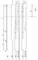
- the sequence of a measuring interval is shown, for example, by the digital control block 4 of the (block) circuit diagram Fig. 1 controlled.
- a measurement activation signal "Measure” (reference numeral 66, Fig. 2 ) at the beginning of the measurement (reference number 67, Fig. 2 ) activated.
- the power sources regulate 27.28 low resistance to the operating point of the receiving diode D.
- the output of the power supply for a compensation diode K is switched to active.
- the compensation diode K already irradiates the photodiode D.
- the compensation diode K is initially not modulated. Due to the low resistance of the current sources 27, 28, the measuring amplifiers 18, 19 quickly reach their operating points.
- the capacitances 20,21 or coupling capacitors 24,25 are charged to their working level.
- the current sources 64, 65, 66, 67 for the operation of three measuring transmitter diodes H1, H2, H3 in this exemplary embodiment (because of the multi-dimensional, in particular 3D gesture recognition) and the compensation diode K are set to the respective operating values.
- phase A At the end of phase A at time 69 ( Fig. 2 ) the signal "hold” (see reference numeral 68, Fig. 2 ) active.
- the voltage-controlled current sources 27, 28 go from their previously assumed low-resistance state to a high-resistance state. This "freezes” your operating points.
- the difference signal 63 of the outputs of the measuring amplifiers 18, 19 should be constant zero, since the operating points are adjusted.
- the modulation signals 45, 46, 47, 48 for the compensation diode K or for the measuring transmitter diodes H1, H2, H3 are square-wave signals which are phase-shifted by 180 ° and which can be regulated in amplitude. (see in measurement phase C Fig. 2 )
- the measurement begins by, for example, weakening or even switching off the radiation from the compensation diode (see reference symbols 45 and 69 in FIG Figs. 1 and 2 ).
- at least one of the transmission signals (see reference numeral 46 and / or 46 and / or 47 in FIG Figs. 1 and 2 ) switched on.
- the typically at least one measuring transmitter diode H1 and / or H2 and / or H3 irradiates the (receiving) photodiode D indirectly via the transmission path to be measured.
- the compensation transmitter diode K and the typically at least one measurement transmitter diode H1 or H2 or H3 are alternately weakened or caused to emit more intensely. Initially, this will lead to a remaining modulation of the output signal of the input stage. After amplification by an amplifier 36, the modulated signal received in this way can be converted into a DC signal with a demodulator. This can be used to regulate the amplitude of the modulation of one measurement transmitter diode or one of the transmitter diodes H1, H2, H3 and / or the amplitude of the modulation of the compensation diode K in each case.
- a regulation of the compensation diode K is shown as case F1 and a regulation of the measurement transmitter diode or diodes H1, H2, H3 as case F2.
- the regulation can be different for the measuring diodes H1, H2 and H3.
- the measurement transmitter diodes H1, H2 and H3 are typically not operated simultaneously but with a time delay. More than one receiving diode can also be used.
- the time offset is typically chosen so that only one receiving diode D and one transmitting diode H1, H2, H3 are active at the same time.
- the measured value obtained in this way readjusts the amplitude of the respective measurement transmitter diode H1, H2, H3. It has been shown that it makes sense to increase this value before the negative feedback. This principle is also known from operational amplifier circuits and is used to suppress parasitic factors and influences.
- DE-B-103 46 741 EP-A-2 546 620 , EP-A-2,356,000 , EP-B-1 410 507 , EP-B-1 435 509 , EP-A-2 418 512 , EP-B-1,269,629 , DE-A-103 22 552 , DE-B-10 2004 025 345 , EP-A-2 405 283 , DE-C-44 11 773 , WO-A-2012/163725 , DE-A-2006 020 579 , DE-B-10 2005 045 993 , EP-B-1 979 764 , DE-A-10 2012 024 778 , DE-A-10 2013 000 376 , DE10 2013 003 791.3 , DEA-10 2013 000 380 , WO-A-2014/096385 , WO-A-2013/124018
- the regulation creates an equilibrium and the output signal 50 of the demodulator 37 represents a measure of the attenuation of the transmission signal in the transmission channel after the amplification mentioned.
- the inventive control of the current sources 27, 28 is noticeable on the input lines 30, 31 in an input resistance to the effect that the current sources are activated depending on typically at least two phases of a measurement cycle (reference symbols A and C, B and C or A and B and C of the Fig. 2 ) fluctuate.
- the effectiveness of the voltage-controlled current sources 27, 28 is limited by the real conditions.
- the current sources 27, 28 can only try to maintain the respectively specified voltage level up to a maximum current.
- the measurement interval (from reference number 67, Fig. 2 , to reference number 71, Fig. 2 ) is ended in that the "Measure" signal (66) at the end of the measuring cycle (see reference numeral 71, Fig. 2 ) becomes inactive again. All transmission signals are switched off and the measurement result is typically frozen in a sample-and-hold circuit (not shown), for example.
- Measurement interval (from reference number 67, Fig. 2 , to reference number 71, Fig. 2 ) to be repeated at shorter or longer intervals.
- Measurement interval from reference number 67, Fig. 2 , to reference number 71, Fig. 2
- higher repetition frequencies for the measurement sequences result in higher power consumption.
- the system can be enabled to provide at least some and typically every measured value with a quality value of the measurement, that is to say to determine the quality of the measurement signal.
- this measure forms an independent subject matter of the invention.
- a sequence of measured values with associated quality values is obtained, which allows a measured value estimator to estimate an optimized measured value and to indicate a probability of the correctness of this measured value.
- the resulting measured value vector can be used, for example, as a basis for the feature extraction of a gesture recognition.
- an interferer does not modulate at a relatively low frequency, such as sunlight, (for example due to shading by trees, for example), but rather quickly, as is the case with fluorescent tubes or when driving in a convertible under trees in the sunshine will.
- a relatively low frequency such as sunlight, (for example due to shading by trees, for example)
- fluorescent tubes or when driving in a convertible under trees in the sunshine will.
- the interference frequency is in the vicinity of the modulation frequency of the measuring transmitter diodes H1, H2, H3 and of the compensation transmitter K, this frequency is usually not hit correctly.
- There is a beating in the control signal which can be recognized and used.
- the quality of the measurement will typically fluctuate with the beat frequency as a function of time.
- the system since, as a result of the evaluation of the measurement results, the system only evaluates measurement value sequences that are relatively undisturbed, the measurement signal is de facto automatically sampled only at times that are relatively undisturbed.
- the measurement signal is de facto automatically sampled only at times that are relatively undisturbed.
- an estimator determines a high probability of disturbance. This can for example be directly preceding or directly following measured values.
- Such a measuring system should also initiate countermeasures when faults are detected.
- the circuit can also be parameterized differently. For example, the time constants of the measuring amplifiers 18, 19 acting as integrators can be changed in that the capacitances 20, 21 can be changed. In the extreme case, the integrators can be bridged by bridging their capacitances 20, 21 with the aid of the programmable switches 22, 23. As you can see from this example, a change in the system or circuit topology is also an option. The integrators then become pure impedance converters.
- a further improvement of the device can therefore be achieved by assessing the quality of the measurement signal and / or by regulating to optimize the measurement results.
- the feedback loop is closed by software, since the control algorithms are very application-dependent.
- a change in the system parameters and / or the system topology or structure is typically used as an actuator for this measurement signal quality control.
- the current supplied by the current source or current sources 27, 28 is measured as a function of time in block 16 (“extrinsic light measurement” or “measurement of the external light”).
- exa Fourier transformation can be used to determine the interference frequencies that interfere with the measurement signal. It is particularly advantageous to adjust the modulation frequency of the measuring transmitter diodes H1, H2, H3 and the Compensation diode K and the repetition frequency of the measuring intervals (reference numeral 67, Fig. 2 , to reference number 71, Fig. 2 ) to be selected in such a way that they do not interfere with the interference frequencies as far as possible.
- the interference signal robustness can be increased by "frequency hopping".
- Such possible transmission signals are, for example, suitable pseudo-random sequences (see also EP-A-2 631 674 , the content of which is hereby the subject of the present application by reference)
- Another measure representing an independent inventive concept is the introduction and / or raising of a threshold for the detection of the approach of an object to the measuring transmitter diodes H1, H2, H3 / receiving diode D.
- This is a non-linear filter function, which is typically in block 37 the Fig. 1 is realized, but can also be realized in a subsequent processing stage. All measured values below or above a threshold are fixed, for example, to a predefined value.
- a computational model of an interferer can be parameterized and points in time and setting parameters for the measuring system can be predicted with which the next measuring interval can be carried out with particularly good quality.
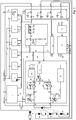
- the circuit according to Fig. 1 has such an interface 53 (see in Fig. 1 top right), which is provided with a corresponding input hardware 7.
- the interface has, for example, a serial TX and RX two-wire line or an I 2 C bus interface 54, an interrupt output 55 for the main processor, which must be at a defined potential, a non-maskable measuring system reset 56 and a reference voltage input 57. All other systems are switched off. If possible, the normal system oscillator 6 is also switched off and instead this function block 14 of the circuit with a low frequency from a minimum oscillator 5 supplied. This is much smaller because it doesn't have to drive the entire IC.
- band gap reference 2 the block 4 (digital control), the voltage regulator 1 and all measuring amplifiers and receiving and transmitting devices are switched off.
- the interface 54 is, for example, an I 2 C interface, it makes sense to design the function block 14 so that it can only recognize a very specific command on the bus that is sent to a precisely specified register address.
- Such a protocol can for example be such that the function block 14 recognizes a sequence of a start bit and the slave address and a bit for signaling a write access and then outputs an acknowledge bit, whereupon the main processor sends the register address, the function block 14 sends an acknowledge bit and the main processor then sends a parity bit. If the function block 14 has recognized all of these data as correct, the voltage regulator, the bandgap reference 2 and all other parts of the circuit are started up in a predefined sequence one after the other and / or in parallel, depending on the type and requirement. The normal I 2 C bus communication is then taken over again by block 4 (digital control) until the next sleep command.
- block 4 (digital control) causes the essential parts of the measuring system to switch to energy-saving mode.
- the last part of the shutdown sequence must be controlled by function block 14. This applies in particular to the switching off of the energy supply by switching off the voltage regulator 1, the oscillator 6 and the block 4 (digital control) itself.
- the function block 14 has an internal timer that can wake up the system at regular intervals, without the need to receive a command from the main processor via the interface 54 for this purpose.
- the measured values and preferably also the measured value qualities are stored in a memory (not shown).
- the measured values stored there can also include configuration data of the system (for example with which of the transmitting diodes H1, H2, H3, with which of the compensation diode K and with which receiving diode D, when and with what quality measured values were recorded for example of block 16 (Extrinsic Light Measurement).
- the bandgap reference 2 which only supplies a reference voltage for use at different points in the measuring system, can be temporarily switched off if its voltage is temporarily stored and buffered in a sample-and-hold circuit, for example.
- the bandgap circuit is then only switched on from time to time to renew the inevitably slowly draining charges from the storage element of the sample-and-hold circuit (typically a capacitor).
- Another independently essential feature of the device results from the necessary calibration of the measuring system.
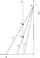
- Fig. 3 the control characteristics of the system with control of the transmitter diode amplitude T i are shown.
- the amplitude of the portion to be traced back to the respective measuring transmitter diode H1, H2, H3 (see 72,75,77 in Fig. 3 ) of The photocurrent I PD in the / a receiving diode D depends on the transmitting diode amplitude T i .
- the amplitude of the component to be traced back to the compensation diode K or the respective compensation diode K (see line 73 in Fig. 3 ) of the photocurrent I PD in the / a receiving diode D does not depend on the transmitter amplitude T i.
- the difference signal 63 is a constant signal.
- the portion to be traced back to the transmission signal is then zero in the difference signal 63.
- the maximum distance from which an object approaching the receiving diode or up to which an object moving away from the receiving diode can still be recognized is determined by the control characteristic and / or the fact that at the maximum amplitude of the transmitting diode signal from the object there is still a so large a portion of the transmitting diode signal is reflected that a signal with at least the amplitude of the compensation diode signal is received at the receiving diode.
- a large photocurrent 72 which is synonymous with a nearby object (and thus for a steep control characteristic)
- there is a first working point 74 as an intersection with 73.
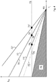
- the offset signal does not lead to one more achievable area 79 in the diagram of Fig. 4 .
- the generation of this offset signal is in Fig. 1 indicated by a calibration block 81 which generates the offset signal 82 for the respective transmitter / receiver combination from the transmitter signals 9 to 12, from which the signal 82 is generated by addition.
- the overall system differs from the measuring system, for example, in that, in addition to the measuring system, it also includes optical elements such as mirrors, diaphragms, etc. and of course the housing.
- the compensation diode K is switched to a static level.
- the coupling between receiving diode D and compensation diode K can only be stabilized with great difficulty. Therefore, the coupling is always to be assumed to be the same for one application type, but to vary from application to application within the same type.
- the calibration now takes place in such a way that the switchable reference current sources 41, 42, 43 are provided, with which the reference current supply 38 is now set so that the measured photocurrent is always set to the same, application-specific predetermined value.
- This allows the ordinate position of the line 73 in the Figs. 3 and 4th can be specified. This ensures that an operating point is found.
- This operating point is typically set in such a way that the compensation transmitting diode current is increased until the compensation signal can be measured above the system noise.
- the offset signal is then set to such a value that the lowest operating point is assumed.
Description
Die Erfindung betrifft eine störstrahlungskompensierte Vorrichtung zur Vermessung einer optischen Signalübertragungsstrecke während einer Vielzahl von insbesondere intermittierend aufeinanderfolgenden Messintervallen insbesondere für die Erkennung eines Objekts und/oder für die Erkennung einer Bewegung und/oder Bewegungsvorrichtung eines Objekts.The invention relates to a radiation-compensated device for measuring an optical signal transmission path during a plurality of, in particular, intermittently successive measuring intervals, in particular for the detection of an object and / or for the detection of a movement and / or movement device of an object.
Aus dem Stand der Technik sind verschiedene Verfahren zur Vermessung optischer Strecken bekannt.Various methods for measuring optical paths are known from the prior art.
Hierbei wird typischerweise eine Fotodiode in Sperrrichtung betrieben. Es hat sich als besonders vorteilhaft erwiesen, die Fotodiode zur Kompensation eines aus (z.B. Umgebungs-)Störstrahlung resultierenden Fotostroms durch eine spannungsgesteuerte Stromquelle zu bestromen und in einem spannungsmäßig vorbestimmten Arbeitspunkt zu halten.In this case, a photodiode is typically operated in the reverse direction. It has proven to be particularly advantageous to energize the photodiode to compensate for a photocurrent resulting from (e.g. ambient) interference radiation by a voltage-controlled current source and to keep it at a voltage-related predetermined operating point.
Eine besonders vorteilhafte Anordnung zur Vermessung einer optischen Übertragungsstrecke oder zur Vermessung eines Objekts, das sich innerhalb einer solchen Übertragungsstrecke befindet, ist die Vermessung mit Hilfe einer Kompensationsmethode, wie sie z.B. unter dem Namen HALIOS® bekannt ist. Hierbei strahlen ein Kompensationssender und ein Sender gleichzeitig überlagernd in einen Empfänger ein. Das Signal des Kompensationssenders ist dabei zeitlich komplementär, d.h. um 180° phasenverschoben zu demjenigen des Senders gewählt. Das bedeutet, dass sich beide Signale bei gleicher Einstrahlamplitude in dem Empfängersignal zu einem Gleichsignal überlagern.A particularly advantageous arrangement for measuring an optical transmission path or for measuring an object that is located within such a transmission path is measurement with the help of a compensation method such as is known, for example, under the name HALIOS®. Here, a compensation transmitter and a transmitter simultaneously radiate superimposed into a receiver. The signal from the compensation transmitter is complementary in time, i.e. it is selected to be 180 ° out of phase with that of the transmitter. This means that, given the same beam amplitude, the two signals are superimposed in the receiver signal to form a constant signal.
Eine Regelung erzeugt aus dem Empfangssignal ein Regelsignal. Mit diesem Regelsignal wird nun entweder der Sender oder der Kompensationssender oder auch nach einem festen Regelschema beide Sender geregelt.A control generates a control signal from the received signal. With this control signal, either the transmitter or the compensation transmitter or both transmitters are controlled according to a fixed control scheme.
Bei richtiger Vorzeichenwahl der Verstärkung des Reglers werden parasitäre Einflüsse eliminiert. Dies betrifft vor allem Verschmutzungen und Drift des Empfängers.If the correct sign of the controller gain is selected, parasitic influences are eliminated. This mainly affects soiling and drift of the receiver.
Vorrichtungen der zuvor genannten Art sind beispielhaft
Es hat sich gezeigt, dass die Verwendung von spannungsgesteuerten Stromquellen zur Einstellung eines Kompensations- bzw. Bias-Stromes für als Empfänger verwendete Fotodioden besonders vorteilhaft ist. Dies ist beispielsweise bereits in
Ein wesentlicher Nachteil einer Arbeitspunkteinstellung der obigen Art mit Hilfe eines Gyrators ist der niedrige Eingangswiderstand des Gyrators, der das Ausgangssignal der Fotodiode belastet und dämpft.A major disadvantage of setting the operating point of the above type with the aid of a gyrator is the low input resistance of the gyrator, which loads and attenuates the output signal of the photodiode.
Dies führt zu einer Reduktion der Empfindlichkeit. Soll ein derartiges System zur Erkennung dreidimensionaler Gesten eingesetzt werden, so wird die Reichweite des Systems herabgesetzt.This leads to a reduction in sensitivity. If such a system is to be used to recognize three-dimensional gestures, the range of the system is reduced.
Auf der anderen Seite kann die Empfindlichkeit für das Messsignal erhöht werden. Dies geschieht jedoch zu Lasten der Störempfindlichkeit. Es ist ein bekanntes Problem, dass beispielsweise optische Gestenerkennungssysteme durch Leuchtstoffröhren gestört werden können.On the other hand, the sensitivity for the measurement signal can be increased. However, this is done at the expense of susceptibility to interference. It is a known problem that, for example, optical gesture recognition systems can be disrupted by fluorescent tubes.
Insbesondere für mobile Anwendungen ist es besonders von Vorteil, wenn der Energieverbrauch möglichst gering ist.For mobile applications in particular, it is particularly advantageous if the energy consumption is as low as possible.
Es ist daher die Aufgabe der Erfindung, eine störstrahlungskompensierte Vorrichtung mit der Möglichkeit der Reduktion des Energieverbrauchs zu schaffen.It is therefore the object of the invention to create a radiation-compensated device with the possibility of reducing energy consumption.
Zur Lösung dieser Aufgabe wird mit der Erfindung eine störstrahlungskompensierte Vorrichtung zur Vermessung einer optischen Signalübertragungsstrecke während einer Vielzahl von insbesondere intermittierend aufeinanderfolgenden Messintervallen insbesondere für die Erkennung eines Objekts und/oder für die Erkennung einer Bewegung und/oder Bewegungsvorrichtung eines Objekts vorgeschlagen, mit
- mindestens einem Messsender zum Senden eines optischen Messsignals,
- mindestens einem Empfänger zum Empfangen eines optischen Signals, wobei der mindestens eine Empfänger einer Störstrahlung z.B. aus der Umgebung ausgesetzt ist,
- einer Ansteuer- und Auswerteeinheit zur Ansteuerung des mindestens einen Messsenders und des mindestens einen Empfängers zwecks Sendens bzw. Empfangens eines optischen Signals während einer Messphase eines Messintervalls und zur Auswertung des empfangenen optischen Messsignals durch Verarbeitung eines elektrischen Signals, das an einem ersten elektrisch mit dem mindestens einen Empfänger gekoppelten Schaltungsknoten ansteht und mittels eines Messverstärkers (18, 19) verstärkt ist, und
- mindestens einer mit dem ersten Schaltungsknoten gekoppelten ersten Störstrahlungs-Kompensationseinheit zur elektrischen Vorspannung des mindestens einen Empfängers durch Bereitstellen eines ersten Kompensationsstroms mit einer Größe, die im Wesentlichen gleich der Größe eines in Folge der Störstrahlung von dem mindestens einen Empfänger erzeugten Störsignals ist, und
- einer Funktionseinheit zur Überführung des mindestens einen Messsenders und der mindestens einen ersten Störstrahlungs-Kompensationseinheit in einen Stromsparmodus, in dem lediglich die Funktionseinheit (14) und ein Systemoszillator (6) aktiv sind und in dem der mindestens eine Messsender und die mindestens eine erste Störstrahlungs-Kompensationseinheit abgeschaltet sind.
- at least one measuring transmitter for sending an optical measuring signal,
- at least one receiver for receiving an optical signal, the at least one receiver being exposed to interference radiation, for example from the environment,
- a control and evaluation unit for controlling the at least one measuring transmitter and the at least one receiver for the purpose of sending or receiving an optical signal during a measuring phase of a measuring interval and for evaluating the received optical measuring signal by processing an electrical signal that is electrically connected to the at least at a first a receiver-coupled circuit node is present and is amplified by means of a measuring amplifier (18, 19), and
- at least one first interference radiation compensation unit coupled to the first circuit node for electrical biasing of the at least one receiver by providing a first compensation current with a magnitude that is substantially equal to the magnitude of an interference signal generated as a result of the interference radiation from the at least one receiver, and
- a functional unit for converting the at least one measuring transmitter and the at least one first interference radiation compensation unit into a power-saving mode in which only the functional unit (14) and a system oscillator (6) are active and in which the at least one measuring transmitter and the at least one first interference radiation Compensation unit are switched off.
In vorteilhafter Weiterbildung der Erfindung kann vorgesehen sein, dass der mindestens eine Empfänger zwischen dem ersten Schaltungsknoten und einem zweiten Schaltungsknoten, mit denen er jeweils elektrisch gekoppelt ist, geschaltet ist, wobei die mindestens eine erste Störstrahlungs-Kompensationseinheit mit dem ersten Schaltungsknoten gekoppelt ist, dass die an und/oder zwischen diesen Schaltungsknoten anstehenden elektrischen Signale der Ansteuer- und Auswerteinheit zuführbar sind und dass mindestens eine zweite Störstrahlungs-Kompensationseinheit mit variablem Innenwiderstand vorhanden ist, die einen zweiten Kompensationsstrom bereitstellt, welcher im Wesentlichen gleich dem ersten Kompensationsstrom ist, und dass die Funktionseinheit (14) im Stromsparmodus auch die zweite Störstrahlungs-Kompensationseinheit (28,29) abschaltet.In an advantageous development of the invention it can be provided that the at least one receiver between the first circuit node and a second circuit node, to which it is electrically coupled, is connected, wherein the at least one first interference radiation compensation unit is coupled to the first circuit node, that the electrical signals pending at and / or between these circuit nodes can be fed to the control and evaluation unit and that at least one second radiation compensation unit with variable internal resistance is present, which provides a second compensation current which is essentially equal to the first compensation current, and that the functional unit (14) also switches off the second interference radiation compensation unit (28, 29) in power-saving mode.
Vorzugsweise ist vorgesehen, dass die Funktionseinheit an einen Bus angeschlossen ist und zur Umschaltung von dem Normalbetrieb in den Stromsparmodus und umgekehrt einen an eine vorgegebene Registeradresse gesendeten Befehl auf dem Bus erkennt.It is preferably provided that the functional unit is connected to a bus and, in order to switch from normal operation to power-saving mode and vice versa, recognizes a command sent to a predetermined register address on the bus.
In vorteilhafter Ausgestaltung der Erfindung kann vorgesehen sein, dass die Funktionseinheit einen internen Zeitgeber aufweist, der die Vorrichtung in regelmäßigen Zeitabständen aufweckt.In an advantageous embodiment of the invention, it can be provided that the functional unit has an internal timer which wakes up the device at regular time intervals.
Weitere Ausgestaltungen der Erfindung können eines oder mehrere der nachfolgend genannten Merkmale aufweisen:
- durch eine Ablaufsteuerung zur Ansteuerung der Funktionseinheit zur Überführung aus dem Normalbetrieb in den Stromsparmodus, und zwar nach Durchführung vorgebbarer und/oder einstellbarer Aufgaben und/oder Messaufgaben,
- mindestens eine Band-Gap-Referenz, die durch eine Ablaufsteuerung lediglich zeitweise aktivierbar ist und deren analoge Ausgangswerte insbesondere in einer Sample-And-Hold-Schaltung zwischenspeicherbar sind,
- mindestens eine Band-Gap-Referenz, die durch eine Ablaufsteuerung lediglich zeitweise aktivierbar ist und deren analoge Ausgangswerte insbesondere in einer Sample-And-Hold-Schaltung während eines durch die Funktionseinheit gesteuerten aktivierten Stromsparmodus der Band-Gap-Referenz zwischengespeichert werden,
- mindestens eine Band-Gap-Referenz, die in einem durch die Funktionseinheit ausgelösten Stromsparmodus abgeschaltet ist
- mindestens einen Spannungsregler zur Versorgung von zumindest Teilen der Vorrichtung mit elektrischer Energie, wobei der Spannungsregler, gesteuert durch die Funktionseinheit, in einem Stromsparmodus abgeschaltet ist,
- eine lediglich zeitweise Aktivierung mittels eines Band-Gap externes Signal und eine Zwischenspeicherung von analogen Ausgangswerten in insbesondere einer Sample-And-Hold-Schaltung während des durch die Funktionseinheit aktivierten Stromsparmodus für eine Band-Gap-Referenz, wobei der Stromsparmodus durch ein Band-Gap externes Signal gesteuert abschaltbar ist.
- by a sequence control for controlling the functional unit for transferring from normal operation to power-saving mode, namely after performing predefinable and / or adjustable tasks and / or measurement tasks,
- at least one band gap reference, which can only be activated temporarily by a sequence control and whose analog output values can be temporarily stored, in particular in a sample-and-hold circuit,
- at least one band gap reference which can only be activated temporarily by a sequence control and whose analog output values in particular in a sample-and-hold circuit during a through Functional unit-controlled, activated power-saving mode of the band-gap reference are temporarily stored,
- at least one band gap reference that is switched off in a power-saving mode triggered by the functional unit
- at least one voltage regulator for supplying at least parts of the device with electrical energy, wherein the voltage regulator, controlled by the functional unit, is switched off in a power-saving mode,
- an only temporary activation by means of a band gap external signal and an intermediate storage of analog output values in particular in a sample-and-hold circuit during the power-saving mode activated by the functional unit for a band-gap reference, the power-saving mode being a band-gap external signal can be switched off in a controlled manner.
Die Erfindung lässt sich insbesondere einsetzen bei einer störstrahlungskompensierten Vorrichtung zur Vermessung einer optischen Signalübertragungsstrecke während einer Vielzahl von insbesondere intermittierend aufeinanderfolgenden Messintervallen insbesondere für die Erkennung eines Objekts und/oder für die Erkennung einer Bewegung und/oder Bewegungsvorrichtung eines Objekts vorgeschlagen, mit
- mindestens einem Messsender zum Senden eines optischen Messsignals,
- mindestens einem Empfänger zum Empfangen eines optischen Signals, wobei der mindestens eine Empfänger einer Störstrahlung z.B. aus der Umgebung ausgesetzt ist,
- einer Ansteuer- und Auswerteeinheit zur Ansteuerung des mindestens einen Messsenders und des mindestens einen Empfängers zwecks Sendens bzw. Empfangens eines optischen Signals während einer Messphase eines Messintervalls und zur Auswertung des empfangenen optischen Messsignals durch Verarbeitung eines elektrischen Signals, das an einem ersten elektrisch mit dem mindestens einen Empfänger gekoppelten Schaltungsknoten ansteht,
- mindestens einer mit dem ersten Schaltungsknoten gekoppelten ersten Störstrahlungs-Kompensationseinheit zur elektrischen Vorspannung des mindestens einen Empfängers durch Bereitstellen eines ersten Kompensationsstroms mit einer Größe, die im Wesentlichen gleich der Größe eines in Folge der Störstrahlung von dem mindestens einen Empfänger erzeugten Störsignals ist,
- wobei die mindestens eine erste Störstrahlungs-Kompensationseinheit einen variablen Innenwiderstand aufweist und
- wobei die Ansteuer- und Auswerteeinheit den Innenwiderstand der mindestens einen ersten Störstrahlungs-Kompensationseinheit während einer ersten Vorbereitungsphase vor der Messphase eines Messintervalls auf einen niedrigeren ersten Widerstandswert und während der Messphase auf einen höheren zweiten Widerstandswert einstellt.
- at least one measuring transmitter for sending an optical measuring signal,
- at least one receiver for receiving an optical signal, the at least one receiver being exposed to interference radiation, for example from the environment,
- a control and evaluation unit for controlling the at least a measuring transmitter and the at least one receiver for the purpose of sending or receiving an optical signal during a measuring phase of a measuring interval and for evaluating the received optical measuring signal by processing an electrical signal that is present at a first circuit node electrically coupled to the at least one receiver,
- at least one first interference radiation compensation unit coupled to the first circuit node for electrical biasing of the at least one receiver by providing a first compensation current with a magnitude that is essentially equal to the magnitude of an interference signal generated by the interference radiation from the at least one receiver,
- wherein the at least one first interference radiation compensation unit has a variable internal resistance and
- wherein the control and evaluation unit sets the internal resistance of the at least one first interference radiation compensation unit during a first preparation phase before the measurement phase of a measurement interval to a lower first resistance value and during the measurement phase to a higher second resistance value.
Ausgangspunkt für die Überlegungen, die zu dieser Weiterbildung der Erfindung geführt haben, ist eine reduzierte Strom- bzw. Energieaufnahme einer störstrahlungskompensierten Vorrichtung zur Vermessung einer optischen Signalübertragungsstrecke. Die reduzierte Stromaufnahme ist insbesondere vorteilhaft beim Einsatz einer solchen Vorrichtung in mobilen Geräten, die lediglich über begrenzte Energieressourcen verfügen.The starting point for the considerations that led to this development of the invention is a reduced current or energy consumption of a radiation-compensated device for measuring an optical signal transmission path. The reduced power consumption is particularly advantageous when using such a device in mobile devices that only have limited energy resources.
Wenn optische Signalübertragungsstrecken vermessen werden, um beispielsweise die Annäherung eines Objekts, eine Verschmutzung o.dgl. erkennen zu können, besteht stets das Problem darin, dass derartige Signalübertragungsstrecken durch Umgebungslicht "gestört" werden. Dabei stellt sich die weitere Schwierigkeit dahingehend dar, dass die Störsignale weitaus größer sind als die Nutzsignale. Würde man also die Störung vorab nicht kompensieren, bestünde die Gefahr, das Nutzsignal innerhalb des Störsignals nicht so ohne Weiteres erkennen zu können. Man könnte sicherlich mit kodierten Nutzsignalen arbeiten, um dann durch Autokorrelation o.dgl. Korrelationsverfahren das Nutzsignal aus dem Gesamtsignal extrahieren zu können. Derartige auch unter dem Begriff Spreizcode-Verfahren bekannte Systeme sind aber in ihrer Umsetzung recht aufwändig.If optical signal transmission routes are measured, for example, to the approach of an object, pollution or the like. To be able to recognize, there is always the problem that such signal transmission paths are "disturbed" by ambient light. Another difficulty is that the interfering signals are much larger than the useful signals. If one were not to compensate for the disturbance in advance, it would exist the risk of not being able to easily recognize the useful signal within the interfering signal. One could certainly work with coded useful signals in order to then use autocorrelation or the like. Correlation method to extract the useful signal from the total signal. Such systems, also known under the term spreading code method, are, however, very complex to implement.
Zur Störstrahlungskompensation optischer Empfänger von Vorrichtungen zur Vermessung optischer Signalübertragungsstrecken werden Störstrahlungs-Kompensationseinheiten eingesetzt, die einen Strom erzeugen, der im Wesentlichen gleich demjenigen Strom ist, der im Empfänger in Folge des Empfangs von Umgebungslicht o.dgl. Störlicht entsteht. Wird dann ein derartig störkompensierter Empfänger mit einem Nutz- bzw. optischen Messsignal beaufschlagt, wie es für die Vermessung der optischen Signalübertragungsstrecke erforderlich ist, so wird in der Ansteuer- und Auswerteeinheit anschließend auch nur noch dieses empfangene Messsignal ausgewertet.For interference radiation compensation of optical receivers of devices for measuring optical signal transmission paths, interference radiation compensation units are used which generate a current which is essentially the same as that which is generated in the receiver as a result of the reception of ambient light or the like. Stray light arises. If such an interference-compensated receiver is then subjected to a useful or optical measurement signal, as is necessary for measuring the optical signal transmission path, then only this received measurement signal is then evaluated in the control and evaluation unit.
Die Störstrahlungskompensation sollte recht stabil sein, damit die Vorrichtung zuverlässige Auswertungen und Vermessungen der optischen Signalübertragungsstrecke liefert. Dies ist grundsätzlich kein Problem bei dauerhaft aktivierten Vorrichtungen, also bei Vorrichtungen, die im Grunde genommen ständig messbereit sind. Da eine solche Vorgehensweise aber auch während der Zeiträume, in denen nicht zwingend gemessen werden muss, Energie benötigt, eignet sich eine solche Vorgehensweise bei mobilen Endgeräten mit begrenzten Energieressourcen nicht. Daher wird bei der Erfindung dazu übergegangen, die Vorrichtung lediglich für einzelne Messintervalle messbereit zu halten. In den Zeiträumen zwischen den Messintervallen benötigt die Vorrichtung dann lediglich eine vergleichsweise geringe Stromaufnahme.The interference radiation compensation should be quite stable so that the device delivers reliable evaluations and measurements of the optical signal transmission path. In principle, this is not a problem with permanently activated devices, i.e. with devices that are basically always ready to measure. However, since such a procedure also requires energy during the periods in which it is not absolutely necessary to measure, such a procedure is not suitable for mobile terminals with limited energy resources. The invention therefore moves on to keeping the device ready for measurement only for individual measurement intervals. In the time periods between the measurement intervals, the device then only requires a comparatively low power consumption.
Die Störstrahlungs-Kompensationseinheit ist wie die Ansteuer- und Auswerteeinheit elektrisch mit dem Empfänger gekoppelt. Damit nun ein vom Empfänger empfangenes Nutzsignal zu nahezu 100 % von der Ansteuer- und Auswerteeinheit auch empfangen werden kann, sollte die Störstrahlungs-Kompensationseinheit relativ hochohmig ausgeführt sein, so dass das am Ausgang des Empfängers anstehende elektrische Signal nur zu einem sehr geringen Anteil zur Störstrahlungs-Kompensationseinheit "abfließt" und damit in ganz überwiegendem Maße der Ansteuer- und Auswerteeinheit zugeführt werden kann. Eine hochohmige Störstrahlungs-Kompensationseinheit, also eine Störstrahlungs-Kompensationseinheit mit hohem Innenwiderstand ist aber insoweit nachteilig, als sie die Arbeitspunkteinstellung im Vorfeld der Bereitschaltung der Vorrichtung für den Empfang von Nutzsignalen verlangsamt. Während dieser Phase des Betriebs der Vorrichtung ist es nämlich wünschenswert, wenn die Störstrahlungs-Kompensationseinheit einen geringen Innenwiderstand aufweist.The radiated interference compensation unit, like the control and evaluation unit, is electrically coupled to the receiver. So that a useful signal received by the receiver can now also be received by the control and evaluation unit to almost 100%, the interference radiation compensation unit should be designed to be relatively high resistance, so that the electrical signal present at the output of the receiver only "flows away" to the interference radiation compensation unit to a very small extent and can thus be fed to the control and evaluation unit to a very large extent. A high-resistance radiated interference compensation unit, that is to say a radiated interference compensation unit with high internal resistance, is disadvantageous insofar as it slows down the setting of the operating point before the device is made ready for the reception of useful signals. This is because it is desirable during this phase of the operation of the device if the interference radiation compensation unit has a low internal resistance.
Erfindungsgemäß wird also nun der Innenwiderstand der Störstrahlungs-Kompensationseinheit in einer Vorbereitungsphase, die vor der eigentlichen Messphase eines Messintervalls liegt, auf einen niedrigen ersten Widerstandswert eingestellt, während der Innenwiderstand für die Dauer der Messphase auf einen höheren zweiten Widerstandswert gesteuert wird. Mit "variablem" Widerstand ist im Sinne der Erfindung gemeint, dass der Widerstand einen von mehr als zwei unterschiedlichen Werten (Impedanz, ohmsch, kapazitiv und/oder induktiv) annehmen kann, wobei die Widerstandswerte vorzugsweise jeweils ungleich Null und/oder ungleich Unendlich sind. Mit "variabel" ist also insbesondere nicht der Falle ines festen Vor- oder Innenwiderstands gemeint, der je nach Bedarf aufgeschaltet oder überbrückt also "aktiviert" oder "deaktiviert" wird.According to the invention, the internal resistance of the interference radiation compensation unit is now set to a low first resistance value in a preparation phase, which occurs before the actual measurement phase of a measurement interval, while the internal resistance is controlled to a higher second resistance value for the duration of the measurement phase. In the context of the invention, "variable" resistance means that the resistance can assume one of more than two different values (impedance, ohmic, capacitive and / or inductive), the resistance values preferably being unequal to zero and / or unequal to infinity. The term “variable” does not mean, in particular, the case of a fixed series or internal resistance that is switched on or bridged, ie “activated” or “deactivated”, as required.
Bei der zuvor beschriebenen Variante der Erfindung ist der Empfänger zwischen Masse und einem Arbeitspotential geschaltet, das durch die Störstrahlungs-Kompensationseinheit definiert ist. Es ist darüber hinaus möglich und von der Erfindung umfasst, dass der Empfänger zwischen zwei Schaltungsknoten geschaltet ist, wobei jeder dieser Schaltungsknoten mit einer Störstrahlungs-Kompensationseinheit verbunden/gekoppelt ist, die Vorrichtung also zwei Störstrahlungs-Kompensationseinheiten aufweist. Das Nutzsignal wird dabei zwischen diesen beiden Schaltungsknoten abgegriffen und in der Ansteuer- und Auswerteeinheit verarbeitet. Eine derartige Zweikanal-Ausführung der Vorrichtung weist eine verbesserte Robustheit gegenüber elektrischen und/oder magnetischen Fernfeldstörungen auf. Der Gedanke dabei ist es, zwei geometrisch und/oder elektrisch im wesentlichen identische Messkanäle vorzusehen, die Fernfeldstörungen im wesentlichen im gleichen Maße ausgesetzt sind, um die durch Fernfeldstörungen erzeugten Störsignale in einem nachgeschalteten (Haupt-)Differenzbildner zu eliminieren. Sofern die beiden Sensorelemente und/oder Messkanäle eine bekannte Ungleichheit (auch Asymmetrie genannt) aufweisen, kann diese durch eine (ggf. einstellbare) Gewichtung im Differenzbildner ausgeglichen werden, was insbesondere im Hinblick auf eine hohe Unterdrückung von elektromagnetischem Rauschen erfolgt.In the variant of the invention described above, the receiver is connected between ground and a working potential which is defined by the interference radiation compensation unit. It is furthermore possible and encompassed by the invention that the receiver is connected between two circuit nodes, each of these circuit nodes being connected / coupled to an interference radiation compensation unit, that is to say the device has two interference radiation compensation units. The useful signal is tapped between these two circuit nodes and in the Control and evaluation unit processed. Such a two-channel design of the device has improved robustness against electrical and / or magnetic far-field interference. The idea here is to provide two geometrically and / or electrically essentially identical measuring channels that are exposed to far-field interference to the same extent, in order to eliminate the interference signals generated by far-field interference in a downstream (main) subtractor. If the two sensor elements and / or measurement channels have a known inequality (also called asymmetry), this can be compensated for by weighting (possibly adjustable) in the difference calculator, which is done in particular with regard to a high level of suppression of electromagnetic noise.
Insoweit ist es also zweckmäßig, wenn der mindestens eine Empfänger zwischen einem ersten und einem zweiten Schaltungsknoten, mit denen er jeweils elektrisch gekoppelt ist, geschaltet ist, wobei die mindestens eine erste Störstrahlungs-Kompensationseinheit mit dem ersten Schaltungsknoten gekoppelt ist, wobei die an und/oder zwischen diesen Schaltungsknoten anstehenden elektrischen Signale der Ansteuer- und Auswerteinheit zuführbar sind und wobei mindestens eine zweite Störstrahlungs-Kompensationseinheit mit variablem Innenwiderstand vorhanden ist, die einen zweiten Kompensationsstrom bereitstellt, welcher im Wesentlichen gleich dem ersten Kompensationsstrom ist, und wobei die Ansteuer- und Auswerteeinheit den Innenwiderstand der zweiten Störstrahlungs-Kompensationseinheit während eines Messintervalls in im Wesentlichen gleicher Weise wie den Innenwiderstand der ersten Störstrahlungs-Kompensationseinheit steuert. Diese Verschaltung des Empfängers mit zwei Schaltungsknoten führt zu einer Gleichtaktunterdrückung von Störstrahlungen.In this respect it is expedient if the at least one receiver is connected between a first and a second circuit node to which it is electrically coupled, the at least one first interference radiation compensation unit being coupled to the first circuit node, the to and / or electrical signals pending between these circuit nodes can be fed to the control and evaluation unit and at least one second interference radiation compensation unit with variable internal resistance is present, which provides a second compensation current which is essentially equal to the first compensation current, and wherein the control and evaluation unit controls the internal resistance of the second interference radiation compensation unit during a measurement interval in essentially the same way as the internal resistance of the first interference radiation compensation unit. This interconnection of the receiver with two circuit nodes leads to common-mode rejection of interference radiation.
Zur weiteren Kompensation von auf die Vorrichtung einwirkenden Störeinflüssen ist es zweckmäßig, wenn der Empfänger wechselweise optische Signale empfängt, die alternierend von dem Messsender und von einem Kompensationssender ausgesendet werden. Der Kompensationssender strahlt dabei direkt in den Empfänger ein, während der Messsender in die Übertragungsstrecke strahlt, wobei das Messsignal bei Vorhandensein eines Objekts zum Empfänger teilweise reflektiert wird. Dieses Konzept entspricht dem Messsystem gemäß HALIOS®.In order to further compensate for interfering influences acting on the device, it is expedient if the receiver alternately receives optical signals which are transmitted alternately by the measuring transmitter and by a compensation transmitter. The compensation transmitter shines directly into the receiver, while the measurement transmitter radiates into the transmission path, the measurement signal being partially reflected to the receiver if an object is present. This concept corresponds to the measuring system according to HALIOS®.
Bei einem derartigen Konzept kann in vorteilhafter Weise vorgesehen sein, dass die Ansteuer- und Auswerteeinheit den mindestens einen Kompensationssender zwecks Sendens des optischen Kompensationssignals während einer sich an die erste Vorbereitungsphase anschließenden und der Messphase vorgelagerten zweiten Vorbereitungsphase eines Messintervalls ansteuert und dass die Ansteuer- und Auswerteeinheit den Innenwiderstand der mindestens einen ersten Störstrahlungs-Kompensationseinheit und, sofern vorhanden, der mindestens einen zweiten Störstrahlungs-Kompensationseinheit für die Dauer der zweiten Vorbereitungsphase eines Messintervalls auf einen Widerstandswert einstellt, der gleich dem ersten und/oder zweiten Widerstandswert oder zwischen diesen liegt und größer ist als während des Messintervalls sowie größer ist als außerhalb der zweiten Vorbereitungsphase. In dieser zweiten Vorbereitungsphase sendet der Kompensationssender vorzugsweise kontinuierlich, so dass sich die Störstrahlungs-Kompensationseinheit bzw. -einheiten arbeitspunktmäßig auf diese Situation einstellen kann/können. Auch in dieser zweiten Vorbereitungsphase, die zwischen der ersten Vorbereitungsphase und der Messphase eines Messintervalls liegt, weist die bzw. jede Störstrahlungs-Kompensationseinheit einen Innenwiderstandswert auf, der kleiner ist als während der Messphase; die Störstrahlungs-Kompensationseinheit bzw. -einheiten reagieren also wiederum relativ schnell, wobei es dabei bleibt, dass sie hochohmig geschaltet sind, wenn die eigentliche Messung in der Messphase erfolgt.In such a concept, it can advantageously be provided that the control and evaluation unit controls the at least one compensation transmitter for the purpose of sending the optical compensation signal during a second preparation phase of a measurement interval that follows the first preparation phase and precedes the measurement phase, and that the control and evaluation unit sets the internal resistance of the at least one first interference radiation compensation unit and, if present, the at least one second interference radiation compensation unit for the duration of the second preparation phase of a measurement interval to a resistance value that is equal to the first and / or second resistance value or between them and is greater than during the measurement interval and greater than outside of the second preparation phase. In this second preparation phase, the compensation transmitter preferably transmits continuously, so that the interference radiation compensation unit or units can adjust to this situation in terms of operating points. Also in this second preparation phase, which lies between the first preparation phase and the measurement phase of a measurement interval, the or each interference radiation compensation unit has an internal resistance value that is smaller than during the measurement phase; the interference radiation compensation unit or units react relatively quickly in turn, the fact that they are switched to high resistance when the actual measurement takes place in the measurement phase.
In vorteilhafter Weiterbildung der Erfindung kann vorgesehen sein, dass der mindestens eine Messsender und/oder der mindestens eine Kompensationssender zumindest während der Messphase modulierte optische Signale aussendet/aussenden.In an advantageous development of the invention, it can be provided that the at least one measuring transmitter and / or the at least one compensation transmitter transmit / transmit modulated optical signals at least during the measuring phase.
In einer anderen vorteilhaften Ausgestaltung der Erfindung kann vorgesehen sein, dass zumindest Anteile des Kompensationssignals komplementär, d.h. gegenphasig bzw. um 180° phasenverschoben zum Messsignal sind.In another advantageous embodiment of the invention it can be provided that at least parts of the compensation signal are complementary, i.e. out of phase or 180 ° out of phase with the measurement signal.
Ferner ist es zweckmäßig, dass zumindest Anteile des Messsignals und des Kompensationssignals einander überlagernd, insbesondere addierend oder multiplizierend von dem mindestens einen Empfänger empfangen werden.Furthermore, it is expedient that at least portions of the measurement signal and the compensation signal are received by the at least one receiver in an overlapping manner, in particular adding or multiplying.
In weiterer vorteilhafter Ausgestaltung der Erfindung kann ferner vorgesehen sein, dass die mindestens eine Störstrahlungs-Kompensationseinheit als eine spannungsgesteuerte Stromquelle, als ein Gyrator, als eine variable Impedanz, als ein variabler Widerstand oder als eine variable Induktivität ausgebildet ist.
Eine weitere Variante der Erfindung betrifft eine Vorrichtung zur Vermessung einer für die Erfassung eines Objekts bestimmten optischen Signalübertragungsstrecke während einer Vielzahl von insbesondere intermittierend aufeinanderfolgenden Messintervallen, insbesondere für die Erkennung eines Objekts und/oder für die Erkennung einer Bewegung und/oder Bewegungsrichtung eines Objekts, wobei diese Vorrichtung versehen ist mit
- mindestens einem Messsender zum Senden eines optischen Messsignals,
- mindesten einem Empfänger zum Empfang eines optischen Signals und
- einer Ansteuer- und Auswerteeinheit zur Ansteuerung des mindestens einen Messsenders und des mindestens einen Empfängers zwecks Sendens bzw. Empfangens eines optischen Signals während einer Messphase eines Messintervalls und zur Auswertung des empfangenen optischen Signals durch Verarbeitung eines elektrischen Signals, das an einem ersten elektrisch mit dem mindestens einen Empfänger gekoppelten Schaltungsknoten ansteht,
- wobei die Ansteuer- und Auswerteeinheit anhand von Auswertesignalen detektiert, ob sich ein Objekt innerhalb der Signalübertragungsstrecke befindet oder nicht, und so lange, wie kein Objekt innerhalb der Übertragungsstrecke erfasst wird, die Messintervalle mit einer niedrigen ersten Wiederholfrequenz durchführt und
- wobei die Ansteuer- und Auswerteeinheit dann, wenn ein Objekt in der Signalübertragungsstrecke erkannt wird, die Messintervalle mit einer hohen zweiten Wiederholfrequenz durchführt.
Another variant of the invention relates to a device for measuring an optical signal transmission path intended for the detection of an object during a plurality of, in particular intermittently successive, measuring intervals, in particular for the detection of an object and / or for the detection of a movement and / or direction of movement of an object, wherein this device is provided with
- at least one measuring transmitter for sending an optical measuring signal,
- at least one receiver for receiving an optical signal and
- a control and evaluation unit for controlling the at least one measuring transmitter and the at least one receiver for the purpose of sending or receiving an optical signal during a measuring phase of a measuring interval and for evaluating the received optical signal by processing an electrical signal that is electrically connected to the at least at a first a receiver-coupled circuit node is pending,
- wherein the control and evaluation unit uses evaluation signals to detect whether an object is located within the signal transmission path or not, and as long as no object is detected within the transmission path, the measurement intervals are carried out at a low first repetition frequency and
- wherein the control and evaluation unit then, when an object is detected in the signal transmission path, carries out the measuring intervals with a high second repetition frequency.
Hierbei kann vorteilhafterweise vorgesehen sein, dass die Durchführung der Messintervalle mit der hohen zweiten Wiederholfrequenz ab der letzten Nicht-Erkennung eines Objekts innerhalb der Signalübertragungsstrecke für eine vorgebbare Zeitspanne beibehalten bleibt, bevor auf die niedrige erste Wiederholfrequenz umschaltbar ist.It can advantageously be provided that the execution of the measurement intervals with the high second repetition frequency from the last non-detection of an object within the signal transmission path is maintained for a predeterminable period of time before it can be switched to the low first repetition frequency.
Ferner kann die Vorrichtung versehen sein mit einem Prozessor zur Weiterverarbeitung der Auswertesignale der Ansteuer- und Auswerteeinheit, wobei die Ansteuer- und Auswerteeinheit Auswertesignale, die die Nichtexistenz eines Objekts repräsentieren, nicht an den Prozessor überträgt und den Prozessor zumindest über das erstmalige Erkennen eines Objekts innerhalb der Signalübertragungsstrecke informiert.Furthermore, the device can be provided with a processor for further processing the evaluation signals of the control and evaluation unit, the control and evaluation unit not transmitting evaluation signals representing the non-existence of an object to the processor and the processor at least via the first detection of an object within of the signal transmission path.
Außerdem oder alternativ kann der Prozessor die Ansteuer- und Auswerteeinheit zum Umschalten der Wiederholrate der Messintervalle von der hohen ersten Wiederholfrequenz auf die niedrige zweite Wiederholfrequenz veranlassen.In addition or as an alternative, the processor can cause the control and evaluation unit to switch the repetition rate of the measurement intervals from the high first repetition frequency to the low second repetition frequency.
Des Weiteren kann der Betrieb der Vorrichtung wahlweise in einem Normalmodus oder in einem Energiesparmodus mit gegenüber dem Normalmodus verringerter Energieaufnahme erfolgen.Furthermore, the device can optionally be operated in a normal mode or in an energy-saving mode with a reduced energy consumption compared to the normal mode.
Hierbei kann es zweckmäßig sein, wenn die Vorrichtung einen Prozessor zur Weiterverarbeitung der Auswertesignale der Ansteuer- und Auswerteeinheit aufweist, wobei der Prozessor die Umschaltung vom Normalmodus auf den Energiesparmodus und umgekehrt veranlasst oder veranlassen kann.It can be expedient here if the device has a processor for further processing the evaluation signals of the control and evaluation unit, the processor initiating or being able to initiate the switch from normal mode to energy-saving mode and vice versa.
Ferner kann die Vorrichtung einen Spannungsregler für verschiedene Komponenten der Vorrichtung aufweisen, wobei der Spannungsregler im Energiesparmodus einzelne der Komponenten mit gegenüber dem Normalmodus verringerter Energie, insbesondere auch gar nicht mit Energie versorgt.Furthermore, the device can have a voltage regulator for various components of the device, the voltage regulator in the energy-saving mode individual of the components with reduced energy compared to the normal mode, in particular not supplied with energy at all.
Die Erfindung wird nachfolgend anhand eines Ausführungsbeispiels sowie unter Bezugnahme auf die Zeichnung näher erläutert. Im Einzelnen zeigen dabei:
- Fig. 1
- eine Übersicht über das Gesamtsystem als Blockschaltungsdiagramm,
- Fig. 2
- den Zeitverlauf verschiedener Signale des Gesamtsystems gemäß
Fig. 1 während eines Messintervalls bzw. während eines Messzyklus und - Fign. 3 und 4
- Diagramme zur Verdeutlichung einer (Auto-)Kalibrierung des Gesamtsystems.
- Fig. 1
- an overview of the entire system as a block circuit diagram,
- Fig. 2
- the timing of various signals of the overall system according to
Fig. 1 during a measuring interval or during a measuring cycle and - Figs. 3 and 4
- Diagrams to illustrate an (auto) calibration of the overall system.
Eine erfindungsgemäße Vorrichtung zur störstrahlungskompensierten Ansteuerung einer Fotodiode und zur Auswertung des Fotostroms weist zwei Anschlüsse auf. Zwischen diesen wird die Empfangsdiode D betrieben. Über die Schaltungsknoten 61,62 wird die Empfangsdiode D von zwei gesteuerten Stromquellen 27,28 bestromt. Hierbei erfassen zwei Verstärker 26,29 die Potenziale auf den von den Anschlüssen ausgehenden Eingangsleitungen 30,31. Ändert sich der Arbeitspunkt der Diode zum Beispiel durch permanente Bestrahlung mit Sonnenlicht, so ändert sich der generierte Fotostrom. Der Spannungsabfall über der Empfangsdiode D ändert sich und die Arbeitspotenziale der Eingangsleitungen 30,31 und damit an den Eingängen der Verstärker 26, 29. Dieses wird durch die Verstärker 26,29 registriert. Diese vergleichen die Potenziale auf den Eingangsleitungen 30,31 jeweils mit einem Referenzpotenzial Refl, Ref2. Die Ausgänge der Verstärker 26,29 regeln die Stromquellen 27,28 nun so nach, dass die Spannungswerte der Eingangsleitungen 30,31 wieder den Vorgaben entsprechen. Koppelkondensatoren 24,25 bilden eine Barriere für die Gleichspannungspegel auf den Eingangsleitungen 30,31 zu nachgeordneten Schaltungen. Die Kondensatoren 24,25 sind auf der den Anschlüssen abgewandten Seite mit den Eingängen zu Messverstärkern 18,19 verbunden. Die Ausgänge 33,34 der Messverstärker 18,19 sind jeweils über einstellbare Kapazitäten 20 bzw. 21 auf ihre Eingänge zurückgekoppelt. Eine Differenzstufe 35 bildet das Differenzsignal 63 der beiden Verstärkerausgangssignale. Im Idealfall soll dieses Signal 63 das Nutzsignal der Fotodiode darstellen.A device according to the invention for radiated interference-compensated control of a photodiode and for evaluating the photocurrent has two connections. The receiving diode D is operated between these. The receiving diode D is energized by two controlled
Wie bereits zuvor beschrieben, führt die oben skizzierte Regelung durch die Verstärker 26,29 der beiden spannungsgesteuerten Stromquellen 27 bzw. 28 und die Änderung der Einstellung der Stromquellen 27,28 zu einer Belastung des Nutzsignals, was die Reichweite massiv einschränkt.As already described above, the regulation outlined above by the
Der erfindungsgemäßen Vorrichtung bzw. dem erfindungsgemäßen Verfahren liegt nun die Erkenntnis zugrunde, dass bei den meisten Anwendungen, insbesondere im Zusammenhang mit einer Gestensteuerung für mobile Geräte, ein permanenter Messbetrieb gar nicht notwendig oder erwünscht ist. Ein solcher Betreib verbraucht Energie, die insbesondere bei mobilen Geräten äußerst "kostbar", weil nur begrenzt verfügbar, ist.The device according to the invention and the method according to the invention are based on the knowledge that in most applications, in particular in connection with gesture control for mobile devices, permanent measuring operation is not necessary or desirable at all. Such an operation consumes energy, which is extremely "valuable", especially in the case of mobile devices, because it is only available to a limited extent.
Die Vorrichtung sollte also zeitabhängig in verschiedenen Systemzuständen, d. h. in einzelnen zeitlich getrennten und aufeinanderfolgenden Messintervallen betrieben werden, die jeweils mindestens eine Messphase aufweisen. In diesem Messzustand wird die Nachregelung durch die Stromquellen 27,28 praktisch ausgeschaltet. Einzig die Kondensatoren 24,25 halten die jeweiligen Arbeitspunkte. Dies ist gleichzusetzen mit einer Änderung des Innenwiderstands der Stromquellen 27,28.The device should therefore be in different system states as a function of time, i. H. operated in individual, time-separated and successive measurement intervals, each of which has at least one measurement phase. In this measurement state, the readjustment by the
Eine solche schlechte (weil "träge") Regelung verhindert aber die Anpassung an eine Fremdlichtbestrahlung. Es ist daher sinnvoll, pro Messintervall einen weiteren Zustand, nämlich eine (Mess-)Vorbereitungsphase zu definieren, in der der Innenwiderstand der Stromquellen 27,28 minimal ist. In diesem Zustand regeln die Stromquellen schnell nach. Ein Nutzsignal würde in der Vorbereitungsphase stark belastet und verfälscht. Daher wird in dieser Vorbereitungsphase noch keine Messung durchgeführt.Such a bad (because "sluggish") control prevents adaptation to external light irradiation. It is therefore sensible to define a further state for each measurement interval, namely a (measurement) preparation phase in which the internal resistance of the
In einer nicht gezeigten Sample-and-Hold-Schaltung wird das Ergebnis der jeweiligen Messung typischerweise zwischengespeichert.The result of the respective measurement is typically temporarily stored in a sample-and-hold circuit (not shown).
Ein Problem, das sich jedoch nun ergibt, besteht darin, dass eine Störung, die während einer Messung auftritt, die Messverstärker 18,19 über- oder untersteuern kann.One problem that now arises, however, is that a disturbance which occurs during a measurement can overdrive or underdrive the measuring
Ein solchermaßen gestörtes Messergebnis ist nicht verwendbar. Daher ist es sinnvoll, das Messergebnis quantitativ zu bewerten.Such a disturbed measurement result cannot be used. It therefore makes sense to evaluate the measurement result quantitatively.
Im einfachsten Fall kann dies beispielsweise dadurch geschehen, dass die Messverstärker 18,19 je ein Signal für Übersteuerung und je ein Signal für Untersteuerung ausgeben. Somit sind 16 Zustände des Systems von zwei Messverstärkern 18,19 mit je zwei Bewertungssignalen möglich. Von diesen sind nicht alle sinnvoll, da beispielsweise eine gleichzeitig auftretende Über- und Untersteuerung nicht realistisch, jedoch trotzdem fehlerhaft ist.In the simplest case, this can take place, for example, in that the measuring
Trotzdem bildet das vier-Bit-Wort, das auf diese Weise gebildet wird, eine quantitative Bewertung jedes Messergebnisses.Nevertheless, the four-bit word that is formed in this way forms a quantitative evaluation of each measurement result.
Im Gegensatz zum Stand der Technik werden also keine Transimpedanzverstärker, sondern Integratoren, die Teil der besagten Messverstärker 18,19 sind, am Eingang des Systems verwendet.In contrast to the prior art, no transimpedance amplifiers, but rather integrators, which are part of said measuring
Der Ablauf eines Messintervalls wird beispielsweise durch den Digital-Control-Block 4 des (Block-)Schaltbilds nach
Am Ende der Phase A zum Zeitpunkt 69 (
Da auch das Umschalten in den hochohmigen Zustand zu Störungen führt, ist es sinnvoll, noch einige Zeit verstreichen zu lassen, bis die eigentliche Messung beginnt. Diese Zeit wird Stabilisierungsphase oder zweite Vorbereitungsphase B (
Im einfachsten Fall handelt es sich bei den Modulationssignalen 45,46,47,48 für die Kompensationsdiode K bzw. für die Messsendedioden H1,H2,H3 um 180° phasenverschobene Rechtecksignale, die in der Amplitude regelbar sind. (siehe in Messphase C
Die Messung beginnt, indem z.B. die Abstrahlung der Kompensationsdiode abgeschwächt oder gar ausgeschaltet wird (siehe Bezugszeichen 45 und 69 in
Die Kompensationssendediode K und die typischerweise mindestens eine Messsendediode H1 oder H2 oder H3 werden abwechselnd abgeschwächt bzw. zu verstärkter Abstrahlung veranlasst. Zunächst wird dies zu einer verbleibenden Modulation des Ausgangssignals der Eingangsstufe führen. Nach einer Verstärkung durch einen Verstärker 36 kann das so empfangene modulierte Signal mit einem Demodulator in ein Gleichsignal verwandelt werden. Dies kann zur Regelung der Amplitude der Modulation der einen Messsendediode oder jeweils einer der Sendedioden H1,H2,H3 und/ oder der Amplitude der Modulation der Kompensationsdiode K verwendet werden.The compensation transmitter diode K and the typically at least one measurement transmitter diode H1 or H2 or H3 are alternately weakened or caused to emit more intensely. Initially, this will lead to a remaining modulation of the output signal of the input stage. After amplification by an amplifier 36, the modulated signal received in this way can be converted into a DC signal with a demodulator. This can be used to regulate the amplitude of the modulation of one measurement transmitter diode or one of the transmitter diodes H1, H2, H3 and / or the amplitude of the modulation of the compensation diode K in each case.
In
Im Folgenden wird die Regelung über die Änderung der Modulationsamplitude der Sendediode H1,H2,H3 erläutert.In the following, the regulation via the change in the modulation amplitude of the transmitting diode H1, H2, H3 is explained.
Hierbei regelt der so erhaltene Messwert die Amplitude der jeweiligen Messsendediode H1,H2,H3 nach. Es hat sich gezeigt, dass es sinnvoll ist, diesen Wert vor der Gegenkopplung zu verstärken. Dieses Prinzip ist auch aus Operationsverstärkerschaltungen bekannt und dient der Unterdrückung parasitärer Faktoren und Einflüsse. Zum besseren Verständnis sei hier auf die nachfolgend genannten Schriften und Patentanmeldungen verwiesen, deren Inhalte in Kombination mit der hier offenbarten technischen Lehre Teil dieser Anmeldung sind:
Durch die Regelung stellt sich im Idealfall ein Gleichgewicht ein und das Ausgangssignal 50 des Demodulators 37 stellt nach der besagten Verstärkung ein Maß für die Dämpfung des Sendesignals im Übertragungskanal dar.In the ideal case, the regulation creates an equilibrium and the
Die erfindungsgemäße Steuerung der Stromquellen 27,28 macht sich an den Eingangsleitungen 30,31 in einem Eingangswiderstand dahingehend bemerkbar, dass die Stromquellen in Abhängigkeit von typischerweise mindestens zwei Phasen eines Messzyklus (Bezugszeichen A und C, B und C oder A und B und C der
Natürlich ist die Wirksamkeit der spannungsgesteuerten Stromquellen 27,28 durch die realen Gegebenheiten eingeschränkt. Die Stromquellen 27,28 können nur bis zu einem Maximalstrom versuchen, den jeweils vorgegebenen Spannungspegel zu halten.Of course, the effectiveness of the voltage-controlled
Das Messintervall (von Bezugszeichen 67,
Je nach Anwendung ist es sinnvoll, in regelmäßigen Zeitabständen ein derartiges Messintervall (von Bezugszeichen 67,
Als eine weitere Maßnahme zur Verbesserung der optischen Abstandsmessung kann das System in die Lage versetzt sein, zumindest einige und typischerweise jeden Messwert mit einem Qualitätswert der Messung zu versehen, also eine Messsignalqualitätsermittlung durchzuführen. Diese Maßnahme bildet im Rahmen dieser Anmeldung einen selbstständigen Erfindungsgegenstand.As a further measure to improve the optical distance measurement, the system can be enabled to provide at least some and typically every measured value with a quality value of the measurement, that is to say to determine the quality of the measurement signal. In the context of this application, this measure forms an independent subject matter of the invention.
Somit ergibt sich bei mehreren aufeinanderfolgenden Messintervallen eine Folge von Messwerten mit zugehörigen Qualitätswerten, die es einem Messwertschätzer erlauben, einen optimierten Messwert zu schätzen und eine Wahrscheinlichkeit der Korrektheit dieses Messwertes anzugeben. Der daraus resultierende Messwertvektor kann beispielsweise als Basis für die Feature-Extraktion einer Gestenerkennung genutzt werden.Thus, with several successive measuring intervals, a sequence of measured values with associated quality values is obtained, which allows a measured value estimator to estimate an optimized measured value and to indicate a probability of the correctness of this measured value. The resulting measured value vector can be used, for example, as a basis for the feature extraction of a gesture recognition.
Dies ist insbesondere dann von Nutzen, wenn ein Störer nicht, wie z.B. Sonnenlicht, mit relativ niedriger Frequenz (beispielsweise aufgrund von Abschattung durch z.B. Bäume), sondern wie z.B. bei Leuchtstoffröhren oder bei der Fahrt in einem Cabrio im Sonnenschein unter Bäumen hindurch relativ schnell moduliert wird. Selbst wenn die Störungsfrequenz in der Nähe der Modulationsfrequenz der Messsendedioden H1,H2,H3 und des Kompensationssenders K liegt, wird diese Frequenz in der Regel nicht korrekt getroffen. Es kommt zu einer Schwebung im Regelsignal, die erkannt und genutzt werden kann. Die Qualität der Messung wird typischerweise mit der Schwebungsfrequenz zeitabhängig schwanken. Da das System infolge der Bewertung der Messergebnisse nur solche Messwertsequenzen auswertet, die relativ ungestört sind, kommt es de facto somit automatisch zu einer Abtastung des Messsignals nur zu relativ ungestörten Zeiten. Darüber hinaus ist es denkbar, dass nicht nur als gestört erkannte Messwerte verworfen werden, sondern auch solche, für die ein Schätzer eine hohe Störungswahrscheinlichkeit ermittelt. Dies können beispielsweise direkt vorausgehende oder direkt folgende Messwerte sein. Auch sollte ein solches Messsystem Gegenmaßnahmen bei erkannten Störungen einleiten.This is particularly useful if an interferer does not modulate at a relatively low frequency, such as sunlight, (for example due to shading by trees, for example), but rather quickly, as is the case with fluorescent tubes or when driving in a convertible under trees in the sunshine will. Even if the interference frequency is in the vicinity of the modulation frequency of the measuring transmitter diodes H1, H2, H3 and of the compensation transmitter K, this frequency is usually not hit correctly. There is a beating in the control signal, which can be recognized and used. The quality of the measurement will typically fluctuate with the beat frequency as a function of time. Since, as a result of the evaluation of the measurement results, the system only evaluates measurement value sequences that are relatively undisturbed, the measurement signal is de facto automatically sampled only at times that are relatively undisturbed. In addition, it is conceivable that not only measured values recognized as disturbed are discarded, but also those for which an estimator determines a high probability of disturbance. This can for example be directly preceding or directly following measured values. Such a measuring system should also initiate countermeasures when faults are detected.
Hierzu gehört beispielsweise eine Änderung der Messfrequenz. Dies kann sowohl die Wiederholfrequenz der Messintervalle als auch die Modulationsfrequenz der Messsendedioden H1,H2,H3 und der Kompensationssendediode K betreffen. Auch kann die Schaltung anders parametrisiert werden. Beispielsweise können die Zeitkonstanten der als Integratoren wirkenden Messverstärker 18,19 geändert werden, indem die Kapazitäten 20,21 veränderbar sind. Im Extremfall können die Integratoren durch Überbrückung ihrer Kapazitäten 20,21 mit Hilfe der programmierbaren Schalter 22,23 überbrückt werden. Es kommt also, wie man an diesem Beispiel sieht, auch eine Änderung der System- oder Schaltungstopologie in Frage. Die Integratoren werden dann zu reinen Impedanzwandlern.This includes, for example, a change in the measurement frequency. This can concern both the repetition frequency of the measurement intervals and the modulation frequency of the measurement transmitter diodes H1, H2, H3 and the compensation transmitter diode K. The circuit can also be parameterized differently. For example, the time constants of the measuring
Eine weitere Verbesserung der Vorrichtung kann also durch eine Beurteilung der Qualität des Messsignals und/oder durch eine Regelung zur Optimierung der Messergebnisse erreicht werden. Im Allgemeinen wird die Rückkopplungsschleife durch Software geschlossen, da die Regelalgorithmen sehr stark applikationsabhängig sind.A further improvement of the device can therefore be achieved by assessing the quality of the measurement signal and / or by regulating to optimize the measurement results. In general, the feedback loop is closed by software, since the control algorithms are very application-dependent.
Als Stellglied für diese Messsignalqualitätsregelung dient typischerweise eine Änderung der Systemparameter und/oder der Systemtopologie oder -struktur.A change in the system parameters and / or the system topology or structure is typically used as an actuator for this measurement signal quality control.
Eine weitere Möglichkeit, die in die Qualitätsbewertung eines Messergebnisses einfließen kann, ist die Auswertung der Stromquellen-Ströme. Hierzu wird im Block 16 ("Extrinsic Light Measurement" bzw. "Messung des äußeren Lichtes") zeitabhängig der Strom gemessen, den die Stromquelle oder Stromquellen 27,28 liefern. Diese Messergebnisse können der Software zur Verfügung gestellt werden. Diese kann beispielsweise durch eine Fourier-Transformation die Störfrequenzen bestimmen, die das Messsignal stören. Es ist besonders vorteilhaft, die Modulationsfrequenz der Messsendedioden H1,H2,H3 und der Kompensationsdiode K und die Wiederholfrequenz der Messintervalle (Bezugszeichen 67,
Des Weiteren ist es denkbar, statt eines monofrequenten Sendesignals ein bandbegrenztes Signal zu verwenden und so schmalbandige Störer durch ein Spread-Spectra-Verfahren in ihrem Einfluss auf das Messergebnis zu reduzieren. Solche möglichen Sendesignale sind beispielsweise geeignete Pseudozufallsfolgen (siehe hierzu auch
Eine weitere einen selbstständigen Erfindungsgedanken repräsentierende Maßnahme ist die Einführung und/oder Anhebung einer Schwelle für die Erkennung der Annäherung eines Objekts an die Messsendedioden H1,H2,H3/Empfangsdiode D. Hierbei handelt es sich um eine nichtlineare Filterfunktion, die typischerweise in dem Block 37 der
Schließlich kann aufgrund der Messungen ein rechnerisches Modell eines Störers parametrisiert werden und Zeitpunkte und Einstellungsparameter für das Messsystem prognostiziert werden, bei und mit denen das nächste Messintervall mit einer besonders guten Qualität durchgeführt werden kann.Finally, on the basis of the measurements, a computational model of an interferer can be parameterized and points in time and setting parameters for the measuring system can be predicted with which the next measuring interval can be carried out with particularly good quality.
Nachfolgend soll auf eine weitere Besonderheit der Schaltung nach
Gerade für mobile Anwendungen ist es besonders wichtig, möglichst wenig Energie zu verbrauchen. Daher ist es besonders günstig, wie oben beschrieben, die Messsendedioden bzw. eine der Messsendedioden H1,H2,H3 und nicht die Kompensationsdiode K zu modulieren und das System nur bei Bedarf zu betreiben. Um die erforderliche Betriebsenergie weiter zu reduzieren, ist es sinnvoll, das System nicht zu betreiben, wenn es beispielsweise komplett abgeschattet ist. Dies ist beispielsweise bei einem Einsatz in einem Mobiltelefon dann der Fall, wenn der Nutzer sich das Telefon zum Telefonieren an das Ohr hält. Für die Erkennung derartiger Nutzungssituationen ist es daher sinnvoll, einen weiteren, typischerweise passiven Sensor vorzusehen, der beispielsweise durch Messung des Umgebungslichts die Nutzungssituation vorklassifizieren kann. Auch hier ist ggf. der Einsatz einer innenwiderstandsmodulierten Störstrahlungs-Kompensationsschaltung sinnvoll, wenn modulierte Signale erkannt werden sollen. Die Schaltung gemäß
Darüber hinaus ist es sinnvoll, das ganze System in einen Energiesparmodus zu versetzen, um den Energieverbrauch noch weiter zu reduzieren. Hierbei muss beachtet werden, dass moderne integrierte Schaltungen typischerweise intern mit einer niedrigeren Spannung betrieben werden, als ihre Peripherie. Insoweit ist ein Spannungsregler 1 von Vorteil, der die internen Betriebsspannungen bereitstellt. Dieser Spannungsregler 1 verbraucht im Energiesparmodus unnötig Energie. Es ist daher sinnvoll, einen möglichst kleinen Teil (siehe Funktionsblock 14) der Schaltung so zu realisieren, dass er direkt mit der Betriebsspannung betrieben werden kann. Dieser Funktionsblock 14 hat einzig die Aufgabe, über eine Schnittstelle 54 bis 57 die Minimalkommunikation zum Hauptprozessor, mit dem das Messsystem kommuniziert, sicherzustellen. Die Schnittstelle weist beispielsweise eine serielle TX- und RX-Zweidraht-Leitung oder eine I2C-Bus-Schnittstelle 54, einen Interrupt-Ausgang 55 für den Hauptprozessor, der auf einem definierten Potenzial liegen muss, einen nicht maskierbaren Messsystem-Reset 56 und einer Referenzspannungseingang 57 auf. Alle anderen Systeme sind ausgeschaltet. Wenn möglich wird auch der normale Systemoszillator 6 abgeschaltet und stattdessen dieser Funktionsblock 14 der Schaltung mit einer niedrigen Frequenz aus einem Minimaloszillator 5 versorgt. Dieser ist wesentlich kleiner, da er nicht den gesamten IC treiben muss.In addition, it makes sense to put the entire system into an energy-saving mode in order to reduce energy consumption even further. It must be noted here that modern integrated circuits are typically operated internally at a lower voltage than their peripherals. In this respect, a
Somit sind im Energiesparmodus nur die Standard-Blöcke 14 und 6 aktiv. Ausgeschaltet ist insbesondere die Band-Gap-Referenz 2, der Block 4 (Digital-Control), der Spannungsregler 1 und alle Messverstärker und Empfangs- und Sendeeinrichtungen.This means that only
Handelt es sich bei der Schnittstelle 54 beispielsweise um eine I2C Schnittstelle, so ist es sinnvoll, den Funktionsblock 14 so zu gestalten, dass er nur einen ganz bestimmten Befehl auf dem Bus erkennen kann, der an eine ganz genau vorgegebene Registeradresse gesendet wird.If the
Ein solches Protokoll kann beispielsweise so aussehen, dass der Funktionsblock 14 eine Sequenz aus einem Start-Bit sowie der Slave-Adresse und aus einem Bit zur Signalisierung eines Schreibzugriffs erkennt und daraufhin ein Acknowledge-Bit ausgibt, woraufhin der Hauptprozessor die Registeradresse sendet, der Funktionsblock 14 ein Acknowledge-Bit sendet und der Hauptprozessor daraufhin ein Parity-Bit sendet. Hat der Funktionsblock 14 alle diese Daten als korrekt erkannt, werden der Spannungsregler, die Bandgap-Referenz 2 und alle anderen Teile der Schaltung in einer vordefinierten Sequenz nacheinander und/oder parallel, je nach Typ und Erfordernis, hochgefahren. Die normale I2C-Bus Kommunikation wird dann durch den Block 4 (Digital Control) wieder bis zu einem nächsten Einschlafbefehl übernommen. Nach Empfang eines solchen Einschlafbefehls veranlasst der Block 4 (Digital control) die wesentlichen Teile des Messsystems, in den Energiesparmodus überzugehen. Der letzte Teil der Abschaltsequenz muss jedoch vom Funktionsblock 14 gesteuert werden. Dies betrifft insbesondere die Abschaltung der Energieversorgung durch Abschaltung des Spannungsreglers 1, des Oszillators 6 und des Blocks 4 (Digital Control) selbst.Such a protocol can for example be such that the
Es ist weiter sinnvoll, wenn der Funktionsblock 14 über einen internen Zeitgeber verfügt, der in regelmäßigen Abständen das System aufwecken kann, ohne dass es dazu des Empfangs eines Befehls des Hauptprozessors über die Schnittstelle 54 bedarf.It is also useful if the
Es kann sinnvoll sein, wenn das System nach Durchführung von bezüglich Anzahl und Art vordefinierten Messungsintervallen wieder in den Energiesparmodus wechselt, ohne dass es hierzu eines gesonderten Befehls des Hauptprozessors über die Schnittstelle 54 von außen bedarf.It can be useful if the system changes back to the energy-saving mode after carrying out measurement intervals that are predefined with regard to number and type, without the need for a separate command from the main processor via the
Hierbei ist es sinnvoll, wenn die Messwerte und vorzugsweise auch die Messwertqualitäten in einem (nicht gezeigten) Speicher abgelegt werden. Zu den dort abgelegten Messwerten können auch Konfigurationsdaten des Systems zählen (beispielsweise mit welchem der Sendedioden H1,H2,H3, mit welcher der Kompensationsdiode K und mit welcher Empfangsdiode D wann und mit welcher Qualität Messwerte aufgenommen wurden. Auch können dort die Messergebnisse weiterer Messignalbewertungsblöcke wie beispielsweise des Blocks 16 (Extrinsic Light Measurement) abgelegt werden.It makes sense here if the measured values and preferably also the measured value qualities are stored in a memory (not shown). The measured values stored there can also include configuration data of the system (for example with which of the transmitting diodes H1, H2, H3, with which of the compensation diode K and with which receiving diode D, when and with what quality measured values were recorded for example of block 16 (Extrinsic Light Measurement).
Im normalen Messbetrieb darf aber trotz des Energiesparmodus keine Energie "verschwendet" werden. Daher kann beispielsweise die Bandgap-Referenz 2, die ja nur eine Referenzspannung für die Verwendung an verschiedenen Stellen im Messsystem liefert, zeitweise abgeschaltet werden, wenn deren Spannung beispielsweise in einer Sample-and-Hold-Schaltung zwischengespeichert und gepuffert ist. Die Bandgap-Schaltung wird dann nur zum Erneuern der unweigerlich langsam abfließenden Ladungen aus dem Speicherelement der Sample-and-Hold-Schaltung (typischerweise ein Kondensator) von Zeit zu Zeit angeschaltet.In normal measuring operation, however, no energy may be "wasted" despite the energy-saving mode. Therefore, for example, the
Ein weiteres selbstständig erfindungswesentliches Merkmal der Vorrichtung ergibt sich aus der notwendigen Kalibration des Messsystems.Another independently essential feature of the device results from the necessary calibration of the measuring system.
Hierzu ist in
Wenn der Regler eingeschwungen ist, ist das Differenzsignal 63 ein Gleichsignal. Der auf das Sendesignal zurückzuführende Anteil ist dann im Differenzsignal 63 Null. Die maximale Distanz, ab der ein sich der Empfangsdiode näherndes Objekt bzw. bis zu der sich ein von der Empfangsdiode entfernendes Objekt noch erkannt werden kann, ist bestimmt durch die Regelcharakteristik und/oder Tatsache, dass bei maximaler Amplitude des Sendediodensignals von dem Objekt noch ein so großer Anteil des Sendediodensignals reflektiert wird, dass an der Empfangsdiode ein Signal mit mindestens der Amplitude des Kompensationsdiodensignals empfangen wird. Für einen großen Fotostrom 72, der gleichbedeutend mit einem nahen Objekt ist (und damit für eine steile Regelcharakteristik), ergibt sich dabei als Schnittpunkt mit 73 ein erster Arbeitspunkt 74. Für einen niedrigeren Fotostrom 75 (und damit bei flacherer Regelcharakteristik) ein weiterer zweiter Arbeitspunkt 76. Bei sehr weit entfernten Objekten kann das rückgestrahlte Licht aber so gering werden, dass sich überhaupt kein Arbeitspunkt mehr ergeben kann. Die Regelcharakteristik im Falle des Fotostroms 77 ist dann so flach, dass sich keine Kreuzung mehr mit der Linie 73 ergibt, die die Amplitude der Kompensationsdiode K repräsentiert, so dass keine sinnvolle Regelung möglich ist.When the controller has settled, the
Hier bestehen nun zwei Möglichkeiten: Entweder wird das Kompensationsdiodensignal bei derartig schwachen Empfängersignalen herunter geregelt, was eine Mischregelung entspricht und einen höheren Schaltungsaufwand zu Folge hat, aber durchaus erfolgreich realisiert werden kann, oder zu dem Empfängersignal wird ein zum Sendesignal synchrones Offset-Signal hinzuaddiert, was die Arbeitspunkte 74,76 allesamt durch Dreh-Streckung um den Punkt P0 verschiebt (siehe 74',76' in
Für die Kalibration eines Gesamtsystems, die Teil das hier beschriebene System ist und einen weiteren selbstständigen erfindungsgemäßen Gedanken bildet, wird nun in einem definierten Messaufbau dieses Gesamtsystem vermessen. Das Gesamtsystem unterscheidet sich vom dem Messsystem beispielsweise dadurch, dass es neben dem Messsystem noch optische Elemente wie Spiegel, Blenden etc. und natürlich das Gehäuse umfasst.For the calibration of an overall system, which is part of the system described here and forms a further independent idea according to the invention, this overall system is now measured in a defined measurement setup. The overall system differs from the measuring system, for example, in that, in addition to the measuring system, it also includes optical elements such as mirrors, diaphragms, etc. and of course the housing.
Für die Kalibration wird die Kompensationsdiode K auf einen statischen Pegel geschaltet. Die Kopplung zwischen Empfangsdiode D und Kompensationsdiode K ist erfahrungsgemäß nur sehr schwer zu stabilisieren. Daher ist die Kopplung stets als für einen Applikationstyp gleich, aber von Applikation zu Applikation innerhalb des desselben Typs schwankend anzunehmen.For the calibration, the compensation diode K is switched to a static level. Experience has shown that the coupling between receiving diode D and compensation diode K can only be stabilized with great difficulty. Therefore, the coupling is always to be assumed to be the same for one application type, but to vary from application to application within the same type.
Die Kalibration erfolgt nun so, dass die schaltbaren Referenzstromquellen 41,42,43 vorgesehen werden, mit denen die Referenzstromversorgung 38 nun so eingestellt wird, dass der gemessene Fotostrom auf stets einen gleichen, applikationsspezifisch vorgegeben Wert eingestellt wird. Hierdurch kann die Ordinaten-Position der Linie 73 in den
- 11
- SpannungsreglerVoltage regulator
- 22
- Bandgap-ReferenzBandgap reference
- 33
- FunktionsblockFunction block
- 44th
- Digital-Control-BlockDigital control block
- 55
- MinimaloszillatorMinimal oscillator
- 66th
- SystemoszillatorSystem oscillator
- 77th
- Eingangs-HardwareInput hardware
- 88th
- SignalleitungSignal line
- 99
- SignalleitungSignal line
- 1010
- SignalleitungSignal line
- 1111
- SignalleitungSignal line
- 1414th
- FunktionsblockFunction block
- 1616
- FunktionsblockFunction block
- 1717th
- Ansteuer-/AuswerteeinheitControl / evaluation unit
- 1818th
- MessverstärkerMeasuring amplifier
- 1919th
- MessverstärkerMeasuring amplifier
- 2020th
- Kapazitätencapacities
- 2121
- Kapazitätencapacities
- 2222nd
- Schaltercounter
- 2323
- Schaltercounter
- 2424
- KoppelkondensatorenCoupling capacitors
- 2525th
- KoppelkondensatorenCoupling capacitors
- 2626th
- Verstärkeramplifier
- 2727
- StromquellePower source
- 2828
- StromquellePower source
- 2929
- Verstärkeramplifier
- 3030th
- EingangsleitungInput line
- 3131
- EingangsleitungInput line
- 3333
- Ausgangexit
- 3434
- Ausgangexit
- 3535
- DifferenzstufeDifferential stage
- 3636
- Verstärkeramplifier
- 3737
- DemodulatorDemodulator
- 3838
- ReferenzstromversorgungReference power supply
- 4141
- ReferenzstromquelleReference current source
- 4242
- ReferenzstromquelleReference current source
- 4343
- ReferenzstromquelleReference current source
- 4545
- ModulationssignalModulation signal
- 4646
- ModulationssignalModulation signal
- 4747
- ModulationssignalModulation signal
- 4848
- ModulationssignalModulation signal
- 5050
- AusgangssignalOutput signal
- 5353
- Schnittstelleinterface
- 5454
- RX-Zweidraht-Leitung der SchnittstelleRX two-wire line of the interface
- 5555
- Interrupt-Ausgang der SchnittstelleInterrupt output of the interface
- 5656
- Messsystem-Reset der SchnittstelleMeasurement system reset of the interface
- 5757
- Referenzspannungseingang der SchnittstelleReference voltage input of the interface
- 6161
- SchaltungsknotenCircuit node
- 6262
- SchaltungsknotenCircuit node
- 6363
- DifferenzsignalDifference signal
- 6464
- StromquellePower source
- 6565
- StromquellePower source
- 6666
- StromquellePower source
- 6767
- StromquellePower source
- 6969
- Zeitpunkttime
- 7070
- Zeitpunkttime
- 7272
- FotostromPhotocurrent
- 7373
- Amplitude der Kompensationsdiode repräsentierende LinieLine representing the amplitude of the compensation diode
- 7474
- ArbeitspunktWorking point
- 7575
- FotostromPhotocurrent
- 7676
- ArbeitspunktWorking point
- 7777
- FotostromPhotocurrent
- 77'77 '
- FotostromPhotocurrent
- 7878
- ArbeitspunktWorking point
- 7979
- Bereicharea
- 8181
- KalibrationsblockCalibration block
- 8282
- Offset-SignalOffset signal
- H1H1
- MesssendediodeMeasurement transmitter diode
- H2H2
- MesssendediodeMeasurement transmitter diode
- H3H3
- MesssendediodeMeasurement transmitter diode
- P0P0
- PunktPoint
- Ref1Ref1
- ReferenzpotenzialReference potential
- Ref2Ref2
- ReferenzpotenzialReference potential
- AA.
- erste Vorbereitungsphase des Messintervallsfirst preparation phase of the measurement interval
- BB.
- zweite Vorbereitungsphase des Messintervallssecond preparation phase of the measurement interval
- CC.
- Messphase des MessintervallsMeasurement phase of the measurement interval
- DD.
- EmpfangsdiodeReceiving diode
- KK
- KompensationsdiodeCompensation diode
Claims (10)
- An interference-radiation-compensated device for measuring an optical signal transmission path during a plurality of intermittently successive measurement intervals, particularly for detection of an object and/or for detection of a movement and/or movement direction of an object, comprising- at least one measurement transmitter (H1,H2,H3) for transmitting an optical measurement signal,- at least one receiver (D) for receiving an optical signal, wherein the at least one receiver (D) is exposed to interference radiation e.g. from the ambience,- a controlling and evaluating unit (17) operative to control the least one measurement transmitter (H1,H2,H3) and the at least one receiver (D) for transmitting and respectively receiving an optical signal during the measurement phase (C) of a measurement interval and for evaluating the received optical measurement signal by processing an electric signal at a first node (61,62), which is electrically coupled to the at least one receiver (D), and amplified by means of a measurement amplifier (18, 19), and- at least one first interference-radiation compensation unit (26,27,28,29) coupled to the first node (61,62), for electrically biasing the at least one receiver (D) by providing a first compensation current of an amount substantially identical to the amount of an interference signal generated as a result of the interference radiation from the at least one receiver (D),characterized by- a functional unit (14) for transferring the at least one measurement transmitter (H1,H2,H3) and the at least one first interference-radiation compensation unit (26,27,28,29) to a power saving mode in which only the functional unit (14) and a system oscillator (6) are active and the at least one measurement transmitter (H1,H2,H3) and the at least one first interference-radiation compensation unit (26,27,28,29) are switched off.
- The interference-radiation-compensated device according to claim 1, characterized in that the at least one receiver (D) is connected between the first node (61,62) and a second node (61,62), with the receiver being respectively coupled to said nodes, wherein the at least one first interference-radiation compensation unit (26,27) is coupled to the first node (61), that the electric signals at and/or between these nodes (61,62) can be supplied to the controlling and evaluating unit (17), and that at least one second interference-radiation compensation unit (28,29) with variable internal resistance is installed, being operative for the provision of a second compensation current which is substantially equal to the first compensation current, and that the functional unit (14) also switches off the second interference-radiation compensation unit (28,29) in the power saving mode.
- The interference-radiation-compensated device according to claim 1 or 2, characterized in that the functional unit (14) is connected to a bus and detects a command sent to a predetermined register address on the bus for switching from normal operation to the power saving mode and vice versa.
- The interference-radiation-compensated device according to any one of claims 1 to 3, characterized in that the functional unit (14) has an internal timer that wakes up the device at regular intervals.
- The interference-radiation-compensated device according to any one of claims 1 to 4, characterized by a sequence control for controlling the functional unit (14) to transfer from normal operation to the power saving mode after performing presettable and/or adjustable tasks and/or measurement tasks.
- The interference-radiation-compensated device according to any one of claims 1 to 5, characterized by at least one bandgap reference (2) which is only temporarily activatable by a sequence control (4) and whose analog output values are in particular bufferable in a sample and hold circuit.
- The interference-radiation-compensated device according to any one of claims 1 to 6, characterized by at least one bandgap reference (2) which is only temporarily activatable by a sequence control (4) and whose analog output values are in particular buffered in a sample and hold circuit during an activated power saving mode of the bandgap reference (2) controlled by the functional unit (14).
- The interference-radiation-compensated device according to any one of claims 1 to 7, characterized by at least one bandgap reference (2) which is switched off in a power saving mode activated by the functional unit (14).
- The interference-radiation-compensated device according to any one of claims 1 to 8, characterized by at least one voltage regulator (1) for supplying at least parts of the device with electric energy, wherein the voltage regulator (1), controlled by the functional unit (14), is switched off in a power saving mode.
- The interference-radiation-compensated device according to any one of claims 1 to 9, characterized by an at least temporary activation by means of a bandgap external signal, and by buffering of analog output values, in particular in a sample and hold circuit, during the power saving mode for a bandgap reference (2) activated by the functional unit (14), wherein the power saving mode can be switched off by controlled a bandgap external signal.
Applications Claiming Priority (3)
| Application Number | Priority Date | Filing Date | Title |
|---|---|---|---|
| EP2013067480 | 2013-08-22 | ||
| PCT/EP2014/067851 WO2015025014A1 (en) | 2013-08-22 | 2014-08-21 | Interference-compensated device for measuring an optical signal transmission path |
| EP14753260.0A EP3036561B1 (en) | 2013-08-22 | 2014-08-21 | Interference-compensated device for measuring an optical signal transmission path |
Related Parent Applications (2)
| Application Number | Title | Priority Date | Filing Date |
|---|---|---|---|
| EP14753260.0A Division EP3036561B1 (en) | 2013-08-22 | 2014-08-21 | Interference-compensated device for measuring an optical signal transmission path |
| EP14753260.0A Division-Into EP3036561B1 (en) | 2013-08-22 | 2014-08-21 | Interference-compensated device for measuring an optical signal transmission path |
Publications (2)
| Publication Number | Publication Date |
|---|---|
| EP3124993A1 EP3124993A1 (en) | 2017-02-01 |
| EP3124993B1 true EP3124993B1 (en) | 2021-10-06 |
Family
ID=56024450
Family Applications (2)
| Application Number | Title | Priority Date | Filing Date |
|---|---|---|---|
| EP14753260.0A Active EP3036561B1 (en) | 2013-08-22 | 2014-08-21 | Interference-compensated device for measuring an optical signal transmission path |
| EP16187776.6A Active EP3124993B1 (en) | 2013-08-22 | 2014-08-21 | Disturbance-compensated device for measuring an optical signal transfer route |
Family Applications Before (1)
| Application Number | Title | Priority Date | Filing Date |
|---|---|---|---|
| EP14753260.0A Active EP3036561B1 (en) | 2013-08-22 | 2014-08-21 | Interference-compensated device for measuring an optical signal transmission path |
Country Status (1)
| Country | Link |
|---|---|
| EP (2) | EP3036561B1 (en) |
Family Cites Families (29)
| Publication number | Priority date | Publication date | Assignee | Title |
|---|---|---|---|---|
| DE9309837U1 (en) | 1993-07-02 | 1993-09-02 | Reime Gerd | Arrangement for measuring or detecting the wetting of a wall or plate which is permeable to a specific radiation |
| DE10001955A1 (en) | 2000-01-18 | 2001-07-19 | Gerd Reime | Optoelectronic switch evaluates variation in received light signal for operating switch element when movement of switch operating object conforms to given movement pattern |
| DE10133823A1 (en) | 2001-07-16 | 2003-02-27 | Gerd Reime | Optoelectronic device for position and movement detection and associated method |
| DE10256429A1 (en) | 2002-12-02 | 2004-06-24 | Gerd Reime | Method and arrangement for measuring a modulated light signal |
| DE10300224A1 (en) | 2003-01-03 | 2004-07-22 | Gerd Reime | Optoelectronic measuring arrangement and rotary knob provided with it |
| DE10300223B3 (en) | 2003-01-03 | 2004-06-24 | Gerd Reime | Optoelectronic measuring device with stray light compensation provided by intensity regulation of additional light source |
| DE10322552A1 (en) | 2003-05-20 | 2004-12-30 | Gerd Reime | Method and device for measuring a modulated light signal |
| DE10346741B3 (en) | 2003-10-08 | 2005-03-24 | Mechaless Systems Gmbh | Determining and/or evaluating differential optical signal involves regulating intensity radiated into measurement arrangement with control parameter generated from incoming light intensity at receiver measured relative to phase position |
| DE102004025345B3 (en) | 2004-05-19 | 2005-11-03 | Daimlerchrysler Ag | Device and method for detecting an object in or on a closable opening |
| DE102005045993B4 (en) | 2005-07-29 | 2008-11-13 | Gerd Reime | Method for measuring the time of flight |
| DE102006003269A1 (en) | 2006-01-24 | 2007-07-26 | Mechaless Systems Gmbh | Light duration measuring method, involves mixing multiple clock signals of two clock controls in mixer for forming mixed signal, and utilizing phase shift between mixed signal and filter signal for determining light duration |
| DE102006020579A1 (en) | 2006-05-03 | 2007-11-08 | BSH Bosch und Siemens Hausgeräte GmbH | Method and circuit arrangement for controlling a drying process of a domestic appliance for the care of items of laundry |
| EP2356000B1 (en) | 2008-11-20 | 2013-01-02 | ELMOS Semiconductor AG | Interference-compensated sensor |
| EP2405283B1 (en) | 2010-07-06 | 2014-03-05 | Mechaless Systems GmbH | Optoelectronic measuring assembly with a compensation light source |
| EP2418512A1 (en) | 2010-07-30 | 2012-02-15 | Mechaless Systems GmbH | Optoelectronic measuring assembly with compensation for external light sources |
| DE112012002330A5 (en) | 2011-05-31 | 2014-03-20 | Mechaless Systems Gmbh | Display with integrated optical transmitter |
| EP2546620B1 (en) | 2011-07-13 | 2014-04-09 | ELMOS Semiconductor AG | Ambient light compensation device for optical sensors equally exposed to useful light and ambient light |
| EP2597482A1 (en) | 2011-11-22 | 2013-05-29 | ELMOS Semiconductor AG | Device and sensor for distance measurement using the duration of compensated pulses |
| EP2631674A1 (en) | 2012-02-23 | 2013-08-28 | ELMOS Semiconductor AG | Method and sensor system for measuring the properties of a transfer segment of a measuring system between transmitter and recipient |
| EP2653885A1 (en) | 2012-04-18 | 2013-10-23 | ELMOS Semiconductor AG | Method and sensor system for measuring the transfer properties of a transfer segment of a measuring system between transmitter and recipient |
| DE102012024778A1 (en) | 2012-05-23 | 2013-11-28 | Elmos Semiconductor Ag | Recognition system for contactless detection of human-machine interface three dimensional object- or gesture parameters, has controller, where signal generated from light emitted from transmitter is compared with signal received by receiver |
| DE102012025564A1 (en) | 2012-05-23 | 2013-11-28 | Elmos Semiconductor Ag | Device for recognizing three-dimensional gestures to control e.g. smart phone, has Hidden Markov model (HMM) which executes elementary object positions or movements to identify positioning motion sequences |
| EP2679982B1 (en) | 2012-06-28 | 2020-05-06 | Elmos Semiconductor Aktiengesellschaft | Method and sensor system for measuring the transmission properties of a transmission path of a measuring system between transmitter and recipient |
| EP3594724B1 (en) | 2012-11-09 | 2021-07-21 | Elmos Semiconductor SE | Coil for an inductive sensor and circuit for controlling the same |
| DE102012024597B4 (en) | 2012-12-13 | 2014-07-24 | Elmos Semiconductor Ag | Time-resolved delay measurement system |
| EP2936201B1 (en) | 2012-12-21 | 2020-04-15 | Elmos Semiconductor Aktiengesellschaft | Device for determining a property of a transmission channel between a transmitter and a receiver |
| DE102013000376A1 (en) | 2013-01-07 | 2014-07-10 | Elmos Semiconductor Ag | Apparatus for optical measurement of biometric parameters of vertebrate animal or human, has controller that outputs internal control signal as intermediate signal, whose course is evaluated to extract biometric parameter |
| DE102013002304B3 (en) | 2013-02-05 | 2014-03-20 | Elmos Semiconductor Ag | Optical sensor system for motor vehicle for detecting road condition, has controller, whose control is effected such that signal component of transmitted signal controls error in receiver output signal |
| DE102013002676B4 (en) | 2013-02-12 | 2023-06-29 | Elmos Semiconductor Se | Compensated sensor system with a receiver with adjustable sensitivity as a compensating element |
-
2014
- 2014-08-21 EP EP14753260.0A patent/EP3036561B1/en active Active
- 2014-08-21 EP EP16187776.6A patent/EP3124993B1/en active Active
Non-Patent Citations (1)
| Title |
|---|
| None * |
Also Published As
| Publication number | Publication date |
|---|---|
| EP3124993A1 (en) | 2017-02-01 |
| EP3036561B1 (en) | 2018-01-31 |
| EP3036561A1 (en) | 2016-06-29 |
Similar Documents
| Publication | Publication Date | Title |
|---|---|---|
| EP1622257B1 (en) | Amplifier for converting a current signal of an optical receiving element into a voltage signal | |
| DE102015204021B4 (en) | Dynamic current limiting circuit | |
| DE102007005187B4 (en) | Method and device for determining a distance to a retroreflective object | |
| DE102008044147B4 (en) | Receiving comparator for signal modulation on supply line | |
| DE102014013506B4 (en) | Protection of an NFC or RFID radio system in the presence of strong electromagnetic fields | |
| DE19723645A1 (en) | Arrangement for signal transmission between a transmitter and a receiver | |
| DE102010030678B4 (en) | Time Delay Compensation and Pulse Width Correction | |
| EP1545029A2 (en) | Optical receiving device | |
| EP1545028B1 (en) | Optical receiver with a control device with variable bandwidth | |
| DE102014019983B3 (en) | Sensor interface systems and methods | |
| DE112021005775T5 (en) | DEVICES AND METHODS FOR PARALLELIZING TRANSISTORS | |
| EP2953247A1 (en) | Field device having a switched-mode power supply | |
| EP3124993B1 (en) | Disturbance-compensated device for measuring an optical signal transfer route | |
| DE10025834A1 (en) | Device and method for generating high voltage from a low-voltage supply source | |
| DE1264538B (en) | Radar system for automatic distance determination | |
| WO2015025014A1 (en) | Interference-compensated device for measuring an optical signal transmission path | |
| DE202014002367U1 (en) | Dynamic hysteresis comparator | |
| EP3036560B1 (en) | Method for calibrating an apparatus for measuring an optical signal transmission path | |
| DE60122646T2 (en) | Signal compensation circuit and demodulator circuit | |
| EP3036559B1 (en) | Device for measuring an optical transmission path | |
| EP3586272B1 (en) | Bidirectional transponder with low energy use | |
| DE102010024128A1 (en) | Alternating voltage regulators | |
| WO2015025011A1 (en) | Device for measuring an optical transmission path | |
| DE102014000345A1 (en) | Receiving circuit for power line carrier communication | |
| DE102018106762B4 (en) | ANALOG FRONT-END RECEIVER WITH LARGE DYNAMIC RANGE FOR LONG-RANGE LIDAR |
Legal Events
| Date | Code | Title | Description |
|---|---|---|---|
| PUAI | Public reference made under article 153(3) epc to a published international application that has entered the european phase |
Free format text: ORIGINAL CODE: 0009012 |
|
| STAA | Information on the status of an ep patent application or granted ep patent |
Free format text: STATUS: THE APPLICATION HAS BEEN PUBLISHED |
|
| AC | Divisional application: reference to earlier application |
Ref document number: 3036561 Country of ref document: EP Kind code of ref document: P |
|
| AK | Designated contracting states |
Kind code of ref document: A1 Designated state(s): AL AT BE BG CH CY CZ DE DK EE ES FI FR GB GR HR HU IE IS IT LI LT LU LV MC MK MT NL NO PL PT RO RS SE SI SK SM TR |
|
| AX | Request for extension of the european patent |
Extension state: BA ME |
|
| STAA | Information on the status of an ep patent application or granted ep patent |
Free format text: STATUS: REQUEST FOR EXAMINATION WAS MADE |
|
| 17P | Request for examination filed |
Effective date: 20170719 |
|
| RBV | Designated contracting states (corrected) |
Designated state(s): AL AT BE BG CH CY CZ DE DK EE ES FI FR GB GR HR HU IE IS IT LI LT LU LV MC MK MT NL NO PL PT RO RS SE SI SK SM TR |
|
| STAA | Information on the status of an ep patent application or granted ep patent |
Free format text: STATUS: EXAMINATION IS IN PROGRESS |
|
| 17Q | First examination report despatched |
Effective date: 20190927 |
|
| STAA | Information on the status of an ep patent application or granted ep patent |
Free format text: STATUS: EXAMINATION IS IN PROGRESS |
|
| RAP1 | Party data changed (applicant data changed or rights of an application transferred) |
Owner name: ELMOS SEMICONDUCTOR SE |
|
| REG | Reference to a national code |
Ref country code: DE Ref legal event code: R079 Ref document number: 502014015928 Country of ref document: DE Free format text: PREVIOUS MAIN CLASS: G01S0007497000 Ipc: G01S0017040000 |
|
| RIN1 | Information on inventor provided before grant (corrected) |
Inventor name: JOERGER, WOLFGANG Inventor name: KILIAN, MARKUS Inventor name: STELLBERGER, ACHIM Inventor name: HUELSS, ROLF |
|
| GRAP | Despatch of communication of intention to grant a patent |
Free format text: ORIGINAL CODE: EPIDOSNIGR1 |
|
| STAA | Information on the status of an ep patent application or granted ep patent |
Free format text: STATUS: GRANT OF PATENT IS INTENDED |
|
| RIC1 | Information provided on ipc code assigned before grant |
Ipc: G01S 7/497 20060101ALI20210226BHEP Ipc: G01S 17/04 20200101AFI20210226BHEP Ipc: G01S 7/486 20200101ALI20210226BHEP |
|
| INTG | Intention to grant announced |
Effective date: 20210317 |
|
| GRAS | Grant fee paid |
Free format text: ORIGINAL CODE: EPIDOSNIGR3 |
|
| GRAA | (expected) grant |
Free format text: ORIGINAL CODE: 0009210 |
|
| STAA | Information on the status of an ep patent application or granted ep patent |
Free format text: STATUS: THE PATENT HAS BEEN GRANTED |
|
| AC | Divisional application: reference to earlier application |
Ref document number: 3036561 Country of ref document: EP Kind code of ref document: P |
|
| AK | Designated contracting states |
Kind code of ref document: B1 Designated state(s): AL AT BE BG CH CY CZ DE DK EE ES FI FR GB GR HR HU IE IS IT LI LT LU LV MC MK MT NL NO PL PT RO RS SE SI SK SM TR |
|
| REG | Reference to a national code |
Ref country code: GB Ref legal event code: FG4D Free format text: NOT ENGLISH |
|
| REG | Reference to a national code |
Ref country code: CH Ref legal event code: EP Ref country code: AT Ref legal event code: REF Ref document number: 1436686 Country of ref document: AT Kind code of ref document: T Effective date: 20211015 |
|
| REG | Reference to a national code |
Ref country code: IE Ref legal event code: FG4D Free format text: LANGUAGE OF EP DOCUMENT: GERMAN |
|
| REG | Reference to a national code |
Ref country code: DE Ref legal event code: R096 Ref document number: 502014015928 Country of ref document: DE |
|
| REG | Reference to a national code |
Ref country code: LT Ref legal event code: MG9D |
|
| REG | Reference to a national code |
Ref country code: NL Ref legal event code: MP Effective date: 20211006 |
|
| PG25 | Lapsed in a contracting state [announced via postgrant information from national office to epo] |
Ref country code: RS Free format text: LAPSE BECAUSE OF FAILURE TO SUBMIT A TRANSLATION OF THE DESCRIPTION OR TO PAY THE FEE WITHIN THE PRESCRIBED TIME-LIMIT Effective date: 20211006 Ref country code: LT Free format text: LAPSE BECAUSE OF FAILURE TO SUBMIT A TRANSLATION OF THE DESCRIPTION OR TO PAY THE FEE WITHIN THE PRESCRIBED TIME-LIMIT Effective date: 20211006 Ref country code: FI Free format text: LAPSE BECAUSE OF FAILURE TO SUBMIT A TRANSLATION OF THE DESCRIPTION OR TO PAY THE FEE WITHIN THE PRESCRIBED TIME-LIMIT Effective date: 20211006 Ref country code: BG Free format text: LAPSE BECAUSE OF FAILURE TO SUBMIT A TRANSLATION OF THE DESCRIPTION OR TO PAY THE FEE WITHIN THE PRESCRIBED TIME-LIMIT Effective date: 20220106 |
|
| PG25 | Lapsed in a contracting state [announced via postgrant information from national office to epo] |
Ref country code: IS Free format text: LAPSE BECAUSE OF FAILURE TO SUBMIT A TRANSLATION OF THE DESCRIPTION OR TO PAY THE FEE WITHIN THE PRESCRIBED TIME-LIMIT Effective date: 20220206 Ref country code: SE Free format text: LAPSE BECAUSE OF FAILURE TO SUBMIT A TRANSLATION OF THE DESCRIPTION OR TO PAY THE FEE WITHIN THE PRESCRIBED TIME-LIMIT Effective date: 20211006 Ref country code: PT Free format text: LAPSE BECAUSE OF FAILURE TO SUBMIT A TRANSLATION OF THE DESCRIPTION OR TO PAY THE FEE WITHIN THE PRESCRIBED TIME-LIMIT Effective date: 20220207 Ref country code: PL Free format text: LAPSE BECAUSE OF FAILURE TO SUBMIT A TRANSLATION OF THE DESCRIPTION OR TO PAY THE FEE WITHIN THE PRESCRIBED TIME-LIMIT Effective date: 20211006 Ref country code: NO Free format text: LAPSE BECAUSE OF FAILURE TO SUBMIT A TRANSLATION OF THE DESCRIPTION OR TO PAY THE FEE WITHIN THE PRESCRIBED TIME-LIMIT Effective date: 20220106 Ref country code: NL Free format text: LAPSE BECAUSE OF FAILURE TO SUBMIT A TRANSLATION OF THE DESCRIPTION OR TO PAY THE FEE WITHIN THE PRESCRIBED TIME-LIMIT Effective date: 20211006 Ref country code: LV Free format text: LAPSE BECAUSE OF FAILURE TO SUBMIT A TRANSLATION OF THE DESCRIPTION OR TO PAY THE FEE WITHIN THE PRESCRIBED TIME-LIMIT Effective date: 20211006 Ref country code: HR Free format text: LAPSE BECAUSE OF FAILURE TO SUBMIT A TRANSLATION OF THE DESCRIPTION OR TO PAY THE FEE WITHIN THE PRESCRIBED TIME-LIMIT Effective date: 20211006 Ref country code: GR Free format text: LAPSE BECAUSE OF FAILURE TO SUBMIT A TRANSLATION OF THE DESCRIPTION OR TO PAY THE FEE WITHIN THE PRESCRIBED TIME-LIMIT Effective date: 20220107 Ref country code: ES Free format text: LAPSE BECAUSE OF FAILURE TO SUBMIT A TRANSLATION OF THE DESCRIPTION OR TO PAY THE FEE WITHIN THE PRESCRIBED TIME-LIMIT Effective date: 20211006 |
|
| REG | Reference to a national code |
Ref country code: DE Ref legal event code: R097 Ref document number: 502014015928 Country of ref document: DE |
|
| PG25 | Lapsed in a contracting state [announced via postgrant information from national office to epo] |
Ref country code: SM Free format text: LAPSE BECAUSE OF FAILURE TO SUBMIT A TRANSLATION OF THE DESCRIPTION OR TO PAY THE FEE WITHIN THE PRESCRIBED TIME-LIMIT Effective date: 20211006 Ref country code: SK Free format text: LAPSE BECAUSE OF FAILURE TO SUBMIT A TRANSLATION OF THE DESCRIPTION OR TO PAY THE FEE WITHIN THE PRESCRIBED TIME-LIMIT Effective date: 20211006 Ref country code: RO Free format text: LAPSE BECAUSE OF FAILURE TO SUBMIT A TRANSLATION OF THE DESCRIPTION OR TO PAY THE FEE WITHIN THE PRESCRIBED TIME-LIMIT Effective date: 20211006 Ref country code: EE Free format text: LAPSE BECAUSE OF FAILURE TO SUBMIT A TRANSLATION OF THE DESCRIPTION OR TO PAY THE FEE WITHIN THE PRESCRIBED TIME-LIMIT Effective date: 20211006 Ref country code: DK Free format text: LAPSE BECAUSE OF FAILURE TO SUBMIT A TRANSLATION OF THE DESCRIPTION OR TO PAY THE FEE WITHIN THE PRESCRIBED TIME-LIMIT Effective date: 20211006 Ref country code: CZ Free format text: LAPSE BECAUSE OF FAILURE TO SUBMIT A TRANSLATION OF THE DESCRIPTION OR TO PAY THE FEE WITHIN THE PRESCRIBED TIME-LIMIT Effective date: 20211006 |
|
| PLBE | No opposition filed within time limit |
Free format text: ORIGINAL CODE: 0009261 |
|
| STAA | Information on the status of an ep patent application or granted ep patent |
Free format text: STATUS: NO OPPOSITION FILED WITHIN TIME LIMIT |
|
| 26N | No opposition filed |
Effective date: 20220707 |
|
| PG25 | Lapsed in a contracting state [announced via postgrant information from national office to epo] |
Ref country code: AL Free format text: LAPSE BECAUSE OF FAILURE TO SUBMIT A TRANSLATION OF THE DESCRIPTION OR TO PAY THE FEE WITHIN THE PRESCRIBED TIME-LIMIT Effective date: 20211006 |
|
| PG25 | Lapsed in a contracting state [announced via postgrant information from national office to epo] |
Ref country code: SI Free format text: LAPSE BECAUSE OF FAILURE TO SUBMIT A TRANSLATION OF THE DESCRIPTION OR TO PAY THE FEE WITHIN THE PRESCRIBED TIME-LIMIT Effective date: 20211006 |
|
| PG25 | Lapsed in a contracting state [announced via postgrant information from national office to epo] |
Ref country code: MC Free format text: LAPSE BECAUSE OF FAILURE TO SUBMIT A TRANSLATION OF THE DESCRIPTION OR TO PAY THE FEE WITHIN THE PRESCRIBED TIME-LIMIT Effective date: 20211006 |
|
| REG | Reference to a national code |
Ref country code: CH Ref legal event code: PL |
|
| GBPC | Gb: european patent ceased through non-payment of renewal fee |
Effective date: 20220821 |
|
| PG25 | Lapsed in a contracting state [announced via postgrant information from national office to epo] |
Ref country code: LU Free format text: LAPSE BECAUSE OF NON-PAYMENT OF DUE FEES Effective date: 20220821 Ref country code: LI Free format text: LAPSE BECAUSE OF NON-PAYMENT OF DUE FEES Effective date: 20220831 Ref country code: CH Free format text: LAPSE BECAUSE OF NON-PAYMENT OF DUE FEES Effective date: 20220831 |
|
| REG | Reference to a national code |
Ref country code: BE Ref legal event code: MM Effective date: 20220831 |
|
| PG25 | Lapsed in a contracting state [announced via postgrant information from national office to epo] |
Ref country code: IT Free format text: LAPSE BECAUSE OF FAILURE TO SUBMIT A TRANSLATION OF THE DESCRIPTION OR TO PAY THE FEE WITHIN THE PRESCRIBED TIME-LIMIT Effective date: 20211006 |
|
| PG25 | Lapsed in a contracting state [announced via postgrant information from national office to epo] |
Ref country code: IE Free format text: LAPSE BECAUSE OF NON-PAYMENT OF DUE FEES Effective date: 20220821 |
|
| PG25 | Lapsed in a contracting state [announced via postgrant information from national office to epo] |
Ref country code: BE Free format text: LAPSE BECAUSE OF NON-PAYMENT OF DUE FEES Effective date: 20220831 |
|
| REG | Reference to a national code |
Ref country code: AT Ref legal event code: MM01 Ref document number: 1436686 Country of ref document: AT Kind code of ref document: T Effective date: 20220821 |
|
| PG25 | Lapsed in a contracting state [announced via postgrant information from national office to epo] |
Ref country code: GB Free format text: LAPSE BECAUSE OF NON-PAYMENT OF DUE FEES Effective date: 20220821 Ref country code: AT Free format text: LAPSE BECAUSE OF NON-PAYMENT OF DUE FEES Effective date: 20220821 |
|
| PGFP | Annual fee paid to national office [announced via postgrant information from national office to epo] |
Ref country code: FR Payment date: 20230822 Year of fee payment: 10 Ref country code: DE Payment date: 20230829 Year of fee payment: 10 |
|
| PG25 | Lapsed in a contracting state [announced via postgrant information from national office to epo] |
Ref country code: HU Free format text: LAPSE BECAUSE OF FAILURE TO SUBMIT A TRANSLATION OF THE DESCRIPTION OR TO PAY THE FEE WITHIN THE PRESCRIBED TIME-LIMIT; INVALID AB INITIO Effective date: 20140821 |