EP3118246B1 - Verfahren zur herstellung eines kunststoffsubstrats - Google Patents
Verfahren zur herstellung eines kunststoffsubstrats Download PDFInfo
- Publication number
- EP3118246B1 EP3118246B1 EP16177675.2A EP16177675A EP3118246B1 EP 3118246 B1 EP3118246 B1 EP 3118246B1 EP 16177675 A EP16177675 A EP 16177675A EP 3118246 B1 EP3118246 B1 EP 3118246B1
- Authority
- EP
- European Patent Office
- Prior art keywords
- layer
- inorganic
- organic
- forming
- layers
- Prior art date
- Legal status (The legal status is an assumption and is not a legal conclusion. Google has not performed a legal analysis and makes no representation as to the accuracy of the status listed.)
- Active
Links
- NHZWKNJCDOFFJK-UHFFFAOYSA-N CNO[IH]#CC1OC1 Chemical compound CNO[IH]#CC1OC1 NHZWKNJCDOFFJK-UHFFFAOYSA-N 0.000 description 1
Images


Classifications
-
- C—CHEMISTRY; METALLURGY
- C08—ORGANIC MACROMOLECULAR COMPOUNDS; THEIR PREPARATION OR CHEMICAL WORKING-UP; COMPOSITIONS BASED THEREON
- C08J—WORKING-UP; GENERAL PROCESSES OF COMPOUNDING; AFTER-TREATMENT NOT COVERED BY SUBCLASSES C08B, C08C, C08F, C08G or C08H
- C08J7/00—Chemical treatment or coating of shaped articles made of macromolecular substances
- C08J7/04—Coating
- C08J7/042—Coating with two or more layers, where at least one layer of a composition contains a polymer binder
-
- B—PERFORMING OPERATIONS; TRANSPORTING
- B05—SPRAYING OR ATOMISING IN GENERAL; APPLYING FLUENT MATERIALS TO SURFACES, IN GENERAL
- B05D—PROCESSES FOR APPLYING FLUENT MATERIALS TO SURFACES, IN GENERAL
- B05D1/00—Processes for applying liquids or other fluent materials
- B05D1/18—Processes for applying liquids or other fluent materials performed by dipping
-
- C—CHEMISTRY; METALLURGY
- C08—ORGANIC MACROMOLECULAR COMPOUNDS; THEIR PREPARATION OR CHEMICAL WORKING-UP; COMPOSITIONS BASED THEREON
- C08G—MACROMOLECULAR COMPOUNDS OBTAINED OTHERWISE THAN BY REACTIONS ONLY INVOLVING UNSATURATED CARBON-TO-CARBON BONDS
- C08G77/00—Macromolecular compounds obtained by reactions forming a linkage containing silicon with or without sulfur, nitrogen, oxygen or carbon in the main chain of the macromolecule
- C08G77/04—Polysiloxanes
- C08G77/20—Polysiloxanes containing silicon bound to unsaturated aliphatic groups
-
- C—CHEMISTRY; METALLURGY
- C08—ORGANIC MACROMOLECULAR COMPOUNDS; THEIR PREPARATION OR CHEMICAL WORKING-UP; COMPOSITIONS BASED THEREON
- C08J—WORKING-UP; GENERAL PROCESSES OF COMPOUNDING; AFTER-TREATMENT NOT COVERED BY SUBCLASSES C08B, C08C, C08F, C08G or C08H
- C08J7/00—Chemical treatment or coating of shaped articles made of macromolecular substances
- C08J7/04—Coating
- C08J7/043—Improving the adhesiveness of the coatings per se, e.g. forming primers
-
- C—CHEMISTRY; METALLURGY
- C08—ORGANIC MACROMOLECULAR COMPOUNDS; THEIR PREPARATION OR CHEMICAL WORKING-UP; COMPOSITIONS BASED THEREON
- C08J—WORKING-UP; GENERAL PROCESSES OF COMPOUNDING; AFTER-TREATMENT NOT COVERED BY SUBCLASSES C08B, C08C, C08F, C08G or C08H
- C08J7/00—Chemical treatment or coating of shaped articles made of macromolecular substances
- C08J7/04—Coating
- C08J7/046—Forming abrasion-resistant coatings; Forming surface-hardening coatings
-
- C—CHEMISTRY; METALLURGY
- C08—ORGANIC MACROMOLECULAR COMPOUNDS; THEIR PREPARATION OR CHEMICAL WORKING-UP; COMPOSITIONS BASED THEREON
- C08J—WORKING-UP; GENERAL PROCESSES OF COMPOUNDING; AFTER-TREATMENT NOT COVERED BY SUBCLASSES C08B, C08C, C08F, C08G or C08H
- C08J7/00—Chemical treatment or coating of shaped articles made of macromolecular substances
- C08J7/04—Coating
- C08J7/06—Coating with compositions not containing macromolecular substances
-
- C—CHEMISTRY; METALLURGY
- C09—DYES; PAINTS; POLISHES; NATURAL RESINS; ADHESIVES; COMPOSITIONS NOT OTHERWISE PROVIDED FOR; APPLICATIONS OF MATERIALS NOT OTHERWISE PROVIDED FOR
- C09D—COATING COMPOSITIONS, e.g. PAINTS, VARNISHES OR LACQUERS; FILLING PASTES; CHEMICAL PAINT OR INK REMOVERS; INKS; CORRECTING FLUIDS; WOODSTAINS; PASTES OR SOLIDS FOR COLOURING OR PRINTING; USE OF MATERIALS THEREFOR
- C09D1/00—Coating compositions, e.g. paints, varnishes or lacquers, based on inorganic substances
-
- C—CHEMISTRY; METALLURGY
- C09—DYES; PAINTS; POLISHES; NATURAL RESINS; ADHESIVES; COMPOSITIONS NOT OTHERWISE PROVIDED FOR; APPLICATIONS OF MATERIALS NOT OTHERWISE PROVIDED FOR
- C09D—COATING COMPOSITIONS, e.g. PAINTS, VARNISHES OR LACQUERS; FILLING PASTES; CHEMICAL PAINT OR INK REMOVERS; INKS; CORRECTING FLUIDS; WOODSTAINS; PASTES OR SOLIDS FOR COLOURING OR PRINTING; USE OF MATERIALS THEREFOR
- C09D133/00—Coating compositions based on homopolymers or copolymers of compounds having one or more unsaturated aliphatic radicals, each having only one carbon-to-carbon double bond, and at least one being terminated by only one carboxyl radical, or of salts, anhydrides, esters, amides, imides, or nitriles thereof; Coating compositions based on derivatives of such polymers
-
- C—CHEMISTRY; METALLURGY
- C09—DYES; PAINTS; POLISHES; NATURAL RESINS; ADHESIVES; COMPOSITIONS NOT OTHERWISE PROVIDED FOR; APPLICATIONS OF MATERIALS NOT OTHERWISE PROVIDED FOR
- C09D—COATING COMPOSITIONS, e.g. PAINTS, VARNISHES OR LACQUERS; FILLING PASTES; CHEMICAL PAINT OR INK REMOVERS; INKS; CORRECTING FLUIDS; WOODSTAINS; PASTES OR SOLIDS FOR COLOURING OR PRINTING; USE OF MATERIALS THEREFOR
- C09D175/00—Coating compositions based on polyureas or polyurethanes; Coating compositions based on derivatives of such polymers
- C09D175/04—Polyurethanes
-
- C—CHEMISTRY; METALLURGY
- C09—DYES; PAINTS; POLISHES; NATURAL RESINS; ADHESIVES; COMPOSITIONS NOT OTHERWISE PROVIDED FOR; APPLICATIONS OF MATERIALS NOT OTHERWISE PROVIDED FOR
- C09D—COATING COMPOSITIONS, e.g. PAINTS, VARNISHES OR LACQUERS; FILLING PASTES; CHEMICAL PAINT OR INK REMOVERS; INKS; CORRECTING FLUIDS; WOODSTAINS; PASTES OR SOLIDS FOR COLOURING OR PRINTING; USE OF MATERIALS THEREFOR
- C09D175/00—Coating compositions based on polyureas or polyurethanes; Coating compositions based on derivatives of such polymers
- C09D175/04—Polyurethanes
- C09D175/14—Polyurethanes having carbon-to-carbon unsaturated bonds
-
- C—CHEMISTRY; METALLURGY
- C09—DYES; PAINTS; POLISHES; NATURAL RESINS; ADHESIVES; COMPOSITIONS NOT OTHERWISE PROVIDED FOR; APPLICATIONS OF MATERIALS NOT OTHERWISE PROVIDED FOR
- C09D—COATING COMPOSITIONS, e.g. PAINTS, VARNISHES OR LACQUERS; FILLING PASTES; CHEMICAL PAINT OR INK REMOVERS; INKS; CORRECTING FLUIDS; WOODSTAINS; PASTES OR SOLIDS FOR COLOURING OR PRINTING; USE OF MATERIALS THEREFOR
- C09D7/00—Features of coating compositions, not provided for in group C09D5/00; Processes for incorporating ingredients in coating compositions
- C09D7/40—Additives
- C09D7/60—Additives non-macromolecular
- C09D7/61—Additives non-macromolecular inorganic
-
- C—CHEMISTRY; METALLURGY
- C09—DYES; PAINTS; POLISHES; NATURAL RESINS; ADHESIVES; COMPOSITIONS NOT OTHERWISE PROVIDED FOR; APPLICATIONS OF MATERIALS NOT OTHERWISE PROVIDED FOR
- C09D—COATING COMPOSITIONS, e.g. PAINTS, VARNISHES OR LACQUERS; FILLING PASTES; CHEMICAL PAINT OR INK REMOVERS; INKS; CORRECTING FLUIDS; WOODSTAINS; PASTES OR SOLIDS FOR COLOURING OR PRINTING; USE OF MATERIALS THEREFOR
- C09D7/00—Features of coating compositions, not provided for in group C09D5/00; Processes for incorporating ingredients in coating compositions
- C09D7/40—Additives
- C09D7/65—Additives macromolecular
-
- G—PHYSICS
- G02—OPTICS
- G02F—OPTICAL DEVICES OR ARRANGEMENTS FOR THE CONTROL OF LIGHT BY MODIFICATION OF THE OPTICAL PROPERTIES OF THE MEDIA OF THE ELEMENTS INVOLVED THEREIN; NON-LINEAR OPTICS; FREQUENCY-CHANGING OF LIGHT; OPTICAL LOGIC ELEMENTS; OPTICAL ANALOGUE/DIGITAL CONVERTERS
- G02F1/00—Devices or arrangements for the control of the intensity, colour, phase, polarisation or direction of light arriving from an independent light source, e.g. switching, gating or modulating; Non-linear optics
- G02F1/01—Devices or arrangements for the control of the intensity, colour, phase, polarisation or direction of light arriving from an independent light source, e.g. switching, gating or modulating; Non-linear optics for the control of the intensity, phase, polarisation or colour
- G02F1/13—Devices or arrangements for the control of the intensity, colour, phase, polarisation or direction of light arriving from an independent light source, e.g. switching, gating or modulating; Non-linear optics for the control of the intensity, phase, polarisation or colour based on liquid crystals, e.g. single liquid crystal display cells
- G02F1/133—Constructional arrangements; Operation of liquid crystal cells; Circuit arrangements
- G02F1/1333—Constructional arrangements; Manufacturing methods
- G02F1/133305—Flexible substrates, e.g. plastics, organic film
-
- H—ELECTRICITY
- H10—SEMICONDUCTOR DEVICES; ELECTRIC SOLID-STATE DEVICES NOT OTHERWISE PROVIDED FOR
- H10K—ORGANIC ELECTRIC SOLID-STATE DEVICES
- H10K50/00—Organic light-emitting devices
- H10K50/80—Constructional details
- H10K50/84—Passivation; Containers; Encapsulations
-
- H—ELECTRICITY
- H10—SEMICONDUCTOR DEVICES; ELECTRIC SOLID-STATE DEVICES NOT OTHERWISE PROVIDED FOR
- H10K—ORGANIC ELECTRIC SOLID-STATE DEVICES
- H10K50/00—Organic light-emitting devices
- H10K50/80—Constructional details
- H10K50/84—Passivation; Containers; Encapsulations
- H10K50/844—Encapsulations
- H10K50/8445—Encapsulations multilayered coatings having a repetitive structure, e.g. having multiple organic-inorganic bilayers
-
- H—ELECTRICITY
- H10—SEMICONDUCTOR DEVICES; ELECTRIC SOLID-STATE DEVICES NOT OTHERWISE PROVIDED FOR
- H10K—ORGANIC ELECTRIC SOLID-STATE DEVICES
- H10K77/00—Constructional details of devices covered by this subclass and not covered by groups H10K10/80, H10K30/80, H10K50/80 or H10K59/80
- H10K77/10—Substrates, e.g. flexible substrates
-
- H—ELECTRICITY
- H10—SEMICONDUCTOR DEVICES; ELECTRIC SOLID-STATE DEVICES NOT OTHERWISE PROVIDED FOR
- H10K—ORGANIC ELECTRIC SOLID-STATE DEVICES
- H10K85/00—Organic materials used in the body or electrodes of devices covered by this subclass
- H10K85/10—Organic polymers or oligomers
- H10K85/151—Copolymers
-
- H—ELECTRICITY
- H10—SEMICONDUCTOR DEVICES; ELECTRIC SOLID-STATE DEVICES NOT OTHERWISE PROVIDED FOR
- H10K—ORGANIC ELECTRIC SOLID-STATE DEVICES
- H10K85/00—Organic materials used in the body or electrodes of devices covered by this subclass
- H10K85/40—Organosilicon compounds, e.g. TIPS pentacene
-
- C—CHEMISTRY; METALLURGY
- C08—ORGANIC MACROMOLECULAR COMPOUNDS; THEIR PREPARATION OR CHEMICAL WORKING-UP; COMPOSITIONS BASED THEREON
- C08J—WORKING-UP; GENERAL PROCESSES OF COMPOUNDING; AFTER-TREATMENT NOT COVERED BY SUBCLASSES C08B, C08C, C08F, C08G or C08H
- C08J2301/00—Characterised by the use of cellulose, modified cellulose or cellulose derivatives
- C08J2301/02—Cellulose; Modified cellulose
-
- C—CHEMISTRY; METALLURGY
- C08—ORGANIC MACROMOLECULAR COMPOUNDS; THEIR PREPARATION OR CHEMICAL WORKING-UP; COMPOSITIONS BASED THEREON
- C08J—WORKING-UP; GENERAL PROCESSES OF COMPOUNDING; AFTER-TREATMENT NOT COVERED BY SUBCLASSES C08B, C08C, C08F, C08G or C08H
- C08J2323/00—Characterised by the use of homopolymers or copolymers of unsaturated aliphatic hydrocarbons having only one carbon-to-carbon double bond; Derivatives of such polymers
- C08J2323/02—Characterised by the use of homopolymers or copolymers of unsaturated aliphatic hydrocarbons having only one carbon-to-carbon double bond; Derivatives of such polymers not modified by chemical after treatment
- C08J2323/04—Homopolymers or copolymers of ethene
- C08J2323/06—Polyethene
-
- C—CHEMISTRY; METALLURGY
- C08—ORGANIC MACROMOLECULAR COMPOUNDS; THEIR PREPARATION OR CHEMICAL WORKING-UP; COMPOSITIONS BASED THEREON
- C08J—WORKING-UP; GENERAL PROCESSES OF COMPOUNDING; AFTER-TREATMENT NOT COVERED BY SUBCLASSES C08B, C08C, C08F, C08G or C08H
- C08J2323/00—Characterised by the use of homopolymers or copolymers of unsaturated aliphatic hydrocarbons having only one carbon-to-carbon double bond; Derivatives of such polymers
- C08J2323/02—Characterised by the use of homopolymers or copolymers of unsaturated aliphatic hydrocarbons having only one carbon-to-carbon double bond; Derivatives of such polymers not modified by chemical after treatment
- C08J2323/10—Homopolymers or copolymers of propene
- C08J2323/12—Polypropene
-
- C—CHEMISTRY; METALLURGY
- C08—ORGANIC MACROMOLECULAR COMPOUNDS; THEIR PREPARATION OR CHEMICAL WORKING-UP; COMPOSITIONS BASED THEREON
- C08J—WORKING-UP; GENERAL PROCESSES OF COMPOUNDING; AFTER-TREATMENT NOT COVERED BY SUBCLASSES C08B, C08C, C08F, C08G or C08H
- C08J2333/00—Characterised by the use of homopolymers or copolymers of compounds having one or more unsaturated aliphatic radicals, each having only one carbon-to-carbon double bond, and only one being terminated by only one carboxyl radical, or of salts, anhydrides, esters, amides, imides, or nitriles thereof; Derivatives of such polymers
- C08J2333/04—Characterised by the use of homopolymers or copolymers of compounds having one or more unsaturated aliphatic radicals, each having only one carbon-to-carbon double bond, and only one being terminated by only one carboxyl radical, or of salts, anhydrides, esters, amides, imides, or nitriles thereof; Derivatives of such polymers esters
- C08J2333/06—Characterised by the use of homopolymers or copolymers of compounds having one or more unsaturated aliphatic radicals, each having only one carbon-to-carbon double bond, and only one being terminated by only one carboxyl radical, or of salts, anhydrides, esters, amides, imides, or nitriles thereof; Derivatives of such polymers esters of esters containing only carbon, hydrogen, and oxygen, the oxygen atom being present only as part of the carboxyl radical
- C08J2333/10—Homopolymers or copolymers of methacrylic acid esters
- C08J2333/12—Homopolymers or copolymers of methyl methacrylate
-
- C—CHEMISTRY; METALLURGY
- C08—ORGANIC MACROMOLECULAR COMPOUNDS; THEIR PREPARATION OR CHEMICAL WORKING-UP; COMPOSITIONS BASED THEREON
- C08J—WORKING-UP; GENERAL PROCESSES OF COMPOUNDING; AFTER-TREATMENT NOT COVERED BY SUBCLASSES C08B, C08C, C08F, C08G or C08H
- C08J2359/00—Characterised by the use of polyacetals containing polyoxymethylene sequences only
-
- C—CHEMISTRY; METALLURGY
- C08—ORGANIC MACROMOLECULAR COMPOUNDS; THEIR PREPARATION OR CHEMICAL WORKING-UP; COMPOSITIONS BASED THEREON
- C08J—WORKING-UP; GENERAL PROCESSES OF COMPOUNDING; AFTER-TREATMENT NOT COVERED BY SUBCLASSES C08B, C08C, C08F, C08G or C08H
- C08J2367/00—Characterised by the use of polyesters obtained by reactions forming a carboxylic ester link in the main chain; Derivatives of such polymers
- C08J2367/02—Polyesters derived from dicarboxylic acids and dihydroxy compounds
-
- C—CHEMISTRY; METALLURGY
- C08—ORGANIC MACROMOLECULAR COMPOUNDS; THEIR PREPARATION OR CHEMICAL WORKING-UP; COMPOSITIONS BASED THEREON
- C08J—WORKING-UP; GENERAL PROCESSES OF COMPOUNDING; AFTER-TREATMENT NOT COVERED BY SUBCLASSES C08B, C08C, C08F, C08G or C08H
- C08J2369/00—Characterised by the use of polycarbonates; Derivatives of polycarbonates
-
- C—CHEMISTRY; METALLURGY
- C08—ORGANIC MACROMOLECULAR COMPOUNDS; THEIR PREPARATION OR CHEMICAL WORKING-UP; COMPOSITIONS BASED THEREON
- C08J—WORKING-UP; GENERAL PROCESSES OF COMPOUNDING; AFTER-TREATMENT NOT COVERED BY SUBCLASSES C08B, C08C, C08F, C08G or C08H
- C08J2377/00—Characterised by the use of polyamides obtained by reactions forming a carboxylic amide link in the main chain; Derivatives of such polymers
-
- C—CHEMISTRY; METALLURGY
- C08—ORGANIC MACROMOLECULAR COMPOUNDS; THEIR PREPARATION OR CHEMICAL WORKING-UP; COMPOSITIONS BASED THEREON
- C08J—WORKING-UP; GENERAL PROCESSES OF COMPOUNDING; AFTER-TREATMENT NOT COVERED BY SUBCLASSES C08B, C08C, C08F, C08G or C08H
- C08J2433/00—Characterised by the use of homopolymers or copolymers of compounds having one or more unsaturated aliphatic radicals, each having only one carbon-to-carbon double bond, and only one being terminated by only one carboxyl radical, or of salts, anhydrides, esters, amides, imides, or nitriles thereof; Derivatives of such polymers
- C08J2433/04—Characterised by the use of homopolymers or copolymers of compounds having one or more unsaturated aliphatic radicals, each having only one carbon-to-carbon double bond, and only one being terminated by only one carboxyl radical, or of salts, anhydrides, esters, amides, imides, or nitriles thereof; Derivatives of such polymers esters
- C08J2433/06—Characterised by the use of homopolymers or copolymers of compounds having one or more unsaturated aliphatic radicals, each having only one carbon-to-carbon double bond, and only one being terminated by only one carboxyl radical, or of salts, anhydrides, esters, amides, imides, or nitriles thereof; Derivatives of such polymers esters of esters containing only carbon, hydrogen, and oxygen, the oxygen atom being present only as part of the carboxyl radical
-
- C—CHEMISTRY; METALLURGY
- C08—ORGANIC MACROMOLECULAR COMPOUNDS; THEIR PREPARATION OR CHEMICAL WORKING-UP; COMPOSITIONS BASED THEREON
- C08J—WORKING-UP; GENERAL PROCESSES OF COMPOUNDING; AFTER-TREATMENT NOT COVERED BY SUBCLASSES C08B, C08C, C08F, C08G or C08H
- C08J2475/00—Characterised by the use of polyureas or polyurethanes; Derivatives of such polymers
- C08J2475/04—Polyurethanes
-
- C—CHEMISTRY; METALLURGY
- C08—ORGANIC MACROMOLECULAR COMPOUNDS; THEIR PREPARATION OR CHEMICAL WORKING-UP; COMPOSITIONS BASED THEREON
- C08J—WORKING-UP; GENERAL PROCESSES OF COMPOUNDING; AFTER-TREATMENT NOT COVERED BY SUBCLASSES C08B, C08C, C08F, C08G or C08H
- C08J2475/00—Characterised by the use of polyureas or polyurethanes; Derivatives of such polymers
- C08J2475/04—Polyurethanes
- C08J2475/14—Polyurethanes having carbon-to-carbon unsaturated bonds
-
- C—CHEMISTRY; METALLURGY
- C08—ORGANIC MACROMOLECULAR COMPOUNDS; THEIR PREPARATION OR CHEMICAL WORKING-UP; COMPOSITIONS BASED THEREON
- C08J—WORKING-UP; GENERAL PROCESSES OF COMPOUNDING; AFTER-TREATMENT NOT COVERED BY SUBCLASSES C08B, C08C, C08F, C08G or C08H
- C08J2483/00—Characterised by the use of macromolecular compounds obtained by reactions forming in the main chain of the macromolecule a linkage containing silicon with or without sulfur, nitrogen, oxygen, or carbon only; Derivatives of such polymers
- C08J2483/04—Polysiloxanes
- C08J2483/07—Polysiloxanes containing silicon bound to unsaturated aliphatic groups
-
- C—CHEMISTRY; METALLURGY
- C08—ORGANIC MACROMOLECULAR COMPOUNDS; THEIR PREPARATION OR CHEMICAL WORKING-UP; COMPOSITIONS BASED THEREON
- C08J—WORKING-UP; GENERAL PROCESSES OF COMPOUNDING; AFTER-TREATMENT NOT COVERED BY SUBCLASSES C08B, C08C, C08F, C08G or C08H
- C08J2483/00—Characterised by the use of macromolecular compounds obtained by reactions forming in the main chain of the macromolecule a linkage containing silicon with or without sulfur, nitrogen, oxygen, or carbon only; Derivatives of such polymers
- C08J2483/04—Polysiloxanes
- C08J2483/08—Polysiloxanes containing silicon bound to organic groups containing atoms other than carbon, hydrogen, and oxygen
-
- C—CHEMISTRY; METALLURGY
- C08—ORGANIC MACROMOLECULAR COMPOUNDS; THEIR PREPARATION OR CHEMICAL WORKING-UP; COMPOSITIONS BASED THEREON
- C08L—COMPOSITIONS OF MACROMOLECULAR COMPOUNDS
- C08L2205/00—Polymer mixtures characterised by other features
- C08L2205/03—Polymer mixtures characterised by other features containing three or more polymers in a blend
-
- H—ELECTRICITY
- H10—SEMICONDUCTOR DEVICES; ELECTRIC SOLID-STATE DEVICES NOT OTHERWISE PROVIDED FOR
- H10K—ORGANIC ELECTRIC SOLID-STATE DEVICES
- H10K2102/00—Constructional details relating to the organic devices covered by this subclass
-
- H—ELECTRICITY
- H10—SEMICONDUCTOR DEVICES; ELECTRIC SOLID-STATE DEVICES NOT OTHERWISE PROVIDED FOR
- H10K—ORGANIC ELECTRIC SOLID-STATE DEVICES
- H10K2102/00—Constructional details relating to the organic devices covered by this subclass
- H10K2102/301—Details of OLEDs
- H10K2102/311—Flexible OLED
-
- H—ELECTRICITY
- H10—SEMICONDUCTOR DEVICES; ELECTRIC SOLID-STATE DEVICES NOT OTHERWISE PROVIDED FOR
- H10K—ORGANIC ELECTRIC SOLID-STATE DEVICES
- H10K59/00—Integrated devices, or assemblies of multiple devices, comprising at least one organic light-emitting element covered by group H10K50/00
- H10K59/10—OLED displays
- H10K59/12—Active-matrix OLED [AMOLED] displays
-
- H—ELECTRICITY
- H10—SEMICONDUCTOR DEVICES; ELECTRIC SOLID-STATE DEVICES NOT OTHERWISE PROVIDED FOR
- H10K—ORGANIC ELECTRIC SOLID-STATE DEVICES
- H10K59/00—Integrated devices, or assemblies of multiple devices, comprising at least one organic light-emitting element covered by group H10K50/00
- H10K59/80—Constructional details
- H10K59/87—Passivation; Containers; Encapsulations
- H10K59/871—Self-supporting sealing arrangements
- H10K59/8722—Peripheral sealing arrangements, e.g. adhesives, sealants
-
- H—ELECTRICITY
- H10—SEMICONDUCTOR DEVICES; ELECTRIC SOLID-STATE DEVICES NOT OTHERWISE PROVIDED FOR
- H10K—ORGANIC ELECTRIC SOLID-STATE DEVICES
- H10K59/00—Integrated devices, or assemblies of multiple devices, comprising at least one organic light-emitting element covered by group H10K50/00
- H10K59/80—Constructional details
- H10K59/87—Passivation; Containers; Encapsulations
- H10K59/873—Encapsulations
- H10K59/8731—Encapsulations multilayered coatings having a repetitive structure, e.g. having multiple organic-inorganic bilayers
-
- H—ELECTRICITY
- H10—SEMICONDUCTOR DEVICES; ELECTRIC SOLID-STATE DEVICES NOT OTHERWISE PROVIDED FOR
- H10K—ORGANIC ELECTRIC SOLID-STATE DEVICES
- H10K85/00—Organic materials used in the body or electrodes of devices covered by this subclass
- H10K85/10—Organic polymers or oligomers
-
- Y—GENERAL TAGGING OF NEW TECHNOLOGICAL DEVELOPMENTS; GENERAL TAGGING OF CROSS-SECTIONAL TECHNOLOGIES SPANNING OVER SEVERAL SECTIONS OF THE IPC; TECHNICAL SUBJECTS COVERED BY FORMER USPC CROSS-REFERENCE ART COLLECTIONS [XRACs] AND DIGESTS
- Y02—TECHNOLOGIES OR APPLICATIONS FOR MITIGATION OR ADAPTATION AGAINST CLIMATE CHANGE
- Y02E—REDUCTION OF GREENHOUSE GAS [GHG] EMISSIONS, RELATED TO ENERGY GENERATION, TRANSMISSION OR DISTRIBUTION
- Y02E10/00—Energy generation through renewable energy sources
- Y02E10/50—Photovoltaic [PV] energy
- Y02E10/549—Organic PV cells
-
- Y—GENERAL TAGGING OF NEW TECHNOLOGICAL DEVELOPMENTS; GENERAL TAGGING OF CROSS-SECTIONAL TECHNOLOGIES SPANNING OVER SEVERAL SECTIONS OF THE IPC; TECHNICAL SUBJECTS COVERED BY FORMER USPC CROSS-REFERENCE ART COLLECTIONS [XRACs] AND DIGESTS
- Y02—TECHNOLOGIES OR APPLICATIONS FOR MITIGATION OR ADAPTATION AGAINST CLIMATE CHANGE
- Y02P—CLIMATE CHANGE MITIGATION TECHNOLOGIES IN THE PRODUCTION OR PROCESSING OF GOODS
- Y02P70/00—Climate change mitigation technologies in the production process for final industrial or consumer products
- Y02P70/50—Manufacturing or production processes characterised by the final manufactured product
Definitions
- the present invention relate to a method of manufacturing a plastic substrate having a hardness substantially the same as that of glass.
- plastic materials as a substitute for glass.
- characteristics of the plastic materials such as relatively light weight and reduced fragility as compared to glass, it is suitable to be used in mobile devices along with the trend toward light-weight mobile devices.
- aspects of embodiments of the present disclosure are directed to a plastic substrate having a hardness and an abrasion-resistance substantially equivalent to those of glass and to a method of manufacturing the plastic substrate.
- aspects of embodiments of the present disclosure are directed to a display device including a plastic substrate having a hardness and an abrasion-resistance substantially equivalent to those of glass.
- a display device including a display panel and a window on the display panel, wherein the window is the plastic substrate.
- the display panel may be one selected from a liquid crystal display (“LCD”) panel and an organic light emitting diode (“OLED”) display panel.
- LCD liquid crystal display
- OLED organic light emitting diode
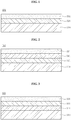
- FIG. 1 is a cross-sectional view illustrating a plastic substrate 101 according to the first exemplary embodiment.
- the plastic substrate 101 includes a plastic support member 310 having a light-transmitting characteristic (e.g., a transparent plastic support member), a first inorganic layer 321 on a surface of the plastic support member 310, and a first organic-inorganic hybrid layer 331 on the first inorganic layer 321.
- a plastic support member 310 having a light-transmitting characteristic e.g., a transparent plastic support member
- a first inorganic layer 321 on a surface of the plastic support member 310
- a first organic-inorganic hybrid layer 331 on the first inorganic layer 321.
- the first inorganic layer 321 includes a silicone resin.
- the first organic-inorganic hybrid layer 331 includes a polymer resin and inorganic particles dispersed in the polymer resin.
- a light-transmissive plastic film may be used as the plastic support member 310 on which the first inorganic layer 321 and the first organic-inorganic hybrid layer 331 are disposed.
- PE polyethylene
- PP polypropylene
- PA polyamide
- POM polyacetal film
- PMMA polymethyl methacrylate
- PET polyethylene terephthalate
- PBT polybutylene terephthalate
- PC polycarbonate
- a plastic film including a copolymer of polycarbonate (PC) and polymethyl methacrylate (PMMA) may be used as the plastic support member 310.
- polycarbonate (PC) is present in an amount of 50 wt% to 70 wt% and polymethyl methacrylate (PMMA) is present in an amount of 30 wt% to 50 wt%, with respect to the total weight of the copolymer of polycarbonate (PC) and polymethyl methacrylate (PMMA).
- a copolymer of which a content ratio (e.g., a weight ratio) in terms of polycarbonate (PC) to polymethyl methacrylate (PMMA) is 6:4 may be used as the plastic support member 310.
- the plastic support member 310 may have a thickness of 400 ⁇ m to 1000 ⁇ m. In a case where the thickness of the plastic support member 310 is less than 400 ⁇ m, the support strength of the plastic support member 310 may decrease, and in a case where the thickness thereof is more than 1000 ⁇ m, it is disadvantageous to achieve thinness of an element (e.g., the plastic support member 310 is too thick).
- the first inorganic layer 321 may have a thickness of 3 ⁇ m to 10 ⁇ m. In a case where the first inorganic layer 321 has a thickness less than 3 ⁇ m, the hardness of the plastic substrate 101 may decrease. In addition, in a case where the first inorganic layer 321 has a thickness more than 10 ⁇ m, it is disadvantageous in achieving thinness of an element (e.g., the first inorganic layer 321 is too thick).
- the first organic-inorganic hybrid layer 331 includes a polymer resin and inorganic particles dispersed in the polymer resin.
- the polymer resin used in the formation of the first organic-inorganic hybrid layer 331 has a light-transmitting characteristic, and the type (or kind) of the polymer resin is not particularly limited.
- the polymer resin may use, for example, one selected from an acrylic resin, a urethane resin and a urethane-acrylate resin.
- the first organic-inorganic hybrid layer 331 may be formed through polymerization and curing of a coating solution (a coating composition) for forming an organic-inorganic hybrid layer including an organic binder component and inorganic particles dispersed in the organic binder component.
- a coating solution for forming an organic-inorganic hybrid layer
- the coating solution (the coating composition) for forming an organic-inorganic hybrid layer is described in more detail below.
- the type (or kind) of the inorganic particle is not particularly limited.
- the inorganic particles may be silica particles or consist of zirconium oxide, aluminum oxide (Al 2 O 3 ), tantalum oxide, and nickel oxide.
- the inorganic particle is present in an amount of 30 wt% to 50 wt% with respect to the total weight of the first organic-inorganic hybrid layer 331.
- the polymer resin and the inorganic particle may have a content ratio (weight ratio) of about 6:4.
- the inorganic particles included in the first organic-inorganic hybrid layer 331 are present in an amount less than 30 wt%, the hardness of the first organic-inorganic hybrid layer 331 may decrease.
- the first organic-inorganic hybrid layer 331 may further include fluorine-containing compound in an amount of 0.001 wt% to 0.2 wt% with respect to the total weight of the first organic-inorganic hybrid layer 331.
- the fluorine (F) may serve as an additive in a small amount.
- the hardness of the first organic-inorganic hybrid layer 331 may increase.
- the first organic-inorganic hybrid layer 331 has a thickness of 5 ⁇ m to 15 ⁇ m. In a case where the first organic-inorganic hybrid layer 331 has a thickness less than 5 ⁇ m, the first organic-inorganic hybrid layer 331 may experience difficulty in having a sufficient (or suitable) hardness, and in a case where the first organic-inorganic hybrid layer 331 has a thickness more than 15 ⁇ m, it is disadvantageous in achieving thinness of an element (e.g., the first organic-inorganic hybrid layer 331 is too thick).
- FIG. 2 is a cross-sectional view illustrating a plastic substrate 102 according to the second exemplary embodiment.
- the plastic substrate 102 includes a plastic support member 310 having a light-transmitting characteristic, a first inorganic layer 321 on a surface of the plastic support member 310, a first organic layer 341 on the first inorganic layer 321, and a first organic-inorganic hybrid layer 331 on the first organic layer 341.
- the first organic layer 341 may include at least one selected from an acrylic resin, a urethane resin and a urethane-acrylate resin.
- the first organic layer 341 may be formed through curing of a coating solution (a coating composition) for forming an organic layer.
- a coating solution for forming an organic layer.
- the coating solution (the coating composition) for forming an organic layer is described in more detail below.
- the first organic layer 341 is disposed between the first inorganic layer 321 and the first organic-inorganic hybrid layer 331 to serve as a buffer with respect to stress caused among the layers.
- the first organic layer 341 has a thickness of 5 ⁇ m to 10 ⁇ m. In a case where the thickness of the first organic layer 341 is less than 5 ⁇ m, buffer effects may hardly occur among the layers, and in a case where the thickness thereof is more than 10 ⁇ m, it is disadvantageous in achieving thinness of an element (e.g., the first organic layer 341 is too thick).
- FIG. 3 is a cross-sectional view illustrating a plastic substrate 103 according to the third exemplary embodiment.
- the plastic substrate 103 includes a plastic support member 310 having a light-transmitting characteristic, a first organic layer 341 on a surface of the plastic support member 310, a first inorganic layer 321 on the first organic layer 341, and a first organic-inorganic hybrid layer 331 on the first inorganic layer 321.
- the plastic substrate 103 according to the third exemplary embodiment is the same as the plastic substrate 102 according to the second exemplary embodiment, except for the position of the first organic layer 341.
- the first organic layer 341 is disposed between the plastic support member 310 and the first inorganic layer 321 to serve as a buffer with respect to stress caused among the layers.
- FIG. 4 is a cross-sectional view illustrating a plastic substrate 104 according to the fourth exemplary embodiment.
- the plastic substrate 104 includes a plastic support member 310 having a light-transmitting characteristic, a first inorganic layer 321 and a second inorganic layer 322 that are disposed on both sides of the plastic support member 310, respectively, and a first organic-inorganic hybrid layer 331 and a second organic-inorganic hybrid layer 332 on the first inorganic layer 321 and the second inorganic layer 322, respectively.
- the plastic substrate 104 according to the fourth exemplary embodiment further includes the second inorganic layer 322 on another surface (e.g., a second surface) of the plastic support member 310 and the second organic-inorganic hybrid layer 332 on the second inorganic layer 322 as compared to the plastic substrate 101 according to the first exemplary embodiment.
- the second inorganic layer 322 has a composition the same as that of the first inorganic layer 321, and the second organic-inorganic hybrid layer 332 has a composition the same as that of the first organic-inorganic hybrid layer 331.
- FIG. 5 is a cross-sectional view illustrating a plastic substrate 105 according to the fifth exemplary embodiment.
- the plastic substrate 105 according to the fifth exemplary embodiment further includes a first organic layer 341 between a first inorganic layer 321 and a first organic-inorganic hybrid layer 331 and a second organic layer 342 between a second inorganic layer 322 and a second organic-inorganic hybrid layer 332, as compared to the plastic substrate 104 according to the fourth exemplary embodiment.
- the first inorganic layer 321 and the second inorganic layer 322 are on respective surfaces of the plastic support member 310.
- FIG. 6 is a cross-sectional view illustrating a plastic substrate 106 according to the sixth exemplary embodiment.
- the plastic substrate 106 further includes a first organic layer 341 between a plastic support member 310 and a first inorganic layer 321 and a second organic layer 342 between the plastic support member 310 and a second inorganic layer 322, as compared to the plastic substrate 104 according to the fourth exemplary embodiment.
- the plastic substrate 106 further includes the first organic-inorganic hybrid layer 331 and the second organic-inorganic hybrid layer 332.
- the plastic support member 310 having a light-transmitting characteristic is immersed in the coating solution (the coating composition) for forming an inorganic layer to thereby form the first inorganic layer 321 and the second inorganic layer 322 on both sides of the plastic support member 310, respectively, and subsequently, the plastic support member 310 formed with the first inorganic layer 321 and the second inorganic layer 322 is immersed in the coating solution (the coating composition) for forming an organic-inorganic hybrid layer to thereby form the first organic-inorganic hybrid layer 331 on the first inorganic layer 321 and the second organic-inorganic hybrid layer 332 on the second inorganic layer 322.
- the first inorganic layer 321 and the second inorganic layer 322 may also be collectively referred to as inorganic layers 321 and 322, and the first organic-inorganic hybrid layer 331 and the second organic-inorganic hybrid layer 332 may also be collectively referred to as organic-inorganic hybrid layers 331 and 332.
- the inorganic layers 321 and 322 and the organic-inorganic hybrid layers 331 and 332 are formed on the both sides of the plastic support member 310.
- the plastic support member 310 includes one selected from the group consisting of: a polyethylene (PE) film, a polypropylene (PP) film, a polyamide (PA) film, a polyacetal (polyoxymethylene, POM) film, a polymethyl methacrylate (PMMA) film, a polyethylene terephthalate (PET) film, a polybutylene terephthalate (PBT) film, a polycarbonate (PC) film, a cellulose film, and a moisture-resistant cellophane.
- the plastic support member 310 may include a combination of the foregoing.
- the terms “combination thereof” and “combinations thereof” may refer to a mixture or a laminated structure of components.
- a copolymer of polycarbonate (PC) and polymethyl methacrylate (PMMA) in which polycarbonate (PC) is present in an amount of 50 wt% to 70 wt% and polymethyl methacrylate (PMMA) is present in an amount of 30 wt% to 50 wt% with respect to the total weight of the copolymer of polycarbonate (PC) and polymethyl methacrylate (PMMA) may be used for forming the plastic support member 310.
- the forming of the inorganic layers 321 and 322 includes immersing the plastic support member 310 in the coating solution (the coating composition) for forming an inorganic layer to thereby form inorganic coating layers on the both sides of the plastic support member 310 and thermal-curing the inorganic coating layers.
- the coating solution (the coating composition) for forming an inorganic layer includes a silicone monomer with a coupling moiety.
- the coupling moiety may include, for example, an epoxy group, an acrylic group, and a vinyl group.
- silicone monomer examples are represented by the following Chemical Formula 5 and Chemical Formula 6, which may be used solely or in combination with each other.
- R21, R22, R23, and R24 are independently selected from an amino group, an epoxy group, a phenyl group, an acrylic group, and a vinyl group. At least one of R21, R22, R23, and R24 is an acrylic group or a vinyl group.
- R25 and R26 are independently selected from hydrogen (H) and a hydrocarbon group having 1 to 6 carbon atoms (for example a C1-C6 alkyl group, especially a methyl group or ethyl group).
- the coupling moiety is present in an amount of about 5 wt% to about 15 wt% with respect to the total weight of the coating solution for forming an inorganic layer.
- the coating solution may be a hybrid sol.
- An acrylic group increases adhesion and density of the inorganic layers 321 and 322, a vinyl group increases flexibility, and a phenyl group increases thermal-resistance.
- the inorganic coating layer is thermally-cured.
- the thermal-curing may be performed at a relatively low temperature.
- the thermal-curing may be performed at a temperature of 60 °C to 120 °C.
- the inorganic layer may be formed without employing schemes such as sputtering or deposition that are performed at a high temperature. Accordingly, damages to the plastic support member 310 due to heat may be prevented or reduced.
- the forming of the organic-inorganic hybrid layers 331 and 332 includes: immersing the plastic support member 310 formed with the inorganic layers 321 and 322 in the coating solution for forming an organic-inorganic hybrid layer to thereby form a coating layer for forming an organic-inorganic hybrid layer on both sides of the inorganic layers 321 and 322, and photo-curing the coating layer for forming an organic-inorganic hybrid layer.
- ultraviolet (UV) light irradiation may be utilized for the photo-curing.
- the coating solution for forming an organic-inorganic hybrid layer includes an organic binder component and inorganic particles dispersed in the organic binder component.
- the organic binder component includes a monomer, an oligomer, and a photoinitiator, for example, a photopolymerization initiator.
- the monomer may include at least one selected from an acrylic monomer and a urethane monomer.
- an organic binder is formed by polymerization of the organic binder component, i.e. the organic binder is a polyacrylate or a polyurethane.
- the organic binder component may also be used to form the organic layers 341 and 342.
- the organic binder component may include a monomer in an amount of 20 wt% to 60 wt%, an oligomer in an amount of 20 wt% to 60 wt, a rubber-based elastic component in an amount of 10 wt% to 50 wt%, and a photoinitiator in an amount of 1 wt% to 10 wt%, where the wt% may be based on the total weight of the organic binder component.
- the monomer may use a monofunctional monomer and/or a polyfunctional monomer.
- the monofunctional monomer may include an acrylic monomer such as nonylphenyl carbitol acrylate, 2-hydroxy-3-phenoxypropyl acrylate, 2-ethylhexyl carbitol acrylate, and 2-hydroxyethyl acrylate.
- an acrylic monomer such as nonylphenyl carbitol acrylate, 2-hydroxy-3-phenoxypropyl acrylate, 2-ethylhexyl carbitol acrylate, and 2-hydroxyethyl acrylate.
- a vinyl-based monomer such as N-vinylpyrrolidone may be added thereto.
- the polyfunctional monomer having two or more reactive groups may include an acrylic monomer such as 1,6-hexanediol di(meth)acrylate, ethyleneglycol di(meth)acrylate, neopentylglycol di(meth)acrylate, triethyleneglycol di(meth)acrylate, and 3-methyl pentanediol di(meth)acrylate.
- an acrylic monomer such as 1,6-hexanediol di(meth)acrylate, ethyleneglycol di(meth)acrylate, neopentylglycol di(meth)acrylate, triethyleneglycol di(meth)acrylate, and 3-methyl pentanediol di(meth)acrylate.
- the polyfunctional monomers may include trimethylolpropane tri(meth)acrylate, ethoxylated trimethylolpropane tri(meth)acrylate, propoxylated trimethylolpropane tri(meth)acrylate, pentaerythritol tri(meth)acrylate, pentaerythritol tetra(meth)acrylate, dipentaerythritol penta(meth)acrylate, ethoxylated dipentaerythritol hexa(meth)acrylate, propoxylated di pentaerythritol hexa(meth)acrylate, and dipentaerythritol hexa(meth)acrylate.
- (meth)acrylate may refer to one selected from acrylate and methacrylate or may refer to both acrylate and methacrylate.
- the monomer may be used solely or in combination of two or more kinds thereof.
- the oligomer may use or include urethane (meth)acrylate oligomers having a weight-average molecular weight (Mw) of about 5,000 to about 50,000.
- Mw weight-average molecular weight
- the coating solution (the coating composition) for forming an organic-inorganic hybrid layer may experience difficulty in maintaining a solid state at room temperature.
- the urethane (meth) acrylate may be formed by reaction of a polyol compound having two or more hydroxyl groups in the molecule, a compound having two or more isocyanate groups in the molecule, and (meth) acrylate having one or more hydroxyl groups in the molecule.
- the polyol compound having two or more hydroxyl groups in the molecule may include, for example, polyether polyol, polyester polyol, caprolactone diol, bisphenol polyol, polyisoprene polyol, hydrogenated polyisoprene polyol, polybutadiene polyol, hydrogenated polybutadiene polyol, castor oil polyol, and/or polycarbonate diol, which may be used solely or in combination of two or more thereof.
- the compound having two or more isocyanate groups in the molecule may include, for example, aromatic polyisocyanate, alicyclic polyisocyanate, and aliphatic polyisocyanate, which may be used solely or in combination of two or more thereof.
- the (meth)acrylate having at least one hydroxyl group in the molecule may include: for example, mono(meth)acrylate of dihydric alcohols, such as ethylene glycol, propylene glycol, 1,3-propanediol, 1,3-butanediol, 1,4-butanediol, and polyethylene glycol; mono(meth)acrylate of trihydric alcohols, such as trimethylolethane, trimethylolpropane, and glycerin; and/or di(meth)acrylate, which may be used solely or in combination of two or more thereof.
- dihydric alcohols such as ethylene glycol, propylene glycol, 1,3-propanediol, 1,3-butanediol, 1,4-butanediol, and polyethylene glycol
- mono(meth)acrylate of trihydric alcohols such as trimethylolethane, trimethylolpropane, and glycerin
- the oligomer for example, may use silicone acrylate represented by the following Chemical Formula 8:
- n is an integer in a range of 5 to 50.
- the silicone acrylate represented by Chemical Formula 8 includes silicon (Si) and has excellent affinity for the inorganic layers 321 and 322.
- the rubber-based elastic component may include at least one selected from polybutadiene and polyisoprene each having a weight-average molecular weight (Mw) of about 10,000 to about 100,000.
- the rubber-based elastic component may impart elasticity to the coating solution (the coating composition) for forming an organic-inorganic hybrid layer.
- the coating solution (the coating composition) for forming an organic-inorganic hybrid may have stable fluidity.
- the photoinitiator may absorb activation energy rays, such as UV rays, to generate radicals.
- the radicals generated from the photoinitiator react with the monomer and/or the oligomer to initiate a polymerization reaction of an adhesive composition.
- a cross-linking reaction may occur among the monomer, the oligomer, and the rubber-based elastic component.
- the coating solution (the coating composition) for forming an organic-inorganic hybrid layer is cured to thereby form the organic-inorganic hybrid layer.
- the inorganic particles may be formed of at least one selected from a silica, zirconium oxide, aluminum oxide, tantalum oxide, and nickel oxide.
- the inorganic particle is present in an amount of 30 wt% to 50 wt% with respect to the total weight of the coating solution for forming an organic-inorganic hybrid layer.
- the coating solution for forming an organic-inorganic hybrid layer may further include a fluorine-containing compound in an amount of 0.001 wt% to 0.2 wt% with respect to the total weight of the coating solution (the coating composition) for forming an organic-inorganic hybrid layer.
- Fluorine (F) is provided in a form of a chemical composition represented by the following Chemical Formula 9, and may be included in the coating solution (the coating composition) for forming an organic-inorganic hybrid layer.
- R31 and R32 are independently selected from a hydrocarbon group having 1 to 6 carbon atoms or a fluorinated C1-C6 alkyl group, and m and n each independently are integers in a range of 1 to 20.
- the plastic substrate 104 illustrated in FIG. 4 is manufactured.
- the organic layers 341 and 342 may be formed on the inorganic layers 321 and 322.
- the plastic substrate 105 illustrated in FIG. 5 may be manufactured.
- the organic layers 341 and 342 may be formed on the both sides of the plastic support member 310, and the inorganic layers 321 and 322 and the organic-inorganic hybrid layers 331 and 332 may be sequentially formed thereon.
- the plastic substrate 106 illustrated in FIG. 6 may be manufactured.
- the organic layers 341 and 342 may be formed through a dip coating method using the coating solution (the coating composition) for forming an organic layer formed of an organic binder component.
- the coating solution (the coating composition) for forming an organic layer may use an organic binder component used for manufacturing the coating solution (the coating composition) for forming an organic-inorganic hybrid layer.
- the organic binder component for forming the organic layer includes a monomer, an oligomer, and a photoinitiator.
- the monomer may include at least one selected from an acrylic monomer and a urethane monomer.
- the coating solution (the coating composition) for forming an organic layer may include a monomer in an amount of 20 wt% to 60 wt%, an oligomer in an amount of 20 wt% to 60 wt, a rubber-based elastic component in an amount of 10 wt% to 50 wt%, and a photoinitiator in an amount of 1 wt% to 10 wt %, where the foregoing wt% may be based on the total weight of the coating solution.
- the organic layers 341 and 342 formed in such a manner include at least one selected from an acrylic resin, a urethane resin, and a urethane-acrylate resin.
- An acrylic group of the organic layers 341 and 342 exhibits excellent affinity for the plastic support member 310 and the inorganic layers 321 and 322 and for the organic-inorganic hybrid layers 331 and 332.
- the organic layers 341 and 342 and the organic-inorganic hybrid layers 331 and 332 may form a bond represented by the following Chemical Formula 11 at an interface.
- OR represents the organic layers 341 and 342.
- the organic layers 341 and 342 may bond with a silica particle (Si-O) included in the organic-inorganic hybrid layers 331 and 332.
- the hardness of the coating layers including the inorganic layer, the organic layer, and the organic-inorganic hybrid layer may be improved.
- an experimental sample including the plastic substrate 104 according to the fourth exemplary embodiment is referred to as "experimental example 1”
- an experimental sample including the plastic substrate 105 according to the fifth exemplary embodiment is referred to as "experimental example 2”
- an experimental sample including the plastic substrate 106 according to the sixth exemplary embodiment is referred to as "experimental example 3.”
- a plastic support member 310 is a polycarbonate (PC) film having a thickness of about 550 ⁇ m
- inorganic layers 321 and 332 are layers having the repeating unit represented by Chemical Formula 2
- organic-inorganic hybrid layers 331 and 322 are layers including a polymer resin, containing urethane acrylate, in an amount of about 60 wt% (e.g., based on the total weight of the organic-inorganic hybrid layers) and silica particles, dispersed in the polymer resin, in an amount of about 40 wt%
- organic layers 341 and 342 are urethane-acrylate layers.
- the experimental sample of the experimental example 1 has a structure in which an organic-inorganic hybrid layer having a thickness of about 10 ⁇ m, an inorganic layer having a thickness of about 5 ⁇ m, a plastic support member having a thickness of about 550 ⁇ m, an inorganic layer having a thickness of about 5 ⁇ m, and an organic-inorganic hybrid layer having a thickness of about 10 ⁇ m are sequentially disposed.
- the experimental sample of the experimental example 2 has a structure in which an organic-inorganic hybrid layer having a thickness of about 5 ⁇ m, an organic layer having a thickness of about 10 ⁇ m, an inorganic layer having a thickness of about 5 ⁇ m, a plastic support member having a thickness of about 550 ⁇ m, an inorganic layer having a thickness of about 5 ⁇ m, an organic layer having a thickness of about 10 ⁇ m, and an organic-inorganic hybrid layer having a thickness of about 5 ⁇ m are sequentially disposed.
- the experimental sample of the experimental example 3 has a structure in which an organic-inorganic hybrid layer having a thickness of about 5 ⁇ m, an inorganic layer having a thickness of about 10 ⁇ m, an organic layer having a thickness of about 5 ⁇ m, a plastic support member having a thickness of about 550 ⁇ m, an organic layer having a thickness of about 5 ⁇ m, an inorganic layer having a thickness of about 10 ⁇ m, and an organic-inorganic hybrid layer having a thickness of about 5 ⁇ m are sequentially disposed.
- a plastic substrate including only a polycarbonate (PC) film having a thickness of about 550 ⁇ m (comparative example 1), a plastic substrate including organic-inorganic hybrid layers having a thickness of about 10 ⁇ m formed on both sides of a polycarbonate (PC) film having a thickness of about 550 ⁇ m through a dip coating method (comparative example 2), and a plastic substrate including organic-inorganic hybrid layers having a thickness of about 20 ⁇ m formed on both sides of a polycarbonate (PC) film having a thickness of about 550 ⁇ m through a spray coating method (comparative example 3) are used.
- PC polycarbonate
- An experimental sample having a size of 150 mm x 100 mm is manufactured using a plastic substrate, the pencil hardness is measured five times on the experimental sample with respect to a weight of 1 kg in accordance with the pencil hardness test specified in JIS K 5600-5-4, and the smallest value is selected as a pencil hardness of the experimental sample.
- the "H” lead or a “B” lead increases, the "H” lead becomes harder, whereas the “B” lead becomes smoother.
- “9H” denotes a highest hardness, and the hardness decreases in the following order: 8H, 7H, 6H, 5H, 4H, 3H, 2H, H, F, B, 2B, 3B, 4B, 5B, 6B, 7B, 8B, and 9B.
- An experimental sample having a size of 200 mm x 200 mm is manufactured using a plastic substrate, and a cylinder, having a diameter of about 25 mm, of which a flat surface is uniformly attached with a steel wool #0000 is prepared. Subsequently, a surface of the experimental sample is rubbed with the cylinder attached with the steel wool #0000 thirty times with a weight of 1.0 kg at a speed of about 100 mm a second, and the number of scratches appearing on the surface of the experimental sample is identified with the unaided eye.
- An iron ball of 22 g is spaced apart from the experimental sample to be dropped thereto so as to identify whether a crack occurs.
- the dropping of the iron ball is repeatedly carried out while increasing a dropping height of the iron ball to verify a dropping height that causes a crack.
- the dropping height of the iron ball is increased from 5 cm to 20 cm.
- Transmittance, reflectivity, and haze are measured using a spectrophotometer (device name: "COH-400").
- the experimental samples of the experimental examples 1, 2, and 3 according to the fourth, fifth, and sixth exemplary embodiments have a pencil hardness of 6H or more, and have excellent scratch-resistance and excellent impact-resistance. Accordingly, the plastic substrates 104, 105, and 106 according to the fourth, fifth, and sixth exemplary embodiments have mechanical properties substantially equivalent to those of glass. Further, the experimental samples of the experimental examples 1, 2, and 3 have excellent optical properties.
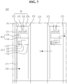
- FIG. 7 is a plan view illustrating a display device according to the seventh exemplary embodiment
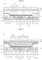
- FIG. 8 is a cross-sectional view taken along line I-I' of FIG. 7 .
- the display device 107 includes a display panel 110, an adhesive layer 290 on the display panel 110, a plastic substrate 101 on the adhesive layer 290.
- the plastic substrate 101 on the adhesive layer 290 is a window protecting the display panel 110.
- the display panel 110 is configured to display images.
- the display panel 110 is not particularly limited.
- the display panel 110 may use a self-emission-type display panel (a self-emission kind of display panel) such as an organic light emitting display panel or a non-emission-type display panel (a non-emission kind of display panel) such as a liquid crystal display (“LCD”) panel, an electrowetting display panel, an electrophoretic display panel (“EPD”), or a microelectromechanical system (“MEMS”) display panel.
- the display device may include a backlight unit configured to provide light to the display panel 110.
- a polarizer may be disposed between the display panel 110 and the plastic substrate 101.
- the polarizer may prevent or reduce reflection of externally incident light (external light) from the display panel 110 so as not to be perceived by a user.
- the display device 107 may further include a touch screen panel.
- the touch screen panel may be disposed between the display panel 110 and the polarizer.
- the display panel 110 may use an organic light emitting display panel.
- the display device according to the seventh exemplary embodiment is an organic light emitting diode (“OLED”) display device, but the seventh exemplary embodiment is not limited thereto.
- the display panel 110 includes a first substrate 111, a wiring unit 130, an OLED 210, and a second substrate 112.
- the first substrate 111 may include an insulating material including one selected from the group consisting of: glass, quartz, ceramic, plastic and the like.
- the first substrate 111 may be formed of a metal material such as stainless steel.
- a buffer layer 121 is disposed on the first substrate 111.
- the buffer layer 121 may include one or more layer selected from various suitable inorganic layers and organic layers.
- the buffer layer 121 may significantly reduce infiltration of undesirable elements such as moisture into the wiring unit 130 or the OLED 210 and also planarize a surface.
- the buffer layer 121 may not be invariably necessary, and may be omitted.
- the wiring unit 130 is disposed on the buffer layer 121.
- the wiring unit 130 is a portion including a switching thin film transistor ("TFT") 10, a driving TFT 20, and a capacitor 80, and is configured to drive the OLED 210.
- the OLED 210 may display an image by emitting light based on a driving signal applied from the wiring unit 130.
- FIGS. 7 and 8 illustrate an active-matrix-type (an active-matrix kind of) organic light emitting diode (“AMOLED”) display having a 2Tr-1 Cap structure, which includes two TFTs, for example the switching TFT 10 and the driving TFT 20, and the capacitor 80 in each pixel.
- AMOLED organic light emitting diode
- the display device according to the seventh exemplary embodiment is not limited thereto.
- the OLED display device 107 may include three or more TFTs and two or more capacitors 80 in each pixel, and may further include additional wirings to have various suitable structures.
- the term "pixel” refers to the smallest unit for displaying an image, and the display area displays an image using a plurality of pixels.
- Each of the pixels includes the switching TFT 10, the driving TFT 20, the capacitor 80, and the OLED 210.
- a gate line 151 disposed along one direction and a data line 171 and a common power line 172 insulated from and intersecting the gate line 151 are disposed on the wiring unit 130.
- each pixel may be defined by the gate line 151, the data line 171, and the common power line 172, but is not limited thereto.
- the pixel may be defined by a pixel defining layer (PDL) or a black matrix.
- the OLED 210 may include a first electrode 211, an organic light emitting layer 212 formed on the first electrode 211, and a second electrode 213 formed on the organic light emitting layer 212. Holes and electrons are injected to the organic light emitting layer 212 from the first electrode 211 and the second electrode 213, respectively. The injected holes and electrons are combined with each other to form an exciton, and then light is emitted by energy generated when the exciton falls (e.g., relaxes) from an excited state to a ground state.
- the capacitor 80 includes a pair of storage electrodes 158 and 178 with an insulating interlayer 145 interposed therebetween.
- the insulating interlayer 145 may include a dielectric material. Capacitance of the capacitor 80 is determined by electric charges accumulated in the capacitor 80 and voltage across the pair of storage electrodes 158 and 178.
- the switching TFT 10 includes a switching semiconductor layer 131, a switching gate electrode 152, a switching source electrode 173, and a switching drain electrode 174.
- the driving TFT 20 includes a driving semiconductor layer 132, a driving gate electrode 155, a driving source electrode 176, and a driving drain electrode 177.
- the semiconductor layers 131 and 132 and the gate electrodes 152 and 155 are insulated from a gate insulating layer 141.
- the switching TFT 10 may function as a switching element which selects a pixel to perform light emission.
- the switching gate electrode 152 is connected to the gate line 151, and the switching source electrode 173 is connected to the data line 171.
- the switching drain electrode 174 is spaced apart from the switching source electrode 173 and connected to one of the storage electrodes 158.
- the driving TFT 20 may apply a driving power to the first electrode 211, which serves as a pixel electrode, so as to allow the organic light emitting layer 212 of the OLED 210 in a selected pixel to emit light.
- the driving gate electrode 155 is connected to the storage electrode 158 that is connected to the switching drain electrode 174.
- the driving source electrode 176 and the other of the storage electrodes 178 each are connected to the common power line 172.
- the switching TFT 10 may be operated by a gate voltage applied to the gate line 151 and may function to transmit, to the driving TFT 20, a data voltage applied to the data line 171. Voltage equivalent to a difference between a common voltage applied from the common power line 172 to the driving TFT 20 and the data voltage transmitted from the switching TFT 10 may be stored in the capacitor 80, and current corresponding to the voltage stored in the capacitor 80 may flow to the OLED 210 through the driving TFT 20, so that the OLED 210 may emit light.
- the first electrode 211 is an anode serving as a hole injection electrode
- the second electrode 213 is a cathode serving as an electron injection electrode.
- the seventh exemplary embodiment is not limited thereto.
- the first electrode 211 may be a cathode and the second electrode 213 may be an anode.
- a planarization layer 146 is disposed on the insulating interlayer 145.
- the planarization layer 146 may be formed of an insulating layer, and protect the wiring unit 130.
- the planarization layer 146 and the insulating interlayer 145 may be formed of the same (e.g., substantially the same) material.
- the driving drain electrode 177 of the driving TFT 20 is connected to the first electrode 211 of the OLED 210 through a contact hole defined in the planarization layer 146.
- the first electrode 211 is a reflective electrode and the second electrode 213 is a transflective electrode. Accordingly, light emitted from the organic light emitting layer 212 may be transmitted through the second electrode 213 to be emitted.
- the reflective electrode and the transflective electrode one or more metal selected from: magnesium (Mg), silver (Ag), gold (Au), calcium (Ca), lithium (Li), chromium (Cr), aluminum (Al), and copper (Cu), or an alloy thereof may be used.
- Mg magnesium
- silver Au
- Au gold
- Ca calcium
- Li lithium
- Cr chromium
- Al aluminum
- Cu copper
- whether the electrode is a reflective type (a reflective kind) or a transflective type (a transflective kind) may be determined based on a thickness of the electrode.
- the transflective layer has a thickness of 200 nm or less. As the thickness of the transflective layer decreases, a level of light transmittance may increase, and as the thickness thereof increases, the light transmittance may decrease.
- the first electrode 211 may include a reflective layer including at least one metal selected from magnesium (Mg), silver (Ag), gold (Au), calcium (Ca), lithium (Li), chromium (Cr), aluminum (Al), and copper (Cu), and a transparent conductive layer disposed on the reflective layer.
- the transparent conductive layer may include a transparent conductive oxide (TCO), for example, at least one selected from indium tin oxide (ITO), indium zinc oxide (IZO), zinc oxide (ZnO), aluminum zinc oxide (AZO), and indium oxide (In 2 O 3 ). Since such a transparent conductive layer has a relatively high work function, hole injection through the first electrode 211 may be readily performed.
- the first electrode 211 may have a triple-layer structure in which a transparent conductive layer, a reflective layer, and a transparent conductive layer are sequentially stacked.
- the second electrode 213 may include a transflective layer including at least one metal of magnesium (Mg), silver (Ag), gold (Au), calcium (Ca), lithium (Li), chromium (Cr), aluminum (Al), and copper (Cu).
- Mg magnesium
- Ag silver
- Au gold
- Ca calcium
- Li lithium
- Cr chromium
- Al aluminum
- Cu copper
- At least one selected from a hole injection layer (HIL) and a hole transporting layer (HTL) may further be disposed between the first electrode 211 and the organic light emitting layer 212.
- at least one selected from an electron transporting layer (ETL) and an electron injection layer (EIL) may further be disposed between the organic light emitting layer 212 and the second electrode 213.
- the organic light emitting layer 212, the HIL, the HTL, the ETL, and the EIL may be collectively referred to as an organic layer.
- Such an organic layer may be formed of a low molecular weight organic material or a polymer organic material.
- the pixel defining layer 191 has an aperture.
- the aperture of the pixel defining layer 191 exposes a portion of the first electrode 211.
- the first electrode 211, the organic light emitting layer 212, and the second electrode 213 are sequentially stacked in the aperture of the pixel defining layer 191.
- the second electrode 213 may be disposed on the organic light emitting layer 212 and on the pixel defining layer 191.
- the OLED 210 emits light from the organic light emitting layer 212 disposed in the aperture of the pixel defining layer 191. Accordingly, the pixel defining layer 191 may define a light emission area.
- a capping layer may further be disposed on the second electrode 213.
- the capping layer may protect the OLED 210.
- a second substrate 112 is disposed on the OLED 210 to face the first substrate 111.
- the second substrate 112 may be formed of the same (e.g., substantially the same) material as a material forming the first substrate 111.
- the first substrate 111 and the second substrate 112 may be sealed by a sealant.
- a buffer member 202 is disposed between the OLED 210 and the second substrate 112.
- the buffer member 202 may protect interior components, such as the OLED 210, from impact that may be externally imposed to the OLED display device 107.
- the buffer member 202 may enhance device reliability of the OLED display device 107.
- the buffer member 202 may include at least one of an organic sealant, such as a urethane-based resin, an epoxy-based resin, and an acrylic resin, or an inorganic sealant, such as silicon (or silicone).
- the adhesive layer 290 is disposed on the display panel 110, and the plastic substrate 101 is disposed on the adhesive layer 290.
- a side of the plastic substrate 101 on which the first inorganic layer 321 and the first organic-inorganic hybrid layer 331 are disposed is opposite to a side on which the display panel 110 is disposed.
- the plastic substrate 101 may serve as a window protecting the display panel 110.
- the seventh exemplary embodiment is not limited thereto, and the plastic substrates 102, 103, 104, 105, and 106 according to the second to sixth exemplary embodiments may be used as the window.
- FIG. 9 is a plan view illustrating a display device 108 according to the eighth exemplary embodiment.
- the display device 108 includes a thin film encapsulation film 250 on the OLED 210.
- the thin film encapsulation layer 250 includes one or more inorganic layers 251, 253, and 255 and one or more organic layers 252 and 254.
- the thin film encapsulation layer 250 has a structure in which the inorganic layers 251, 253, and 255 and the organic layers 252 and 254 are alternately stacked.
- the inorganic layer 251 may be disposed as a lowermost layer of the stacked structure of the thin film encapsulation layer 250.
- the inorganic layer 251 may be disposed to be most adjacent to the OLED 210.
- FIG. 9 illustrates the thin film encapsulation layer 250 as including the three inorganic layers 251, 253, and 255 and the two organic layers 252 and 254, the exemplary embodiment is not limited thereto.
- the inorganic layers 251, 253, and 255 may include one or more of the following inorganic materials: Al 2 O 3 , TiO 2 , ZrO, SiO 2 , AlON, AlN, SiON, Si 3 N4, ZnO, Ta 2 O 5 , SiO x (0 ⁇ x ⁇ 3), and SiN x (0 ⁇ x ⁇ 3/4).
- the inorganic layers 251, 253, and 255 may be formed through a chemical vapor deposition (CVD) process or an atomic layer deposition (ALD) process.
- CVD chemical vapor deposition
- ALD atomic layer deposition
- the eighth exemplary embodiment is not limited thereto, and the inorganic layers 251, 253, and 255 may be formed through various suitable processes available in the pertinent art.
- the organic layers 252 and 254 may include or be formed of a polymer-based material.
- the polymer-based material may include an acrylic resin, an epoxy resin, polyimide, polyethylene, and the like.
- the organic layers 252 and 254 may be formed through various suitable methods available to those skilled in the pertinent art, such as a thermal deposition process.
- the thermal deposition process for forming the organic layers 252 and 254 is performed in a temperature range that may not damage the OLED 210.
- the eighth exemplary embodiment is not limited thereto, and the organic layers 252 and 254 may be formed through various suitable methods available to those skilled in the pertinent art.
- the inorganic layers 251, 253, and 255 formed to have a high density of a thin film may primarily serve to reduce or effectively prevent or reduce infiltration of moisture or oxygen thereinto.
- the infiltration of moisture or oxygen into the OLED 210 may be prevented or reduced largely by the inorganic layers 251, 253, and 255.
- Moisture or oxygen passing through the inorganic layers 251, 253, and 255 may be blocked further by the organic layers 252 and 254.
- the organic layers 252 and 254 may exhibit relatively low efficiency in preventing or reducing the moisture infiltration, as compared to the inorganic layers 251, 253, and 255.
- the organic layers 252 and 254 may also serve as a buffer layer to reduce stress between respective layers of the inorganic layers 251, 253, and 255 and the organic layers 252 and 254, in addition to the prevention or reduction of the moisture infiltration.
- an uppermost surface of the thin film encapsulation layer 250 may be planarized.
- the thin film encapsulation layer 250 may have a thickness of about 10 ⁇ m or less. Accordingly, an overall thickness of the OLED display device 108 may be significantly reduced.
- the second substrate 112 may be omitted. In a case where the second substrate 112 is omitted, the flexibility of the display device 108 may be improved.
- the plastic substrate includes the inorganic layer and the organic-inorganic hybrid layer on the plastic support member, thus having excellent hardness and abrasion-resistance. Further, the plastic substrate according to exemplary embodiments is used as the window of the display device, thus allowing the display device to be light-weighted.
Landscapes
- Chemical & Material Sciences (AREA)
- Organic Chemistry (AREA)
- Polymers & Plastics (AREA)
- Medicinal Chemistry (AREA)
- Chemical Kinetics & Catalysis (AREA)
- Health & Medical Sciences (AREA)
- Engineering & Computer Science (AREA)
- Materials Engineering (AREA)
- Physics & Mathematics (AREA)
- Life Sciences & Earth Sciences (AREA)
- Wood Science & Technology (AREA)
- Optics & Photonics (AREA)
- Inorganic Chemistry (AREA)
- Nonlinear Science (AREA)
- General Physics & Mathematics (AREA)
- Crystallography & Structural Chemistry (AREA)
- Mathematical Physics (AREA)
- Laminated Bodies (AREA)
- Theoretical Computer Science (AREA)
- Devices For Indicating Variable Information By Combining Individual Elements (AREA)
- Electroluminescent Light Sources (AREA)
- Application Of Or Painting With Fluid Materials (AREA)
- Coating Of Shaped Articles Made Of Macromolecular Substances (AREA)
- Polymerisation Methods In General (AREA)
- Addition Polymer Or Copolymer, Post-Treatments, Or Chemical Modifications (AREA)
Claims (15)
- Verfahren zur Herstellung eines Kunststoffsubstrats (101, 102, 103, 104, 105, 106), wobei das Verfahren umfasst:Eintauchen eines transparenten Kunststoffträgerelements (310) in eine Beschichtungslösung zum Bilden einer anorganischen Schicht und dadurch Bilden einer ersten anorganischen Schicht (321) und einer zweiten anorganischen Schicht (322) auf den jeweiligen Seiten des Kunststoffträgerelements (310); undEintauchen des mit der ersten anorganischen Schicht (321) und der zweiten anorganischen Schicht (322) gebildeten Kunststoffträgerelements (310) in eine Beschichtungslösung zum Bilden einer organisch-anorganischen Hybridschicht und damit Bilden einer ersten organisch-anorganischen Hybridschicht (331) und einer zweiten organisch-anorganischen Hybridschicht (332) auf der ersten anorganischen Schicht (321) bzw. der zweiten anorganischen Schicht (322),wobei die Beschichtungslösung zum Bilden der anorganischen Schichten (321, 322) ein Silikonmonomer mit einem Kopplungsfragment umfasst, unddie Beschichtungslösung zum Bilden einer organisch-anorganischen Hybridschicht (331, 332) eine organische Bindemittelkomponente und anorganische Partikel umfasst, die in der organischen Bindemittelkomponente dispergiert sind.
- Verfahren nach Anspruch 1, wobei das Silikonmonomer mindestens eines umfasst, das ausgewählt ist aus einem Monomer, dargestellt durch die folgende chemische Formel 5 und ein Monomer, dargestellt durch die folgende chemische Formel 6:


mindestens eines von R21, R22, R23 und R24 eine Acrylgruppe oder eine Vinylgruppe ist, und
R25 und R26 sind unabhängig voneinander ausgewählt aus Wasserstoff (H) und einer Kohlenwasserstoffgruppe mit 1 bis 6 Kohlenstoffatomen;
- Verfahren nach Anspruch 1, wobei das Kopplungsfragment in einer Menge von 5 Gew.-% bis 15 Gew.-%, bezogen auf das Gesamtgewicht der Beschichtungslösung, zum Bilden der anorganischen Schichten vorhanden ist.
- Verfahren nach Anspruch 1, wobei das Bilden der anorganischen Schichten umfasst: thermisches Härten der anorganischen Beschichtungsschichten.
- Verfahren nach Anspruch 4, wobei das thermische Härten bei einer Temperatur von 60 °C bis 120 °C durchgeführt wird.
- Verfahren nach Anspruch 1, wobei das Kunststoffträgerelement (310) eines umfasst, das ausgewählt ist aus der Gruppe, bestehend aus: einer Polyethylen(PE)-Folie, einer Polypropylen(PP)-Folie, einer Polyamid(PA)-Folie, einer Polyacetal(polyoxymethylen, POM)-Folie, einer Polymethylmethacrylat(PMMA)-Folie, einer Polyethylenterephthalat(PET)-Folie, einer Polybutylenterephthalat(PBT)-Folie, einer Polycarbonat(PC)-Folie, einer Cellulosefolie und einem feuchtigkeitsbeständigen Zellophan.
- Verfahren nach Anspruch 1, wobei das Kunststoffträgerelement (310) ein Copolymer aus Polycarbonat (PC) und Polymethylmethacrylat (PMMA) umfasst und Polycarbonat (PC) in einer Menge von 50 Gew.-% bis 70 Gew.-% und Polymethylmethacrylat (PMMA) in einer Menge von 30 Gew.-% bis 50 Gew.-%, bezogen auf das Gesamtgewicht des Copolymers aus Polycarbonat (PC) und Polymethylmethacrylat (PMMA), vorhanden ist.
- Verfahren nach Anspruch 1, wobei die Bindemittelkomponente ein Monomer, ein Oligomer und einen Photoinitiator umfasst und das Monomer mindestens eines umfasst, das ausgewählt ist aus einem Acrylmonomer und einem Urethanmonomer.
- Verfahren nach Anspruch 1, wobei die anorganischen Partikel mindestens eines umfassen, das ausgewählt ist aus einem Siliziumdioxidpartikel, Zirkonoxid (ZrOx), Aluminiumoxid (Al203), Tantaloxid (TaOx) und Nickeloxid (NiOx).
- Verfahren nach Anspruch 1, wobei die anorganischen Partikel in einer Menge von 30 Gew.-% bis 50 Gew.-%, bezogen auf das Gesamtgewicht der Beschichtungslösung, zum Bilden der organisch-anorganischen Hybridschicht vorhanden sind.
- Verfahren nach Anspruch 1, wobei die Beschichtungslösung zum Bilden einer organisch-anorganischen Hybridschicht (331, 332) ferner eine fluorhaltige Verbindung in einer Menge von 0,001 Gew.-% bis 0,2 Gew.-%, bezogen auf das Gesamtgewicht der Beschichtungslösung zum Bilden der organisch-anorganischen Hybridschicht umfasst.
- Verfahren nach Anspruch 1, ferner umfassend das Bilden einer organischen Schicht (341) auf dem Kunststoffträgerelement vor oder nach dem Bilden der anorganischen Schichten.
- Verfahren nach Anspruch 12, wobei die organische Schicht mindestens eines umfasst, das ausgewählt ist aus einem Acrylharz, einem Urethanharz und einem Urethanacrylatharz.
- Kunststoffsubstrat (101, 102, 103, 104, 105, 106), das nach dem Verfahren nach einem der vorhergehenden Ansprüche hergestellt ist.
- Anzeigevorrichtung, umfassend eine Anzeigetafel und ein Fenster auf der Anzeigetafel, wobei das Fenster das Kunststoffsubstrat nach Anspruch 14 ist.
Applications Claiming Priority (1)
| Application Number | Priority Date | Filing Date | Title |
|---|---|---|---|
| KR1020150096040A KR102311060B1 (ko) | 2015-07-06 | 2015-07-06 | 플라스틱 기판 및 이를 포함하는 표시장치 |
Publications (2)
| Publication Number | Publication Date |
|---|---|
| EP3118246A1 EP3118246A1 (de) | 2017-01-18 |
| EP3118246B1 true EP3118246B1 (de) | 2018-12-12 |
Family
ID=56360215
Family Applications (1)
| Application Number | Title | Priority Date | Filing Date |
|---|---|---|---|
| EP16177675.2A Active EP3118246B1 (de) | 2015-07-06 | 2016-07-04 | Verfahren zur herstellung eines kunststoffsubstrats |
Country Status (6)
| Country | Link |
|---|---|
| US (3) | US10361383B2 (de) |
| EP (1) | EP3118246B1 (de) |
| JP (1) | JP6868978B2 (de) |
| KR (1) | KR102311060B1 (de) |
| CN (1) | CN106336520B (de) |
| TW (1) | TWI717366B (de) |
Families Citing this family (15)
| Publication number | Priority date | Publication date | Assignee | Title |
|---|---|---|---|---|
| WO2014124006A1 (en) | 2013-02-05 | 2014-08-14 | The Johns Hopkins University | Nanoparticles for magnetic resonance imaging tracking and methods of making and using thereof |
| CA2974715C (en) | 2015-01-27 | 2020-05-05 | The Johns Hopkins University | Hypotonic hydrogel formulations for enhanced transport of active agents at mucosal surfaces |
| JP2017147191A (ja) | 2016-02-19 | 2017-08-24 | 株式会社ジャパンディスプレイ | 表示装置、及び表示装置の製造方法 |
| CN106373989B (zh) * | 2016-11-24 | 2019-10-22 | 上海天马有机发光显示技术有限公司 | 一种有机发光显示面板、电子设备以及制作方法 |
| KR102459607B1 (ko) | 2017-11-08 | 2022-10-31 | 삼성디스플레이 주식회사 | 표시 장치용 윈도우, 그 윈도우의 제조 방법 및 그 윈도우를 포함하는 표시 장치 |
| CN109962150B (zh) * | 2017-12-14 | 2022-01-18 | Tcl科技集团股份有限公司 | 一种封装薄膜及其制备方法、光电器件 |
| CN108615822A (zh) * | 2018-04-28 | 2018-10-02 | 武汉华星光电半导体显示技术有限公司 | 柔性oled显示面板及其制备方法、显示装置 |
| CN109256046B (zh) * | 2018-09-20 | 2021-08-10 | 昆山国显光电有限公司 | 一种显示面板及其制备方法 |
| KR102195384B1 (ko) * | 2019-08-12 | 2020-12-24 | 단국대학교 천안캠퍼스 산학협력단 | 패시베이션 유기발광소자 및 이를 구비한 폴더블 디스플레이 |
| CN112793258A (zh) * | 2019-11-14 | 2021-05-14 | 华为机器有限公司 | 一种盖板、显示屏和移动终端 |
| KR20210156917A (ko) * | 2020-06-18 | 2021-12-28 | 삼성디스플레이 주식회사 | 윈도우 및 이를 포함하는 표시 장치 |
| KR20230090383A (ko) | 2021-12-14 | 2023-06-22 | 삼성디스플레이 주식회사 | 윈도우 및 이를 포함하는 전자 장치 |
| KR20240040824A (ko) | 2022-09-20 | 2024-03-29 | 삼성디스플레이 주식회사 | 윈도우 및 이를 포함하는 표시장치 |
| US12546271B2 (en) | 2023-11-28 | 2026-02-10 | Stolle Machinery Company, Llc | Energy harvesting system and method with stirling engine for container manufacturing process |
| CN119445996A (zh) * | 2024-11-15 | 2025-02-14 | 合肥维信诺科技有限公司 | 显示模组及显示装置 |
Family Cites Families (32)
| Publication number | Priority date | Publication date | Assignee | Title |
|---|---|---|---|---|
| NL8401982A (nl) * | 1984-06-22 | 1986-01-16 | Philips Nv | Optische glasvezel voorzien van een kunststofbedekking. |
| JPH09220791A (ja) * | 1996-02-16 | 1997-08-26 | Dainippon Printing Co Ltd | 反射防止フイルム |
| JP3776978B2 (ja) * | 1996-06-17 | 2006-05-24 | 大日本印刷株式会社 | 反射防止フイルム及びその製造方法 |
| US5925438A (en) * | 1996-06-17 | 1999-07-20 | Dai Nippon Printing Co., Ltd. | Antireflection film |
| JP3182107B2 (ja) * | 1996-12-13 | 2001-07-03 | 松下電工株式会社 | 機能性塗装品とその製造方法および用途 |
| KR20010085131A (ko) | 2000-02-28 | 2001-09-07 | 김은엽 | 실리콘계 하드 코팅제에 의한 고분자 표면의 내마모 다층코팅 방법 |
| CA2457791C (en) * | 2001-08-20 | 2010-08-03 | Nova-Plasma Inc. | Coatings with low permeation of gases and vapors |
| US20030108749A1 (en) * | 2001-12-06 | 2003-06-12 | Sunder Ram | Plastic substrates with polysiloxane coating for TFT fabrication |
| JP2004202996A (ja) | 2002-12-26 | 2004-07-22 | Seiko Epson Corp | カバーウィンドウとその製造方法 |
| JP2005181548A (ja) | 2003-12-17 | 2005-07-07 | Sekisui Chem Co Ltd | 光学用フィルム及びそれを用いた偏光板 |
| DE10359764A1 (de) * | 2003-12-19 | 2005-07-14 | Goldschmidt Ag | Polysiloxane mit über SiOC-Gruppen gebundenen (Meth)acrylsäureestergruppen, Verfahren zu deren Herstellung sowie deren Verwendung als strahlenhärtbare abhäsive Beschichtung |
| JP2006028688A (ja) * | 2004-07-20 | 2006-02-02 | Sumitomo Chemical Co Ltd | 光触媒体担持製品の製造方法 |
| JP2007161962A (ja) * | 2005-12-16 | 2007-06-28 | Fujifilm Corp | 硬化性組成物、光学フィルム、偏光板および画像表示装置 |
| US20100104879A1 (en) | 2007-06-26 | 2010-04-29 | Satoshi Okano | Clear hard coat film, anti-reflection film, polarizing plate and display device employing the same |
| JP2009028949A (ja) | 2007-07-25 | 2009-02-12 | Fujifilm Corp | バリア性フィルム基板とその製造方法、および有機デバイス |
| JP5217887B2 (ja) * | 2008-01-28 | 2013-06-19 | セイコーエプソン株式会社 | 光学物品 |
| WO2009134272A2 (en) | 2008-05-02 | 2009-11-05 | Exatec, Llc | Special effect glazing |
| CN102216074B (zh) * | 2008-11-19 | 2015-06-24 | Lg化学株式会社 | 层压的塑料基板及其制备方法 |
| TWI440049B (zh) * | 2009-07-08 | 2014-06-01 | Nitto Denko Corp | Transparent conductive film, electronic equipment and touch panel |
| KR20120107093A (ko) | 2009-12-25 | 2012-09-28 | 아사히 가라스 가부시키가이샤 | 하드 코트 피막 부착 수지 기판 및 그 제조 방법 |
| KR101332442B1 (ko) * | 2011-09-21 | 2013-11-25 | 제일모직주식회사 | 복합시트 및 이를 포함하는 표시소자용 기판 |
| WO2013061726A1 (ja) * | 2011-10-28 | 2013-05-02 | 東レ株式会社 | ガスバリア性フィルム |
| US8975346B2 (en) * | 2012-05-18 | 2015-03-10 | Sabic Global Technologies B.V. | Polycarbonate copolymers via controlled radical polymerization |
| KR101470466B1 (ko) | 2012-08-23 | 2014-12-08 | 주식회사 엘지화학 | 적층 하드코팅 필름 |
| KR101470465B1 (ko) | 2012-08-23 | 2014-12-08 | 주식회사 엘지화학 | 하드코팅 필름 |
| KR101948655B1 (ko) | 2012-12-06 | 2019-02-15 | 동우 화인켐 주식회사 | 하드코팅필름 및 이를 이용한 플렉시블 디스플레이 |
| KR101975867B1 (ko) * | 2012-12-14 | 2019-05-08 | 삼성디스플레이 주식회사 | 표시장치용 윈도우 및 이를 포함하는 표시 장치 |
| KR101523747B1 (ko) | 2013-06-20 | 2015-05-28 | 주식회사 피치 | 박막형 하드코팅 필름 및 이의 제조방법 |
| KR20150041404A (ko) | 2013-10-08 | 2015-04-16 | 제일모직주식회사 | 폴리카보네이트 글래이징 및 그 제조방법 |
| US20170176645A1 (en) * | 2014-04-24 | 2017-06-22 | Akihiro Maeda | Spectacle lens |
| CN104262552A (zh) * | 2014-09-22 | 2015-01-07 | 玉林师范学院 | 硅溶胶/硅丙纳米核壳复合乳液及其制备方法 |
| US10836675B2 (en) * | 2015-03-17 | 2020-11-17 | Optitune Oy | Scratch resistant, easy-to-clean coatings, methods of producing the same and the use thereof |
-
2015
- 2015-07-06 KR KR1020150096040A patent/KR102311060B1/ko active Active
-
2016
- 2016-07-01 CN CN201610515207.1A patent/CN106336520B/zh active Active
- 2016-07-01 US US15/201,327 patent/US10361383B2/en active Active
- 2016-07-04 JP JP2016132755A patent/JP6868978B2/ja active Active
- 2016-07-04 EP EP16177675.2A patent/EP3118246B1/de active Active
- 2016-07-06 TW TW105121328A patent/TWI717366B/zh active
-
2019
- 2019-06-17 US US16/443,357 patent/US11230632B2/en active Active
-
2021
- 2021-12-22 US US17/645,700 patent/US12173130B2/en active Active
Non-Patent Citations (1)
| Title |
|---|
| None * |
Also Published As
| Publication number | Publication date |
|---|---|
| CN106336520A (zh) | 2017-01-18 |
| US20220112345A1 (en) | 2022-04-14 |
| JP2017024401A (ja) | 2017-02-02 |
| TW201714744A (zh) | 2017-05-01 |
| EP3118246A1 (de) | 2017-01-18 |
| CN106336520B (zh) | 2021-06-29 |
| KR102311060B1 (ko) | 2021-10-12 |
| TWI717366B (zh) | 2021-02-01 |
| US20190312219A1 (en) | 2019-10-10 |
| KR20170005957A (ko) | 2017-01-17 |
| JP6868978B2 (ja) | 2021-05-12 |
| US12173130B2 (en) | 2024-12-24 |
| US10361383B2 (en) | 2019-07-23 |
| US20170012225A1 (en) | 2017-01-12 |
| US11230632B2 (en) | 2022-01-25 |
Similar Documents
| Publication | Publication Date | Title |
|---|---|---|
| US12173130B2 (en) | Plastic substrate and display device comprising the same | |
| KR102691346B1 (ko) | 플렉서블 디스플레이를 위한 교체가능한 커버 렌즈 | |
| CN106257680B (zh) | 显示设备 | |
| US10234693B2 (en) | Display device | |
| CN106505087B (zh) | 显示装置 | |
| US12202231B2 (en) | Plastic substrate with improved hardness and display device including the same | |
| US9674947B2 (en) | Transparent conductor, method for preparing the same, and optical display including the same | |
| US20140302326A1 (en) | Conductive film composition, conductive film fabricated using the same, and optical display apparatus including the same | |
| TW201829567A (zh) | 硬塗膜及使用該硬塗膜之包括觸控感測器之可撓性顯示窗 | |
| US12360411B2 (en) | Adhesive film for display device, display device including the same, and method for manufacturing the same | |
| US9868878B2 (en) | Adhesive composition and display device | |
| TWI335041B (en) | Display devices and methods for fabricating the same | |
| KR20160068437A (ko) | 전극 부재 및 이를 포함하는 터치 윈도우 | |
| CN119875186A (zh) | 保护膜、包括保护膜的显示装置以及制造保护膜的方法 |
Legal Events
| Date | Code | Title | Description |
|---|---|---|---|
| PUAI | Public reference made under article 153(3) epc to a published international application that has entered the european phase |
Free format text: ORIGINAL CODE: 0009012 |
|
| STAA | Information on the status of an ep patent application or granted ep patent |
Free format text: STATUS: THE APPLICATION HAS BEEN PUBLISHED |
|
| AK | Designated contracting states |
Kind code of ref document: A1 Designated state(s): AL AT BE BG CH CY CZ DE DK EE ES FI FR GB GR HR HU IE IS IT LI LT LU LV MC MK MT NL NO PL PT RO RS SE SI SK SM TR |
|
| AX | Request for extension of the european patent |
Extension state: BA ME |
|
| STAA | Information on the status of an ep patent application or granted ep patent |
Free format text: STATUS: REQUEST FOR EXAMINATION WAS MADE |
|
| 17P | Request for examination filed |
Effective date: 20170522 |
|
| RBV | Designated contracting states (corrected) |
Designated state(s): AL AT BE BG CH CY CZ DE DK EE ES FI FR GB GR HR HU IE IS IT LI LT LU LV MC MK MT NL NO PL PT RO RS SE SI SK SM TR |
|
| GRAP | Despatch of communication of intention to grant a patent |
Free format text: ORIGINAL CODE: EPIDOSNIGR1 |
|
| STAA | Information on the status of an ep patent application or granted ep patent |
Free format text: STATUS: GRANT OF PATENT IS INTENDED |
|
| INTG | Intention to grant announced |
Effective date: 20180620 |
|
| GRAS | Grant fee paid |
Free format text: ORIGINAL CODE: EPIDOSNIGR3 |
|
| GRAA | (expected) grant |
Free format text: ORIGINAL CODE: 0009210 |
|
| STAA | Information on the status of an ep patent application or granted ep patent |
Free format text: STATUS: THE PATENT HAS BEEN GRANTED |
|
| AK | Designated contracting states |
Kind code of ref document: B1 Designated state(s): AL AT BE BG CH CY CZ DE DK EE ES FI FR GB GR HR HU IE IS IT LI LT LU LV MC MK MT NL NO PL PT RO RS SE SI SK SM TR |
|
| REG | Reference to a national code |
Ref country code: GB Ref legal event code: FG4D |
|
| REG | Reference to a national code |
Ref country code: CH Ref legal event code: EP |
|
| REG | Reference to a national code |
Ref country code: AT Ref legal event code: REF Ref document number: 1075900 Country of ref document: AT Kind code of ref document: T Effective date: 20181215 |
|
| REG | Reference to a national code |
Ref country code: DE Ref legal event code: R096 Ref document number: 602016008016 Country of ref document: DE |
|
| REG | Reference to a national code |
Ref country code: IE Ref legal event code: FG4D |
|
| REG | Reference to a national code |
Ref country code: NL Ref legal event code: FP |
|
| REG | Reference to a national code |
Ref country code: LT Ref legal event code: MG4D |
|
| PG25 | Lapsed in a contracting state [announced via postgrant information from national office to epo] |
Ref country code: FI Free format text: LAPSE BECAUSE OF FAILURE TO SUBMIT A TRANSLATION OF THE DESCRIPTION OR TO PAY THE FEE WITHIN THE PRESCRIBED TIME-LIMIT Effective date: 20181212 Ref country code: NO Free format text: LAPSE BECAUSE OF FAILURE TO SUBMIT A TRANSLATION OF THE DESCRIPTION OR TO PAY THE FEE WITHIN THE PRESCRIBED TIME-LIMIT Effective date: 20190312 Ref country code: LV Free format text: LAPSE BECAUSE OF FAILURE TO SUBMIT A TRANSLATION OF THE DESCRIPTION OR TO PAY THE FEE WITHIN THE PRESCRIBED TIME-LIMIT Effective date: 20181212 Ref country code: ES Free format text: LAPSE BECAUSE OF FAILURE TO SUBMIT A TRANSLATION OF THE DESCRIPTION OR TO PAY THE FEE WITHIN THE PRESCRIBED TIME-LIMIT Effective date: 20181212 Ref country code: LT Free format text: LAPSE BECAUSE OF FAILURE TO SUBMIT A TRANSLATION OF THE DESCRIPTION OR TO PAY THE FEE WITHIN THE PRESCRIBED TIME-LIMIT Effective date: 20181212 Ref country code: BG Free format text: LAPSE BECAUSE OF FAILURE TO SUBMIT A TRANSLATION OF THE DESCRIPTION OR TO PAY THE FEE WITHIN THE PRESCRIBED TIME-LIMIT Effective date: 20190312 Ref country code: HR Free format text: LAPSE BECAUSE OF FAILURE TO SUBMIT A TRANSLATION OF THE DESCRIPTION OR TO PAY THE FEE WITHIN THE PRESCRIBED TIME-LIMIT Effective date: 20181212 |
|
| REG | Reference to a national code |
Ref country code: AT Ref legal event code: MK05 Ref document number: 1075900 Country of ref document: AT Kind code of ref document: T Effective date: 20181212 |
|
| PG25 | Lapsed in a contracting state [announced via postgrant information from national office to epo] |
Ref country code: AL Free format text: LAPSE BECAUSE OF FAILURE TO SUBMIT A TRANSLATION OF THE DESCRIPTION OR TO PAY THE FEE WITHIN THE PRESCRIBED TIME-LIMIT Effective date: 20181212 Ref country code: SE Free format text: LAPSE BECAUSE OF FAILURE TO SUBMIT A TRANSLATION OF THE DESCRIPTION OR TO PAY THE FEE WITHIN THE PRESCRIBED TIME-LIMIT Effective date: 20181212 Ref country code: GR Free format text: LAPSE BECAUSE OF FAILURE TO SUBMIT A TRANSLATION OF THE DESCRIPTION OR TO PAY THE FEE WITHIN THE PRESCRIBED TIME-LIMIT Effective date: 20190313 Ref country code: RS Free format text: LAPSE BECAUSE OF FAILURE TO SUBMIT A TRANSLATION OF THE DESCRIPTION OR TO PAY THE FEE WITHIN THE PRESCRIBED TIME-LIMIT Effective date: 20181212 |
|
| PG25 | Lapsed in a contracting state [announced via postgrant information from national office to epo] |
Ref country code: CZ Free format text: LAPSE BECAUSE OF FAILURE TO SUBMIT A TRANSLATION OF THE DESCRIPTION OR TO PAY THE FEE WITHIN THE PRESCRIBED TIME-LIMIT Effective date: 20181212 Ref country code: PL Free format text: LAPSE BECAUSE OF FAILURE TO SUBMIT A TRANSLATION OF THE DESCRIPTION OR TO PAY THE FEE WITHIN THE PRESCRIBED TIME-LIMIT Effective date: 20181212 Ref country code: PT Free format text: LAPSE BECAUSE OF FAILURE TO SUBMIT A TRANSLATION OF THE DESCRIPTION OR TO PAY THE FEE WITHIN THE PRESCRIBED TIME-LIMIT Effective date: 20190412 |
|
| PG25 | Lapsed in a contracting state [announced via postgrant information from national office to epo] |
Ref country code: EE Free format text: LAPSE BECAUSE OF FAILURE TO SUBMIT A TRANSLATION OF THE DESCRIPTION OR TO PAY THE FEE WITHIN THE PRESCRIBED TIME-LIMIT Effective date: 20181212 Ref country code: IS Free format text: LAPSE BECAUSE OF FAILURE TO SUBMIT A TRANSLATION OF THE DESCRIPTION OR TO PAY THE FEE WITHIN THE PRESCRIBED TIME-LIMIT Effective date: 20190412 Ref country code: RO Free format text: LAPSE BECAUSE OF FAILURE TO SUBMIT A TRANSLATION OF THE DESCRIPTION OR TO PAY THE FEE WITHIN THE PRESCRIBED TIME-LIMIT Effective date: 20181212 Ref country code: SM Free format text: LAPSE BECAUSE OF FAILURE TO SUBMIT A TRANSLATION OF THE DESCRIPTION OR TO PAY THE FEE WITHIN THE PRESCRIBED TIME-LIMIT Effective date: 20181212 Ref country code: SK Free format text: LAPSE BECAUSE OF FAILURE TO SUBMIT A TRANSLATION OF THE DESCRIPTION OR TO PAY THE FEE WITHIN THE PRESCRIBED TIME-LIMIT Effective date: 20181212 |
|
| REG | Reference to a national code |
Ref country code: DE Ref legal event code: R097 Ref document number: 602016008016 Country of ref document: DE |
|
| PLBE | No opposition filed within time limit |
Free format text: ORIGINAL CODE: 0009261 |
|
| STAA | Information on the status of an ep patent application or granted ep patent |
Free format text: STATUS: NO OPPOSITION FILED WITHIN TIME LIMIT |
|
| PG25 | Lapsed in a contracting state [announced via postgrant information from national office to epo] |
Ref country code: AT Free format text: LAPSE BECAUSE OF FAILURE TO SUBMIT A TRANSLATION OF THE DESCRIPTION OR TO PAY THE FEE WITHIN THE PRESCRIBED TIME-LIMIT Effective date: 20181212 Ref country code: DK Free format text: LAPSE BECAUSE OF FAILURE TO SUBMIT A TRANSLATION OF THE DESCRIPTION OR TO PAY THE FEE WITHIN THE PRESCRIBED TIME-LIMIT Effective date: 20181212 Ref country code: SI Free format text: LAPSE BECAUSE OF FAILURE TO SUBMIT A TRANSLATION OF THE DESCRIPTION OR TO PAY THE FEE WITHIN THE PRESCRIBED TIME-LIMIT Effective date: 20181212 |
|
| 26N | No opposition filed |
Effective date: 20190913 |
|
| PG25 | Lapsed in a contracting state [announced via postgrant information from national office to epo] |
Ref country code: MC Free format text: LAPSE BECAUSE OF FAILURE TO SUBMIT A TRANSLATION OF THE DESCRIPTION OR TO PAY THE FEE WITHIN THE PRESCRIBED TIME-LIMIT Effective date: 20181212 |
|
| REG | Reference to a national code |
Ref country code: CH Ref legal event code: PL |
|
| PG25 | Lapsed in a contracting state [announced via postgrant information from national office to epo] |
Ref country code: TR Free format text: LAPSE BECAUSE OF FAILURE TO SUBMIT A TRANSLATION OF THE DESCRIPTION OR TO PAY THE FEE WITHIN THE PRESCRIBED TIME-LIMIT Effective date: 20181212 |
|
| REG | Reference to a national code |
Ref country code: BE Ref legal event code: MM Effective date: 20190731 |
|
| PG25 | Lapsed in a contracting state [announced via postgrant information from national office to epo] |
Ref country code: LI Free format text: LAPSE BECAUSE OF NON-PAYMENT OF DUE FEES Effective date: 20190731 Ref country code: BE Free format text: LAPSE BECAUSE OF NON-PAYMENT OF DUE FEES Effective date: 20190731 Ref country code: CH Free format text: LAPSE BECAUSE OF NON-PAYMENT OF DUE FEES Effective date: 20190731 Ref country code: LU Free format text: LAPSE BECAUSE OF NON-PAYMENT OF DUE FEES Effective date: 20190704 |
|
| PG25 | Lapsed in a contracting state [announced via postgrant information from national office to epo] |
Ref country code: IE Free format text: LAPSE BECAUSE OF NON-PAYMENT OF DUE FEES Effective date: 20190704 |
|
| PG25 | Lapsed in a contracting state [announced via postgrant information from national office to epo] |
Ref country code: CY Free format text: LAPSE BECAUSE OF FAILURE TO SUBMIT A TRANSLATION OF THE DESCRIPTION OR TO PAY THE FEE WITHIN THE PRESCRIBED TIME-LIMIT Effective date: 20181212 |
|
| PG25 | Lapsed in a contracting state [announced via postgrant information from national office to epo] |
Ref country code: HU Free format text: LAPSE BECAUSE OF FAILURE TO SUBMIT A TRANSLATION OF THE DESCRIPTION OR TO PAY THE FEE WITHIN THE PRESCRIBED TIME-LIMIT; INVALID AB INITIO Effective date: 20160704 Ref country code: MT Free format text: LAPSE BECAUSE OF FAILURE TO SUBMIT A TRANSLATION OF THE DESCRIPTION OR TO PAY THE FEE WITHIN THE PRESCRIBED TIME-LIMIT Effective date: 20181212 |
|
| PG25 | Lapsed in a contracting state [announced via postgrant information from national office to epo] |
Ref country code: MK Free format text: LAPSE BECAUSE OF FAILURE TO SUBMIT A TRANSLATION OF THE DESCRIPTION OR TO PAY THE FEE WITHIN THE PRESCRIBED TIME-LIMIT Effective date: 20181212 |
|
| P01 | Opt-out of the competence of the unified patent court (upc) registered |
Effective date: 20230516 |
|
| PGFP | Annual fee paid to national office [announced via postgrant information from national office to epo] |
Ref country code: GB Payment date: 20250624 Year of fee payment: 10 |
|
| PGFP | Annual fee paid to national office [announced via postgrant information from national office to epo] |
Ref country code: NL Payment date: 20250623 Year of fee payment: 10 |
|
| PGFP | Annual fee paid to national office [announced via postgrant information from national office to epo] |
Ref country code: FR Payment date: 20250624 Year of fee payment: 10 |
|
| PGFP | Annual fee paid to national office [announced via postgrant information from national office to epo] |
Ref country code: DE Payment date: 20250624 Year of fee payment: 10 |
|
| PGFP | Annual fee paid to national office [announced via postgrant information from national office to epo] |
Ref country code: IT Payment date: 20250624 Year of fee payment: 10 |