EP3114652B1 - Elektronische einheit für eine fahrzeugkommunikationsschnittstelle - Google Patents
Elektronische einheit für eine fahrzeugkommunikationsschnittstelle Download PDFInfo
- Publication number
- EP3114652B1 EP3114652B1 EP15702211.2A EP15702211A EP3114652B1 EP 3114652 B1 EP3114652 B1 EP 3114652B1 EP 15702211 A EP15702211 A EP 15702211A EP 3114652 B1 EP3114652 B1 EP 3114652B1
- Authority
- EP
- European Patent Office
- Prior art keywords
- electronic unit
- vehicle
- switch
- unit according
- pin
- Prior art date
- Legal status (The legal status is an assumption and is not a legal conclusion. Google has not performed a legal analysis and makes no representation as to the accuracy of the status listed.)
- Active
Links
Images



Classifications
-
- G—PHYSICS
- G07—CHECKING-DEVICES
- G07C—TIME OR ATTENDANCE REGISTERS; REGISTERING OR INDICATING THE WORKING OF MACHINES; GENERATING RANDOM NUMBERS; VOTING OR LOTTERY APPARATUS; ARRANGEMENTS, SYSTEMS OR APPARATUS FOR CHECKING NOT PROVIDED FOR ELSEWHERE
- G07C5/00—Registering or indicating the working of vehicles
- G07C5/008—Registering or indicating the working of vehicles communicating information to a remotely located station
-
- G—PHYSICS
- G05—CONTROLLING; REGULATING
- G05B—CONTROL OR REGULATING SYSTEMS IN GENERAL; FUNCTIONAL ELEMENTS OF SUCH SYSTEMS; MONITORING OR TESTING ARRANGEMENTS FOR SUCH SYSTEMS OR ELEMENTS
- G05B15/00—Systems controlled by a computer
- G05B15/02—Systems controlled by a computer electric
-
- H—ELECTRICITY
- H04—ELECTRIC COMMUNICATION TECHNIQUE
- H04L—TRANSMISSION OF DIGITAL INFORMATION, e.g. TELEGRAPHIC COMMUNICATION
- H04L12/00—Data switching networks
- H04L12/28—Data switching networks characterised by path configuration, e.g. LAN [Local Area Networks] or WAN [Wide Area Networks]
- H04L12/40—Bus networks
-
- H—ELECTRICITY
- H04—ELECTRIC COMMUNICATION TECHNIQUE
- H04L—TRANSMISSION OF DIGITAL INFORMATION, e.g. TELEGRAPHIC COMMUNICATION
- H04L67/00—Network arrangements or protocols for supporting network services or applications
- H04L67/01—Protocols
- H04L67/12—Protocols specially adapted for proprietary or special-purpose networking environments, e.g. medical networks, sensor networks, networks in vehicles or remote metering networks
-
- G—PHYSICS
- G07—CHECKING-DEVICES
- G07C—TIME OR ATTENDANCE REGISTERS; REGISTERING OR INDICATING THE WORKING OF MACHINES; GENERATING RANDOM NUMBERS; VOTING OR LOTTERY APPARATUS; ARRANGEMENTS, SYSTEMS OR APPARATUS FOR CHECKING NOT PROVIDED FOR ELSEWHERE
- G07C2205/00—Indexing scheme relating to group G07C5/00
- G07C2205/02—Indexing scheme relating to group G07C5/00 using a vehicle scan tool
-
- H—ELECTRICITY
- H04—ELECTRIC COMMUNICATION TECHNIQUE
- H04L—TRANSMISSION OF DIGITAL INFORMATION, e.g. TELEGRAPHIC COMMUNICATION
- H04L12/00—Data switching networks
- H04L12/28—Data switching networks characterised by path configuration, e.g. LAN [Local Area Networks] or WAN [Wide Area Networks]
- H04L12/40—Bus networks
- H04L2012/40208—Bus networks characterized by the use of a particular bus standard
- H04L2012/40215—Controller Area Network CAN
Definitions
- the invention relates to an electronic unit for a vehicle communication interface and to such a vehicle communication interface.
- a vehicle communication interface which is also referred to as a VCI (Vehicle Communication Interface) is used in the context of vehicle diagnostics. This includes a number of technical processes and applications that are used, for example, in error analysis in the event of defects, in quality assurance and in vehicle development.
- vehicle diagnostic interfaces are used that are specially designed for vehicle diagnostics. These vehicle diagnostic interfaces can be designed differently. A uniform communication interface is therefore required with which the different vehicle diagnostic interfaces can be controlled.
- VCIs vehicle communication interfaces known as VCIs have been used for some years now, which are used as an interface between at least one vehicle diagnostic interface and a computing unit, for example a PC (PC: Personal Computer).
- the vehicle diagnostic interface in the vehicle is in turn connected to the control units installed in the vehicle.
- Different interfaces such as high speed CAN, fault tolerant CAN, single wire CAN, J1850 or OEM-specific interfaces are used.
- CAN Controller Area Network
- OEM OEM
- the connection or pin assignment of the vehicle diagnostic interface is defined.
- OBD on-board diagnosis
- the VCI contains different transceivers or transceivers and controllers to support the protocols mentioned above. Furthermore, the different pins of the transceivers can be switched to many pins of the OBD connector via a so-called switch matrix. The VCI can also be connected to other OEM-specific diagnostic interfaces using specific adapter cables.
- VCIs which have an analog-to-digital converter or ADC (ADC: analog-to-digital converter) which u. a. enables the metrological evaluation of transceiver signals. This enables additional diagnostic functions to be implemented, for example a level check of signals for the correct high and low levels. A high level is a logical 1 in positive logic, a low level is a logical 0. In this way, a more extensive or deeper diagnosis is possible than with the simple digital evaluation of the transceiver signals. An early detection of high-ohm terminating resistors or lines before the total failure is also possible.
- ADC analog-to-digital converter
- a programmable on-board diagnostic module for a vehicle which comprises an electronic configuration array.
- the latter includes selective connection devices, the actuation of which leads to a connection of communication pins of a control module with connection pins of a connection terminal. Different types of connection between the pins are possible.
- the pins are intended for receiving and sending data.
- the connection devices may comprise microswitches that open or close on command.
- the configuration array is designed as an integrated circuit (eg microchip). Each of the connection devices is normally switched so that a connection between a communication pin and a or several connection pins are present. Starting from this switching state, the connection between the pins is interrupted in an opening operation.
- the pamphlet EP 2 302 597 A1 discloses a programmable vehicle diagnostic system having a diagnostic device on board the vehicle and configured to generate vehicle data via a diagnostic connector having multiple pins to access the data. Furthermore, with an onboard diagnostic module for collecting the vehicle data with a connector which has a plurality of pins and is designed to be connected to the diagnostic connector in a stable but easily removable manner. Furthermore, a control unit with several terminals for exchanging vehicle data with the pins of the connector. Furthermore, an electronic switching matrix with a plurality of selective interconnection devices, which can each be operated to connect each connector pin to each of the terminals of the control unit. Furthermore, an external programming system that is configured to control the selective switching of the interconnection devices of the electronic switching matrix via the onboard diagnostic module.
- a device and a method which enable a scan tool to communicate with a data link connector in a vehicle.
- a cable can automatically multiplex its connections to make the appropriate connections between the scan tool and the data link connector based on a communication protocol of the vehicle under test. This allows the scan tool to communicate with the data link connector regardless of the pins used by the vehicle's communication protocol.
- a vehicle diagnostic interface adapter is known as an integrated circuit that includes a semiconductor substrate with two integral gateway conductors.
- a set of paired switches on the substrate connects any two contacts of a first contact set to the gateway conductors.
- Another set of paired switches on the substrate connects the two gateway conductors to any pair of a second contact set corresponding to a particular vehicle network communication protocol circuit in a vehicle diagnostic device. Both switch sets are controlled by an integrated switch control module.
- the pamphlet US 2008/0004762 A1 describes an application specific integrated circuit that is provided with a vehicle diagnostic tool.
- the circuit comprises a power supply module, a keyboard interface, an oscillator, a microcontroller, a data link controller, a vehicle interface, a display controller and a memory interface.
- This building block comprises a switch matrix, a bus transceiver module, a selection module for serial data input channels and an internal power supply circuit module.
- the interface between the PC and the VCI can be wired, for example with a USB interface (USB: Universal Serial Bus), a serial interface, or wireless, for example BT (BT: Bluetooth), WLAN (WLAN: Wireless Local Area Network), ZigBee, an industry standard for wireless networks, or with other wireless standards.
- USB Universal Serial Bus
- BT Bluetooth
- WLAN Wireless Local Area Network
- ZigBee an industry standard for wireless networks, or with other wireless standards.
- the application software installed on the connected PC can configure the VCI and calls via the VCI e.g. B. Diagnostic information from the control units in the vehicle.
- VCIs have a discrete switching matrix and partly discrete transceivers. Basically, VCIs have further function groups shown.
- the presented electronic unit is used for a vehicle communication interface which is designed for bidirectional communication.
- the electronic unit comprises a switching matrix with at least one switch, which is connected to a first pin and a second pin, the first pin sending and receiving in a first communication direction, and the first pin receiving and receiving in a second communication direction sends the second pin, the at least one switch being designed to interrupt or switch off both communication directions at the same time.
- the electronic unit is designed as an integrated module.
- At least one of the at least one switch can be designed as a low-leakage switch. In one embodiment, several switches are provided, all of which are designed as low-leakage current switches.
- the electronic unit can comprise an element for switching the at least one switch.
- the switching matrix is designed as a 1x1 matrix. If, for example, four switches are provided, the switching matrix is designed as a 2x2 or also as a 4x1 switching matrix. Different numbers of switches and different switching matrices are conceivable.
- the electronic unit is designed as an application-specific integrated circuit or as an ASIC (ASIC: Application-Specific Integrated Circuit).
- ASIC Application-Specific Integrated Circuit
- At least one of the at least one switch in the switching matrix is designed, for example, as a back-to-back switch structure. If several switches are provided, at least one of the switches can be designed as a back-to-back switch structure. In one embodiment, all switches are designed with a back-to-back switch structure. It will do this on Figure 4 referenced. It should be taken into account that at least one of the at least one switch is designed as a low-leakage switch. If several switches are provided, each switch can be designed as a low-leakage switch.
- transceiver arrangement or a transceiver array can be provided which serves as a level converter.
- an additional arithmetic unit which serves as a master in the electronic unit.
- the master function indicates a hierarchical structure within the electronic unit.
- the master controls the other components, which are also known as slaves.
- a programmable integrated circuit or an FPGA FPGA: Field Programmable Gate Array
- a further communication interface can also be provided, which u. a. serves to configure the electronic unit.
- a module with ADC can also be provided, the ADC interacting with a multiplexer in order to be able to address different vehicle buses.
- a module with an ADC multiplexer can also be provided in order to adapt the electronic unit to different vehicle buses.
- the multiplexer leads several signals to an ADC input.
- a monitoring module is additionally provided which is used to control the master.
- voltage monitoring can also be provided, which is used to monitor external voltages.
- a vehicle communication interface for connection to a vehicle diagnostic interface is also presented, via which a vehicle diagnosis can be carried out.
- the hardware presented represents a backward-compatible solution for the already available discrete implementation of the hardware modules mentioned above.
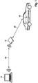
- FIG. 1 shows a typical system block diagram to illustrate the implementation of a vehicle diagnosis.
- the illustration shows a vehicle 10, a vehicle communication interface 12, which is also referred to herein as a VCI, and an external computing unit 14, typically a PC.
- VCI vehicle communication interface 12
- external computing unit 14 typically a PC.
- VCI 12 data can be exchanged with the vehicle 10 as part of an on-board diagnosis 20, with different vehicle diagnosis interfaces being used. Data are read out from the vehicle 10.
- the VCI 12 sends this data on to the processing unit 14, in which it is evaluated.
- An interface 24, for example USB or WiFi, is typically used to transmit the data between VCI 12 and processing unit 14.
- the computing unit 14 can, however, also be integrated in the overall system, for example as an embedded device.
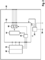
- FIG. 2 shows the structure and function of the presented vehicle communication interface with an integrated ASIC, which serves as an electronic unit of the type described.
- the illustration shows, in a greatly simplified block diagram, a vehicle communication interface 30, which is also referred to below as VCI.
- An electronic unit 32 is provided in this vehicle communication interface 30, which is typically designed as an ASIC.
- a power supply unit 34 is provided in the vehicle communication interface 30, which is connected to an external battery 36, which supplies, for example, 12 V supply voltage, and provides different supply voltages, for example 5 V, 10 V and 3.3 V.
- an interface controller 38 and / or a microcontroller 40 which can be implemented in an FPGA, are provided.
- the microcontroller 40 and the interface controller 38 can also be present as so-called stand-alone devices. Possible configurations are in Figure 7 shown.
- a transceiver array 44, a switch matrix 46 and a communication interface 48 with control and status registers are provided in the electronic unit.
- the transceiver array 44 and the communication interface 48 or the switching matrix 46 and the communication interface 48 can be provided in a separate electronic unit.
- the electronic unit 32 off Figure 2 which is also known as VCI-ASIC, can have a modular structure and can be accessed via the in Figure 3 modules shown.
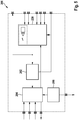
- Figure 3 shows an embodiment of the electronic unit with a computing unit 70, wherein alternatively an FPGA or an FPGA, which is arranged between the computing unit 70 and the VCI-ASIC, a switching matrix 72, a transceiver array 74, a Control / status register 76, an ADC with ADC multiplexer 82, a DLC communication buffer 84, a voltage monitor 86, a block 92 for the reset processing, a monitoring module 94 and a DLC connection 96 (DLC: diagnostic link connector).
- DLC diagnostic link connector
- the central elements of the VCI-ASIC are the switching matrix and the transceiver array.
- the switching matrix supports parallel communication and is designed in such a way that the output interface to the OBD connector is robust against reverse polarity and overvoltage as well as against high peak or peak voltages.
- the switching matrix is divided into different switching groups that support different requirements in terms of voltage capability, input and throughput capacitance and volume resistance.
- the switching matrix supports DolP (Diagnosis over IP), e.g. via an Ethernet interface in the vehicle.
- switches which are designed very special and complex, so that it is possible to connect the measurement technology with and without active communication with the vehicle at each pin, individually or in parallel.
- This option is currently not possible with switches that are usually discrete and requires larger, special optical switches and Relays with associated higher space requirements and higher costs.
- the reason for this is the low-leakage current switch required for the measurement technology, so that there can be no voltage measurements with a large measurement error on the ADC.
- the special ASIC switches are newly developed switches, derived from previously known ASIC switches from the medical field, with extremely small leakage currents and the additionally required negative voltage range for vehicle diagnostics.
- Diagnosis via communication can not only be carried out via the usual standard transceivers with the vehicle, but the communication itself can also be diagnosed using measurement technology in order to detect hardware errors within this diagnostic interface and diagnose them more precisely.
- the ADC described here with a multiplexer is used in conjunction with the switching matrix and the transceiver array.
- the switch consists, for example, of a back-to-back switch structure with two MOSFETs, as shown in FIG Figure 4 is shown. Such switches can be switched off in both directions, a parasitic current path is formed.
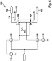
- Figure 4 shows a back-to-back switch structure with two MOSFETs, which is designated as a whole by the reference number 100.
- This comprises a first MOSFET 102 and a second MOSFET 104, a first switched current source 106, a second switched current source 108, a first voltage source 110 and a second voltage source 112.
- a first pin 120 and a second pin 122 are also shown.
- Communication can be bidirectional, ie in both directions. This means that both the first pin 120, can receive and send and, for example, is wired to DLC pins, and the second pin 122 can send and receive and is typically continued in the ASIC. This can then be routed to other internal switches or to a transceiver. Two directions of communication are therefore possible.
- the back-to-back switch structure 100 now makes it possible to selectively enable both communication directions 130 and 132 and also to switch off both communication directions 130 and 132 at one point in time, ie to suppress or deactivate the signal flow in both communication directions 130 and 132.
- the switch structure 100 is an example of a switch, at least one switch being provided according to claim 1.
- the switch can be an element, for example a logic, which regularly controls the two MOSFETs 102 and 104 separately, for example with a high or high level or a low or low level.
- the element can control the MOSFETs separately from one another, ie they can also control them control different signals.
- both communication directions 130 and 132 can optionally be enabled or both can be deactivated.
- the minimized leakage current is achieved through the use of a special gate-source control.
- This special control is characterized by the fact that it is controlled with a voltage or current source that is not referenced to ground.
- this consists, for example, of the two switched current sources 108, 110, which mutually compensate for the current through a gate-source resistor 114, so that there is no fault current through the back-to-back switch structure 100 with the two MOSFETs 102, 104 flows.
- the back-to-back switch structure is blocked with a high resistance by the gate-source resistor 114.
- the communication interface with control and status registers is discussed below:
- the ASIC is configured and controlled via a communication interface. Diagnosis is also possible via the interface. Measured values from the integrated measurement technology, ADC with multiplexer and measurement data processing, can also be obtained.
- FIG. 5 shows a module with ADC and ADC multiplexer, which is designated as a whole by the reference numeral 200.
- the illustration shows an ADC 202, a control logic 204, a reference voltage output 206 and an ADC multiplexer 208, which in this case comprises 32 channels.
- the ADC 202 can also be implemented externally. In this case, only the multiplexer would then be implemented in the ASIC.
- the ADC 202 supports the measurement of transceiver voltage signals as well as the measurement of external voltage signals, such as e.g. B. sensors and actuators.
- This integrated function block can be a Represent a unique selling point.
- the multiplexer currently supports a large number of analog and digital inputs.
- the measurement technology processing unit 204 stores the maximum, minimum and average values that have occurred for each channel over a set time range. The current measured value can also be read out from each channel independently of this.
- the ASIC offers outputs for external measurement technology with which it is possible to diagnose communication with a higher resolution, e.g. with oscilliscope functions. So z. B. CAN curves or messages are shown in more detail.
- FIG. 6 shows a DLC communication buffer module, which is designated as a whole by the reference numeral 250.
- This module 250 only represents an interface to lead the communication bus of the ASIC to external components.
- the illustration shows a first transceiver 252, a second transceiver 254, a third transceiver 256 and a fourth transceiver 258.
- the transceivers 252 to 258 are constructed identically. They are pure level converters with externally adjustable switching levels. Depending on the design of the communication bus, several transceivers can also be contained in the module 250.
- the VCI ASIC ensures that the entire VCI is always in a safe state. This creates the basis that the VCI can also be operated while a vehicle is in motion.
- the important interface controllers such as CAN, K-Line, etc.
- the interface controllers can also be implemented in the FPGA.
- a first embodiment 300 comprises an FPGA 302 and an ASIC 304.
- a processor 306 and one or more interface controllers 308 are provided in the FPGA 302.
- the interface controller or controllers 308 can support multiple interfaces such as CAN.
- a second embodiment 320 comprises a computing unit 322 with one or more interface controllers 324 and an ASIC 326.
- a third embodiment 340 comprises a computing unit 342, an FPGA 344 with one or more interface controllers 346 and an ASIC 348.
Landscapes
- Engineering & Computer Science (AREA)
- Physics & Mathematics (AREA)
- General Physics & Mathematics (AREA)
- Computer Networks & Wireless Communication (AREA)
- Signal Processing (AREA)
- Health & Medical Sciences (AREA)
- Computing Systems (AREA)
- General Health & Medical Sciences (AREA)
- Medical Informatics (AREA)
- General Engineering & Computer Science (AREA)
- Automation & Control Theory (AREA)
- Small-Scale Networks (AREA)
Description
- Die Erfindung betrifft eine elektronische Einheit für eine Fahrzeugkommunikationsschnittstelle und eine solche Fahrzeugkommunikationsschnittstelle.
- Eine Fahrzeugkommunikationsschnittstelle, die auch als VCI (Vehicle Communication Interface) bezeichnet wird, wird im Rahmen der Fahrzeugdiagnose eingesetzt. Darunter sind eine Reihe von technischen Verfahren und Anwendungen zu verstehen, die bspw. bei der Fehleranalyse bei Defekten, bei der Qualitätssicherung und bei der Fahrzeugentwicklung verwendet werden. Zum Datenaustausch mit dem Fahrzeug bzw. mit Komponenten im Fahrzeug werden Fahrzeugdiagnoseschnittstellen verwendet, die speziell für die Fahrzeugdiagnose ausgelegt sind. Diese Fahrzeugdiagnoseschnittstellen können unterschiedlich beschaffen sein. Es ist daher eine einheitliche Kommunikationsschnittstelle erforderlich, mit der die unterschiedlichen Fahrzeugdiagnoseschnittstellen angesteuert werden können.
- Hierzu werden seit einigen Jahren als VCIs bezeichnete Fahrzeugkommunikationsschnittstellen verwendet, die als Schnittstelle zwischen mindestens einer Fahrzeugdiagnoseschnittstelle und einer Recheneinheit, bspw. einem PC (PC: Personal Computer), zum Einsatz kommen. Die Fahrzeugdiagnoseschnittstelle im Fahrzeug ist wiederum mit den im Fahrzeug verbauten Steuergeräten verbunden. Hierbei kommen unterschiedliche Schnittstellen, wie bspw. High Speed CAN, Fault Tolerant CAN, Single Wire CAN, J1850 oder OEM-spezifische Schnittstellen zum Einsatz. CAN (CAN: Controller Area Network) ist ein serielles Bussystem. Als OEM (OEM: Original Equipment Manufacturer) wird ein Erstausrüster benannt. Die Anschluss- bzw. Pin-Belegung der Fahrzeugdiagnoseschnittstelle ist dabei definiert.
- Damit ist auch die Pin-Belegung am OBD-Stecker (OBD: On-board-Diagnose) im Fahrzeug definiert. Dennoch lässt die Schnittstellendefinition Optionen offen, die zu OEM-spezifischen Belegungen führen. Außerdem ist zu beachten, dass ältere Fahrzeuge ggf. über keinen OBD-Stecker, sondern über kundenspezifische Diagnosesteckverbinder verfügen.
- Das VCI enthält unterschiedliche Sendeempfänger bzw. Transceiver und Con- troller, um die voranstehend genannten Protokolle zu unterstützen. Des Weiteren können die unterschiedlichen Pins der Transceiver über eine sogenannte Schalt- bzw. Switch-Matrix auf viele Pins des OBD-Steckers geschaltet werden. Über spezifische Adapterkabel lässt sich das VCI auch mit anderen OEM-spezifischen Diagnoseschnittstellen verbinden.
- Es sind VCIs bekannt, die über einen Analog-Digital-Wandler bzw. ADC (ADC: Analog-to-Digital-Converter) verfügen, der u. a. die messtechnische Auswertung von Transceiver-Signalen ermöglicht. Damit können zusätzliche Diagnosefunktionen realisiert werden, bspw. eine Pegelüberprüfung von Signalen auf die korrekten High- und Low-Pegel. Ein High-Pegel ist in positiver Logik eine logische 1, ein Low-Pegel eine logische 0. Auf diese Weise ist eine weitreichendere bzw. tiefere Diagnose als mit der einfachen digitalen Auswertung der Transceiver-Signale möglich. Eine Früherkennung von hochohmigen Abschlusswiderständen oder Leitungen vor dem Totalausfall wird dadurch ebenso möglich.
- Aus der Druckschrift
EP 2259230 A1 ist beispielsweise ein programmierbares on-board Diagnosemodul für ein Fahrzeug bekannt, das ein elektronisches Konfigurationsarray umfasst. Letzteres umfasst selektive Verbindungsvorrichtungen, deren Betätigung zu einer Verbindung von Kommunikationspins eines Steuermoduls mit Verbindungspins eines Verbindungsanschlusses führt. Verschiedene Verbindungsarten zwischen den Pins sind dabei möglich. Die Pins sind für Datenempfang und -senden vorgesehen. Die Verbindungsvorrichtungen können Mikroschalter umfassen, die auf Befehl öffnen oder schließen. Der Konfigurationsarray ist als integrierter Schaltkreis (z.B. Mikrochip) ausgebildet. Jede der Verbindungsvorrichtungen ist normalerweise so geschaltet, dass eine Verbindung zwischen einem Kommunikationspin und einem oder mehreren Verbindungspins vorliegt. Ausgehend von diesem Schaltzustand wird in einer Öffnungsoperation die Verbindung zwischen den Pins unterbrochen. - Die Druckschrift
EP 2 302 597 A1 offenbart ein programmierbares Fahrzeugdiagnosesystem mit einem Diagnosegerät an Bord des Fahrzeugs und konfiguriert zur Erzeugung von Fahrzeugdaten über einen Diagnosekonnektor mit mehreren Pins zum Zugriff auf die Daten. Ferner mit einem Onboard Diagnosemodul zum Sammeln der Fahrzeugdaten mit einem Konnektor, der mehrere Pins aufweist und eingerichtet ist, um in einer stabilen aber leicht entfernbaren Weise mit dem Diagnosekonnektor verbunden zu werden. Ferner einer Steuereinheit mit mehreren Terminals zum Austausch von Fahrzeugdaten mit den Pins des Konnektors. Ferner einer elektronischen Schaltmatrix mit mehreren selektiven Zwischenverbindungsgeräten, die jeweils zur Verbindung jedes Konnektorpins mit jedem der Terminals der Steuereinheit betrieben werden können. Ferner einem externen Programmiersystem, das zur Steuerung der selektiven Schaltung der Zwischenverbindungsgeräte der elektronischen Schaltmatrix über das Onboard Diagnosemodul konfiguriert ist. - Aus der
US 2008/103652 A1 sind eine Vorrichtung und ein Verfahren bekannt, dieses einem Scan Tool ermöglichen, mit einem Datenverbindungskonnektor in einem Fahrzeug zu kommunizieren. Ein Kabel kann automatisch seine Verbindungen multiplexieren, um die geeigneten Verbindungen zwischen dem Scan Tool und dem Datenverbindungskonnektor basierend auf einem Kommunikationsprotokoll des getesteten Fahrzeugs herzustellen. Dies ermöglicht es dem Scan Tool mit dem Datenverbindungskonnektor zu kommunizieren ungeachtet der vom Kommunikationsprotokoll des Fahrzeugs verwendeten Pins. - Aus der
US2006217855A1 ist ein Fahrzeugdiagnoseschnittstellenadapter als integrierter Schaltkreis bekannt, der ein Halbleitersubstrat mit zwei integralen Gateway Konduktoren umfasst. Ein Satz paarweiser Schalter auf dem Substrat verbindet beliebige zwei Kontakte eines ersten Kontaktsatzes mit den Gateway Konduktoren. Ein anderer Satz paarweiser Schalter auf dem Substrat verbindet die zwei Gateway Konduktoren mit einem beliebigen Paar eines zweiten Kontaktsatzes entsprechend einem besonderen Fahrzeugnetzwerkkommunikationsprotokollschaltkreis in einem Fahrzeugdiagnosegerät. Beide Schaltsätze werden von einem integrierten Schaltsteuermodul gesteuert. - Die Druckschrift
US 2008/0004762 A1 beschreibt eine anwendungsspezifische integrierte Schaltung, die mit einem Fahrzeugdiagnosewerkzeug versehen ist. Die Schaltung umfasst ein Leistungsversorgungsmodul, eine Tastaturschnittstelle, einen Oszillator, einen Mikrocontroller, einen Datenverbindungscontroller, eine Fahrzeugschnittstelle, einen Anzeigecontroller und eine Speicherschnittstelle. - Aus der Druckschrift
CN 102591326 A ist ein Schnittstellenbaustein für die Fahrzeugdiagnose bekannt. Dieser Baustein umfasst eine Schalt-Matrix, ein Bus-Transceiver-Modul, ein Auswahlmodul für serielle Dateneingabekanäle und ein internes Leistungsversorgungs-Schaltkreismodul. - Die Schnittstelle zwischen dem PC und dem VCI kann drahtgebunden ausgeführt sein, bspw. mit einer USB-Schnittstelle (USB: Universal Serial Bus), einer seriellen Schnittstelle, oder drahtlos, bspw. BT (BT: Bluetooth), WLAN (WLAN: Wireless Local Area Network), ZigBee, ein Industriestandard für Funknetze, oder mit anderen Funkstandards, ausgeführt sein. Die auf dem angeschlossenen PC installierte Anwendungs- bzw. Applikations-Software kann das VCI konfigurieren und ruft über das VCI z. B. Diagnoseinformationen aus den Steuergeräten im Fahrzeug ab.
- Die heutigen VCIs verfügen dabei über eine diskret aufgebaute Schalt-Matrix sowie zum Teil diskret realisierte Transceiver. Grundsätzlich verfügen VCIs über weitere dargestellte Funktionsgruppen.
- Vor diesem Hintergrund werden eine elektronische Einheit mit den Merkmalen des Anspruchs 1 und eine Fahrzeugkommunikationsschnittstelle, ein VCI, gemäß Anspruch 12 vorgestellt. Ausführungen ergeben sich aus den abhängigen Ansprüchen.
- Die vorgestellte elektronische Einheit dient für eine Fahrzeugkommunikationsschnittstelle, welche für eine bidirektionale Kommunikation ausgelegt ist. Die elektronische Einheit umfasst eine Schalt-Matrix mit mindestens einem Schalter, der mit einem ersten Pin und einem zweiten Pin verbunden ist, wobei in einer ersten Kommunikationsrichtung der erste Pin sendet und der zweite Pin empfängt und in einer zweiten Kommunikationsrichtung der erste Pin empfängt und der zweite Pin sendet, wobei der mindestens eine Schalter dazu ausgelegt ist, beide Kommunikationsrichtungen gleichzeitig zu unterbrechen bzw. abzuschalten. Dabei ist die elektronische Einheit als integrierter Baustein ausgebildet. Wenigstens einer von dem mindestens einen Schalter kann als leckstromarmer Schalter ausgebildet sein. In einer Ausführung sind mehrere Schalter vorgesehen, die alle als leckstromarme Schalter ausgebildet sind. Weiterhin kann die elektronische Einheit ein Element zum Schalten des mindestens einen Schalters umfassen.
- Ist nur ein Schalter vorgesehen, so ist die Schaltmatrix als 1x1-Matrix ausgebildet. Sind bspw. vier Schalter vorgesehen, so ist die Schaltmatrix als 2x2- oder auch als 4x1-Schaltmatrix ausgebildet. Es sind unterschiedliche Anzahlen von Schaltern und verschiedene Schaltmatrizen denkbar.
- In einer Ausgestaltung ist die elektronische Einheit als anwendungsspezifische integrierte Schaltung bzw. als ASIC (ASIC: Application-Specific Integrated Circuit) ausgebildet sein. Die Verwendung eines ASICs ermöglicht eine auf die Anwendung ausgerichtete Struktur der elektronischen Einheit.
- Wenigstens einer von dem mindestens einen Schalter der Schalt-Matrix ist bspw. als Back-to-Back-Schalterstruktur ausgebildet. Sind mehrere Schalter vorgesehen, so kann weigstens einer der Schalter als Back-to-Back-Schalterstruktur ausgebildet sein. In Ausgestaltung sind alle Schalter mit einer Back-to-Back-Schalterstruktur ausgebildet. Es wird hierzu auf
Figur 4 verwiesen. Zu berücksichtigen ist, dass wenigstens einer von dem mindestens einen Schalter als leckstromarmer Schalter ausgebildet ist. Sind mehrere Schalter vorgesehen, so kann jeder Schalter als leckstromarmer Schalter ausgebildet sein. - Weiterhin kann eine Transceiver-Anordnung bzw. ein Transceiver-Array vorgesehen sein, das als Pegelwandler dient.
- In einer weiteren Ausgestaltung ist eine zusätzliche Recheneinheit vorgesehen ist, die als Master in der elektronischen Einheit dient. Die Master-Funktion weist auf eine hierarchische Struktur innerhalb der elektronischen Einheit hin. Der Master kontrolliert die anderen Komponenten, die auch als Slaves bezeichnet werden. Anstelle der Recheneinheit kann auch ein programmierbarer integrierter Schaltkreis bzw. ein FPGA (FPGA: Field Programmable Gate Array) verwendet werden.
- Es kann weiterhin zusätzlich eine weitere Kommunikationsschnittstelle vorgesehen sein, die u. a. zur Konfiguration der elektronischen Einheit dient.
- Weiterhin kann zusätzlich ein Modul mit ADC vorgesehen sein, wobei der ADC mit einem Multiplexer zusammenwirkt, um unterschiedliche Fahrzeugbusse ansprechen zu können.
- Es kann auch zusätzlich ein Modul mit ADC-Multiplexer vorgesehen sein, um die elektronische Einheit an unterschiedliche Fahrzeugbusse anzupassen. Bei dem Modul mit ADC-Multiplexer führt der Multiplexer mehrere Signale auf einen ADC-Eingang.
- In einer weiteren Ausführungsform ist zusätzlich ein Überwachungsmodul vorgesehen, das zur Kontrolle des Masters dient.
- Es kann außerdem zusätzlich eine Spannungsüberwachung vorgesehen sein, die zur Überwachung von externen Spannungen dient.
- Es wird weiterhin eine Fahrzeugkommunikationsschnittstelle zum Anschließen an eine Fahrzeugdiagnoseschnittstelle vorgestellt, über die eine Fahrzeugdiagnose durchgeführt werden kann. Diese umfasst eine elektronische Einheit der vorstehend beschriebenen Art.
- Die vorgestellte elektronische Einheit für eine Fahrzeugkommunikationsschnittstelle kann in einer Ausgestaltung somit folgende Blöcke bzw. Module umfassen:
- Schalt-Matrix mit Schalter, die in Ausgestaltung sehr geringe Leckströme aufweisen und für eine hohe Impedanz gestaltet sind und an eine präzise analoge Messeinrichtung angebunden sind, der Schalt-Matrixbetrieb ist für einen großen negativen und positiven Eingangsspannungsbereich ausgelegt, d. h. es ist die Möglichkeit gegeben, Kommunikationssignale auf verschiedene DLC-Pins (DLC: Data Link Connector) schalten zu können; damit können verschiedene herstellerspezifische Kommunikationsarten unterstützt werden,
- Transceiver-Anordnung, diese dient als Schnittstelle bzw. Interface, die bzw. das Controllersignale in protokollspezifische Signale wandelt und somit einen Pegelwandler darstellt,
- Kommunikationsschnittstelle mit Steuer- und Statusregister, diese dient zur Konfiguration der elektronischen Einheit, bspw. eines ASICs wie auch zur Diagnose, insbesondere zur Fehlerdiagnose, und zur Fehlerbehandlung,
- ADC mit Multiplexer, der ADC wird verwendet, um Diagnosen auf verschiedenen Fahrzeugbussen durchzuführen, damit kann jeder Pin bedient werden,
- Analog-Multiplexer, dieser ist vor dem ADC angeordnet, damit der ADC auf jeden DLC-Pin über den Multiplexer schalten kann, um Signal herunterzuteilen, den Spannungseingangsbereich bzw. Messbereich zu variiere, der ADC-Multiplexer ist deaktivierbar, um hochgenaue Spannungsmessungen zu ermöglichen,
- autonome Steuereinheit mit Zustandsmaschinen für ADC Messdatenverarbeitung zum Ausschalten bzw. Entlasten eines externen Sternverteilers bzw. MCU (MCU: Multipoint Control Unit), diese ist dazu ausgelegt, zyklisch, zeitsynchron oder auch winkelsynchron Spannungssignale auf DLC-Pins zu erfassen, weiterhin diese Steuereinheit eine Abtastung bzw. ein Sampling der ADC-Messwerte automatisch durch, es ist kein zusätzlicher Aufwand durch den Einsatz von Software erforderlich um dies zu triggern,
- DLC-Kommunikations-Puffer bzw. -Buffer, dieser dient der Zwischenspeicherung von Daten, insbesondere von ADC-Daten oder Kommunikationsdaten,
- Spannungsüberwachung von externen Spannungen, diese wird dazu eingesetzt, bei Spannungsunterschreitung den ASIC in den Grundzustand bzw. den default-Zustand zurückzusetzen, dabei werden die Schalter auf dem SPI-Register zurückgesetzt,
- Rücksetz-Verarbeitung mit einem sogenannten Rücksetz- bzw. Reset-Modul, mit diesem wird eine Systemspannung des VCI überwacht, bei Unterschreitung wird ein RESET generiert, dies kann auf FPGA geführt werden, das den VCI wiederum zurücksetzt,
- Überwachungseinheit, diese ermöglicht es, durch ein zyklisches Frage-Antwort Spiel die Funktion des Masters, eines Rechner oder FPGA, im Gesamtsystem zu verifizieren, es besteht eine Verbindung zur Rücksetzverarbeitung, diese wird bei Überschreiten eines Fehlerzählers getriggert.
- Die vorgestellte Hardware stellt eine rückwärtskompatible Lösung für bereits verfügbare diskrete Realisierung der voranstehend genannten Hardware-Module dar.
- Die vorgestellte elektronische Einheit im VCI, die bspw. in einem ASIC implementiert ist, kann vielfältig verwendet werden. Neben der analogen Spannungsmessung, die eine umfangreiche Diagnose des Bussystems ermöglicht, eröffnet die elektronische Einheit bzw. das VCI-ASIC folgende Potentiale bzw. Möglichkeiten und umfasst folgende Funktionalitäten:
- 1. Darstellung einer kostengünstigen Hardware-Lösung für VCIs durch Reduzierung des Leiterplattenflächenbedarfs.
- 2. Das VCI-ASIC unterstützt eine parallele Kommunikation. Das bedeutet, dass viele unterschiedliche Fahrzeugschnittstellen parallel über den OBD-Stecker bedient werden können. Diese Funktionalität unterstützt schnellere Fahrzeugdiagnosezeiten sowie Programmierzeiten.
- 3. Eine weitere hervorzuhebende Funktionalität ist die Integration einer Messtechnikfunktionalität in dem System-ASIC. Mit dieser Messtechnik kann eine analoge Messung von externen Signalen, z. B. CAN-Signalen, erfolgen.
- 4. Ein weiteres Merkmal des VCI-ASICs besteht darin, dass digitale Sensoren und Aktoren über das Messtechnikmodul diagnostiziert werden können.
- 5. Ein weiteres Merkmal ist die verfügbare Abdeckung des ASICs, um über die OBD-spezifizierten Diagnosemöglichkeiten hinaus alle bisher bekannten Diagnosemöglichkeiten aller Fahrzeuge aller Hersteller abzudecken.
- 6. Die bisher bekannten ASIC-Lösungen verarbeiten nur negative Eingangssignale bis -2 V, das vorgestellte VCI-ASIC verarbeitet negative Spannungen bis zur vollen CAN-Konformität. CAN-Konformität bedeutet dabei die Einhaltung einer Norm, die zwei Schichten, nämlich die physikalische Schicht bzw. physical layer und die Protokollschicht bzw. protocol layer, des OSI-Schichtenmodells der verwendeten Netzwerkprotokolle beschreibt. Das OSI-Schichtenmodell (OSI: Open Systems Interconnection Model) ist ein Referenzmodell für Netzwerkprotokolle als Schichtenarchitektur. Das OSI-Schichtenmodell ermöglicht eine Kommunikation über unterschiedliche technische Systeme hinweg. Hierzu definiert das Modell sieben aufeinanderfolgende Schichten, denen jeweils eng begrenzte Aufgaben zugeordnet sind.
- Weitere Vorteile und Ausgestaltungen der Erfindung ergeben sich aus der Beschreibung und den beiliegenden Zeichnungen.
- Es versteht sich, dass die voranstehend genannten und die nachstehend noch zu erläuternden Merkmale nicht nur in der jeweils angegebenen Kombination, sondern auch in anderen Kombinationen oder in Alleinstellung verwendbar sind, ohne den Rahmen der vorliegenden Erfindung zu verlassen.
-
- Figur 1
- zeigt in Übersichtsdarstellung ein Systemblockschaltbild.
- Figur 2
- zeigt eine Ausführungsform der vorgestellten Fahrzeugkommunikationsschnittstelle.
- Figur 3
- zeigt eine Ausführungsform eines VCI-ASIC, der als elektronische Einheit dient.
- Figur 4
- zeigt eine Back-to-Back Schalterstruktur.
- Figur 5
- zeigt in einem Blockschaltbild einen ADC und einen ADC-Multiplexer.
- Figur 6
- zeigt in einem Blockschaltbild einen DLC-SPI-Buffer (DLC: data link control; SPI: Serial Peripheral Interface)
- Figur 7
- zeigt mögliche Konfigurationen der Fahrzeugkommunikationsschnittstelle.
- Die Erfindung ist anhand von Ausführungsformen in den Zeichnungen schematisch dargestellt und wird nachfolgend unter Bezugnahme auf die Zeichnungen ausführlich beschrieben.
-
Figur 1 zeigt ein typisches Systemblockschaltbild zur Verdeutlichung der Durchführung einer Fahrzeugdiagnose. Die Darstellung zeigt ein Fahrzeug 10, eine Fahrzeugkommunikationsschnittstelle 12, die hierin auch als VCI bezeichnet wird, sowie eine externe Recheneinheit 14, typischerweise einen PC. - Mit dem VCI 12 können im Rahmen einer On-board-Diagnose 20 Daten mit den Fahrzeug 10 ausgetauscht werden, wobei unterschiedliche Fahrzeugdiagnoseschnittstellen verwendet werden. Daten werden aus dem Fahrzeug 10 ausgelesen. Das VCI 12 sendet diese Daten weiter an die Recheneinheit 14, in der diese ausgewertet werden. Zum Übertragen der Daten zwischen VCI 12 und Recheneinheit 14 kommt typischerweise eine Schnittstelle 24, bspw. USB oder WiFi, zum Einsatz. Die Recheneinheit 14 kann aber auch im Gesamtsystem, bspw. als eingebettetes bzw. embedded Gerät, integriert sein.
-
Figur 2 zeigt den Aufbau und die Funktion der vorgestellten Fahrzeugkommunikationsschnittstelle mit einem integrierten ASIC, der als elektronische Einheit der beschriebenen Art dient. - Die Darstellung zeigt in einem stark vereinfachten Blockschaltbild eine Fahrzeugkommunikationsschnittstelle 30, die nachstehend auch als VCI bezeichnet wird. In dieser Fahrzeugkommunikationsschnittstelle 30 ist eine elektronische Einheit 32 vorgesehen, die typischerweise als ASIC ausgebildet ist. Weiterhin ist in der Fahrzeugkommunikationsschnittstelle 30 eine Leistungsversorgungseinheit 34 vorgesehen, die mit einer externen Batterie 36, die bspw. 12 V Versorgungsspannung liefert, verbunden ist und unterschiedliche Versorgungsspannungen, bspw. 5 V, 10 V und 3,3 V, bereitstellt. Weiterhin sind ein Schnittstellen-Controller 38 und/oder ein Mikrocontroller 40, der in einem FPGA implementiert sein kann, vorgesehen. Der Mikrocontroller 40 und der Schnittstellen-Controller 38 können auch als sogenannte Stand-Alone Devices vorhanden sein. Mögliche Konfigurationen sind in
Figur 7 gezeigt. - In der elektronischen Einheit sind ein Transceiver-Array 44, eine Schalt-Matrix 46 und eine Kommunikationsschnittstelle 48 mit Steuer- und Status-Register vorgesehen. Das Transceiver-Array 44 und die Kommunikationsschnittstelle 48 bzw. die Schalt-Matrix 46 und die Kommunikationsschnittstelle 48 können in einer separaten elektronischen Einheit vorgesehen sein.
- Die elektronische Einheit 32 aus
Figur 2 , die auch als VCI-ASIC bezeichnet wird, kann modular aufgebaut sein und über die inFigur 3 dargestellten Modulen verfügen.Figur 3 zeigt eine Ausführung der elektronischen Einheit mit einer Recheneinheit 70, wobei alternativ ein FPGA bzw. ein FPGA, das zwischen der Recheneinheit 70 und dem VCI-ASIC angeordnet ist, vorgesehen sein kann, einer Schalt-Matrix 72, einem Transceiver-Array 74, einem Steuer/Status-Register 76, einem ADC mit ADC-Multiplexer 82, einem DLC-Kommunikations-Buffer 84, einer Spannungsüberwachung 86, einem Block 92 für die Rücksetz-Verarbeitung, einem Überwachungsmodul 94 und einem DLC-Anschluss 96 (DLC: diagnostic link connector). - Im Folgenden werden die Module anhand ihrer Funktionalitäten näher erläutert.
- Die zentralen Elemente des VCI-ASICs sind in Ausgestaltung die Schalt-Matrix und das Transceiver-Array. Die Schalt-Matrix unterstützt eine parallele Kommunikation und ist derart gestaltet, dass die Ausgangsschnittstelle zum OBD-Stecker robust gegen Spannungsverpolung und Überspannung sowie gegenüber hohen Spitzen- bzw. Peakspannungen ausgelegt ist. Die Schalt-Matrix ist in verschiedene Schalt-Gruppen unterteilt, die unterschiedliche Anforderungen hinsichtlich der Spannungsfähigkeit, Eingangs- und Durchgangskapazität sowie Durchgangswiderstand unterstützen. Zudem unterstützt die Schalt-Matrix DolP (Diagnosis over IP) bspw. mittels Ethernet-Schnittstelle im Fahrzeug.
- Ein in einer Ausführung wichtiges Merkmal ist der Aufbau der Schalter, die sehr speziell und aufwendig gestaltet sind, so dass es möglich ist, die Messtechnik mit und ohne aktive Kommunikation mit dem Fahrzeug an jedem Pin, einzeln oder parallel, aufzuschalten. Diese Option ist derzeit mit gewöhnlich diskret aufgebauten Schaltern nicht möglich und bedarf größere spezielle optische Schalter und Relais mit verbundenem höheren Platzbedarf und höheren Kosten. Hintergrund sind die für die Messtechnik benötigten leckstromarmen Schalter, damit es zu keinen Spannungsmessungen mit einem großen Messfehler am ADC kommen kann. Die speziellen ASIC-Schalter sind neu entwickelte Schalter, abgeleitet aus bisher bekannten ASIC-Schaltern aus dem Medizinbereich, mit äußerst kleinen Leckströmen und dem zusätzlich benötigten negativen Spannungsbereich für die Fahrzeugdiagnose.
- Es kann eine Diagnose per Kommunikation nicht nur über die üblichen Standard-Transceiver mit dem Fahrzeug durchgeführt werden, sondern auch die Kommunikation selbst per Messtechnik diagnostiziert werden, um Hardware-Fehler innerhalb dieser Diagnoseschnittstelle zu erkennen und genauer zu diagnostizieren. Dazu wird der hierin beschriebene ADC mit Multiplexer im Zusammenspiel mit der Schalt-Matrix und dem Transceiver-Array verwendet.
- Es wird eine interne programmierbare Zustandsmaschine bzw. statemachine verwendet, um die Spannungen an DLC-Pins zyklisch messen zu können. Folgende Fehlerfälle können dabei über die Spannungsmessung mit dem ADC diagnostiziert werden:
- Kurzschluss nach Fahrzeugmasse oder zu einer anderen Spannungsquelle im Kabelbaum des Fahrzeugs,
- Lastabfall bzw. Open Load in der Zuleitung des VCIs zum Fahrzeug,
- Open Load am externen Kabelbaum des Fahrzeugs,
- genaue analoge Messung der High- und Low Pegel von Signalen während der Kommunikation, um Über- bzw. Unterschreitungen der zulässigen Grenzen zu erkennen.
- Für die Open-Load-Messungen mit einer integrierten Messtechnik sind hohe Eingangswiderstände der ADC-Messschaltung notwendig. Ein Leckstrom der Schalter in der Switch-Matrix von bspw. 1 µA würde über diesem Widerstand eine Messwertverfälschung von 1 V verursachen. Das ist für die Open-Load-Diagnose nicht verwendbar. Es ist eine sehr viel höhere Genauigkeit vom Messbereichsendwert erforderlich.
- Somit ist diese Open-Load-Diagnose nur möglich, wenn neben dem hohen Ausgangswiderstand des ASICs dieser über sehr kleine Leckströme, nämlich wenige nA, bei geöffneten oder geschlossenen Schaltern in der Schalt-Matrix verfügt. Der Schalter besteht bspw. aus einer Back-to-Back Schalterstruktur mit zwei MOSFETs, wie dies in
Figur 4 dargestellt ist. Derartige Schalter sind in beide Richtungen abschaltbar, es bildet sich ein parasitärer Strompfad. -
Figur 4 zeigt eine Back-to-Back-Schalterstruktur mit zwei MOSFETs, die insgesamt mit der Bezugsziffer 100 bezeichnet ist. Diese umfasst einen ersten MOSFET 102 und einen zweiten MOSFET 104, eine erste geschaltete Stromquelle 106, eine zweite geschaltete Stromquelle 108, eine erste Spannungsquelle 110 und eine zweite Spannungsquelle 112. Weiterhin sind ein erster Pin 120 und ein zweiter Pin 122 dargestellt. Eine Kommunikation kann bidirektion, d. h. in beide Richtungen, erfolgen. Dies bedeutet dass sowohl der erste Pin 120, empfangen und senden kann und bspw. mit DLC-Pins verdrahtet ist als auch der zweite Pin 122 senden und empfangen kann und typischerweise im ASIC weitergeführt wird. Dieser kann dann auf weitere interne Schalter oder auf einen Transceiver geführt werden. Es sind somit zwei Kommunikationsrichtungen möglich. In einer ersten Kommunikationsrichtung 130 sendet der erste Pin 120 und der zweite Pin 122 empfängt, in einer zweiten Kommunikationsrichtung 132 empfängt der erste Pin 120 und der zweite Pin 122 sendet. Die Back-to-Back-Schalterstruktur 100 ermöglicht es nun, beide Kommunikationsrichtungen 130 und 132 wahlweise zu ermöglichen und zu einem Zeitpunkt auch beide Kommunikationsrichtungen 130 und 132 abzuschalten, d. h. den Signalfluss in beide Kommunikationsrichtungen 130 und 132 zu unterdrücken bzw. zu deaktivieren. Die Schalterstruktur 100 ist ein Beispiel für einen Schalter, wobei gemäß Anspruch 1 mindestens ein Schalter vorgesehen ist. Ist ein Element zum Schalten dieses Schalters vorgesehen, so kann dieses, wenn der Schalter, wie bei der beschriebenen Ausführungsform als Back-to-Back-Schalterstruktur 100 mit den beiden MOSFETs 102 und 104 ausgebildet ist, eine Element sein, bspw. eine Logik, die die beiden MOSFETs 102 und 104 regelmäßig getrennt ansteuert, bspw. mit einem Hoch- bzw. High-Pegel oder einem Niedrig- bzw. Low-Pegel. Das Element kann die MOSFETs getrennt voneinander ansteuern, d. h. diese mit unterschiedlichen Signalen ansteuern. So können beide Kommunikationsrichtungen 130 und 132 wahlweise ermöglicht werden oder auch beide deaktiviert werden. - Der minimierte Leckstrom wird durch den Einsatz einer speziellen Gate-Source-Ansteuerung erreicht. Diese spezielle Ansteuerung zeichnet sich dadurch aus, dass mit einer nicht massebezogenen Spannungs- oder Stromquelle angesteuert wird. Im eingeschalteten Zustand besteht bspw. diese aus den zwei geschalteten Stromquellen 108, 110, die den Strom durch einen Gate-Source-Widerstand 114 gegenseitig kompensieren, so dass kein Fehlerstrom über die Back-to-Back Schalterstruktur 100 mit den beiden MOSFETs 102, 104 fließt. Im ausgeschalteten Zustand wird die Back-to-Back Schalterstruktur durch den Gate-Source-Widerstand 114 hochohmig gesperrt.
- Nachfolgend wird auf die Kommunikationsschnittstelle mit Steuer- und StatusRegister eingegangen:
Über eine Kommunikationsschnittstelle wird der ASIC konfiguriert und angesteuert. Zudem ist über die Schnittstelle eine Diagnose möglich. Ebenso können Messwerte der integrierten Messtechnik, ADC mit Multiplexer und Messdaten-Aufbereitung, erhalten werden. -
Figur 5 zeigt ein Modul mit ADC und ADC-Multiplexer, das insgesamt mit der Bezugsziffer 200 bezeichnet ist. Die Darstellung zeigt einen ADC 202, eine Steuerlogik 204, einen Referenzspannungsausgang 206 und einen ADC-Multiplexer 208, der in diesem Fall 32 Kanäle umfasst. Der ADC 202 kann auch extern realisiert sein. In diesem Fall wäre dann lediglich der Multiplexer im ASIC realisiert. - Der ADC 202 unterstützt die Messung von Transceiver-Spannungssignalen sowie die Messung von externen Spannungssignalen, wie z. B. von Sensoren und Aktoren.
- Des Weiteren sollen Signale von digitalen Sensoren analysiert und ausgewertet werden können. Die Auswertung digitaler Sensorsignale im VCI-ASIC spart somit Rechnerressourcen und somit Kosten. Dieser integrierte Funktionsblock kann ein Alleinstellungsmerkmal darstellen. Der Multiplexer unterstützt derzeit eine Vielzahl von analogen und digitalen Eingängen.
- Grundleistungsmerkmale des ADC 202 bei dieser Ausführung sind:
- mindestens 8-Bit Auflösung,
- ADC-Eingangsspannung mit einer Referenzspannung,
- minimale Abtastrate 10 ks/s,
- Grundleistungsmerkamle des Multiplexer 208 bei dieser Ausführung sind:
- n/1 Multiplexer,
- gepufferter Spannungsteiler mit einer Anzahl Eingangsinputs mit Anpassung des Spannungsbereichs und einer Toleranz von mindestens kleiner als 1 %,
- Grundleistungsmerkmale für den Referenzspannungsausgang 206 bei dieser Ausführung sind:
- etwa 5 V,
- Toleranz: +- 1%,
- Ausgangsstrom 1 mA.
- Die Messtechnik-Verarbeitungseinheit 204 speichert über einen eingestellten Zeitbereich für jeden Kanal jeweils den aufgetretenen Maximal-, Minimal- und Durchschnittswert. Ebenso kann unabhängig davon der aktuelle Messwert von jedem Kanal ausgelesen werden.
- Zusätzlich zur eingebauten Messtechnik-Verarbeitungseinheit bietet das ASIC Ausgänge für eine externe Messtechnik, mit der es möglich ist, die Kommunikation mit einer höheren Auflösung zu diagnostizieren, bspw. mit Oszilliskop-Funktionen. So können z. B. CAN-Kurven bzw. Nachrichten detaillierter dargestellt werden.
-
Figur 6 zeigt ein DLC-Kommunikations-Buffer-Modul, das insgesamt mit dem Bezugszeichen 250 bezeichnet ist. Dieses Modul 250 stellt lediglich eine Schnittstelle dar, um den Kommunikations-Bus des ASICs auf externe Komponenten zu führen. Die Darstellung zeigt einen ersten Transceiver 252, einen zweiten Transceiver 254, einen dritten Transceiver 256 und einen vierten Transceiver 258. Die Transceiver 252 bis 258 sind identisch aufgebaut. Es handelt sich um reine Pegelumsetzer mit extern einstellbaren Schaltpegeln. Es können je nach Ausführung des Kommunikations-Busses noch mehrere Transceiver im Modul 250 enthalten sein. - Nachstehend wird auf die Rücksetz-Verarbeitung und Überwachung eingegangen:
Das VCI-ASIC verfügt zudem über eine interne Rücksetz-Verarbeitung bzw. einen internen Reset Handler, die externe Versorgungsspannungen des gesamten VCI überwacht. Bei einer Unterschreitung oder Überschreitung von Grenzwerten für verschiedene Versorgungsspannungen werden RESET-Signale aktiviert, welche das System in einem sicheren Zustand halten. Auch verfügt das VCI-ASIC über ein Überwachungsmodul bzw. Monitoring Modul, welches den Rechnerkern oder ein FPGA überwachen kann. Im Rahmen der Überwachung dient das Überwachungsmodul als eine Art Master, bspw. eine Recheneinheit oder ein FPGA, der das VCI kontrolliert. Dies erfolgt bspw. durch ein Frage-Antwort-Spiel. Weiterhin besteht eine Verbindung zum Reset-Modul, um ggf. ein Rücksetzen auszulösen. Die Funktionalität des Monitoring-Moduls ist wie folgt: - Überwachung kann über ein Kommando aktiviert werden,
- Überwachung arbeitet unabhängig von µC- oder FPGA- Funktionalitäten im VCI,
- zyklische Überwachung über das Kommunikations-Modul muss gewährleistet sein,
- CRC-Berechnung im VCI-ASIC gewährleistet sichere Kommunikation (CRC: cyclic redundancy check),
- Watch-Dog VCI ASIC Pin signalisiert CRC Fehler bei SPI Kommunikation oder einen zyklische Monitoringfehler,
- Überwachungsmodul generiert Frage-/Antwortspiel, das vom µC oder FPGA in einem definierten Zeitfenster "richtig" beantwortet werden muss, bspw. über SPI oder eine parallele Schnittstelle.
- Im Zusammenspiel mit der Spannungsüberwachung durch das Reset-Handling-Modul stellt das VCI ASIC sicher, dass das gesamte VCI sich immer im sicheren Zustand befindet. Somit ist die Grundlage geschaffen, dass das VCI auch im Fahrbetrieb eines Fahrzeuges betrieben werden kann.
- Grundsätzlich werden die wichtigen Schnittstellen-Controller, wie bspw. CAN, K-Line usw., durch den Mikrocontroller unterstützt. Die Schnittstellen-Controller können auch im FPGA implementiert werden.
-
Figur 7 zeigt mögliche Konfigurationen der Fahrzeugkommunikationsschnittstelle. Eine erste Ausführung 300 umfasst ein FPGA 302 und ein ASIC 304. In dem FPGA 302 sind ein Prozessor 306 und ein oder mehrere Schnittstellen-Controller 308 vorgesehen. Der bzw. die Schnittstellen-Controller 308 kann bzw. können mehrere Schnittstellen, wie bspw. CAN, unterstützen. - Eine zweite Ausführung 320 umfasst eine Recheneinheit 322 mit einem oder mehreren Schnittstellen-Controllern 324 und ein ASIC 326. Eine dritte Ausführung 340 umfasst eine Recheneinheit 342, ein FPGA 344 mit einem oder mehreren Schnittstellen-Controllern 346 und ein ASIC 348.
Claims (12)
- Elektronische Einheit für eine Fahrzeugkommunikationsschnittstelle (12, 30, 300, 320, 340), welche für eine bidirektionale Kommunikation ausgelegt ist, mit einer Schalt-Matrix (46, 72) mit mindestens einem Schalter, der mit einem ersten Pin (120) und einem zweiten Pin (122) verbunden ist, wobei in einer ersten Kommunikationsrichtung (130) der erste Pin (120) sendet und der zweite Pin (122) empfängt und in einer zweiten Kommunikationsrichtung (132) der erste Pin (120) empfängt und der zweite Pin (122) sendet, wobei der mindestens eine Schalter dazu ausgelegt ist, beide Kommunikationsrichtungen (130 und 132) gleichzeitig zu unterbrechen, dadurch gekennzeichnet, dass zur Spannungsmessung eine Messschaltung mit einem Analog-Digital-Wandler (202) vorgesehen ist, wobei der Analog-Digital-Wandier (202) hohe Eingangswiderstände aufweist und wobei die elektronische Einheit (32) als integrierter Baustein mit sehr kleinen Leckströmen, nämlich wenigen nA, bei geöffneten oder geschlossenen Schaltern in der Schalt-Matrix (46, 72) ausgebildet ist, um eine Open-Load-Diagnose zu ermöglichen.
- Elektronische Einheit nach Anspruch 1, bei der wenigstens einer von dem mindestens einen Schalter als leckstromarmer Schalter ausgebildet ist.
- Elektronische Einheit nach Anspruch 1 oder 2, die als ASIC ausgebildet ist.
- Elektronische Einheit nach einem der Ansprüche 1 bis 3, bei dem wenigstens einer von dem mindestens einen Schalter der Schalt-Matrix als Back-to- Back-Schalterstruktur (100) ausgebildet ist.
- Elektronische Einheit nach einem der Ansprüche 1 bis 4, bei der ein Transceiver-Array (44, 74) vorgesehen ist, das als Pegelwandler dient.
- Elektronische Einheit nach einem der Ansprüche 1 bis 5, bei der eine zusätzliche Recheneinheit (70) vorgesehen ist, die als Master in der elektronischen Einheit dient.
- Elektronische Einheit nach einem der Ansprüche 1 bis 6, bei der zusätzlich eine weitere Kommunikationsschnittstelle (48) vorgesehen ist, die zur Konfiguration der elektronischen Einheit dient.
- Elektronische Einheit nach einem der Ansprüche 1 bis 7, bei der zusätzlich ein Modul mit ADC (202) vorgesehen ist, wobei der ADC (202) mit einem Multiplexer zusammenwirkt, um unterschiedliche Fahrzeugbusse ansprechen zu können.
- Elektronische Einheit nach einem der Ansprüche 1 bis 7, bei der zusätzlich ein Modul mit ADC-Multiplexer (208) vorgesehen ist, um die elektronische Einheit an unterschiedliche Fahrzeugbusse anzupassen.
- Elektronische Einheit nach einem der Ansprüche 1 bis 9, bei der zusätzlich ein Überwachungsmodul (94) vorgesehen ist zur Kontrolle eines Masters.
- Elektronische Einheit nach einem der Ansprüche 1 bis 10, bei der zusätzlich eine Spannungsüberwachung (86) vorgesehen ist, die zur Überwachung von externen Spannungen dient.
- Fahrzeugkommunikationsschnittstelle zum Anschließen an eine Fahrzeugdiagnoseschnittstelle, über die eine Fahrzeugdiagnose durchgeführt werden kann, wobei die Fahrzeugkommunikationsschnittstelle eine elektronische Einheit (32) nach einem der Ansprüche 1 bis 11 umfasst.
Applications Claiming Priority (2)
| Application Number | Priority Date | Filing Date | Title |
|---|---|---|---|
| DE102014204128.7A DE102014204128A1 (de) | 2014-03-06 | 2014-03-06 | Elektronische Einheit für eine Fahrzeugkommunikationsschnittstelle |
| PCT/EP2015/051485 WO2015132017A1 (de) | 2014-03-06 | 2015-01-26 | Elektronische einheit für eine fahrzeugkommunikationsschnittstelle |
Publications (2)
| Publication Number | Publication Date |
|---|---|
| EP3114652A1 EP3114652A1 (de) | 2017-01-11 |
| EP3114652B1 true EP3114652B1 (de) | 2020-12-02 |
Family
ID=52444283
Family Applications (1)
| Application Number | Title | Priority Date | Filing Date |
|---|---|---|---|
| EP15702211.2A Active EP3114652B1 (de) | 2014-03-06 | 2015-01-26 | Elektronische einheit für eine fahrzeugkommunikationsschnittstelle |
Country Status (5)
| Country | Link |
|---|---|
| US (1) | US10438423B2 (de) |
| EP (1) | EP3114652B1 (de) |
| CN (1) | CN106062829B (de) |
| DE (1) | DE102014204128A1 (de) |
| WO (1) | WO2015132017A1 (de) |
Cited By (1)
| Publication number | Priority date | Publication date | Assignee | Title |
|---|---|---|---|---|
| DE102022131564A1 (de) | 2022-11-29 | 2024-05-29 | Valeo Schalter Und Sensoren Gmbh | Steuervorrichtung für ein Zonensteuergerät, Zonensteuergerät und Verfahren zum Betreiben eines Zonensteuergeräts |
Families Citing this family (24)
| Publication number | Priority date | Publication date | Assignee | Title |
|---|---|---|---|---|
| DE102014204128A1 (de) * | 2014-03-06 | 2015-09-10 | Robert Bosch Gmbh | Elektronische Einheit für eine Fahrzeugkommunikationsschnittstelle |
| DE102014210238A1 (de) * | 2014-05-28 | 2015-12-03 | Robert Bosch Gmbh | Fahrzeugdiagnosevorrichtung |
| EP2988420B1 (de) * | 2014-08-20 | 2021-03-10 | Framatome | Schaltungsanordnung für ein sicherheits-i&c-system |
| DE102016208937A1 (de) * | 2016-05-24 | 2017-11-30 | Robert Bosch Gmbh | Kraftfahrzeug-Schnittstelleninterface |
| WO2018059686A1 (en) | 2016-09-29 | 2018-04-05 | Volvo Truck Corporation | An electronic control unit for a vehicle capable of controlling multiple electrical loads |
| US20180225249A1 (en) * | 2017-02-08 | 2018-08-09 | Automatic Labs, Inc. | Application-specific integrated circuit configured to interface with automotive diagnostic port |
| DE102017206559A1 (de) * | 2017-04-19 | 2018-10-25 | Robert Bosch Gmbh | Steuergerät und Betriebsverfahren hierfür |
| US10686623B2 (en) * | 2017-10-27 | 2020-06-16 | Bendix Commercial Vehichle Systems Llc | System and method for dynamic bi-directional communication over a local interconnect network bus |
| CN108303964B (zh) * | 2017-12-28 | 2020-09-11 | 深圳市元征科技股份有限公司 | 一种网络连接器及车辆诊断方法 |
| CN108255160B (zh) * | 2018-03-12 | 2023-09-08 | 深圳市博诺技术有限公司 | 一种38pin接口的汽车总线通信选线系统及方法 |
| US11023249B1 (en) * | 2018-09-26 | 2021-06-01 | United States Of America As Represented By The Administrator Of Nasa | First stage bootloader (FSBL) |
| EP3680955B1 (de) * | 2019-01-08 | 2023-08-16 | Samsung SDI Co., Ltd. | Batteriesystem |
| US11042129B2 (en) * | 2019-06-05 | 2021-06-22 | Control Dynamics, Inc. | Redundant wireless safety system for manufacturing environment |
| JP7135211B2 (ja) * | 2019-06-24 | 2022-09-12 | 日立Astemo株式会社 | 車載制御装置 |
| CN112241155A (zh) * | 2019-07-16 | 2021-01-19 | 深圳市道通科技股份有限公司 | 接口转换器及汽车诊断系统 |
| CN110519144B (zh) | 2019-09-20 | 2021-10-15 | 深圳市道通合创新能源有限公司 | 一种汽车诊断设备与车辆建立通信的方法、装置及汽车通信接口设备 |
| CN110794808A (zh) * | 2019-10-22 | 2020-02-14 | 深圳市朗仁科技有限公司 | 矩阵驱动装置及其多通道信号切换方法 |
| JP7097347B2 (ja) * | 2019-12-25 | 2022-07-07 | 本田技研工業株式会社 | 不正診断機検出装置 |
| US11249684B2 (en) * | 2020-05-22 | 2022-02-15 | Raytheon Company | Computation of solution to sparse matrix |
| CN113242532B (zh) * | 2021-05-12 | 2023-05-12 | 深圳市道通科技股份有限公司 | 车辆通信设备、WiFi连接方法及车辆诊断系统 |
| US11394579B1 (en) * | 2021-06-21 | 2022-07-19 | Volvo Car Corporation | Smart controller area network termination |
| CN116088459B (zh) * | 2021-11-08 | 2025-06-03 | 广州优胜汽车科技有限公司 | Obd接口的引脚切换电路及故障诊断装置 |
| CN114035552B (zh) * | 2021-11-16 | 2024-07-12 | 深圳市元征科技股份有限公司 | 一种车辆的诊断方法、诊断设备及可读存储介质 |
| US12065089B1 (en) * | 2023-02-17 | 2024-08-20 | OBD Solutions LLC | On-board diagnostics (OBD) programming assist devices and methods of assembling and using the same |
Family Cites Families (12)
| Publication number | Priority date | Publication date | Assignee | Title |
|---|---|---|---|---|
| JP2005051496A (ja) | 2003-07-28 | 2005-02-24 | Kanji Otsuka | 信号伝送システム及び信号伝送線路 |
| CN100545771C (zh) | 2004-07-15 | 2009-09-30 | 株式会社日立制作所 | 车辆控制装置 |
| US7248954B2 (en) * | 2005-03-23 | 2007-07-24 | Spx Corporation | Integrated circuit vehicle diagnostics interface adapter apparatus and method |
| US8800556B2 (en) | 2006-06-12 | 2014-08-12 | Invacare Corporation | Electronic oxygen conserver and filling unit |
| US20080004762A1 (en) | 2006-06-28 | 2008-01-03 | Seashore Jay E | Single chip automobile diagnostic tool |
| US7778749B2 (en) * | 2006-10-27 | 2010-08-17 | Spx Corporation | Adaptive diagnostic cable with relay |
| IT1394809B1 (it) * | 2009-06-04 | 2012-07-13 | Texa Spa | Modulo diagnostico di bordo programmabile, accoppiabile ad una presa diagnostica veicolare |
| IT1398208B1 (it) | 2009-09-17 | 2013-02-14 | Texa Spa | Sistema di diagnosi veicolare di bordo programmabile |
| EP2774234A4 (de) * | 2011-10-31 | 2015-10-07 | Bosch Automotive Service Solutions Llc | Fahrzeugkommunikationskomponente und verfahren mit aktivem überspannungsschutz |
| CN104040817B (zh) * | 2011-10-31 | 2017-04-05 | 博世汽车服务解决方案公司 | 用于在具有usb连接的系统中防止过电压和/或过电流的装置和方法 |
| CN102591326B (zh) | 2012-02-23 | 2013-10-16 | 深圳市元征科技股份有限公司 | 用于汽车诊断的接口芯片 |
| DE102014204128A1 (de) * | 2014-03-06 | 2015-09-10 | Robert Bosch Gmbh | Elektronische Einheit für eine Fahrzeugkommunikationsschnittstelle |
-
2014
- 2014-03-06 DE DE102014204128.7A patent/DE102014204128A1/de not_active Withdrawn
-
2015
- 2015-01-26 WO PCT/EP2015/051485 patent/WO2015132017A1/de not_active Ceased
- 2015-01-26 US US15/123,548 patent/US10438423B2/en active Active
- 2015-01-26 EP EP15702211.2A patent/EP3114652B1/de active Active
- 2015-01-26 CN CN201580011924.4A patent/CN106062829B/zh active Active
Non-Patent Citations (1)
| Title |
|---|
| None * |
Cited By (1)
| Publication number | Priority date | Publication date | Assignee | Title |
|---|---|---|---|---|
| DE102022131564A1 (de) | 2022-11-29 | 2024-05-29 | Valeo Schalter Und Sensoren Gmbh | Steuervorrichtung für ein Zonensteuergerät, Zonensteuergerät und Verfahren zum Betreiben eines Zonensteuergeräts |
Also Published As
| Publication number | Publication date |
|---|---|
| US20170084088A1 (en) | 2017-03-23 |
| WO2015132017A1 (de) | 2015-09-11 |
| DE102014204128A1 (de) | 2015-09-10 |
| CN106062829B (zh) | 2019-05-10 |
| EP3114652A1 (de) | 2017-01-11 |
| US10438423B2 (en) | 2019-10-08 |
| CN106062829A (zh) | 2016-10-26 |
Similar Documents
| Publication | Publication Date | Title |
|---|---|---|
| WO2015132017A1 (de) | Elektronische einheit für eine fahrzeugkommunikationsschnittstelle | |
| DE102007029137B4 (de) | Testsystem-Verbund zum parallelen Testen mehrerer Systeme unter Test mit mehreren Testsystemen | |
| DE102014114509B4 (de) | Fahrzeugnetz-Betriebsfähigkeitsbewertung | |
| DE4417573C2 (de) | Testanordnung für Kurzschlußtests auf einer Leiterplatte und Verfahren zum Testen der Verbindung einer Mehrzahl von Knoten auf einer Leiterplatte unter Verwendung dieser Testanordnung | |
| EP1818672B1 (de) | Messvorrichtung und Verfahren für den Betrieb der Messvorrichtung | |
| DE102015108333B4 (de) | Kurzschlussfehlerisolierung in einem controller area network | |
| EP3265754B1 (de) | Messbrückenanordnung mit verbesserter fehlererkennung | |
| WO2004010645A1 (de) | Busstation mit integrierter busmonitorfunktion | |
| EP3610338B1 (de) | Zustandsüberwachungsgerät zum überwachen des zustands einer mechanischen maschinenkomponente | |
| EP2605230B1 (de) | Diagnosetool zum Anschluss an eine Fahrzeug-Diagnosebuchse | |
| EP3149710B1 (de) | Fahrzeugdiagnosevorrichtung und datenübertragungsvorrichtung | |
| EP2007077A1 (de) | Verfahren zum Ermitteln der Position von Slavegeräten in einer Reihenschaltung und Slavegerät für Reihenschaltung | |
| EP0766092B1 (de) | Testbare Schaltungsanordnung mit mehreren identischen Schaltungsblöcken | |
| DE102009007215A1 (de) | Automatisierungssystem mit einem programmierbaren Matrixmodul | |
| DE102009033156B4 (de) | Vorrichtung und Verfahren zum Messen und/oder Erzeugen von elektrischen Größen | |
| DE69836407T2 (de) | Anordnung zur Überprüfung der Signalspannungspegelgenauigkeit in einer digitalen Testeinrichtung | |
| EP3637059A1 (de) | Sicherheitsschaltung und verfahren zum testen einer sicherheitsschaltung in einer automatisierungsanlage | |
| DE102018203705A1 (de) | Teilnehmerstation für ein serielles Bussystem und Verfahren zur Datenübertragung in einem seriellen Bussystem | |
| EP2525232B1 (de) | Messvorrichtung mit einem sicheren Messkanal | |
| WO2021037436A1 (de) | Diagnose- und/oder parameterdaten-übertragung zwischen steuermodul und eingabe/ausgabe-modul | |
| EP3281365B1 (de) | Schnittstellenerweiterungseinrichtung für eine netzwerkeinrichtung und verfahren zum betrieb einer schnittstellenerweiterungseinrichtung | |
| EP1892885B1 (de) | Busstation mit integrierter Busmonitorfunktion | |
| DE102021001276A1 (de) | Anbindung von Eingangs- und oder Ausgangsmodulen an einen Feldbus mit einer übergeordneten Steuerung | |
| DE10121587A1 (de) | Verfahren und Vorrichtung zur automatisierten Prüfung grundlegender CAN-Eigenschaften von Steuergeräten | |
| EP3899558A1 (de) | Verfahren und prüfvorrichtung |
Legal Events
| Date | Code | Title | Description |
|---|---|---|---|
| PUAI | Public reference made under article 153(3) epc to a published international application that has entered the european phase |
Free format text: ORIGINAL CODE: 0009012 |
|
| STAA | Information on the status of an ep patent application or granted ep patent |
Free format text: STATUS: REQUEST FOR EXAMINATION WAS MADE |
|
| 17P | Request for examination filed |
Effective date: 20161006 |
|
| AK | Designated contracting states |
Kind code of ref document: A1 Designated state(s): AL AT BE BG CH CY CZ DE DK EE ES FI FR GB GR HR HU IE IS IT LI LT LU LV MC MK MT NL NO PL PT RO RS SE SI SK SM TR |
|
| AX | Request for extension of the european patent |
Extension state: BA ME |
|
| DAX | Request for extension of the european patent (deleted) | ||
| STAA | Information on the status of an ep patent application or granted ep patent |
Free format text: STATUS: EXAMINATION IS IN PROGRESS |
|
| RAP1 | Party data changed (applicant data changed or rights of an application transferred) |
Owner name: ROBERT BOSCH GMBH |
|
| 17Q | First examination report despatched |
Effective date: 20200409 |
|
| GRAP | Despatch of communication of intention to grant a patent |
Free format text: ORIGINAL CODE: EPIDOSNIGR1 |
|
| STAA | Information on the status of an ep patent application or granted ep patent |
Free format text: STATUS: GRANT OF PATENT IS INTENDED |
|
| INTG | Intention to grant announced |
Effective date: 20200831 |
|
| GRAS | Grant fee paid |
Free format text: ORIGINAL CODE: EPIDOSNIGR3 |
|
| GRAA | (expected) grant |
Free format text: ORIGINAL CODE: 0009210 |
|
| STAA | Information on the status of an ep patent application or granted ep patent |
Free format text: STATUS: THE PATENT HAS BEEN GRANTED |
|
| AK | Designated contracting states |
Kind code of ref document: B1 Designated state(s): AL AT BE BG CH CY CZ DE DK EE ES FI FR GB GR HR HU IE IS IT LI LT LU LV MC MK MT NL NO PL PT RO RS SE SI SK SM TR |
|
| REG | Reference to a national code |
Ref country code: GB Ref legal event code: FG4D Free format text: NOT ENGLISH |
|
| REG | Reference to a national code |
Ref country code: AT Ref legal event code: REF Ref document number: 1341767 Country of ref document: AT Kind code of ref document: T Effective date: 20201215 Ref country code: CH Ref legal event code: EP |
|
| REG | Reference to a national code |
Ref country code: DE Ref legal event code: R096 Ref document number: 502015013937 Country of ref document: DE |
|
| REG | Reference to a national code |
Ref country code: IE Ref legal event code: FG4D Free format text: LANGUAGE OF EP DOCUMENT: GERMAN |
|
| PG25 | Lapsed in a contracting state [announced via postgrant information from national office to epo] |
Ref country code: GR Free format text: LAPSE BECAUSE OF FAILURE TO SUBMIT A TRANSLATION OF THE DESCRIPTION OR TO PAY THE FEE WITHIN THE PRESCRIBED TIME-LIMIT Effective date: 20210303 Ref country code: RS Free format text: LAPSE BECAUSE OF FAILURE TO SUBMIT A TRANSLATION OF THE DESCRIPTION OR TO PAY THE FEE WITHIN THE PRESCRIBED TIME-LIMIT Effective date: 20201202 Ref country code: FI Free format text: LAPSE BECAUSE OF FAILURE TO SUBMIT A TRANSLATION OF THE DESCRIPTION OR TO PAY THE FEE WITHIN THE PRESCRIBED TIME-LIMIT Effective date: 20201202 Ref country code: NO Free format text: LAPSE BECAUSE OF FAILURE TO SUBMIT A TRANSLATION OF THE DESCRIPTION OR TO PAY THE FEE WITHIN THE PRESCRIBED TIME-LIMIT Effective date: 20210302 |
|
| REG | Reference to a national code |
Ref country code: NL Ref legal event code: MP Effective date: 20201202 |
|
| PG25 | Lapsed in a contracting state [announced via postgrant information from national office to epo] |
Ref country code: BG Free format text: LAPSE BECAUSE OF FAILURE TO SUBMIT A TRANSLATION OF THE DESCRIPTION OR TO PAY THE FEE WITHIN THE PRESCRIBED TIME-LIMIT Effective date: 20210302 Ref country code: LV Free format text: LAPSE BECAUSE OF FAILURE TO SUBMIT A TRANSLATION OF THE DESCRIPTION OR TO PAY THE FEE WITHIN THE PRESCRIBED TIME-LIMIT Effective date: 20201202 Ref country code: SE Free format text: LAPSE BECAUSE OF FAILURE TO SUBMIT A TRANSLATION OF THE DESCRIPTION OR TO PAY THE FEE WITHIN THE PRESCRIBED TIME-LIMIT Effective date: 20201202 Ref country code: PL Free format text: LAPSE BECAUSE OF FAILURE TO SUBMIT A TRANSLATION OF THE DESCRIPTION OR TO PAY THE FEE WITHIN THE PRESCRIBED TIME-LIMIT Effective date: 20201202 |
|
| PG25 | Lapsed in a contracting state [announced via postgrant information from national office to epo] |
Ref country code: NL Free format text: LAPSE BECAUSE OF FAILURE TO SUBMIT A TRANSLATION OF THE DESCRIPTION OR TO PAY THE FEE WITHIN THE PRESCRIBED TIME-LIMIT Effective date: 20201202 Ref country code: HR Free format text: LAPSE BECAUSE OF FAILURE TO SUBMIT A TRANSLATION OF THE DESCRIPTION OR TO PAY THE FEE WITHIN THE PRESCRIBED TIME-LIMIT Effective date: 20201202 |
|
| REG | Reference to a national code |
Ref country code: LT Ref legal event code: MG9D |
|
| PG25 | Lapsed in a contracting state [announced via postgrant information from national office to epo] |
Ref country code: LT Free format text: LAPSE BECAUSE OF FAILURE TO SUBMIT A TRANSLATION OF THE DESCRIPTION OR TO PAY THE FEE WITHIN THE PRESCRIBED TIME-LIMIT Effective date: 20201202 Ref country code: PT Free format text: LAPSE BECAUSE OF FAILURE TO SUBMIT A TRANSLATION OF THE DESCRIPTION OR TO PAY THE FEE WITHIN THE PRESCRIBED TIME-LIMIT Effective date: 20210405 Ref country code: SK Free format text: LAPSE BECAUSE OF FAILURE TO SUBMIT A TRANSLATION OF THE DESCRIPTION OR TO PAY THE FEE WITHIN THE PRESCRIBED TIME-LIMIT Effective date: 20201202 Ref country code: RO Free format text: LAPSE BECAUSE OF FAILURE TO SUBMIT A TRANSLATION OF THE DESCRIPTION OR TO PAY THE FEE WITHIN THE PRESCRIBED TIME-LIMIT Effective date: 20201202 Ref country code: SM Free format text: LAPSE BECAUSE OF FAILURE TO SUBMIT A TRANSLATION OF THE DESCRIPTION OR TO PAY THE FEE WITHIN THE PRESCRIBED TIME-LIMIT Effective date: 20201202 Ref country code: EE Free format text: LAPSE BECAUSE OF FAILURE TO SUBMIT A TRANSLATION OF THE DESCRIPTION OR TO PAY THE FEE WITHIN THE PRESCRIBED TIME-LIMIT Effective date: 20201202 Ref country code: CZ Free format text: LAPSE BECAUSE OF FAILURE TO SUBMIT A TRANSLATION OF THE DESCRIPTION OR TO PAY THE FEE WITHIN THE PRESCRIBED TIME-LIMIT Effective date: 20201202 |
|
| REG | Reference to a national code |
Ref country code: CH Ref legal event code: PL |
|
| REG | Reference to a national code |
Ref country code: DE Ref legal event code: R097 Ref document number: 502015013937 Country of ref document: DE |
|
| PG25 | Lapsed in a contracting state [announced via postgrant information from national office to epo] |
Ref country code: MC Free format text: LAPSE BECAUSE OF FAILURE TO SUBMIT A TRANSLATION OF THE DESCRIPTION OR TO PAY THE FEE WITHIN THE PRESCRIBED TIME-LIMIT Effective date: 20201202 Ref country code: IS Free format text: LAPSE BECAUSE OF FAILURE TO SUBMIT A TRANSLATION OF THE DESCRIPTION OR TO PAY THE FEE WITHIN THE PRESCRIBED TIME-LIMIT Effective date: 20210402 Ref country code: LU Free format text: LAPSE BECAUSE OF NON-PAYMENT OF DUE FEES Effective date: 20210126 |
|
| REG | Reference to a national code |
Ref country code: BE Ref legal event code: MM Effective date: 20210131 |
|
| PLBE | No opposition filed within time limit |
Free format text: ORIGINAL CODE: 0009261 |
|
| STAA | Information on the status of an ep patent application or granted ep patent |
Free format text: STATUS: NO OPPOSITION FILED WITHIN TIME LIMIT |
|
| PG25 | Lapsed in a contracting state [announced via postgrant information from national office to epo] |
Ref country code: AL Free format text: LAPSE BECAUSE OF FAILURE TO SUBMIT A TRANSLATION OF THE DESCRIPTION OR TO PAY THE FEE WITHIN THE PRESCRIBED TIME-LIMIT Effective date: 20201202 |
|
| 26N | No opposition filed |
Effective date: 20210903 |
|
| PG25 | Lapsed in a contracting state [announced via postgrant information from national office to epo] |
Ref country code: LI Free format text: LAPSE BECAUSE OF NON-PAYMENT OF DUE FEES Effective date: 20210131 Ref country code: CH Free format text: LAPSE BECAUSE OF NON-PAYMENT OF DUE FEES Effective date: 20210131 Ref country code: DK Free format text: LAPSE BECAUSE OF FAILURE TO SUBMIT A TRANSLATION OF THE DESCRIPTION OR TO PAY THE FEE WITHIN THE PRESCRIBED TIME-LIMIT Effective date: 20201202 Ref country code: ES Free format text: LAPSE BECAUSE OF FAILURE TO SUBMIT A TRANSLATION OF THE DESCRIPTION OR TO PAY THE FEE WITHIN THE PRESCRIBED TIME-LIMIT Effective date: 20201202 Ref country code: SI Free format text: LAPSE BECAUSE OF FAILURE TO SUBMIT A TRANSLATION OF THE DESCRIPTION OR TO PAY THE FEE WITHIN THE PRESCRIBED TIME-LIMIT Effective date: 20201202 |
|
| PG25 | Lapsed in a contracting state [announced via postgrant information from national office to epo] |
Ref country code: IE Free format text: LAPSE BECAUSE OF NON-PAYMENT OF DUE FEES Effective date: 20210126 |
|
| REG | Reference to a national code |
Ref country code: AT Ref legal event code: MM01 Ref document number: 1341767 Country of ref document: AT Kind code of ref document: T Effective date: 20210126 |
|
| PG25 | Lapsed in a contracting state [announced via postgrant information from national office to epo] |
Ref country code: AT Free format text: LAPSE BECAUSE OF NON-PAYMENT OF DUE FEES Effective date: 20210126 |
|
| PG25 | Lapsed in a contracting state [announced via postgrant information from national office to epo] |
Ref country code: IS Free format text: LAPSE BECAUSE OF FAILURE TO SUBMIT A TRANSLATION OF THE DESCRIPTION OR TO PAY THE FEE WITHIN THE PRESCRIBED TIME-LIMIT Effective date: 20210402 |
|
| PG25 | Lapsed in a contracting state [announced via postgrant information from national office to epo] |
Ref country code: BE Free format text: LAPSE BECAUSE OF NON-PAYMENT OF DUE FEES Effective date: 20210131 |
|
| PG25 | Lapsed in a contracting state [announced via postgrant information from national office to epo] |
Ref country code: HU Free format text: LAPSE BECAUSE OF FAILURE TO SUBMIT A TRANSLATION OF THE DESCRIPTION OR TO PAY THE FEE WITHIN THE PRESCRIBED TIME-LIMIT; INVALID AB INITIO Effective date: 20150126 |
|
| PG25 | Lapsed in a contracting state [announced via postgrant information from national office to epo] |
Ref country code: CY Free format text: LAPSE BECAUSE OF FAILURE TO SUBMIT A TRANSLATION OF THE DESCRIPTION OR TO PAY THE FEE WITHIN THE PRESCRIBED TIME-LIMIT Effective date: 20201202 |
|
| PG25 | Lapsed in a contracting state [announced via postgrant information from national office to epo] |
Ref country code: MK Free format text: LAPSE BECAUSE OF FAILURE TO SUBMIT A TRANSLATION OF THE DESCRIPTION OR TO PAY THE FEE WITHIN THE PRESCRIBED TIME-LIMIT Effective date: 20201202 |
|
| PG25 | Lapsed in a contracting state [announced via postgrant information from national office to epo] |
Ref country code: TR Free format text: LAPSE BECAUSE OF FAILURE TO SUBMIT A TRANSLATION OF THE DESCRIPTION OR TO PAY THE FEE WITHIN THE PRESCRIBED TIME-LIMIT Effective date: 20201202 |
|
| PG25 | Lapsed in a contracting state [announced via postgrant information from national office to epo] |
Ref country code: MT Free format text: LAPSE BECAUSE OF FAILURE TO SUBMIT A TRANSLATION OF THE DESCRIPTION OR TO PAY THE FEE WITHIN THE PRESCRIBED TIME-LIMIT Effective date: 20201202 |
|
| PGFP | Annual fee paid to national office [announced via postgrant information from national office to epo] |
Ref country code: GB Payment date: 20260122 Year of fee payment: 12 |
|
| PGFP | Annual fee paid to national office [announced via postgrant information from national office to epo] |
Ref country code: DE Payment date: 20260319 Year of fee payment: 12 |
|
| PGFP | Annual fee paid to national office [announced via postgrant information from national office to epo] |
Ref country code: IT Payment date: 20260130 Year of fee payment: 12 |
|
| PGFP | Annual fee paid to national office [announced via postgrant information from national office to epo] |
Ref country code: FR Payment date: 20260127 Year of fee payment: 12 |