EP3113229A1 - Organic light emitting diode display device and method of fabricating the same - Google Patents
Organic light emitting diode display device and method of fabricating the same Download PDFInfo
- Publication number
- EP3113229A1 EP3113229A1 EP16177102.7A EP16177102A EP3113229A1 EP 3113229 A1 EP3113229 A1 EP 3113229A1 EP 16177102 A EP16177102 A EP 16177102A EP 3113229 A1 EP3113229 A1 EP 3113229A1
- Authority
- EP
- European Patent Office
- Prior art keywords
- pixel region
- layer
- electrode
- auxiliary line
- emission assisting
- Prior art date
- Legal status (The legal status is an assumption and is not a legal conclusion. Google has not performed a legal analysis and makes no representation as to the accuracy of the status listed.)
- Granted
Links
Images


Classifications
-
- H—ELECTRICITY
- H10—SEMICONDUCTOR DEVICES; ELECTRIC SOLID-STATE DEVICES NOT OTHERWISE PROVIDED FOR
- H10K—ORGANIC ELECTRIC SOLID-STATE DEVICES
- H10K59/00—Integrated devices, or assemblies of multiple devices, comprising at least one organic light-emitting element covered by group H10K50/00
- H10K59/10—OLED displays
- H10K59/12—Active-matrix OLED [AMOLED] displays
- H10K59/131—Interconnections, e.g. wiring lines or terminals
- H10K59/1315—Interconnections, e.g. wiring lines or terminals comprising structures specially adapted for lowering the resistance
-
- H—ELECTRICITY
- H10—SEMICONDUCTOR DEVICES; ELECTRIC SOLID-STATE DEVICES NOT OTHERWISE PROVIDED FOR
- H10K—ORGANIC ELECTRIC SOLID-STATE DEVICES
- H10K50/00—Organic light-emitting devices
- H10K50/10—OLEDs or polymer light-emitting diodes [PLED]
- H10K50/14—Carrier transporting layers
- H10K50/15—Hole transporting layers
-
- H—ELECTRICITY
- H10—SEMICONDUCTOR DEVICES; ELECTRIC SOLID-STATE DEVICES NOT OTHERWISE PROVIDED FOR
- H10K—ORGANIC ELECTRIC SOLID-STATE DEVICES
- H10K50/00—Organic light-emitting devices
- H10K50/10—OLEDs or polymer light-emitting diodes [PLED]
- H10K50/14—Carrier transporting layers
- H10K50/16—Electron transporting layers
-
- H—ELECTRICITY
- H10—SEMICONDUCTOR DEVICES; ELECTRIC SOLID-STATE DEVICES NOT OTHERWISE PROVIDED FOR
- H10K—ORGANIC ELECTRIC SOLID-STATE DEVICES
- H10K50/00—Organic light-emitting devices
- H10K50/10—OLEDs or polymer light-emitting diodes [PLED]
- H10K50/17—Carrier injection layers
-
- H—ELECTRICITY
- H10—SEMICONDUCTOR DEVICES; ELECTRIC SOLID-STATE DEVICES NOT OTHERWISE PROVIDED FOR
- H10K—ORGANIC ELECTRIC SOLID-STATE DEVICES
- H10K50/00—Organic light-emitting devices
- H10K50/10—OLEDs or polymer light-emitting diodes [PLED]
- H10K50/17—Carrier injection layers
- H10K50/171—Electron injection layers
-
- H—ELECTRICITY
- H10—SEMICONDUCTOR DEVICES; ELECTRIC SOLID-STATE DEVICES NOT OTHERWISE PROVIDED FOR
- H10K—ORGANIC ELECTRIC SOLID-STATE DEVICES
- H10K50/00—Organic light-emitting devices
- H10K50/80—Constructional details
- H10K50/805—Electrodes
- H10K50/81—Anodes
- H10K50/816—Multilayers, e.g. transparent multilayers
-
- H—ELECTRICITY
- H10—SEMICONDUCTOR DEVICES; ELECTRIC SOLID-STATE DEVICES NOT OTHERWISE PROVIDED FOR
- H10K—ORGANIC ELECTRIC SOLID-STATE DEVICES
- H10K50/00—Organic light-emitting devices
- H10K50/80—Constructional details
- H10K50/805—Electrodes
- H10K50/82—Cathodes
- H10K50/824—Cathodes combined with auxiliary electrodes
-
- H—ELECTRICITY
- H10—SEMICONDUCTOR DEVICES; ELECTRIC SOLID-STATE DEVICES NOT OTHERWISE PROVIDED FOR
- H10K—ORGANIC ELECTRIC SOLID-STATE DEVICES
- H10K50/00—Organic light-emitting devices
- H10K50/80—Constructional details
- H10K50/805—Electrodes
- H10K50/82—Cathodes
- H10K50/826—Multilayers, e.g. opaque multilayers
-
- H—ELECTRICITY
- H10—SEMICONDUCTOR DEVICES; ELECTRIC SOLID-STATE DEVICES NOT OTHERWISE PROVIDED FOR
- H10K—ORGANIC ELECTRIC SOLID-STATE DEVICES
- H10K59/00—Integrated devices, or assemblies of multiple devices, comprising at least one organic light-emitting element covered by group H10K50/00
- H10K59/10—OLED displays
- H10K59/12—Active-matrix OLED [AMOLED] displays
- H10K59/122—Pixel-defining structures or layers, e.g. banks
-
- H—ELECTRICITY
- H10—SEMICONDUCTOR DEVICES; ELECTRIC SOLID-STATE DEVICES NOT OTHERWISE PROVIDED FOR
- H10K—ORGANIC ELECTRIC SOLID-STATE DEVICES
- H10K59/00—Integrated devices, or assemblies of multiple devices, comprising at least one organic light-emitting element covered by group H10K50/00
- H10K59/10—OLED displays
- H10K59/12—Active-matrix OLED [AMOLED] displays
- H10K59/131—Interconnections, e.g. wiring lines or terminals
-
- H—ELECTRICITY
- H10—SEMICONDUCTOR DEVICES; ELECTRIC SOLID-STATE DEVICES NOT OTHERWISE PROVIDED FOR
- H10K—ORGANIC ELECTRIC SOLID-STATE DEVICES
- H10K59/00—Integrated devices, or assemblies of multiple devices, comprising at least one organic light-emitting element covered by group H10K50/00
- H10K59/80—Constructional details
- H10K59/805—Electrodes
- H10K59/8052—Cathodes
- H10K59/80522—Cathodes combined with auxiliary electrodes
-
- H—ELECTRICITY
- H10—SEMICONDUCTOR DEVICES; ELECTRIC SOLID-STATE DEVICES NOT OTHERWISE PROVIDED FOR
- H10K—ORGANIC ELECTRIC SOLID-STATE DEVICES
- H10K71/00—Manufacture or treatment specially adapted for the organic devices covered by this subclass
-
- H—ELECTRICITY
- H10—SEMICONDUCTOR DEVICES; ELECTRIC SOLID-STATE DEVICES NOT OTHERWISE PROVIDED FOR
- H10K—ORGANIC ELECTRIC SOLID-STATE DEVICES
- H10K2102/00—Constructional details relating to the organic devices covered by this subclass
- H10K2102/301—Details of OLEDs
- H10K2102/331—Nanoparticles used in non-emissive layers, e.g. in packaging layer
-
- H—ELECTRICITY
- H10—SEMICONDUCTOR DEVICES; ELECTRIC SOLID-STATE DEVICES NOT OTHERWISE PROVIDED FOR
- H10K—ORGANIC ELECTRIC SOLID-STATE DEVICES
- H10K59/00—Integrated devices, or assemblies of multiple devices, comprising at least one organic light-emitting element covered by group H10K50/00
- H10K59/10—OLED displays
- H10K59/12—Active-matrix OLED [AMOLED] displays
- H10K59/1201—Manufacture or treatment
-
- H—ELECTRICITY
- H10—SEMICONDUCTOR DEVICES; ELECTRIC SOLID-STATE DEVICES NOT OTHERWISE PROVIDED FOR
- H10K—ORGANIC ELECTRIC SOLID-STATE DEVICES
- H10K71/00—Manufacture or treatment specially adapted for the organic devices covered by this subclass
- H10K71/841—Applying alternating current [AC] during manufacturing or treatment
Definitions
- the present disclosure relates to an organic light emitting diode display device, and more particularly, to an organic light emitting diode display device where an electrode of a light emitting diode and an auxiliary line are connected to each other through an emission assisting layer and a method of fabricating the organic light emitting diode display device.
- an organic light emitting diode (OLED) display device has properties such as high luminance and low driving voltage.
- the OLED display device uses an emissive electroluminescent layer to realize a high contrast ratio and a thin profile, and is excellent at displaying a moving image because of a short response time of several micro seconds ( ⁇ sec).
- the OLED display device has no limitation on a viewing angle and is stable even in a low temperature. Since the OLED display device is typically driven by a low voltage (e.g., between 5V and 15V in direct current (DC)), fabrication and design of a driving circuit is easy. Further, a fabrication process for the OLED display device including a deposition and an encapsulation is simple.
- the OLED display device may be classified into a top emission type and a bottom emission type according to a light emission direction.
- the top emission type OLED display device having an advantage in an aperture ratio has been researched and developed as a product having a large size and a high resolution.
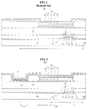
- FIG. 1 is a cross-sectional view showing an organic light emitting diode display device according to a related art.
- the OLED display device 10 includes a substrate 20 and a thin film transistor (TFT) Td and a light emitting diode (LED) De in each pixel region P on the substrate 20.
- TFT thin film transistor
- LED light emitting diode
- a semiconductor layer 22 is formed on the substrate 20, and a gate insulating layer 24 is formed on the semiconductor layer 22.
- the semiconductor layer 22 includes an active region of an intrinsic semiconductor material at a central portion and source and drain regions of an impurity-doped semiconductor material at both sides of the central portion.
- a gate electrode 26 is formed on the gate insulating layer 24 over the semiconductor layer 22, and an interlayer insulating layer 28 is formed on the gate electrode 26.
- the interlayer insulating layer 28 and the gate insulating layer 24 include first and second contact holes exposing the source and drain regions, respectively, of the semiconductor layer 22.
- Source and drain electrodes 30 and 32 spaced apart from each other are formed on the interlayer insulating layer 28 corresponding to the semiconductor layer 22.
- the source and drain electrodes 30 and 32 are connected to the source and drain regions of the semiconductor layer 22 through the first and second contact holes, respectively.
- the semiconductor layer 22, the gate electrode 26, the source electrode 30 and the drain electrode 32 constitute a thin film transistor (TFT) Td.
- a passivation layer 34 is formed on the TFT Td and has a third contact hole exposing the source electrode 30.
- a first electrode 36 is formed on the passivation layer 34 corresponding to a central portion of the pixel region P and is connected to the source electrode 30 through the third contact hole.
- a bank layer 38 is formed on the first electrode 36.
- the bank layer 38 covers an edge portion of the first electrode 36 and has an opening exposing a central portion of the first electrode 36.
- a first emission assisting layer 40 is formed on the first electrode 36 exposed through the opening of the bank layer 38, and an emitting layer 42 is formed on the first emission assisting layer 40 in the opening of the bank layer 38.
- the first emission assisting layer 40 assists injection or transport of carriers (e.g., holes or electrons).
- a second emission assisting layer 44 is formed on the entire surface of the substrate 20 having the emitting layer, and a second electrode 46 is formed on the entire surface of the substrate 20 having the second emission assisting layer 44.
- the second emission assisting layer 44 assists injection or transport of other carriers (e.g., electrons or holes).
- the first emission assisting layer 40 may include a hole injecting layer (HIL) and a hole transporting layer (HTL), and the second emission assisting layer 44 may include an electron injecting layer (EIL) and an electron transporting layer (ETL).
- HIL hole injecting layer
- EIL electron injecting layer
- ETL electron transporting layer
- the first electrode 36, the first emission assisting layer 40, the emitting layer 42, the second emission assisting layer 44 and the second electrode 46 constitute a light emitting diode De.
- the second emission assisting layer 44 is not patterned in each pixel region P. Instead, the second emission assisting layer 44 is formed on the entire surface of the substrate 20 for cost reduction of and yield increase due to process simplification in a product having a large size and a high resolution.
- the second electrode 46 since the second electrode 46 should have transparency in the top emission type OLED display device 10, the second electrode 46 may be formed by depositing a metallic material such as aluminum (Al), magnesium (Mg) and silver (Ag) with a relatively thin thickness.
- a resistance of the second electrode 46 increases due to the relatively thin thickness and non-uniformity in brightness is caused by a voltage drop of a low level voltage VSS.
- second emission assisting layer 44 is formed on the entire surface of the substrate 20, it is required to eliminate the second emission assisting layer 44 on the auxiliary electrode or the auxiliary line for connecting the second electrode 46 to the auxiliary electrode or the auxiliary line.
- a laser patterning and a patterning using a separator have been suggested as a method of eliminating the second emission assisting layer 44 on the auxiliary electrode or the auxiliary line.
- a step of irradiating a laser beam onto the second emission assisting layer 44 on the auxiliary electrode or the auxiliary line is added, therefore a fabrication cost increases and a yield decreases.
- a step of forming the separator is added, thus a fabrication cost increases and a yield decreases.
- the emitting layer 42 can be deteriorated due to a sputtering for forming a transparent conductive layer as an uppermost layer.
- Embodiments relate to an organic light emitting diode display device and a method of fabricating the same that substantially obviate one or more of the problems due to limitations and disadvantages of the related art. Aspects of an invention are defined in the appended independent claims.
- an organic light emitting diode display device comprises: a substrate including a pixel region, the pixel region including a first portion and a second portion; a first electrode in the second portion of the pixel region; a bank layer separating the first portion and the second portion of the pixel region; an emitting layer in the second portion of the pixel region but not in the first portion of the pixel region; an emission assisting layer extending in the first portion of the pixel region, over the bank, and in the second portion of the pixel region, the emission assisting layer in the first portion of the pixel region being more conductive than the emission assisting layer in the second portion of the pixel region; and a second electrode on the emission assisting layer in the first portion of the pixel region, over the bank, and in the second portion of the pixel region.
- the bank layer includes an organic material.
- the organic light emitting diode display device further includes an auxiliary line in the first portion of the pixel region below and in contact with the emission assisting layer.
- the emission assisting layer may have a thickness within a range of 10 ⁇ to 1000 ⁇ , and the emission assisting layer in the second portion of the pixel region between the auxiliary line and the second electrode may have a resistance within a range of 5 ⁇ to 1k ⁇ .
- the organic light emitting diode display device further includes another auxiliary line of a line shape in the first portion of the pixel region under the auxiliary line, wherein said another auxiliary line is connected to the auxiliary line.
- the emission assisting layer in the first portion of the pixel region includes a plurality of conductive particles, the plurality of conductive particles including a same material as one of the auxiliary line and the second electrode.
- the auxiliary line and the first electrode are on a same layer.
- the organic light emitting diode display device further comprises another emission assisting layer in the second portion of the pixel region between the first electrode and the emitting layer.
- the emission assisting layer may include a hole injecting layer and a hole transporting layer, and said another emission assisting layer may include an electron injecting layer and an electron transporting layer.
- One or more embodiments relate to a method of fabricating an organic light emitting diode display device.
- the method comprises: forming an auxiliary line in a first portion of a pixel region on a substrate; forming a first electrode in a second portion of the pixel region on the substrate; forming an emitting layer on the first electrode in the second portion of the pixel region; forming an emission assisting layer on the auxiliary line in the first portion of the pixel region and on the emitting layer in the second portion of the pixel region; forming a second electrode on the emission assisting layer in the first portion of the pixel region and the second portion of the pixel region on the emission assisting layer; and applying a bias voltage to the auxiliary line and the second electrode to induce conductive particles in the emission assisting layer in the first portion of the pixel region.
- the bias voltage is one of a direct current voltage, an alternating current voltage and a pulse voltage.
- the emitting layer and the emission assisting layer are formed through a soluble process.
- the method further includes forming another emission assisting layer in the second portion of the pixel region between the first electrode and the emitting layer.
- the method further includes forming another auxiliary line of a line shape in the first portion of the pixel region under the auxiliary line. Said another auxiliary line may be connected to the auxiliary line.
- the method further includes forming a bank layer between the first portion of the pixel region and the second portion of the pixel region after forming the first electrode in the first portion of the pixel region and the auxiliary line in the second portion of the pixel region.
- the emission assisting layer may be formed on the auxiliary line in the first portion of the pixel region, on the emitting layer in the second portion of the pixel region and on the bank layer between the first portion of the pixel region and the second portion of the pixel region.
- the auxiliary line and the first electrode are formed on a same layer simultaneously.
- FIG. 2 is a cross-sectional view showing a top emission type organic light emitting diode display device according to an embodiment.
- an organic light emitting diode (OLED) display device 110 includes a substrate 120 and a thin film transistor (TFT) Td and a light emitting diode (LED) De in each pixel region P on the substrate 120.
- TFT thin film transistor
- LED light emitting diode
- a semiconductor layer 122 is formed on the substrate 120, which may be referred to as a lower substrate, a TFT substrate or a backplane, and a gate insulating layer 124 is formed on the semiconductor layer 122.
- the semiconductor layer 122 may include an active region of an intrinsic semiconductor material at a central portion and source and drain regions of an impurity-doped semiconductor material at both sides of the central portion.
- a gate electrode 126 is formed on the gate insulating layer 24 over the semiconductor layer 122, and an interlayer insulating layer 128 is formed on the gate electrode 126.
- the interlayer insulating layer 128 and the gate insulating layer 124 include first and second contact holes exposing the source and drain regions, respectively, of the semiconductor layer 122.
- Source and drain electrodes 130 and 132 spaced apart from each other are formed on the interlayer insulating layer 128 corresponding to the semiconductor layer 122.
- the source and drain electrodes 130 and 132 are connected to the source and drain regions of the semiconductor layer 122 through the first and second contact holes, respectively.
- the semiconductor layer 122, the gate electrode 126, the source electrode 130 and the drain electrode 132 constitute a thin film transistor (TFT) Td.
- TFT Td of a coplanar type is formed on the substrate 120 in FIG. 2
- the TFT of a staggered type may be formed on the substrate in another embodiment.
- the driving TFT Td is shown in FIG. 2
- a plurality of TFTs including a switching TFT having the same structure as the driving TFT Td may be further formed in each pixel region P.
- each pixel region P includes a first portion 210 in which an auxiliary electrode is disposed, and a second portion 220 from which light is emitted.
- the switching TFT may be connected to the gate line and the data line, and the driving TFT Td may be connected to the switching TFT and the power line.
- a passivation layer 134 is formed on the TFT Td and has a third contact hole exposing the source electrode 130.
- a first electrode 136 is formed on the passivation layer 134 corresponding to the second portion 220 (e.g., central portion) of the pixel region P, and an auxiliary line 137 is formed on the passivation layer 134 corresponding to a first portion 210 of the pixel region P.
- the first electrode 136 is connected to the source electrode 130 through the third contact hole.
- the auxiliary line 137 may include the same material and be formed in the same layer as the first electrode 136.
- the drain electrode 132 may be exposed through the third contact hole and connected to the first electrode 136 instead of the source electrode 130.
- auxiliary line 137 of a line shape is formed on the passivation layer 134 along the first portion 210 of the pixel region P in FIG. 2
- a first auxiliary line (auxiliary electrode or auxiliary pattern) of an island shape and a second auxiliary line of a line shape connected to each other through a contact hole may be formed over the substrate 120 for further reducing the resistance in another embodiment.
- the first auxiliary line of an island shape having the same material and in the same layer as the first electrode 136 may be formed on the passivation layer 134 at the first portion 210 of the pixel region P.
- the second auxiliary line of a line shape including the same material and in the same layer as the gate electrode 126 may be formed between the gate insulating layer 124 and the interlayer insulating layer 128 along the first portion 210 of the pixel region P.
- the second auxiliary line of a line shape including the same material and the same layer as the source and drain electrodes 130 and 132 may be formed between the interlayer insulating layer 128 and the passivation layer 134 along the first portion 210 of the pixel region P.
- a bank layer 138 is formed on the first electrode 136 and the auxiliary line 137.
- the bank layer 138 covers an edge portion of the first electrode 136 and an edge portion of the auxiliary line 137.
- the bank layer 138 separates the first portion 210 and the second portion 220 of the pixel region P.
- the bank layer 138 has first and second openings exposing a central portion of the first electrode 136 in the second portion 220 of the pixel region P and a central portion of the auxiliary line 137 in the first portion 210 of the pixel region P.
- the bank layer 138 may include an organic insulating material or an inorganic insulating material for maintaining a contact property (e.g., hydrophilic property or hydrophobic property) with a first emission assisting layer 140 and an emitting layer 142 (also referred to as "light emitting layer 142") formed in a subsequent process.
- a contact property e.g., hydrophilic property or hydrophobic property
- emitting layer 142 also referred to as "light emitting layer 142”
- a first emission assisting layer 140 is formed on the first electrode 136 exposed through the first opening of the bank layer 138 in the second portion 220 of the pixel region P, and an emitting layer 142 is formed on the first emission assisting layer 140 in the first opening of the bank layer 138 in the second portion 220 of the pixel region P.
- the first emission assisting layer 140 and the emitting layer 142 may be formed in each pixel region P by patterning an organic material.
- the first emission assisting layer 140 may include a hole injecting layer (HIL) and a hole transporting layer (HTL), and the emitting layer 142 may include individual organic material for each pixel region P to emit a light of different color.
- the first emission assisting layer 140 may be omitted in another embodiment.
- a second emission assisting layer 144 extends over the first portion 210 of the pixel region P, the bank layer 138, and the second portion 220 of the pixel region P.
- a second electrode 146 extends over the first portion 210 of the pixel region P, the bank layer 138, and the second portion 220 of the pixel region P on the second emission assisting layer 144.
- the second emission assisting layer 144 may be formed on the entire surface of the substrate 120 having the emitting layer 142, and the second electrode 146 may be formed on the second emission assisting layer 144 over the entire surface of the substrate 120.
- the second emission assisting layer 144 may include an electron injecting layer (EIL) and an electron transporting layer (ETL) and may have a thickness within a range of about 10 ⁇ to about 1000 ⁇ .
- EIL electron injecting layer
- ETL electron transporting layer
- the first emission assisting layer 140, the emitting layer 142 and the second emission assisting layer 144 may be formed through a soluble process such as an inkjet printing and a nozzle printing.
- the second electrode 146 may be formed through a thermal evaporation.
- the first electrode 136, the first emission assisting layer 140, the emitting layer 142, the second emission assisting layer 144 and the second electrode 146 constitute a light emitting diode De, and the first electrode 136 and the second electrode 146 may be an anode and a cathode, respectively. In other embodiments, the first electrode 136 and the second electrode 146 may be a cathode and an anode, respectively.
- the first electrode 136 may have a single layered structure of a transparent conductive material such as indium tin oxide (ITO) or a double layered structure of a metallic material and a transparent conductive material.
- the second electrode 146 may have a single layered structure of one of aluminum (Al), magnesium (Mg) and silver (Ag) or a double layered structure of at least two of aluminum (Al), magnesium (Mg) and silver (Ag).
- a capping layer including one of an organic material, an inorganic material and a metal oxide material may be formed on the entire surface of the substrate 120 having the second electrode 146.
- the capping layer may have a refractive index greater than about 1.5.
- the capping layer may cover the light emitting diode De to prevent penetration of moisture into the emitting layer 142 of the light emitting diode De.
- the capping layer may minimize reflection of an external light on the second electrode 146 and may increase a transmittance of the second electrode 146.
- an encapsulation substrate may be disposed over the second electrode 146.
- the encapsulation substrate may be attached to the substrate 120 using a seal pattern or a seal layer.
- the second emission assisting layer 144 and the second electrode 146 are sequentially formed on the auxiliary line 137 exposed through the second opening of the bank layer 138. After the second electrode 146 is formed, a bias voltage is applied to the auxiliary line 137 and the second electrode 146 during a fabrication process. As a result, a plurality of conductive particles 147 of the auxiliary line 137 or the second electrode 146 may be induced in the second emission assisting layer 144 due to electromigration.
- the second emission assisting layer 144 between the auxiliary line 137 and the second electrode 146 may include the plurality of conductive particles 147 to have a conductive property or to improve conductivity compared to without the conductive particles 147.
- the second emission assisting layer 144 with the conductive particles 147 in the first portion 210 of the pixel region P is more conductive than the second emission assisting layer 144 in the second portion 220 of the pixel region P without the conductive particles 147.
- the second emission assisting layer 144 between the auxiliary line 137 and the second electrode 146 including the plurality of conductive particles 147 may have a resistance between 5 ⁇ and 1k ⁇ .
- the plurality of conductive particles 147 may include the same material as the auxiliary line 137 or the second electrode 146.
- the auxiliary line 137 and the second electrode 146 are electrically connected to each other through the second emission assisting layer 144. Accordingly, the resistance of the second electrode 146 having a relatively thin thickness can be lowered due to an electrical connection to the auxiliary line 137 through the second emission assisting layer 144, and a voltage drop of a low level voltage VSS applied to the second electrode 146 while the OLED display device 110 is driven can be reduced. As a result, non-uniformity in brightness and deterioration in display quality can be prevented.
- a method of fabricating the OLED display device 110 will be illustrated hereinafter.
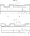
- FIGs. 3A through 3E are cross-sectional views showing a method of fabricating an organic light emitting diode display device according to an embodiment. Illustration for the same parts as those of FIG. 2 may be omitted.
- a semiconductor layer 122 is formed in each pixel region P on a substrate 120, and a gate insulating layer 124 is formed on the entire surface of the substrate 120 having the semiconductor layer 122.
- a gate electrode 126 is formed on the gate insulating layer 124 corresponding to the semiconductor layer 122, and an interlayer insulating layer 128 is formed on the gate electrode 126.
- source and drain electrodes 130 and 132 spaced apart from each other are formed on the interlayer insulating layer 128 corresponding to the semiconductor layer 122.
- the semiconductor layer 122, the gate electrode 126, the source electrode 130 and the drain electrode 132 constitute a thin film transistor (TFT) Td.
- a passivation layer 134 is formed on the TFT Td.
- a first electrode 136 is formed on the passivation layer 134 corresponding to the second portion 220 of the pixel region P, and an auxiliary line 137 is formed on the passivation layer 134 corresponding to the first portion 210 of the pixel region P.
- a bank layer 138 is formed on the first electrode 136 and the auxiliary line 137.
- the bank layer 138 covers an edge portion of the first electrode 136 and an edge portion of the auxiliary line 137.
- the bank layer 138 has a first opening exposing a central portion of the first electrode 136 and a second opening exposing a central portion of the auxiliary line 137.
- a first emission assisting layer 140 is formed on the first electrode 136 exposed through the first opening of the bank layer 138, and an emitting layer 142 is formed in the first opening of the bank layer 138 on the first emission assisting layer 140.
- the first emission assisting layer 140 and the emitting layer 142 may be patterned in each pixel region P through a soluble process such as an inkjet printing and a nozzle printing using an organic material.
- the first emission assisting layer 140 may include a hole injecting layer (HIL) and a hole transporting layer (HTL), and the emitting layer 142 may include individual organic material for each pixel region P to emit a light of different color.
- a second emission assisting layer 144 is formed on the entire surface of the substrate 120 having the emitting layer 142 and the auxiliary line 137, and a second electrode 146 is formed on the entire surface of the substrate 120 having the second emission assisting layer 144.
- the second emission assisting layer 144 may be formed through a soluble process such as an inkjet printing and a nozzle printing using an organic material for reducing a fabrication cost and increasing a yield, and the second electrode 146 may be formed through a thermal evaporation using a metallic material.
- the second emission assisting layer 144 may include an electron injecting layer (EIL) and an electron transporting layer (ETL) and may have a thickness within a range of about 10 ⁇ to about 1000 ⁇ .
- a bias voltage is applied to the auxiliary line 137 and the second electrode 146 during a fabrication process.
- the bias voltage applied to the auxiliary line 137 and the second electrode 146 may be a direct current (DC) voltage, an alternating current (AC) voltage or a pulse voltage having a shape of a rectangular wave.
- DC direct current
- AC alternating current
- pulse voltage having a shape of a rectangular wave.
- voltages within a range of about -20V to about +20V in 0.5V steps may be sequentially applied to the auxiliary line 137 and the second electrode 146.
- the bias voltage may be repeatedly applied to the auxiliary line 137 and the second electrode 146 several times.
- the plurality of conductive particles 147 may include at least one of aluminum (Al), magnesium (Mg) and silver (Ag).
- the second emission assisting layer 144 including the plurality of conductive particles 147 between the auxiliary line 137 and the second electrode 146 attains a conductive property or higher conductivity compared to the second emission assisting layer 144 without the conductive particles 147.
- the auxiliary line 137 and the second electrode 146 can be electrically connected to each other through the second emission assisting layer 144 having a conductive property.
- the second emission assisting layer 144 including the plurality of conductive particles 147 between the auxiliary line 137 and the second electrode 146 may have a resistance between 5 ⁇ and 1k ⁇ .
- FIG. 4 is a graph showing a conductive property of a second emission assisting layer of an organic light emitting diode display device according to an embodiment.
- a second emission assisting layer 144 of FIG. 2 of an electron injecting layer (EIL) is formed of sodium fluoride (NaF) having a thickness of about 40 ⁇
- a second electrode 146 of FIG. 2 is formed of aluminum (Al) having a thickness of about 300 ⁇ .
- a bias voltage is applied to an auxiliary line 137 of FIG. 2 and the second electrode 146.
- a resistance of the second emission assisting layer 144 is measured before and after the bias voltage is applied.
- the resistance of the second emission assisting layer 144 before application of the bias voltage may be within a range of about 6.8k ⁇ to about 8.8k ⁇ , and the resistance of the second emission assisting layer 144 after application of the bias voltage may be within a range of about 3.9 ⁇ to about 4.6 ⁇ .
- the resistance after application of the bias voltage is reduced to about 1/5000 of the resistance before application of the bias voltage.
- the resistance of the second emission assisting layer 144 is reduced from a range of about 10k ⁇ to about 15k ⁇ before application of the bias voltage to a range of about 50 ⁇ to about 73 ⁇ after application of the bias voltage.
- the resistance of the second emission assisting layer 144 is reduced from a range of about 12k ⁇ to about 35k ⁇ before application of the bias voltage to a range of about 78 ⁇ to about 80 ⁇ after application of the bias voltage.
- the resistance of the second emission assisting layer 144 is reduced from a range of about 40k ⁇ to about 71k ⁇ before application of the bias voltage to a range of about 154 ⁇ to about 177 ⁇ after application of the bias voltage.
- the second emission assisting layer 144 Since the resistance of the second emission assisting layer 144 is reduced from a value of several tens of k ⁇ to a value of several hundreds of ⁇ due to application of the bias voltage, the second emission assisting layer including the plurality of conductive particles 147 of FIG. 2 becomes conductive. As a result, the auxiliary line 137 and the second electrode 146 are electrically connected to each other through the second emission assisting layer 144.
- the second emission assisting layer 144 of the light emitting diode De without the conductive particles 147 in the second portion 220 may have a higher resistance (or may be less conductive) than the second emission assisting layer 144 in the first portion 210 with the conductive particles.
- the bias voltage is applied to the auxiliary line 137 and the second electrode 146, and the plurality of conductive particles 147 of the auxiliary line 137 or the second electrode 146 move into the second emission assisting layer 144 between the auxiliary line 137 and the second electrode 146 due to electromigration.
- the second emission assisting layer 144 between the auxiliary line 137 and the second electrode 146 includes the plurality of conductive particles 147 and becomes to have a conductive property. As a result, the auxiliary line 137 and the second electrode 146 are electrically connected to each other through the second emission assisting layer 144.
- the resistance of the second electrode 146 having a relatively thin thickness can be reduced due to the auxiliary line 137.
- non-uniformity in brightness and deterioration in display quality can be prevented by reducing a voltage drop of a low level voltage VSS applied to the second electrode 146.
Landscapes
- Engineering & Computer Science (AREA)
- Physics & Mathematics (AREA)
- Optics & Photonics (AREA)
- Microelectronics & Electronic Packaging (AREA)
- Manufacturing & Machinery (AREA)
- Electroluminescent Light Sources (AREA)
Abstract
Description
- The present disclosure relates to an organic light emitting diode display device, and more particularly, to an organic light emitting diode display device where an electrode of a light emitting diode and an auxiliary line are connected to each other through an emission assisting layer and a method of fabricating the organic light emitting diode display device.
- Among various flat panel displays (FPDs), an organic light emitting diode (OLED) display device has properties such as high luminance and low driving voltage. The OLED display device uses an emissive electroluminescent layer to realize a high contrast ratio and a thin profile, and is excellent at displaying a moving image because of a short response time of several micro seconds (µsec). Also, the OLED display device has no limitation on a viewing angle and is stable even in a low temperature. Since the OLED display device is typically driven by a low voltage (e.g., between 5V and 15V in direct current (DC)), fabrication and design of a driving circuit is easy. Further, a fabrication process for the OLED display device including a deposition and an encapsulation is simple.
- The OLED display device may be classified into a top emission type and a bottom emission type according to a light emission direction. The top emission type OLED display device having an advantage in an aperture ratio has been researched and developed as a product having a large size and a high resolution.
-
FIG. 1 is a cross-sectional view showing an organic light emitting diode display device according to a related art. - In
FIG. 1 , theOLED display device 10 according to the related art includes asubstrate 20 and a thin film transistor (TFT) Td and a light emitting diode (LED) De in each pixel region P on thesubstrate 20. - A
semiconductor layer 22 is formed on thesubstrate 20, and agate insulating layer 24 is formed on thesemiconductor layer 22. Thesemiconductor layer 22 includes an active region of an intrinsic semiconductor material at a central portion and source and drain regions of an impurity-doped semiconductor material at both sides of the central portion. - A
gate electrode 26 is formed on thegate insulating layer 24 over thesemiconductor layer 22, and aninterlayer insulating layer 28 is formed on thegate electrode 26. Theinterlayer insulating layer 28 and thegate insulating layer 24 include first and second contact holes exposing the source and drain regions, respectively, of thesemiconductor layer 22. - Source and
drain electrodes interlayer insulating layer 28 corresponding to thesemiconductor layer 22. The source anddrain electrodes semiconductor layer 22 through the first and second contact holes, respectively. - The
semiconductor layer 22, thegate electrode 26, thesource electrode 30 and thedrain electrode 32 constitute a thin film transistor (TFT) Td. Apassivation layer 34 is formed on the TFT Td and has a third contact hole exposing thesource electrode 30. - A
first electrode 36 is formed on thepassivation layer 34 corresponding to a central portion of the pixel region P and is connected to thesource electrode 30 through the third contact hole. - A
bank layer 38 is formed on thefirst electrode 36. Thebank layer 38 covers an edge portion of thefirst electrode 36 and has an opening exposing a central portion of thefirst electrode 36. - A first
emission assisting layer 40 is formed on thefirst electrode 36 exposed through the opening of thebank layer 38, and anemitting layer 42 is formed on the firstemission assisting layer 40 in the opening of thebank layer 38. The firstemission assisting layer 40 assists injection or transport of carriers (e.g., holes or electrons). - A second
emission assisting layer 44 is formed on the entire surface of thesubstrate 20 having the emitting layer, and asecond electrode 46 is formed on the entire surface of thesubstrate 20 having the secondemission assisting layer 44. The secondemission assisting layer 44 assists injection or transport of other carriers (e.g., electrons or holes). - The first
emission assisting layer 40 may include a hole injecting layer (HIL) and a hole transporting layer (HTL), and the secondemission assisting layer 44 may include an electron injecting layer (EIL) and an electron transporting layer (ETL). Thefirst electrode 36, the firstemission assisting layer 40, theemitting layer 42, the secondemission assisting layer 44 and thesecond electrode 46 constitute a light emitting diode De. - In the
OLED display device 10, the secondemission assisting layer 44 is not patterned in each pixel region P. Instead, the secondemission assisting layer 44 is formed on the entire surface of thesubstrate 20 for cost reduction of and yield increase due to process simplification in a product having a large size and a high resolution. - In addition, since the
second electrode 46 should have transparency in the top emission typeOLED display device 10, thesecond electrode 46 may be formed by depositing a metallic material such as aluminum (Al), magnesium (Mg) and silver (Ag) with a relatively thin thickness. However, a resistance of thesecond electrode 46 increases due to the relatively thin thickness and non-uniformity in brightness is caused by a voltage drop of a low level voltage VSS. - To prevent the non-uniformity in brightness, a structure where the
second electrode 46 is connected to an auxiliary electrode or an auxiliary line of a low resistance material at a border of the pixel region P under theemitting layer 42 has been suggested. - In the product having a large size with a high resolution, however, since second
emission assisting layer 44 is formed on the entire surface of thesubstrate 20, it is required to eliminate the secondemission assisting layer 44 on the auxiliary electrode or the auxiliary line for connecting thesecond electrode 46 to the auxiliary electrode or the auxiliary line. - Accordingly, a laser patterning and a patterning using a separator have been suggested as a method of eliminating the second
emission assisting layer 44 on the auxiliary electrode or the auxiliary line. - However, for laser patterning, a step of irradiating a laser beam onto the second
emission assisting layer 44 on the auxiliary electrode or the auxiliary line is added, therefore a fabrication cost increases and a yield decreases. Similarly, for patterning using the separator, a step of forming the separator is added, thus a fabrication cost increases and a yield decreases. Further, theemitting layer 42 can be deteriorated due to a sputtering for forming a transparent conductive layer as an uppermost layer. - Embodiments relate to an organic light emitting diode display device and a method of fabricating the same that substantially obviate one or more of the problems due to limitations and disadvantages of the related art. Aspects of an invention are defined in the appended independent claims.
- In one or more embodiments, an organic light emitting diode display device comprises: a substrate including a pixel region, the pixel region including a first portion and a second portion; a first electrode in the second portion of the pixel region; a bank layer separating the first portion and the second portion of the pixel region; an emitting layer in the second portion of the pixel region but not in the first portion of the pixel region; an emission assisting layer extending in the first portion of the pixel region, over the bank, and in the second portion of the pixel region, the emission assisting layer in the first portion of the pixel region being more conductive than the emission assisting layer in the second portion of the pixel region; and a second electrode on the emission assisting layer in the first portion of the pixel region, over the bank, and in the second portion of the pixel region.
- In one or more embodiments, the bank layer includes an organic material.
- In one or more embodiments, the organic light emitting diode display device further includes an auxiliary line in the first portion of the pixel region below and in contact with the emission assisting layer. The emission assisting layer may have a thickness within a range of 10Å to 1000Å, and the emission assisting layer in the second portion of the pixel region between the auxiliary line and the second electrode may have a resistance within a range of 5Ω to 1kΩ.
- In one or more embodiments, the organic light emitting diode display device further includes another auxiliary line of a line shape in the first portion of the pixel region under the auxiliary line, wherein said another auxiliary line is connected to the auxiliary line.
- In one or more embodiments, the emission assisting layer in the first portion of the pixel region includes a plurality of conductive particles, the plurality of conductive particles including a same material as one of the auxiliary line and the second electrode.
- In one or more embodiments, the auxiliary line and the first electrode are on a same layer.
- In one or more embodiments, the organic light emitting diode display device further comprises another emission assisting layer in the second portion of the pixel region between the first electrode and the emitting layer. The emission assisting layer may include a hole injecting layer and a hole transporting layer, and said another emission assisting layer may include an electron injecting layer and an electron transporting layer.
- One or more embodiments relate to a method of fabricating an organic light emitting diode display device. The method comprises: forming an auxiliary line in a first portion of a pixel region on a substrate; forming a first electrode in a second portion of the pixel region on the substrate; forming an emitting layer on the first electrode in the second portion of the pixel region; forming an emission assisting layer on the auxiliary line in the first portion of the pixel region and on the emitting layer in the second portion of the pixel region; forming a second electrode on the emission assisting layer in the first portion of the pixel region and the second portion of the pixel region on the emission assisting layer; and applying a bias voltage to the auxiliary line and the second electrode to induce conductive particles in the emission assisting layer in the first portion of the pixel region.
- In one or more embodiments, the bias voltage is one of a direct current voltage, an alternating current voltage and a pulse voltage.
- In one or more embodiments, the emitting layer and the emission assisting layer are formed through a soluble process.
- In one or more embodiments, the method further includes forming another emission assisting layer in the second portion of the pixel region between the first electrode and the emitting layer.
- In one or more embodiments, the method further includes forming another auxiliary line of a line shape in the first portion of the pixel region under the auxiliary line. Said another auxiliary line may be connected to the auxiliary line.
- In one or more embodiments, the method further includes forming a bank layer between the first portion of the pixel region and the second portion of the pixel region after forming the first electrode in the first portion of the pixel region and the auxiliary line in the second portion of the pixel region. The emission assisting layer may be formed on the auxiliary line in the first portion of the pixel region, on the emitting layer in the second portion of the pixel region and on the bank layer between the first portion of the pixel region and the second portion of the pixel region.
- In one or more embodiments, the auxiliary line and the first electrode are formed on a same layer simultaneously.
- Advantages and features of the disclosure will be set forth in part in the description, which follows and in part will become apparent to those having ordinary skill in the art upon examination of the following or may be learned from practice of the disclosure. Other advantages and features of the embodiments herein may be realized and attained by the structure particularly pointed out in the written description and claims hereof as well as the appended drawings.
- It is to be understood that both the foregoing general description and the following detailed description are explanatory, and are intended to provide further explanation of the embodiments as claimed.
- The accompanying drawings, which are included to provide a further understanding of the disclosure, are incorporated in and constitute a part of this specification, illustrate implementations and together with the description serve to explain the principles of embodiments.
-
FIG. 1 is a cross-sectional view showing an organic light emitting diode display device according to a related art. -
FIG. 2 is a cross-sectional view showing a top emission type organic light emitting diode display device according to an embodiment. -
FIGs. 3A through 3E are cross-sectional views showing a method of fabricating an organic light emitting diode display device according to an embodiment. -
FIG. 4 is a graph showing a conductive property of a second emission assisting layer of an organic light emitting diode display device according to an embodiment. - Reference will now be made in detail to embodiments, examples of which are illustrated in the accompanying drawings. In the following description, when a detailed description of well-known functions or configurations related to this document is determined to unnecessarily cloud a description of an embodiment, the detailed description thereof will be omitted. The progression of processing steps and/or operations described is an example; however, the sequence of steps and/or operations is not limited to that set forth herein and may be changed as is known in the art, with the exception of steps and/or operations necessarily occurring in a certain order. Like reference numerals designate like elements throughout. Names of the respective elements used in the following explanations are selected only for convenience of writing the specification and may be thus different from those used in actual products.
-
FIG. 2 is a cross-sectional view showing a top emission type organic light emitting diode display device according to an embodiment. - In
FIG. 2 , an organic light emitting diode (OLED) display device 110 includes asubstrate 120 and a thin film transistor (TFT) Td and a light emitting diode (LED) De in each pixel region P on thesubstrate 120. - A
semiconductor layer 122 is formed on thesubstrate 120, which may be referred to as a lower substrate, a TFT substrate or a backplane, and agate insulating layer 124 is formed on thesemiconductor layer 122. Thesemiconductor layer 122 may include an active region of an intrinsic semiconductor material at a central portion and source and drain regions of an impurity-doped semiconductor material at both sides of the central portion. - A
gate electrode 126 is formed on thegate insulating layer 24 over thesemiconductor layer 122, and an interlayer insulatinglayer 128 is formed on thegate electrode 126. The interlayer insulatinglayer 128 and thegate insulating layer 124 include first and second contact holes exposing the source and drain regions, respectively, of thesemiconductor layer 122. - Source and
drain electrodes interlayer insulating layer 128 corresponding to thesemiconductor layer 122. The source and drainelectrodes semiconductor layer 122 through the first and second contact holes, respectively. - The
semiconductor layer 122, thegate electrode 126, thesource electrode 130 and thedrain electrode 132 constitute a thin film transistor (TFT) Td. Although the TFT Td of a coplanar type is formed on thesubstrate 120 inFIG. 2 , the TFT of a staggered type may be formed on the substrate in another embodiment. Although the driving TFT Td is shown inFIG. 2 , a plurality of TFTs including a switching TFT having the same structure as the driving TFT Td may be further formed in each pixel region P. - Although not shown, a gate line, a data line and a power line may be formed on the
substrate 120. The gate line may cross the data line and the power line to define the pixel region P. In one aspect, each pixel region P includes afirst portion 210 in which an auxiliary electrode is disposed, and asecond portion 220 from which light is emitted. In addition, the switching TFT may be connected to the gate line and the data line, and the driving TFT Td may be connected to the switching TFT and the power line. - A
passivation layer 134 is formed on the TFT Td and has a third contact hole exposing thesource electrode 130. - A
first electrode 136 is formed on thepassivation layer 134 corresponding to the second portion 220 (e.g., central portion) of the pixel region P, and anauxiliary line 137 is formed on thepassivation layer 134 corresponding to afirst portion 210 of the pixel region P. Thefirst electrode 136 is connected to thesource electrode 130 through the third contact hole. Theauxiliary line 137 may include the same material and be formed in the same layer as thefirst electrode 136. - In one or more embodiments, the
drain electrode 132 may be exposed through the third contact hole and connected to thefirst electrode 136 instead of thesource electrode 130. - Although the
auxiliary line 137 of a line shape is formed on thepassivation layer 134 along thefirst portion 210 of the pixel region P inFIG. 2 , a first auxiliary line (auxiliary electrode or auxiliary pattern) of an island shape and a second auxiliary line of a line shape connected to each other through a contact hole may be formed over thesubstrate 120 for further reducing the resistance in another embodiment. For example, the first auxiliary line of an island shape having the same material and in the same layer as thefirst electrode 136 may be formed on thepassivation layer 134 at thefirst portion 210 of the pixel region P. In addition, the second auxiliary line of a line shape including the same material and in the same layer as thegate electrode 126 may be formed between thegate insulating layer 124 and the interlayer insulatinglayer 128 along thefirst portion 210 of the pixel region P. Alternatively, the second auxiliary line of a line shape including the same material and the same layer as the source and drainelectrodes layer 128 and thepassivation layer 134 along thefirst portion 210 of the pixel region P. - A
bank layer 138 is formed on thefirst electrode 136 and theauxiliary line 137. Thebank layer 138 covers an edge portion of thefirst electrode 136 and an edge portion of theauxiliary line 137. In one or more embodiments, thebank layer 138 separates thefirst portion 210 and thesecond portion 220 of the pixel region P. In addition, thebank layer 138 has first and second openings exposing a central portion of thefirst electrode 136 in thesecond portion 220 of the pixel region P and a central portion of theauxiliary line 137 in thefirst portion 210 of the pixel region P. - The
bank layer 138 may include an organic insulating material or an inorganic insulating material for maintaining a contact property (e.g., hydrophilic property or hydrophobic property) with a firstemission assisting layer 140 and an emitting layer 142 (also referred to as "light emittinglayer 142") formed in a subsequent process. - A first
emission assisting layer 140 is formed on thefirst electrode 136 exposed through the first opening of thebank layer 138 in thesecond portion 220 of the pixel region P, and an emittinglayer 142 is formed on the firstemission assisting layer 140 in the first opening of thebank layer 138 in thesecond portion 220 of the pixel region P. The firstemission assisting layer 140 and the emittinglayer 142 may be formed in each pixel region P by patterning an organic material. - The first
emission assisting layer 140 may include a hole injecting layer (HIL) and a hole transporting layer (HTL), and the emittinglayer 142 may include individual organic material for each pixel region P to emit a light of different color. The firstemission assisting layer 140 may be omitted in another embodiment. - In one or more embodiments, a second
emission assisting layer 144 extends over thefirst portion 210 of the pixel region P, thebank layer 138, and thesecond portion 220 of the pixel region P. Similarly, asecond electrode 146 extends over thefirst portion 210 of the pixel region P, thebank layer 138, and thesecond portion 220 of the pixel region P on the secondemission assisting layer 144. In one embodiment, the secondemission assisting layer 144 may be formed on the entire surface of thesubstrate 120 having the emittinglayer 142, and thesecond electrode 146 may be formed on the secondemission assisting layer 144 over the entire surface of thesubstrate 120. - The second
emission assisting layer 144 may include an electron injecting layer (EIL) and an electron transporting layer (ETL) and may have a thickness within a range of about 10Å to about 1000Å. - The first
emission assisting layer 140, the emittinglayer 142 and the secondemission assisting layer 144 may be formed through a soluble process such as an inkjet printing and a nozzle printing. Thesecond electrode 146 may be formed through a thermal evaporation. - The
first electrode 136, the firstemission assisting layer 140, the emittinglayer 142, the secondemission assisting layer 144 and thesecond electrode 146 constitute a light emitting diode De, and thefirst electrode 136 and thesecond electrode 146 may be an anode and a cathode, respectively. In other embodiments, thefirst electrode 136 and thesecond electrode 146 may be a cathode and an anode, respectively. - For example, the
first electrode 136 may have a single layered structure of a transparent conductive material such as indium tin oxide (ITO) or a double layered structure of a metallic material and a transparent conductive material. Thesecond electrode 146 may have a single layered structure of one of aluminum (Al), magnesium (Mg) and silver (Ag) or a double layered structure of at least two of aluminum (Al), magnesium (Mg) and silver (Ag). - Although not shown in
FIG. 2 , a capping layer including one of an organic material, an inorganic material and a metal oxide material may be formed on the entire surface of thesubstrate 120 having thesecond electrode 146. The capping layer may have a refractive index greater than about 1.5. The capping layer may cover the light emitting diode De to prevent penetration of moisture into the emittinglayer 142 of the light emitting diode De. In addition, the capping layer may minimize reflection of an external light on thesecond electrode 146 and may increase a transmittance of thesecond electrode 146. - Further, an encapsulation substrate may be disposed over the
second electrode 146. The encapsulation substrate may be attached to thesubstrate 120 using a seal pattern or a seal layer. - In the OLED display device 110, the second
emission assisting layer 144 and thesecond electrode 146 are sequentially formed on theauxiliary line 137 exposed through the second opening of thebank layer 138. After thesecond electrode 146 is formed, a bias voltage is applied to theauxiliary line 137 and thesecond electrode 146 during a fabrication process. As a result, a plurality ofconductive particles 147 of theauxiliary line 137 or thesecond electrode 146 may be induced in the secondemission assisting layer 144 due to electromigration. - Accordingly, the second
emission assisting layer 144 between theauxiliary line 137 and thesecond electrode 146 may include the plurality ofconductive particles 147 to have a conductive property or to improve conductivity compared to without theconductive particles 147. - The second
emission assisting layer 144 with theconductive particles 147 in thefirst portion 210 of the pixel region P is more conductive than the secondemission assisting layer 144 in thesecond portion 220 of the pixel region P without theconductive particles 147. For example, the secondemission assisting layer 144 between theauxiliary line 137 and thesecond electrode 146 including the plurality ofconductive particles 147 may have a resistance between 5Ω and 1kΩ. The plurality ofconductive particles 147 may include the same material as theauxiliary line 137 or thesecond electrode 146. - Since the second
emission assisting layer 144 between theauxiliary line 137 and thesecond electrode 146 in thefirst portion 210 of the pixel region P has a conductive property or has improved conductivity due to theconductive particles 147 compared to the secondemission assisting layer 144 in thesecond portion 220 of the pixel region P, theauxiliary line 137 and thesecond electrode 146 are electrically connected to each other through the secondemission assisting layer 144. Accordingly, the resistance of thesecond electrode 146 having a relatively thin thickness can be lowered due to an electrical connection to theauxiliary line 137 through the secondemission assisting layer 144, and a voltage drop of a low level voltage VSS applied to thesecond electrode 146 while the OLED display device 110 is driven can be reduced. As a result, non-uniformity in brightness and deterioration in display quality can be prevented. - A method of fabricating the OLED display device 110 will be illustrated hereinafter.
-
FIGs. 3A through 3E are cross-sectional views showing a method of fabricating an organic light emitting diode display device according to an embodiment. Illustration for the same parts as those ofFIG. 2 may be omitted. - In
FIG. 3A , asemiconductor layer 122 is formed in each pixel region P on asubstrate 120, and agate insulating layer 124 is formed on the entire surface of thesubstrate 120 having thesemiconductor layer 122. - Next, a
gate electrode 126 is formed on thegate insulating layer 124 corresponding to thesemiconductor layer 122, and an interlayer insulatinglayer 128 is formed on thegate electrode 126. - Next, source and drain
electrodes interlayer insulating layer 128 corresponding to thesemiconductor layer 122. Thesemiconductor layer 122, thegate electrode 126, thesource electrode 130 and thedrain electrode 132 constitute a thin film transistor (TFT) Td. - Next, a
passivation layer 134 is formed on the TFT Td. - Next, a
first electrode 136 is formed on thepassivation layer 134 corresponding to thesecond portion 220 of the pixel region P, and anauxiliary line 137 is formed on thepassivation layer 134 corresponding to thefirst portion 210 of the pixel region P. - Next, a
bank layer 138 is formed on thefirst electrode 136 and theauxiliary line 137. Thebank layer 138 covers an edge portion of thefirst electrode 136 and an edge portion of theauxiliary line 137. In addition, thebank layer 138 has a first opening exposing a central portion of thefirst electrode 136 and a second opening exposing a central portion of theauxiliary line 137. - In
FIG. 3B , a firstemission assisting layer 140 is formed on thefirst electrode 136 exposed through the first opening of thebank layer 138, and an emittinglayer 142 is formed in the first opening of thebank layer 138 on the firstemission assisting layer 140. The firstemission assisting layer 140 and the emittinglayer 142 may be patterned in each pixel region P through a soluble process such as an inkjet printing and a nozzle printing using an organic material. In addition, the firstemission assisting layer 140 may include a hole injecting layer (HIL) and a hole transporting layer (HTL), and the emittinglayer 142 may include individual organic material for each pixel region P to emit a light of different color. - In
FIG. 3C , a secondemission assisting layer 144 is formed on the entire surface of thesubstrate 120 having the emittinglayer 142 and theauxiliary line 137, and asecond electrode 146 is formed on the entire surface of thesubstrate 120 having the secondemission assisting layer 144. The secondemission assisting layer 144 may be formed through a soluble process such as an inkjet printing and a nozzle printing using an organic material for reducing a fabrication cost and increasing a yield, and thesecond electrode 146 may be formed through a thermal evaporation using a metallic material. In addition, the secondemission assisting layer 144 may include an electron injecting layer (EIL) and an electron transporting layer (ETL) and may have a thickness within a range of about 10Å to about 1000Å. - In
FIG. 3D , a bias voltage is applied to theauxiliary line 137 and thesecond electrode 146 during a fabrication process. The bias voltage applied to theauxiliary line 137 and thesecond electrode 146 may be a direct current (DC) voltage, an alternating current (AC) voltage or a pulse voltage having a shape of a rectangular wave. For example, voltages within a range of about -20V to about +20V in 0.5V steps may be sequentially applied to theauxiliary line 137 and thesecond electrode 146. In addition, the bias voltage may be repeatedly applied to theauxiliary line 137 and thesecond electrode 146 several times. - In
FIG. 3E , a part of a material constituting theauxiliary line 137 or thesecond electrode 146 moves into the secondemission assisting layer 144 due to an electromigration by the bias voltage applied to theauxiliary line 137 and thesecond electrode 146 to become a plurality ofconductive particles 147. For example, the plurality ofconductive particles 147 may include at least one of aluminum (Al), magnesium (Mg) and silver (Ag). - As a result, the second
emission assisting layer 144 including the plurality ofconductive particles 147 between theauxiliary line 137 and thesecond electrode 146 attains a conductive property or higher conductivity compared to the secondemission assisting layer 144 without theconductive particles 147. Thus, theauxiliary line 137 and thesecond electrode 146 can be electrically connected to each other through the secondemission assisting layer 144 having a conductive property. For example, the secondemission assisting layer 144 including the plurality ofconductive particles 147 between theauxiliary line 137 and thesecond electrode 146 may have a resistance between 5Ω and 1kΩ. -
FIG. 4 is a graph showing a conductive property of a second emission assisting layer of an organic light emitting diode display device according to an embodiment. - In
FIG. 4 , a secondemission assisting layer 144 ofFIG. 2 of an electron injecting layer (EIL) is formed of sodium fluoride (NaF) having a thickness of about 40Å, and asecond electrode 146 ofFIG. 2 is formed of aluminum (Al) having a thickness of about 300Å. Next, a bias voltage is applied to anauxiliary line 137 ofFIG. 2 and thesecond electrode 146. A resistance of the secondemission assisting layer 144 is measured before and after the bias voltage is applied. For example, the resistance of the secondemission assisting layer 144 before application of the bias voltage may be within a range of about 6.8kΩ to about 8.8kΩ, and the resistance of the secondemission assisting layer 144 after application of the bias voltage may be within a range of about 3.9Ω to about 4.6Ω. As a result, the resistance after application of the bias voltage is reduced to about 1/5000 of the resistance before application of the bias voltage. - Although not shown, when the second
emission assisting layer 144 is formed of sodium fluoride (NaF) having a thickness of about 100Å and thesecond electrode 146 is formed of aluminum (Al) having a thickness of about 300Å, the resistance of the secondemission assisting layer 144 is reduced from a range of about 10kΩ to about 15kΩ before application of the bias voltage to a range of about 50Ω to about 73Ω after application of the bias voltage. - In addition, when the second
emission assisting layer 144 is formed of sodium fluoride (NaF) having a thickness of about 200Å and thesecond electrode 146 is formed of aluminum (Al) having a thickness of about 1000Å, the resistance of the secondemission assisting layer 144 is reduced from a range of about 12kΩ to about 35kΩ before application of the bias voltage to a range of about 78Ω to about 80Ω after application of the bias voltage. - Further, when the second
emission assisting layer 144 is formed of sodium fluoride (NaF) having a thickness of about 300Å and thesecond electrode 146 is formed of aluminum (Al) having a thickness of about 1000Å, the resistance of the secondemission assisting layer 144 is reduced from a range of about 40kΩ to about 71kΩ before application of the bias voltage to a range of about 154Ω to about 177Ω after application of the bias voltage. - Since the resistance of the second
emission assisting layer 144 is reduced from a value of several tens of kΩ to a value of several hundreds of Ω due to application of the bias voltage, the second emission assisting layer including the plurality ofconductive particles 147 ofFIG. 2 becomes conductive. As a result, theauxiliary line 137 and thesecond electrode 146 are electrically connected to each other through the secondemission assisting layer 144. However, the secondemission assisting layer 144 of the light emitting diode De without theconductive particles 147 in thesecond portion 220 may have a higher resistance (or may be less conductive) than the secondemission assisting layer 144 in thefirst portion 210 with the conductive particles. - Consequently, in the OLED display device 110 according to an embodiment, after the
second electrode 146 is formed, the bias voltage is applied to theauxiliary line 137 and thesecond electrode 146, and the plurality ofconductive particles 147 of theauxiliary line 137 or thesecond electrode 146 move into the secondemission assisting layer 144 between theauxiliary line 137 and thesecond electrode 146 due to electromigration. - The second
emission assisting layer 144 between theauxiliary line 137 and thesecond electrode 146 includes the plurality ofconductive particles 147 and becomes to have a conductive property. As a result, theauxiliary line 137 and thesecond electrode 146 are electrically connected to each other through the secondemission assisting layer 144. - Accordingly, the resistance of the
second electrode 146 having a relatively thin thickness can be reduced due to theauxiliary line 137. In addition, non-uniformity in brightness and deterioration in display quality can be prevented by reducing a voltage drop of a low level voltage VSS applied to thesecond electrode 146. - A number of examples have been described above. Nevertheless, it will be understood that various modifications may be made. For example, suitable results may be achieved if the described techniques are performed in a different order and/or if components in a described system, architecture, device, or circuit are combined in a different manner and/or replaced or supplemented by other components or their equivalents. Accordingly, other implementations are within the scope of the following claims.
Claims (15)
- An organic light emitting diode display device comprising:a substrate (120) defining a pixel region, the pixel region including a first portion (210) and a second portion (220);a first electrode (136) in the second portion of the pixel region;a bank (138) separating the first portion (210) and the second portion (220) of the pixel region;an emitting layer (142) in the second portion (220) of the pixel region but not in the first portion (210) of the pixel region;an first emission assisting layer (144) extending in the first portion (210) of the pixel region, over the bank (138), and in the second portion (220) of the pixel region, wherein the portion of the first emission assisting layer over the first portion of the pixel region is arranged to be more conductive than the portion of the first emission assisting layer in the second portion of the pixel region; anda second electrode (146) over the: first emission assisting layer (144) in the first portion of the pixel region, over the bank (138), and in the second portion (220) of the pixel region.
- The display device of claim 1, wherein the bank (138) comprises an organic material.
- The display device of claim 1 or 2, further comprising a first auxiliary line (137) in the first portion (210) of the pixel region, wherein the first auxiliary line is between the first emission assisting layer (144) and substrate (120) and in contact with the first emission assisting layer (144).
- The display device of claim 3, wherein the first emission assisting layer (144) has a thickness within the range of 10Å to 1000Å, and the portion of the first emission assisting layer between the first auxiliary line (137) and the second electrode (146) in the second portion (220) of the pixel region has a resistance within a range of 5Ω to 1kΩ.
- The display device of claim 3 or 4, further comprising a second auxiliary line of a line shape in the first portion of the pixel region under the first auxiliary line, wherein said second auxiliary line is connected to the first auxiliary line (137).
- The display device of any of claims 3, 4 or 5, wherein the portion of the first emission assisting layer (144) in the first portion (210) of the pixel region includes a plurality of conductive particles, the plurality of conductive particles including the same material as one of the first auxiliary line (137) and the second electrode (146).
- The display device of any of claims 3-6, wherein the first auxiliary line (137) and the first electrode (136) are formed of the same material.
- The display device of any preceding claim, further comprising a second emission assisting layer in the second portion (220) of the pixel region and between the first electrode (136) and the emitting layer (142).
- The display device of claim 8, wherein the first emission assisting layer (144) comprises a hole injecting layer and a hole transporting layer, and said second emission assisting layer comprises an electron injecting layer and an electron transporting layer.
- A method of fabricating an organic light emitting diode display device comprising:forming a first auxiliary line (137) in a first portion (210) of a pixel region defined by a substrate (120);forming a first electrode (136) in a second portion (220) of the pixel region;forming an emitting layer (142) over on the first electrode (136) in the second portion (220) of the pixel region;forming a first emission assisting layer (144) over on the first auxiliary line (137) in the first portion (210) of the pixel region and over the emitting layer (142) in the second portion (220) of the pixel region;forming a second electrode (146) over: the first emission assisting layer (144) in the first portion (210) of the pixel region and the second portion (220) of the pixel region; andapplying a bias voltage between the first auxiliary line (137) and the second electrode to induce conductive particles into the first emission assisting layer (144) in the first portion (210) of the pixel region.
- The method of claim 10, wherein the bias voltage is one of a direct current voltage, an alternating current voltage and a pulse voltage.
- The method of claim 10 or 11, wherein the emitting layer (142) and the first emission assisting layer (144) are formed through a soluble process.
- The method of any of claims 10, 11 or 12, further comprising forming a second emission assisting layer in the second portion (220) of the pixel region between the first electrode (136) and the emitting layer (142),
and/or
further comprising forming a second auxiliary line of a line shape in the first portion (210) of the pixel region under the first auxiliary line (137), wherein said second auxiliary line is connected to the first auxiliary line (137). - The method of any of claims 10-13, further comprising:forming a bank (138) between the first portion (210) of the pixel region and the second portion (220) of the pixel region after forming the first electrode (136) in the first portion of the pixel region and the first auxiliary line (137) in the second portion (220) of the pixel region,wherein the first emission assisting layer (144) is formed over the first auxiliary line (137) in the first portion (210) of the pixel region, over the emitting layer (142) in the second portion (220) of the pixel region and over the bank (138).
- The method of any of claims 10-14, wherein the first auxiliary line (137) and the first electrode (136) are formed in the same layer simultaneously.
Applications Claiming Priority (1)
| Application Number | Priority Date | Filing Date | Title |
|---|---|---|---|
| KR1020150093273A KR102458597B1 (en) | 2015-06-30 | 2015-06-30 | Organic Light Emitting Diode Display Device And Method Of Fabricating The Same |
Publications (2)
| Publication Number | Publication Date |
|---|---|
| EP3113229A1 true EP3113229A1 (en) | 2017-01-04 |
| EP3113229B1 EP3113229B1 (en) | 2020-12-02 |
Family
ID=56321796
Family Applications (1)
| Application Number | Title | Priority Date | Filing Date |
|---|---|---|---|
| EP16177102.7A Active EP3113229B1 (en) | 2015-06-30 | 2016-06-30 | Organic light emitting diode display device and method of fabricating the same |
Country Status (4)
| Country | Link |
|---|---|
| US (2) | US9825115B2 (en) |
| EP (1) | EP3113229B1 (en) |
| KR (1) | KR102458597B1 (en) |
| CN (2) | CN106328676B (en) |
Cited By (1)
| Publication number | Priority date | Publication date | Assignee | Title |
|---|---|---|---|---|
| EP3499576A1 (en) * | 2017-12-15 | 2019-06-19 | Samsung Display Co., Ltd. | Display device and manufacturing method thereof |
Families Citing this family (32)
| Publication number | Priority date | Publication date | Assignee | Title |
|---|---|---|---|---|
| CA3002752A1 (en) | 2015-10-26 | 2017-05-04 | Oti Lumionics Inc. | Method for patterning a coating on a surface and device including a patterned coating |
| US11224274B2 (en) * | 2015-12-28 | 2022-01-18 | Kiss Nail Products, Inc. | Hairstyling apparatuses and related methods |
| US11457712B2 (en) * | 2015-12-28 | 2022-10-04 | Kiss Nail Products, Inc. | Hairstyling apparatuses and related methods |
| US12232595B2 (en) | 2015-12-28 | 2025-02-25 | Kiss Nail Products, Inc. | Hairstyling apparatuses and related methods |
| KR102802931B1 (en) | 2016-12-02 | 2025-05-08 | 오티아이 루미오닉스 인크. | Device including a conductive coating disposed over emissive regions and method therefor |
| US11916096B2 (en) * | 2017-02-09 | 2024-02-27 | Vuereal Inc. | Circuit and system integration onto a micro-device substrate |
| KR102563713B1 (en) | 2017-04-26 | 2023-08-07 | 오티아이 루미오닉스 인크. | Methods of patterning the coating of a surface and apparatus comprising the patterned coating |
| CN110832660B (en) | 2017-05-17 | 2023-07-28 | Oti照明公司 | Method of selectively depositing a conductive coating on a patterned coating and an apparatus comprising the conductive coating |
| JP2019045767A (en) * | 2017-09-05 | 2019-03-22 | 株式会社ジャパンディスプレイ | Display device |
| KR102457997B1 (en) * | 2017-12-29 | 2022-10-21 | 엘지디스플레이 주식회사 | Electroluminescent Display Device |
| US11751415B2 (en) | 2018-02-02 | 2023-09-05 | Oti Lumionics Inc. | Materials for forming a nucleation-inhibiting coating and devices incorporating same |
| CN108511489B (en) * | 2018-03-07 | 2020-11-03 | 深圳市华星光电半导体显示技术有限公司 | OLED display panel and preparation method thereof |
| US20190280059A1 (en) * | 2018-03-07 | 2019-09-12 | Shenzhen China Star Optoelectronics Semiconductor Display Technology Co., Ltd. | Oled display panel and manufacturing method thereof |
| US11489136B2 (en) | 2018-05-07 | 2022-11-01 | Oti Lumionics Inc. | Method for providing an auxiliary electrode and device including an auxiliary electrode |
| JP7307725B2 (en) * | 2018-06-12 | 2023-07-12 | ソニーセミコンダクタソリューションズ株式会社 | Solid-state image sensor, imaging device, and control method for solid-state image sensor |
| JP2022508040A (en) | 2018-11-23 | 2022-01-19 | オーティーアイ ルミオニクス インコーポレーテッド | Optoelectronic device containing light transmission region |
| KR20250160226A (en) | 2019-03-07 | 2025-11-11 | 오티아이 루미오닉스 인크. | Materials for forming a nucleation-inhibiting coating and devices incorporating same |
| JP7555600B2 (en) | 2019-04-18 | 2024-09-25 | オーティーアイ ルミオニクス インコーポレーテッド | Materials for forming nucleation-inhibiting coatings and devices incorporating same - Patents.com |
| CN110048022B (en) * | 2019-04-22 | 2020-08-04 | 深圳市华星光电半导体显示技术有限公司 | O L ED device and preparation method thereof |
| JP7576337B2 (en) | 2019-05-08 | 2024-11-01 | オーティーアイ ルミオニクス インコーポレーテッド | Materials for forming nucleation-inhibiting coatings and devices incorporating same - Patents.com |
| CN110212114B (en) | 2019-06-03 | 2021-01-29 | 京东方科技集团股份有限公司 | Display substrate, display panel and preparation method thereof, and display device |
| KR20240134240A (en) | 2019-06-26 | 2024-09-06 | 오티아이 루미오닉스 인크. | Optoelectronic device including light transmissive regions with light diffraction characteristics |
| US11832473B2 (en) | 2019-06-26 | 2023-11-28 | Oti Lumionics Inc. | Optoelectronic device including light transmissive regions, with light diffraction characteristics |
| KR102818817B1 (en) | 2019-08-09 | 2025-06-11 | 오티아이 루미오닉스 인크. | Optoelectronic device including auxiliary electrode and partition |
| CN110635066A (en) * | 2019-09-26 | 2019-12-31 | 京东方科技集团股份有限公司 | A transparent display substrate, its manufacturing method, and a transparent display device |
| CN115552643B (en) | 2019-12-24 | 2025-08-19 | Oti照明公司 | Light emitting device including cover layer and method of manufacturing the same |
| CN111525042A (en) * | 2020-04-26 | 2020-08-11 | 深圳市华星光电半导体显示技术有限公司 | Organic light emitting diode display panel and manufacturing method thereof |
| CN112103399A (en) * | 2020-09-23 | 2020-12-18 | 合肥鑫晟光电科技有限公司 | Display panel, manufacturing method thereof and display device |
| US11985841B2 (en) | 2020-12-07 | 2024-05-14 | Oti Lumionics Inc. | Patterning a conductive deposited layer using a nucleation inhibiting coating and an underlying metallic coating |
| JP7647104B2 (en) * | 2021-01-06 | 2025-03-18 | 富士電機株式会社 | Semiconductor Device |
| CN114784064A (en) * | 2022-04-11 | 2022-07-22 | 深圳市华星光电半导体显示技术有限公司 | OLED display panel and OLED display device |
| KR102808858B1 (en) | 2024-02-05 | 2025-05-21 | 박명희 | Curling iron with a double cover for holding hair efficiently |
Citations (3)
| Publication number | Priority date | Publication date | Assignee | Title |
|---|---|---|---|---|
| US20100289417A1 (en) * | 2009-05-18 | 2010-11-18 | Seiko Epson Corporation | Light-emitting device, method for manufacturing the same, display device, and electronic apparatus |
| US20100302221A1 (en) * | 2008-12-18 | 2010-12-02 | Panasonic Corporation | Organic electroluminescence display device and manufacturing method thereof |
| US20140131692A1 (en) * | 2012-05-31 | 2014-05-15 | Panasonic Corporation | Organic el element, organic el panel, organic el light-emitting apparatus and organic el display apparatus |
Family Cites Families (18)
| Publication number | Priority date | Publication date | Assignee | Title |
|---|---|---|---|---|
| KR100587486B1 (en) * | 2004-09-08 | 2006-06-09 | 한국전자통신연구원 | Image and life measurement device of display panel |
| TWI291309B (en) * | 2004-10-28 | 2007-12-11 | Pioneer Corp | Organic electroluminescent display panel and method for manufacturing same |
| US7994711B2 (en) * | 2005-08-08 | 2011-08-09 | Semiconductor Energy Laboratory Co., Ltd. | Light emitting device and manufacturing method thereof |
| KR100805154B1 (en) * | 2006-09-15 | 2008-02-21 | 삼성에스디아이 주식회사 | OLED display and manufacturing method thereof |
| WO2009110186A1 (en) * | 2008-03-04 | 2009-09-11 | パナソニック株式会社 | Light-emitting element and display device |
| KR101574211B1 (en) * | 2008-09-05 | 2015-12-07 | 삼성디스플레이 주식회사 | Organic light emitting diode display |
| JP5157825B2 (en) * | 2008-10-29 | 2013-03-06 | ソニー株式会社 | Manufacturing method of organic EL display |
| KR101056229B1 (en) * | 2009-10-12 | 2011-08-11 | 삼성모바일디스플레이주식회사 | An organic light emitting display device comprising a thin film transistor, a method of manufacturing the same, and a thin film transistor |
| FR2953068B1 (en) * | 2009-11-24 | 2012-01-20 | Commissariat Energie Atomique | ELECTRONIC DISPLAY DEVICE WITH ELECTROLUMINESCENT SCREEN, AND METHOD FOR MANUFACTURING THE SAME |
| GB201118997D0 (en) * | 2011-11-03 | 2011-12-14 | Cambridge Display Tech Ltd | Electronic device and method |
| KR20140064328A (en) * | 2012-11-20 | 2014-05-28 | 엘지디스플레이 주식회사 | Organic electro-luminescent device and method of fabricating the same |
| KR102079251B1 (en) * | 2013-05-21 | 2020-04-08 | 삼성디스플레이 주식회사 | Organic light emitting display apparatus and method for manufacturing the same |
| KR20150009126A (en) * | 2013-07-15 | 2015-01-26 | 삼성디스플레이 주식회사 | Organic light emitting diode display and method for manufacturing the same |
| CN103353701B (en) * | 2013-07-22 | 2015-08-19 | 京东方科技集团股份有限公司 | A kind of display panel, display device, display panel method for making and display packing |
| JP2015125808A (en) * | 2013-12-25 | 2015-07-06 | 三星ディスプレイ株式會社Samsung Display Co.,Ltd. | Display device |
| JP2015207484A (en) * | 2014-04-22 | 2015-11-19 | 三星ディスプレイ株式會社Samsung Display Co.,Ltd. | Display device, and manufacturing method of display device |
| KR102357269B1 (en) * | 2014-12-12 | 2022-02-03 | 삼성디스플레이 주식회사 | Organic light emitting display device and method of manufacturing the same |
| KR102390441B1 (en) * | 2015-10-15 | 2022-04-26 | 삼성디스플레이 주식회사 | Organic light emitting display device |
-
2015
- 2015-06-30 KR KR1020150093273A patent/KR102458597B1/en active Active
-
2016
- 2016-06-15 US US15/183,166 patent/US9825115B2/en active Active
- 2016-06-24 CN CN201610474927.8A patent/CN106328676B/en active Active
- 2016-06-24 CN CN201910505703.2A patent/CN110246878B/en active Active
- 2016-06-30 EP EP16177102.7A patent/EP3113229B1/en active Active
-
2017
- 2017-10-19 US US15/788,665 patent/US10229965B2/en active Active
Patent Citations (3)
| Publication number | Priority date | Publication date | Assignee | Title |
|---|---|---|---|---|
| US20100302221A1 (en) * | 2008-12-18 | 2010-12-02 | Panasonic Corporation | Organic electroluminescence display device and manufacturing method thereof |
| US20100289417A1 (en) * | 2009-05-18 | 2010-11-18 | Seiko Epson Corporation | Light-emitting device, method for manufacturing the same, display device, and electronic apparatus |
| US20140131692A1 (en) * | 2012-05-31 | 2014-05-15 | Panasonic Corporation | Organic el element, organic el panel, organic el light-emitting apparatus and organic el display apparatus |
Cited By (3)
| Publication number | Priority date | Publication date | Assignee | Title |
|---|---|---|---|---|
| EP3499576A1 (en) * | 2017-12-15 | 2019-06-19 | Samsung Display Co., Ltd. | Display device and manufacturing method thereof |
| US10903283B2 (en) | 2017-12-15 | 2021-01-26 | Samsung Display Co., Ltd. | Display device and manufacturing method thereof |
| US12075685B2 (en) | 2017-12-15 | 2024-08-27 | Samsung Display Co., Ltd. | Display device and manufacturing method thereof |
Also Published As
| Publication number | Publication date |
|---|---|
| CN110246878A (en) | 2019-09-17 |
| KR20170003804A (en) | 2017-01-10 |
| US9825115B2 (en) | 2017-11-21 |
| US20170005158A1 (en) | 2017-01-05 |
| CN106328676A (en) | 2017-01-11 |
| KR102458597B1 (en) | 2022-10-25 |
| US10229965B2 (en) | 2019-03-12 |
| CN106328676B (en) | 2019-07-05 |
| US20180040685A1 (en) | 2018-02-08 |
| CN110246878B (en) | 2023-05-19 |
| EP3113229B1 (en) | 2020-12-02 |
Similar Documents
| Publication | Publication Date | Title |
|---|---|---|
| US10229965B2 (en) | Method fabricating organic light emitting diode display device | |
| CN104733500B (en) | Organic light-emitting display device and its restorative procedure | |
| KR102020805B1 (en) | Transparent organic light emitting display device and method for manufacturing the same | |
| JP6211873B2 (en) | Organic EL display device and method of manufacturing organic EL display device | |
| US8963137B2 (en) | Organic light-emitting display device and method of fabricating the same | |
| US8901563B2 (en) | Organic light-emitting display device and method of manufacturing the same | |
| KR101966847B1 (en) | Organic light emitting diode display and method for manufacturing the same | |
| US20130056784A1 (en) | Organic Light-Emitting Display Device and Method of Fabricating the Same | |
| US9547036B2 (en) | Organic light emitting diode display, and fabricating and inspecting methods thereof | |
| US9070598B2 (en) | Thin film transistor array panel and organic light emitting diode display including the same, method for cutting wire in thin film transistor array panel | |
| KR20110138787A (en) | Organic electroluminescent device and manufacturing method thereof | |
| JP6223070B2 (en) | Organic EL display device and method of manufacturing organic EL display device | |
| US20180151637A1 (en) | Organic el display device | |
| US20160005992A1 (en) | Organic light emitting diode display device and method of fabricating the same | |
| KR101820166B1 (en) | White organic light emitting diode display device and method of fabricating the same | |
| US20070012926A1 (en) | Display device with reduced number of wires and manufacturing method thereof | |
| WO2014136150A1 (en) | El display device | |
| KR20180061777A (en) | Organic Light Emitting Diode Display Device | |
| US20160005800A1 (en) | Organic light emitting diode display device and fabricating method thereof | |
| KR20160058297A (en) | Organic Light Emitting Diode Display Device and Method of Fabricating the Same | |
| KR102317821B1 (en) | Organic light emitting device | |
| KR102455579B1 (en) | Organic light emitting display device and method for fabricating the same | |
| JP6387561B2 (en) | Organic electroluminescent device and electronic device | |
| KR102009646B1 (en) | Method for manufacturing organic light emitting diode display | |
| KR20250037006A (en) | display device and manufacturing method thereof |
Legal Events
| Date | Code | Title | Description |
|---|---|---|---|
| PUAI | Public reference made under article 153(3) epc to a published international application that has entered the european phase |
Free format text: ORIGINAL CODE: 0009012 |
|
| STAA | Information on the status of an ep patent application or granted ep patent |
Free format text: STATUS: REQUEST FOR EXAMINATION WAS MADE |
|
| 17P | Request for examination filed |
Effective date: 20160630 |
|
| AK | Designated contracting states |
Kind code of ref document: A1 Designated state(s): AL AT BE BG CH CY CZ DE DK EE ES FI FR GB GR HR HU IE IS IT LI LT LU LV MC MK MT NL NO PL PT RO RS SE SI SK SM TR |
|
| AX | Request for extension of the european patent |
Extension state: BA ME |
|
| RBV | Designated contracting states (corrected) |
Designated state(s): AL AT BE BG CH CY CZ DE DK EE ES FI FR GB GR HR HU IE IS IT LI LT LU LV MC MK MT NL NO PL PT RO RS SE SI SK SM TR |
|
| GRAP | Despatch of communication of intention to grant a patent |
Free format text: ORIGINAL CODE: EPIDOSNIGR1 |
|
| STAA | Information on the status of an ep patent application or granted ep patent |
Free format text: STATUS: GRANT OF PATENT IS INTENDED |
|
| RIC1 | Information provided on ipc code assigned before grant |
Ipc: H01L 51/50 20060101ALI20200528BHEP Ipc: H01L 27/32 20060101AFI20200528BHEP |
|
| INTG | Intention to grant announced |
Effective date: 20200622 |
|
| GRAS | Grant fee paid |
Free format text: ORIGINAL CODE: EPIDOSNIGR3 |
|
| GRAA | (expected) grant |
Free format text: ORIGINAL CODE: 0009210 |
|
| STAA | Information on the status of an ep patent application or granted ep patent |
Free format text: STATUS: THE PATENT HAS BEEN GRANTED |
|
| AK | Designated contracting states |
Kind code of ref document: B1 Designated state(s): AL AT BE BG CH CY CZ DE DK EE ES FI FR GB GR HR HU IE IS IT LI LT LU LV MC MK MT NL NO PL PT RO RS SE SI SK SM TR |
|
| REG | Reference to a national code |
Ref country code: GB Ref legal event code: FG4D |
|
| REG | Reference to a national code |
Ref country code: AT Ref legal event code: REF Ref document number: 1341858 Country of ref document: AT Kind code of ref document: T Effective date: 20201215 Ref country code: CH Ref legal event code: EP |
|
| REG | Reference to a national code |
Ref country code: IE Ref legal event code: FG4D |
|
| REG | Reference to a national code |
Ref country code: DE Ref legal event code: R096 Ref document number: 602016048916 Country of ref document: DE |
|
| PG25 | Lapsed in a contracting state [announced via postgrant information from national office to epo] |
Ref country code: NO Free format text: LAPSE BECAUSE OF FAILURE TO SUBMIT A TRANSLATION OF THE DESCRIPTION OR TO PAY THE FEE WITHIN THE PRESCRIBED TIME-LIMIT Effective date: 20210302 Ref country code: RS Free format text: LAPSE BECAUSE OF FAILURE TO SUBMIT A TRANSLATION OF THE DESCRIPTION OR TO PAY THE FEE WITHIN THE PRESCRIBED TIME-LIMIT Effective date: 20201202 Ref country code: FI Free format text: LAPSE BECAUSE OF FAILURE TO SUBMIT A TRANSLATION OF THE DESCRIPTION OR TO PAY THE FEE WITHIN THE PRESCRIBED TIME-LIMIT Effective date: 20201202 Ref country code: GR Free format text: LAPSE BECAUSE OF FAILURE TO SUBMIT A TRANSLATION OF THE DESCRIPTION OR TO PAY THE FEE WITHIN THE PRESCRIBED TIME-LIMIT Effective date: 20210303 |
|
| REG | Reference to a national code |
Ref country code: NL Ref legal event code: MP Effective date: 20201202 |
|
| REG | Reference to a national code |
Ref country code: AT Ref legal event code: MK05 Ref document number: 1341858 Country of ref document: AT Kind code of ref document: T Effective date: 20201202 |
|
| PG25 | Lapsed in a contracting state [announced via postgrant information from national office to epo] |
Ref country code: PL Free format text: LAPSE BECAUSE OF FAILURE TO SUBMIT A TRANSLATION OF THE DESCRIPTION OR TO PAY THE FEE WITHIN THE PRESCRIBED TIME-LIMIT Effective date: 20201202 Ref country code: SE Free format text: LAPSE BECAUSE OF FAILURE TO SUBMIT A TRANSLATION OF THE DESCRIPTION OR TO PAY THE FEE WITHIN THE PRESCRIBED TIME-LIMIT Effective date: 20201202 Ref country code: LV Free format text: LAPSE BECAUSE OF FAILURE TO SUBMIT A TRANSLATION OF THE DESCRIPTION OR TO PAY THE FEE WITHIN THE PRESCRIBED TIME-LIMIT Effective date: 20201202 Ref country code: BG Free format text: LAPSE BECAUSE OF FAILURE TO SUBMIT A TRANSLATION OF THE DESCRIPTION OR TO PAY THE FEE WITHIN THE PRESCRIBED TIME-LIMIT Effective date: 20210302 |
|
| PG25 | Lapsed in a contracting state [announced via postgrant information from national office to epo] |
Ref country code: NL Free format text: LAPSE BECAUSE OF FAILURE TO SUBMIT A TRANSLATION OF THE DESCRIPTION OR TO PAY THE FEE WITHIN THE PRESCRIBED TIME-LIMIT Effective date: 20201202 Ref country code: HR Free format text: LAPSE BECAUSE OF FAILURE TO SUBMIT A TRANSLATION OF THE DESCRIPTION OR TO PAY THE FEE WITHIN THE PRESCRIBED TIME-LIMIT Effective date: 20201202 |
|
| REG | Reference to a national code |
Ref country code: LT Ref legal event code: MG9D |
|
| PG25 | Lapsed in a contracting state [announced via postgrant information from national office to epo] |
Ref country code: EE Free format text: LAPSE BECAUSE OF FAILURE TO SUBMIT A TRANSLATION OF THE DESCRIPTION OR TO PAY THE FEE WITHIN THE PRESCRIBED TIME-LIMIT Effective date: 20201202 Ref country code: CZ Free format text: LAPSE BECAUSE OF FAILURE TO SUBMIT A TRANSLATION OF THE DESCRIPTION OR TO PAY THE FEE WITHIN THE PRESCRIBED TIME-LIMIT Effective date: 20201202 Ref country code: SM Free format text: LAPSE BECAUSE OF FAILURE TO SUBMIT A TRANSLATION OF THE DESCRIPTION OR TO PAY THE FEE WITHIN THE PRESCRIBED TIME-LIMIT Effective date: 20201202 Ref country code: LT Free format text: LAPSE BECAUSE OF FAILURE TO SUBMIT A TRANSLATION OF THE DESCRIPTION OR TO PAY THE FEE WITHIN THE PRESCRIBED TIME-LIMIT Effective date: 20201202 Ref country code: SK Free format text: LAPSE BECAUSE OF FAILURE TO SUBMIT A TRANSLATION OF THE DESCRIPTION OR TO PAY THE FEE WITHIN THE PRESCRIBED TIME-LIMIT Effective date: 20201202 Ref country code: PT Free format text: LAPSE BECAUSE OF FAILURE TO SUBMIT A TRANSLATION OF THE DESCRIPTION OR TO PAY THE FEE WITHIN THE PRESCRIBED TIME-LIMIT Effective date: 20210405 Ref country code: RO Free format text: LAPSE BECAUSE OF FAILURE TO SUBMIT A TRANSLATION OF THE DESCRIPTION OR TO PAY THE FEE WITHIN THE PRESCRIBED TIME-LIMIT Effective date: 20201202 |
|
| PG25 | Lapsed in a contracting state [announced via postgrant information from national office to epo] |
Ref country code: AT Free format text: LAPSE BECAUSE OF FAILURE TO SUBMIT A TRANSLATION OF THE DESCRIPTION OR TO PAY THE FEE WITHIN THE PRESCRIBED TIME-LIMIT Effective date: 20201202 |
|
| REG | Reference to a national code |
Ref country code: DE Ref legal event code: R097 Ref document number: 602016048916 Country of ref document: DE |
|
| PG25 | Lapsed in a contracting state [announced via postgrant information from national office to epo] |
Ref country code: IS Free format text: LAPSE BECAUSE OF FAILURE TO SUBMIT A TRANSLATION OF THE DESCRIPTION OR TO PAY THE FEE WITHIN THE PRESCRIBED TIME-LIMIT Effective date: 20210402 |
|
| PLBE | No opposition filed within time limit |
Free format text: ORIGINAL CODE: 0009261 |
|
| STAA | Information on the status of an ep patent application or granted ep patent |
Free format text: STATUS: NO OPPOSITION FILED WITHIN TIME LIMIT |
|
| PG25 | Lapsed in a contracting state [announced via postgrant information from national office to epo] |
Ref country code: AL Free format text: LAPSE BECAUSE OF FAILURE TO SUBMIT A TRANSLATION OF THE DESCRIPTION OR TO PAY THE FEE WITHIN THE PRESCRIBED TIME-LIMIT Effective date: 20201202 Ref country code: IT Free format text: LAPSE BECAUSE OF FAILURE TO SUBMIT A TRANSLATION OF THE DESCRIPTION OR TO PAY THE FEE WITHIN THE PRESCRIBED TIME-LIMIT Effective date: 20201202 |
|
| 26N | No opposition filed |
Effective date: 20210903 |
|
| PG25 | Lapsed in a contracting state [announced via postgrant information from national office to epo] |
Ref country code: SI Free format text: LAPSE BECAUSE OF FAILURE TO SUBMIT A TRANSLATION OF THE DESCRIPTION OR TO PAY THE FEE WITHIN THE PRESCRIBED TIME-LIMIT Effective date: 20201202 Ref country code: DK Free format text: LAPSE BECAUSE OF FAILURE TO SUBMIT A TRANSLATION OF THE DESCRIPTION OR TO PAY THE FEE WITHIN THE PRESCRIBED TIME-LIMIT Effective date: 20201202 Ref country code: ES Free format text: LAPSE BECAUSE OF FAILURE TO SUBMIT A TRANSLATION OF THE DESCRIPTION OR TO PAY THE FEE WITHIN THE PRESCRIBED TIME-LIMIT Effective date: 20201202 |
|
| PG25 | Lapsed in a contracting state [announced via postgrant information from national office to epo] |
Ref country code: MC Free format text: LAPSE BECAUSE OF FAILURE TO SUBMIT A TRANSLATION OF THE DESCRIPTION OR TO PAY THE FEE WITHIN THE PRESCRIBED TIME-LIMIT Effective date: 20201202 |
|
| REG | Reference to a national code |
Ref country code: CH Ref legal event code: PL |
|
| REG | Reference to a national code |
Ref country code: BE Ref legal event code: MM Effective date: 20210630 |
|
| PG25 | Lapsed in a contracting state [announced via postgrant information from national office to epo] |
Ref country code: LU Free format text: LAPSE BECAUSE OF NON-PAYMENT OF DUE FEES Effective date: 20210630 |
|
| PG25 | Lapsed in a contracting state [announced via postgrant information from national office to epo] |
Ref country code: LI Free format text: LAPSE BECAUSE OF NON-PAYMENT OF DUE FEES Effective date: 20210630 Ref country code: IE Free format text: LAPSE BECAUSE OF NON-PAYMENT OF DUE FEES Effective date: 20210630 Ref country code: CH Free format text: LAPSE BECAUSE OF NON-PAYMENT OF DUE FEES Effective date: 20210630 |
|
| PG25 | Lapsed in a contracting state [announced via postgrant information from national office to epo] |
Ref country code: IS Free format text: LAPSE BECAUSE OF FAILURE TO SUBMIT A TRANSLATION OF THE DESCRIPTION OR TO PAY THE FEE WITHIN THE PRESCRIBED TIME-LIMIT Effective date: 20210402 |
|
| PG25 | Lapsed in a contracting state [announced via postgrant information from national office to epo] |
Ref country code: BE Free format text: LAPSE BECAUSE OF NON-PAYMENT OF DUE FEES Effective date: 20210630 |
|
| REG | Reference to a national code |
Ref country code: DE Ref legal event code: R079 Ref document number: 602016048916 Country of ref document: DE Free format text: PREVIOUS MAIN CLASS: H01L0027320000 Ipc: H10K0059000000 |
|
| PG25 | Lapsed in a contracting state [announced via postgrant information from national office to epo] |
Ref country code: HU Free format text: LAPSE BECAUSE OF FAILURE TO SUBMIT A TRANSLATION OF THE DESCRIPTION OR TO PAY THE FEE WITHIN THE PRESCRIBED TIME-LIMIT; INVALID AB INITIO Effective date: 20160630 |
|
| PG25 | Lapsed in a contracting state [announced via postgrant information from national office to epo] |
Ref country code: CY Free format text: LAPSE BECAUSE OF FAILURE TO SUBMIT A TRANSLATION OF THE DESCRIPTION OR TO PAY THE FEE WITHIN THE PRESCRIBED TIME-LIMIT Effective date: 20201202 |
|
| PG25 | Lapsed in a contracting state [announced via postgrant information from national office to epo] |
Ref country code: MK Free format text: LAPSE BECAUSE OF FAILURE TO SUBMIT A TRANSLATION OF THE DESCRIPTION OR TO PAY THE FEE WITHIN THE PRESCRIBED TIME-LIMIT Effective date: 20201202 |
|
| PG25 | Lapsed in a contracting state [announced via postgrant information from national office to epo] |
Ref country code: MT Free format text: LAPSE BECAUSE OF FAILURE TO SUBMIT A TRANSLATION OF THE DESCRIPTION OR TO PAY THE FEE WITHIN THE PRESCRIBED TIME-LIMIT Effective date: 20201202 |
|
| PGFP | Annual fee paid to national office [announced via postgrant information from national office to epo] |
Ref country code: DE Payment date: 20250422 Year of fee payment: 10 |
|
| PGFP | Annual fee paid to national office [announced via postgrant information from national office to epo] |
Ref country code: GB Payment date: 20250422 Year of fee payment: 10 |
|
| PGFP | Annual fee paid to national office [announced via postgrant information from national office to epo] |
Ref country code: FR Payment date: 20250422 Year of fee payment: 10 |
|
| PG25 | Lapsed in a contracting state [announced via postgrant information from national office to epo] |
Ref country code: TR Free format text: LAPSE BECAUSE OF FAILURE TO SUBMIT A TRANSLATION OF THE DESCRIPTION OR TO PAY THE FEE WITHIN THE PRESCRIBED TIME-LIMIT Effective date: 20201202 |