EP3104410A1 - Multi-chip module, on-board computer, sensor interface substrate, and multi-chip module manufacturing method - Google Patents
Multi-chip module, on-board computer, sensor interface substrate, and multi-chip module manufacturing method Download PDFInfo
- Publication number
- EP3104410A1 EP3104410A1 EP15762051.9A EP15762051A EP3104410A1 EP 3104410 A1 EP3104410 A1 EP 3104410A1 EP 15762051 A EP15762051 A EP 15762051A EP 3104410 A1 EP3104410 A1 EP 3104410A1
- Authority
- EP
- European Patent Office
- Prior art keywords
- multichip module
- semiconductor substrate
- semiconductor
- surface mounting
- substrate
- Prior art date
- Legal status (The legal status is an assumption and is not a legal conclusion. Google has not performed a legal analysis and makes no representation as to the accuracy of the status listed.)
- Granted
Links
Images









Classifications
-
- H—ELECTRICITY
- H10—SEMICONDUCTOR DEVICES; ELECTRIC SOLID-STATE DEVICES NOT OTHERWISE PROVIDED FOR
- H10W—GENERIC PACKAGES, INTERCONNECTIONS, CONNECTORS OR OTHER CONSTRUCTIONAL DETAILS OF DEVICES COVERED BY CLASS H10
- H10W90/00—Package configurations
-
- H—ELECTRICITY
- H10—SEMICONDUCTOR DEVICES; ELECTRIC SOLID-STATE DEVICES NOT OTHERWISE PROVIDED FOR
- H10W—GENERIC PACKAGES, INTERCONNECTIONS, CONNECTORS OR OTHER CONSTRUCTIONAL DETAILS OF DEVICES COVERED BY CLASS H10
- H10W20/00—Interconnections in chips, wafers or substrates
- H10W20/20—Interconnections within wafers or substrates, e.g. through-silicon vias [TSV]
-
- H—ELECTRICITY
- H10—SEMICONDUCTOR DEVICES; ELECTRIC SOLID-STATE DEVICES NOT OTHERWISE PROVIDED FOR
- H10W—GENERIC PACKAGES, INTERCONNECTIONS, CONNECTORS OR OTHER CONSTRUCTIONAL DETAILS OF DEVICES COVERED BY CLASS H10
- H10W70/00—Package substrates; Interposers; Redistribution layers [RDL]
- H10W70/01—Manufacture or treatment
- H10W70/05—Manufacture or treatment of insulating or insulated package substrates, or of interposers, or of redistribution layers
-
- H—ELECTRICITY
- H10—SEMICONDUCTOR DEVICES; ELECTRIC SOLID-STATE DEVICES NOT OTHERWISE PROVIDED FOR
- H10W—GENERIC PACKAGES, INTERCONNECTIONS, CONNECTORS OR OTHER CONSTRUCTIONAL DETAILS OF DEVICES COVERED BY CLASS H10
- H10W70/00—Package substrates; Interposers; Redistribution layers [RDL]
- H10W70/60—Insulating or insulated package substrates; Interposers; Redistribution layers
- H10W70/67—Insulating or insulated package substrates; Interposers; Redistribution layers characterised by their insulating layers or insulating parts
- H10W70/68—Shapes or dispositions thereof
-
- H—ELECTRICITY
- H10—SEMICONDUCTOR DEVICES; ELECTRIC SOLID-STATE DEVICES NOT OTHERWISE PROVIDED FOR
- H10W—GENERIC PACKAGES, INTERCONNECTIONS, CONNECTORS OR OTHER CONSTRUCTIONAL DETAILS OF DEVICES COVERED BY CLASS H10
- H10W70/00—Package substrates; Interposers; Redistribution layers [RDL]
- H10W70/60—Insulating or insulated package substrates; Interposers; Redistribution layers
- H10W70/67—Insulating or insulated package substrates; Interposers; Redistribution layers characterised by their insulating layers or insulating parts
- H10W70/68—Shapes or dispositions thereof
- H10W70/685—Shapes or dispositions thereof comprising multiple insulating layers
-
- H—ELECTRICITY
- H10—SEMICONDUCTOR DEVICES; ELECTRIC SOLID-STATE DEVICES NOT OTHERWISE PROVIDED FOR
- H10W—GENERIC PACKAGES, INTERCONNECTIONS, CONNECTORS OR OTHER CONSTRUCTIONAL DETAILS OF DEVICES COVERED BY CLASS H10
- H10W70/00—Package substrates; Interposers; Redistribution layers [RDL]
- H10W70/60—Insulating or insulated package substrates; Interposers; Redistribution layers
- H10W70/67—Insulating or insulated package substrates; Interposers; Redistribution layers characterised by their insulating layers or insulating parts
- H10W70/69—Insulating materials thereof
- H10W70/698—Semiconductor materials that are electrically insulating, e.g. undoped silicon
-
- H—ELECTRICITY
- H10—SEMICONDUCTOR DEVICES; ELECTRIC SOLID-STATE DEVICES NOT OTHERWISE PROVIDED FOR
- H10W—GENERIC PACKAGES, INTERCONNECTIONS, CONNECTORS OR OTHER CONSTRUCTIONAL DETAILS OF DEVICES COVERED BY CLASS H10
- H10W70/00—Package substrates; Interposers; Redistribution layers [RDL]
- H10W70/60—Insulating or insulated package substrates; Interposers; Redistribution layers
- H10W70/62—Insulating or insulated package substrates; Interposers; Redistribution layers characterised by their interconnections
- H10W70/63—Vias, e.g. via plugs
- H10W70/635—Through-vias
-
- H—ELECTRICITY
- H10—SEMICONDUCTOR DEVICES; ELECTRIC SOLID-STATE DEVICES NOT OTHERWISE PROVIDED FOR
- H10W—GENERIC PACKAGES, INTERCONNECTIONS, CONNECTORS OR OTHER CONSTRUCTIONAL DETAILS OF DEVICES COVERED BY CLASS H10
- H10W74/00—Encapsulations, e.g. protective coatings
- H10W74/10—Encapsulations, e.g. protective coatings characterised by their shape or disposition
- H10W74/15—Encapsulations, e.g. protective coatings characterised by their shape or disposition on active surfaces of flip-chip devices, e.g. underfills
-
- H—ELECTRICITY
- H10—SEMICONDUCTOR DEVICES; ELECTRIC SOLID-STATE DEVICES NOT OTHERWISE PROVIDED FOR
- H10W—GENERIC PACKAGES, INTERCONNECTIONS, CONNECTORS OR OTHER CONSTRUCTIONAL DETAILS OF DEVICES COVERED BY CLASS H10
- H10W90/00—Package configurations
- H10W90/20—Configurations of stacked chips
- H10W90/22—Configurations of stacked chips the stacked chips being on both top and bottom sides of a package substrate, interposer or RDL
-
- H—ELECTRICITY
- H10—SEMICONDUCTOR DEVICES; ELECTRIC SOLID-STATE DEVICES NOT OTHERWISE PROVIDED FOR
- H10W—GENERIC PACKAGES, INTERCONNECTIONS, CONNECTORS OR OTHER CONSTRUCTIONAL DETAILS OF DEVICES COVERED BY CLASS H10
- H10W90/00—Package configurations
- H10W90/20—Configurations of stacked chips
- H10W90/297—Configurations of stacked chips characterised by the through-semiconductor vias [TSVs] in the stacked chips
-
- H—ELECTRICITY
- H10—SEMICONDUCTOR DEVICES; ELECTRIC SOLID-STATE DEVICES NOT OTHERWISE PROVIDED FOR
- H10W—GENERIC PACKAGES, INTERCONNECTIONS, CONNECTORS OR OTHER CONSTRUCTIONAL DETAILS OF DEVICES COVERED BY CLASS H10
- H10W90/00—Package configurations
- H10W90/401—Package configurations characterised by multiple insulating or insulated package substrates, interposers or RDLs
-
- H—ELECTRICITY
- H10—SEMICONDUCTOR DEVICES; ELECTRIC SOLID-STATE DEVICES NOT OTHERWISE PROVIDED FOR
- H10W—GENERIC PACKAGES, INTERCONNECTIONS, CONNECTORS OR OTHER CONSTRUCTIONAL DETAILS OF DEVICES COVERED BY CLASS H10
- H10W90/00—Package configurations
- H10W90/701—Package configurations characterised by the relative positions of pads or connectors relative to package parts
- H10W90/721—Package configurations characterised by the relative positions of pads or connectors relative to package parts of bump connectors
- H10W90/724—Package configurations characterised by the relative positions of pads or connectors relative to package parts of bump connectors between a chip and a stacked insulating package substrate, interposer or RDL
-
- H—ELECTRICITY
- H10—SEMICONDUCTOR DEVICES; ELECTRIC SOLID-STATE DEVICES NOT OTHERWISE PROVIDED FOR
- H10W—GENERIC PACKAGES, INTERCONNECTIONS, CONNECTORS OR OTHER CONSTRUCTIONAL DETAILS OF DEVICES COVERED BY CLASS H10
- H10W90/00—Package configurations
- H10W90/701—Package configurations characterised by the relative positions of pads or connectors relative to package parts
- H10W90/731—Package configurations characterised by the relative positions of pads or connectors relative to package parts of die-attach connectors
- H10W90/734—Package configurations characterised by the relative positions of pads or connectors relative to package parts of die-attach connectors between a chip and a stacked insulating package substrate, interposer or RDL
Definitions
- the present invention related to a multichip module, an on board computer and a multichip module manufacturing method. Especially, the present invention relates to a multichip module, an on board computer, a sensor interface substrate and a multichip module manufacturing method, which are for an electronic equipment in which downsizing and lightening are required.
- the downsizing and lightening of the electronic equipment are requested. Especially, in a small satellite, it is strongly required to achieve high functionality, high performance, downsizing and lightening of a satellite while maintaining the size of the satellite. Therefore, it is necessary to further carry out downsizing and high density mounting even in an electronic device such as an information processing apparatus mounted in the satellite. It is possible to cope with the downsizing of the information processing apparatus to an extent by the technique such as SOC (System On Chip), HIC (Hybrid IC), and MCM (Multi-Chip Module).
- SOC System On Chip
- HIC Hybrid IC
- MCM Multi-Chip Module
- FIG. 1 is a side view schematically showing a configuration example of a conventional MCM.
- the MCM 101 contains a mount substrate 110, an IC package 111, an IC package 112 and wiring lines 113.
- the IC package 111 and the IC package 112 contain a semiconductor chip 121 and a semiconductor chip 122, respectively.
- the mount substrate 110 is a circuit board made from ceramic or resin.
- the semiconductor chips 121 and 122 are each exemplified by a CPU, a memory, and a sensor.
- the wiring lines 113 provided inside the substrate 110 and on the surface of the substrate 110 connect the IC packages 111 and 112 and other electronic devices.
- the line width of the wiring line 113 is wide (the minimum width of about 200 ⁇ m) and it needs to secure an area necessary for the wiring lines. Therefore, the substrate 110 cannot be made small. For this reason, it is difficult that the downsizing and lightening of the MCM 101 are dealt with.
- JP 2012-529770A ( WO2010/151350 ) discloses a method of providing a multichip package and inter-connection from a die to a die in the multichip package.
- the multichip package contains a substrate, a first die, a second die and a bridge.
- the substrate has a first surface, a second surface opposite to it, and a third surface extending from the first surface to the second surface.
- the first die and the second die are mounted on the first surface of the substrate.
- the bridge is mounted on the first die and the second die adjacent to the third surface of the substrate. Any part of the substrate does not exist under the bridge.
- the bridge connects the first die and the second die.
- An object of the present invention is to provide a multichip module, an on board computer, and a method of manufacturing a multichip module, in which the downsizing and lightening are possible while maintaining a performance.
- Another object of the present invention is to provide a multichip module, an on board computer and a multichip module manufacturing method, in which there is no limitation of the number of stacked layers theoretically while maintaining a performance.
- a multichip module of the present invention includes a plurality of semiconductor substrates and a plurality of surface mounting parts.
- the plurality of semiconductor substrates each have a wiring line region which contains a wiring line to pierce from one of the surfaces of the substrate to the other surface.
- the plurality of surface mounting parts are mounted on either of the plurality of semiconductor substrates.
- the plurality of semiconductor substrates are stacked to form a multilayer structure.
- a first surface mounting part as at least one of the plurality of surface mounting parts is arranged and mounted in the inside region of the multilayer structure.
- the wiring line determined according to a wiring line rule of the semiconductor substrate can be used as the wiring line of the mount substrate.
- the wiring line can be miniaturized and the wiring line region to be occupied on the mount substrate can be reduced.
- the surface mounting part and the mount substrate can be structured in the height direction three-dimensionally. In this way, an area required to mount the multichip module without changing the whole area of the mount substrate can be reduced. Thus, it becomes possible to remarkably downsize and lighten the multichip module and make the multichip module to a high-density.
- the present invention is predominant in the viewpoint of the radiation design, because the heat conduction is better, compared with a substrate made from resin and a substrate made from ceramics.
- An on board computer of the present invention includes a multichip module and an interface.
- the multichip module is mounted on a mount substrate, and contains a CPU and a memory as surface mounting parts.
- the interface inputs and outputs data of the multichip module.
- a multichip module manufacturing method of the present invention includes preparing a first semiconductor substrate, a second semiconductor substrate and a third semiconductor substrate, which each have a wiring line region which contains a wiring line to pierce from one of the surfaces to the other surface.
- the second semiconductor substrate is stacked and bonded on the first semiconductor substrate by a room-temperature bonding method.
- a first surface mounting part is mounted on a part of the first semiconductor substrate where it is not covered with the second semiconductor substrate.
- the third semiconductor substrate is stacked and bonded on the second semiconductor substrate by the room-temperature bonding method to cover the first surface mounting part.
- the manufactured multichip module has the above-mentioned configuration and can realize downsizing, lightening and high-density mounting and so on.
- the present invention it is possible to provide the multichip module, the on board computer and the multichip module manufacturing method, in which the downsizing and the lightening are possible while maintaining a performance. Also, it is possible to provide the multichip module, the on board computer and the multichip module manufacturing method, in which there is no limitation of the number of layers theoretically while maintaining a performance.
- FIG. 2A and FIG. 2B are sectional views schematically showing a configuration example of the multichip module according to the present embodiment.
- FIG. 2A is the vertical sectional view along the BB' line in FIG. 2B
- FIG. 2B is the horizontal sectional view along the AA' line in FIG. 2A .
- the multichip module 1 contains a plurality of semiconductor substrates 11A, 11B, 11C and 11D and a plurality of semiconductor chips 21 and 22 as a plurality of surface mounting parts (SMD).
- SMD surface mounting parts
- Each of the plurality of semiconductor substrates 11A, 11B, 11C and 11D has a wiring line region which contains a wiring line passing through the substrate from one surface to the other surface (not shown).
- the plurality of semiconductor substrates 11A, 11B, 11C and 11D are exemplified by silicon substrates. In this case, the wiring line passing through the substrate from the one surface to the other surface is so-called TSV (Through Silicon Via).
- the wiring line region of each semiconductor substrate contains one or plural wiring line layers which are formed in the surface region on one surface side.
- the wiring line region of each semiconductor substrate may contain electronic devices such as a transistor, a diode, a resistance and a capacitance which are formed in the surface region, or may contain a logic circuit and a memory circuit.
- These wiring line regions can be formed by using a microfabrication process of a semiconductor integrated circuit.
- the plurality of semiconductor substrates 11A, 11B, 11C and 11D are stacked in this order.
- the wiring line regions of the plurality of semiconductor substrates 11A, 11B, 11C and 11D are connected by the passing wiring lines (e.g. TSV).
- Each of the plurality of semiconductor chips 21 and 22 is a die (a bare chip).
- Each of the plurality of semiconductor chips 21 and 22 is exemplified by a memory, a CPU (Central Processing Unit), a peripheral circuit (e.g. ASIC (Application Specific Integrated Circuit)), a sensor (e.g. CCD (Charge Coupled Device)), an analog circuit, and a MEMS (Micro Electro Mechanical Systems) which is packaged in a wafer level, and a combination of them.
- the semiconductor chip 21 is a memory and the semiconductor chip 22 is a CPU.
- the semiconductor chip 21 is arranged (mounted) on the semiconductor substrate 11A, and is connected by flip-chip bonding.
- a pad (connected with an internal circuit) on the undersurface of the semiconductor chip 21 and a pad (connected with a wiring line region) on the upper surface of the semiconductor substrate 11A are connected through a bump (gold, solder, etc.) 31.
- the semiconductor chip 22 is arranged (mounted) on the semiconductor substrate 11D, and is connected by the flip chip bonding. That is, a pad (connected with an internal circuit) on the undersurface of the semiconductor chip 22 and a pad (connected with the wiring line region) on the surface of the semiconductor substrate 11D are connected through a bump (gold, solder, etc.) 32. In this way, a semiconductor chip is connected with another semiconductor chip through the wiring lines of the wiring line region provided in the semiconductor substrate.
- the semiconductor substrate 11A has the semiconductor chip 21 arranged (mounted) on one surface.
- the semiconductor substrate 11B is arranged on the semiconductor substrate 11A on the same side as the semiconductor chip 21. In other words, the semiconductor substrate 11B is stacked on the semiconductor substrate 11A to surround the periphery of the semiconductor chip 21 away from the semiconductor chip 21 (surround a predetermined region 50).
- the semiconductor substrate 11C is arranged on the semiconductor substrate 11B on the same side as the semiconductor chip 21. In other words, the semiconductor substrate 11C is stacked on the semiconductor substrate 11B to surround the periphery of the semiconductor chip 21 (surround the predetermined region 50).
- the semiconductor substrate 11D is arranged to cover the semiconductor chip 21 (to cover the predetermined region 50) so that the semiconductor substrate 11D is stacked on the semiconductor substrate 11C.
- the predetermined region 50 (a predetermined space) is a region provided inside the stacked semiconductor substrates 11A to 11D (formed by the semiconductor substrates 11A to 11D).
- the semiconductor chip 21 is arranged in the predetermined region 50. Therefore, the semiconductor chip 21 is arranged inside the stacked semiconductor substrates 11A to 11D.
- the semiconductor chip 22 is mounted on the semiconductor substrate 11D. Note that in the present embodiment, the semiconductor chip 22 is mounted on the semiconductor substrate 11D. However, the present invention is not limited to this, and the semiconductor chip 22 may be not mounted on the semiconductor substrate 11D.
- the semiconductor substrate 11C may be integrated with the semiconductor substrate 11B to form a unitary body. Also, when the thickness of the semiconductor chip 21 (containing the thickness of bump 31) is sufficiently thinner than the thickness of the semiconductor substrate 11B, the semiconductor substrate 11C may be eliminated. Also, the semiconductor chips 21 and 22 may be an IC chip package. The number of semiconductor substrates and the number of semiconductor chips are not limited to the above example (four semiconductor substrates and two semiconductor chips), and these may be more or less, to be described later.
- the multichip module 1 has the configuration of multilayer configuration (three-dimensional configuration) in which the plurality of semiconductor substrates 11A to 11D are stacked.
- the semiconductor chip (die) 21 is embedded in the multilayer configuration (the three-dimensional configuration) (the semiconductor chip 21 is arranged in the predetermined region 50) to realize the three-dimensional implementation.
- Each of the semiconductor chips is connected with another semiconductor chip through wiring lines (wiring line layers, passing wiring lines) in the wiring line region provided for the semiconductor substrate. Therefore, as far as there is room in the space in a height direction, theoretically, there is not a limit in the number of layers stacked in the height direction.
- the wiring line regions of the plurality of semiconductor substrates 11A to 11D can be formed by using the micro-fabrication process of the semiconductor integrated circuit. That is, the wiring lines and the electronic devices can be manufactured finely. Thus, it becomes possible to carry out the downsizing and high-density mounting of the multichip module 1. Also, when the semiconductor substrates 11A to 11D as the mount substrates are silicon substrates, the heat conduction is better than a substrate made from resin and a substrate made from ceramics. Therefore, heat radiation of parts such as the semiconductor chips 21 and 22 (e.g. a CPU and a memory) are easy and the present embodiment is superior in the radiation design.
- the semiconductor substrates 11A to 11D as the mount substrates are silicon substrates
- the heat conduction is better than a substrate made from resin and a substrate made from ceramics. Therefore, heat radiation of parts such as the semiconductor chips 21 and 22 (e.g. a CPU and a memory) are easy and the present embodiment is superior in the radiation design.
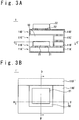
- the predetermined region (the space) 50 may be a closed space as shown in FIG. 2A and FIG. 2B , and may be an opened region (the space) as shown in FIG. 3A and FIG. 3B.
- FIG. 3A and FIG. 3B are sectional views schematically showing another configuration example of the multichip module according to the present embodiment.
- FIG. 3A is a vertical sectional view along the DD' line in FIG. 3B
- FIG. 3B is a horizontal sectional view along the CC' line in FIG. 3A .
- semiconductor substrate sections 11A" to 11D" as a part of the semiconductor substrates 11A to 11D are omitted, compared with the multichip module 1.
- the multichip module 1' includes semiconductor substrates 11A' to 11D' and provides the region (the space) 50 having an opening. The effect like the multichip module 1 can be attained even in this case.
- the predetermined region (the space) 50 is opened to a predetermined direction.
- the multichip module 1' may have the predetermined region opened into plural directions.
- end sections of semiconductor substrates opposite to the open end (substrate ends 11A" to 11D") of the region 50 through the semiconductor chip 21 may be cut or omitted.
- the outward form of the predetermined region (the space) 50 has a rectangular parallelepiped shape, but may have another shape. For example, as another shape, it is exemplified by a column shape.
- FIG. 4 is a block diagram schematically showing a configuration example of the on-board computer according to the present embodiment.
- the on-board computer 10 contains a multichip module 1 mounted on the mount substrate 4, an external interface (I/F) 2 and a power supply 3.
- the multichip module 1 is as mentioned above, and contains the semiconductor chip 22 as the CPU and the semiconductor chip 21 as the memory at least.
- the external interface 2 is an input/output unit which inputs and outputs data between the multichip module 1 and an external unit.
- the power supply 3 supplies electric power to the multichip module 1 and the external interface 2.
- the on-board computer 10 configures a computer from the CPU (the semiconductor chip 22), the memory (the semiconductor chip 21) and the input/output unit (the external interface 2).
- the on-board computer 10 according to the present invention is used as an interface substrate (calling an interface board or an extension card). Specifically, by mounting one of the semiconductor chips 21 and 22 as a sensor and the other as ASIC for data read, the on-board computer 10 functions as a sensor interface substrate.
- FIG. 5 is a partial sectional view schematically showing a configuration example of the on-board computer according to the present embodiment.
- FIG. 5 is a sectional view along the EE' line in FIG. 4 .
- the multichip module 1 is connected with the mount substrate 4 by the flip chip bonding. That is, a pad (connected with a wiring line passing through the semiconductor substrate 11A) on the undersurface of the semiconductor substrate 11A and a pad (connected with a wiring line on the mount substrate 4) on the upper surface of the mount substrate 4 are connected through a bump (gold, solder, etc.) 5.
- the method of mounting the multichip module 1 on the mount substrate 4 may be carried out by wire bonding.
- the on-board computer 10 uses the multichip module 1 according to the present embodiment, the downsizing, high-density implementation and lighting become possible.
- the high functionality, superior performance, downsizing and lightening of the satellite become possible while maintaining the size of the whole satellite.
- FIG. 6 to FIG. 12 are sectional views schematically showing the multichip module manufacturing method according to the present embodiment.
- the plurality of semiconductor substrates 11A to 11D are prepared.
- the plurality of semiconductor substrates 11A to 11D may be manufactured by a conventionally known method. For example, the following methods are proposed.
- Electronic devices, wiring line layers and metal electrodes (pads) are formed in a surface region of one of the planes (hereinafter, to be referred to as a first plane) of a silicon substrate 40A.
- the surface of the first plane is covered with a flattened insulating layer and the metal electrodes are partially exposed.
- the first surface is adhered to a glass support substrate, and a surface opposite to the first surface (the other surface of the silicon substrate 40A) is polished to make the silicon substrate 40 thin.
- the substrate 40A is exposed in the polished surface (hereinafter, to be referred to as the second surface).
- the silicon substrate 40A is etched in a position of the second surface corresponding to the position of the metal electrode on the first surface to form a via-hole to pass from the second surface to the metal electrode of the first surface.
- an insulating film e.g. SiO 2
- the insulating film in the bottom of the via-hole is etched to expose the metal electrode of the first surface in the bottom of the via-hole.
- a barrier film e.g. TiN
- a metal film e.g. Cu
- the metal film on the second surface is polished with a CMP process to expose the second surface.
- a via-contact (via) of the metal film is completed in the via-hole.
- the substrate 40A of the second surface is etched to become thin for the top part of the via-contact to protrude from the second surface slightly.
- an insulating film e.g. SiO 2
- the insulating film e.g. SiO 2
- the insulating film is removed from the top part of the via-contact by etching to expose the top part of the via-contact.
- a wiring line and a metal electrode (the pad) are formed in the insulating film according to need.
- via-contacts 41A and 42A as the wiring lines passing through the substrate 40A, and a metal electrode 43A connected with the via-contact 42A through the wiring line and a wiring line (not shown) are formed in the semiconductor substrate 11A.
- the glass substrate adhered to the first surface is removed.
- a wiring line layer can be formed in the semiconductor substrate as described below. That is, after the insulating film is formed by thermal oxidation and so on on the whole surface of the silicon wafer in which through holes are formed by etching exemplified by DeepRIE (Deep Reactive Ion Etching), Cu passing-through wiring lines and son on are formed by Cu embedding.
- DeepRIE Deep Reactive Ion Etching
- the method of forming a semiconductor substrate 11B is same as a case of the semiconductor substrate 11A. Moreover, a process of forming a predetermined region (a space) 50B is added. That is, before and after the process of forming a via-hole or at the same time as the above process, a process of forming a predetermined region (the space) 50B is carried out. Specifically, the substrate 40A in the position of the predetermined region (the space) 50B is etched to form a space (a hole) which reaches the first surface from the second surface. The space (the hole) functions as the predetermined region (the space) 50B. For example, the etching to such a relatively large region can be realized by using the technique of an MEMS manufacture.
- a frame-like passing-through ditch 201 is formed on the semiconductor substrate 11 by the etching exemplified by DeepRIE.
- an inside region 202 in the passing-through ditch 201 from the semiconductor substrate 11 is excluded.
- the predetermined region (the space) 50 is formed.
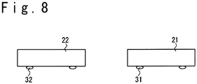
- the plurality of semiconductor chips 21 and 22 are prepared as shown in FIG. 8 .
- a memory in the condition of a die (bare chip) is prepared as the semiconductor chip 21 and a CPU in the condition of a die (bare chip) is prepared as the semiconductor chip 22.
- they may be a memory and a CPU in the condition of the package.
- the semiconductor chip 21 is a memory and the semiconductor chip 22 is the CPU.
- an optional chip may be used in addition to this.
- the semiconductor chip 21 which is provided in the predetermined region (the space) 50 may be a CPU
- the semiconductor chip 22 which is provided on the semiconductor substrate 11D may be a memory.
- the semiconductor substrate 11B is bonded with the semiconductor substrate 11A by the room-temperature bonding method as shown in FIG. 9 .
- one of the surfaces of the semiconductor substrate 11A and one of the surfaces of the semiconductor substrate 11B are bonded such that the predetermined via-contacts 41A and 41B set previously for connection are connected.
- an electrode to connect the via-contact and the substrate may be connected electrically or the electrode may leave.
- the semiconductor chip 21 is mounted (arranged) on the semiconductor substrate 11A in the predetermined region (the space) 50 as shown in FIG. 10 .
- the metal electrode 43A of the semiconductor substrate 11A and a bump (gold, solder, etc.) 31 of the semiconductor chip 21 are connected in the flip chip method.
- an under fill material 33 may be filled between the semiconductor substrate 11A and the semiconductor chip 21.
- the semiconductor substrate 11C is bonded with the semiconductor substrate 11B which has been bonded with the semiconductor substrate 11, by the room-temperature bonding method.
- the other surface of the semiconductor substrate 11B and one of the surfaces of the semiconductor substrate 11C are bonded such that the predetermined via-contacts 41B and 41C set previously for the connection are connected.
- a method disclosed in Japanese Patent No. 3970304 is exemplified as the room-temperature method.
- the predetermined region (the space) 50 is formed on the semiconductor substrate 11A to be surrounded by the semiconductor substrates 11B and 11C.
- the semiconductor substrate 11D is bonded to the semiconductor substrate 11C by the room-temperature bonding method as shown in FIG. 12 .
- one of the surfaces of the semiconductor substrate 11D and the other surface of the semiconductor substrate 11C are bonded such that predetermined via-contact 41C and via-contact 41D which are previously set for connection are connected.
- the room-temperature bonding method a technique disclosed in Japanese Patent No. 3970304 is exemplified.
- the predetermined region (the space) 50 is formed on the semiconductor substrate 11A to be surrounded by the semiconductor substrates 11B, 11C and 11D
- the semiconductor chip 22 is mounted (arranged) on the semiconductor substrate 11D as shown in FIG. 13 .
- a metal electrodes 43D of the semiconductor substrate 11D and bumps (gold, solder, etc.) 32 of the semiconductor chip 22 are connected by the flip chip method.
- under fill material 34 may be filled between the semiconductor substrate 11D and the semiconductor chip 22.
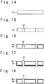
- a silicon substrate 40 is prepared on which an electronic device and a wiring line layer are formed in the surface region of the first surface. In this case, it is desirable to polish a second surface of the silicon substrate in order to make it thin. Note that the silicon substrate 40 may not have the electronic device and the wiring line layer formed.
- the via-hole 30 is formed to connect the first surface and the second surface in the silicon substrate 40.
- the via-hole 30 is provided in a predetermined position of the silicon substrate 40 by DeepRIE (Deep Reactive Ion Etching).
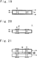
- an insulating film 44 (e.g. SiO 2 ) is formed to cover the whole surface of silicon substrate 40 (the first surface, the second surface and side surfaces) and the inner wall of the via-hole 30.
- a barrier film (e.g. TiN) (not shown) is formed on the surface of the insulating film 44 by, for example, a sputtering method, and then a metal film is embedded in the via-hole 30.
- a Cu film 45 is formed on the second surface and embedded in the via-hole 30.
- the Cu 45 film may be plated directly on the barrier film.
- a Cu seeding layer (e.g. Cu/Ti) may be formed on the barrier film and the Cu film 45 may be plated on the Cu seeding layer.
- the Cu film 45 formed on the second surface and the first surface is removed by polishing which is exemplified by CMP, to expose and flatten the first surface and the second surface.
- CMP polishing which is exemplified by CMP
- a metal film is formed on the first surface and the second surface by depositing (or sputtering). It is desirable that the outermost surface of the metal film is formed of an Au film 46 from the viewpoint of the conductivity. Also, it is desirable that a Ti film 47 is formed between the insulating film 44 and the Au film 46 to improve the adhesion of the insulating film 44 and the Au film 46. In an example shown in FIG. 19 , the Ti film 47 and the Au film 46 are formed in order on the insulating film 44 and the via-contact 41 in the first surface and the second surface, to form an Au/Ti metal film.
- a wiring line pattern (not shown) is formed on the Au film 46 in the first surface and the second surface by, for example, a Ti mask, and an Au/Ti metal electrode 43 and wiring lines (not shown) are formed by a dry etching method.
- the semiconductor substrate 11 is formed which contains the via-contact 41 formed of Cu, and the metal electrode 43 formed of the Au/Ti metal film, and the wiring lines (not shown).
- a plurality of silicon substrates 11 formed as mentioned above are bonded and is implemented as a multichip module.
- the semiconductor substrate 11A and the semiconductor substrate 11B are bonded through a metal electrode 43A and a metal electrode 43B by the room-temperature bonding method.
- the space 60 is generated between the surfaces of the semiconductor substrate 11A and the semiconductor substrate 11B opposing to each other.
- the height depends on the metal electrode 43 and is as small as the several nanometers.
- the space 60 becomes vacuum if the periphery of the space 60 is surrounded by the metal wiring lines 43A and 43B connected to each other.
- the space 60 may be filled with an oxide film.
- the oxide film is formed on the first surface and the second surface of the semiconductor substrate 11 shown in FIG. 20 .
- the metal electrode 43 and wiring lines (not shown) are exposed through a flattening process.
- the oxide film is formed to have the height of the same surface as the surface of metal wiring line 43.
- the structure of the metal electrode 43 to be formed here is not limited to this structure and the composition and the number of layers can be selected optionally such as the Au/Ni/Ti metal film and the Au/Pt/Ti metal film.
- the electrode damaging due to the heat can be prevented.
- the surface mounting part 25 is exemplified by any of the semiconductor chips 21 and 22, and semiconductor chips 23 and 24 or chip parts 71 and 72, to be described later, and an electronic part of a chip shape mountable on the semiconductor substrate 11.
- the Ti film 47, the Ni film 48 and the Au film 46 are formed in order on the via-contact 41 and the insulating film 44 of the first surface and and the second surface by, for example, sputtering, to form the Au/Ni/Ti metal film.
- a wiring line pattern (not shown) by, for example, the Ti mask is formed on the Au films 46 of the first surface and the second surface, to form the Au/Ni/Ti metal electrode 43 and the wiring lines (not shown) by a dry etching.
- the semiconductor substrate 11 is formed to contain the via-contact 41 formed of Cu, and the metal electrode 43 formed from the Au/Ni/Ti metal film, and the wiring lines (not shown).
- the plurality of silicon substrates 11 manufactured as mentioned above are bonded to be implemented as the multichip module.
- the semiconductor substrate 11A and the semiconductor substrate 11B are bonded through the metal electrode 43A and the metal electrode 43B by the room-temperature bonding method.
- the space 60 is formed between the surfaces of the semiconductor substrate 11A and the semiconductor substrate 11B opposing to each other and the height is several-nm order.
- the space 60 may be filled with the insulating film.
- the metal electrode 43 of the present embodiment contains Ni having high heat resistance, the heat damaging does not occur even if the surface mounting part 25 is connected through the solder 70. That is, in the multichip module 1 of this example, the surface mounting part 25 can be mounted on the semiconductor substrate 11 by soldering. Also, in the present embodiment, an example that the surface mounting part 25 is soldered through lead lines is shown, but the present embodiment is not limited to this. An example is effective where the electrodes on the surface of surface mounting part 25 and the metal electrodes 43 are connected through solder bumps.
- the wiring line material is not limited to the example, and Al wiring lines may be used.
- Al films 49 are formed on the via-hole 30 and the insulating films 44 of the first surface and the second surface by a sputtering.
- a via-contact 41' is formed to connect the first surface and the second surface by the Al film 49 formed on the via-hole 30.
- a wiring line pattern (not shown) is formed on the Al films 49 of the first surface and the second surface by the Ti mask, and the Al metal electrode 43' and the wiring lines (not shown) are formed by dry etching.
- the semiconductor substrate 11' is formed to contain the via-contact 41', the metal electrode 43' and the wiring lines (not shown) which are formed from the Al film 49.
- the plurality of silicon substrates 11' formed as mentioned above are bonded as in the above-mentioned silicon substrate 11 and the bonded substrates are implemented as a multichip module.
- the semiconductor substrate 11A' and the semiconductor substrate 11B' are bonded through metal electrodes 43A' and metal electrodes 43B' by the room-temperature bonding method.
- the space 60 is produced between the surfaces of the semiconductor substrate 11A and the semiconductor substrate 11B opposing to each other and the height is several-nm order.
- the space may be filled with the insulating film.
- the structure of the metal electrode 43' to be formed is not limited to this, and for example, the Au film 62 may be formed on the surface of the Al film 49 to improve conductivity.
- the Ti film 61 is formed between the Al film 49 and the Au film 62, in order to improve fitness with the Al film 49, as shown in FIG. 29 .
- the metal film formed on the Al film 49 can be selected optionally in composition and the number of layers, such as the Au/Ni/Ti metal film and the Au/Pt/Ti metal film as mentioned above.
- the multichip module according to the present embodiment is manufactured in this way.
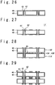
- the manufacturing method of the multichip module of FIG. 14 to FIG. 28 is only an example, and the present embodiment is not limit to this example.
- the via-hole 30 is provided to pass through silicon substrate 40 from the first surface to the second surface.
- the via-hole may not pass through the silicon substrate 40.
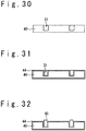
- the via-contact (via) 42 may be formed as shown in FIG. 30 to FIG. 32 .
- the via-hole 31 is provided in a predetermined position on the first surface of the silicon substrate 40 by DeepRIE.
- the via-hole 31 may be a hole with a predetermined depth from the first surface and is not necessary to pierce to the second surface.
- the insulating film 44 (e.g. SiO 2 ) is formed to cover the whole surface of the silicon substrate 40 (the first surface, the second surface and the side planes) and the inner wall of the via-hole 31.
- a barrier film e.g. TiN
- a metal film is embedded in the via-hole 31.
- a Cu film 45 is embedded in the via-hole 31 by a Cu electrolysis plating method.
- the Cu film 45 may be plated directly on the barrier film.
- a Cu seeding layer e.g. Cu/Ti
- the Cu film 45 may be plated on the Cu seeding layer.
- the Cu film 45 formed on the first surface and the second surface are removed by polishing which is exemplified by a CMP, and the first surface and the second surface are exposed to flatten.
- the via-contact 41 in which the Cu film 45 is embedded is formed.
- the via-contact 41 can be formed by using the via-hole 31 which does not pierce from the first surface of the silicon substrate 40 to the second surface.
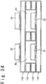
- FIG. 32 to FIG. 37 are sectional views schematically showing modification examples of the configuration of the multichip module according to the present embodiment.
- the semiconductor substrates 11E, 11F, and 11G are stacked on the multichip module 1 of FIG. 2A .
- the semiconductor substrates 11E, 11F, and 11G have the almost same configuration as the semiconductor substrates 11B, 11C and 11D, respectively basically.
- the semiconductor substrates 11E and 11F are stacked on the semiconductor substrate 11D to surround the semiconductor chip 22 (surround a predetermined region (space) 51).
- the semiconductor substrate 11G is stacked on the semiconductor substrate 11F to cover above the semiconductor chip 22 (to cover the predetermined region 51).
- the semiconductor substrate and the semiconductor chip are stacked in further upward direction by the same method.
- the predetermined region (space) 51 is provided for the multichip module 1 of FIG. 2A , and the semiconductor chip 23 as the surface mounting part is mounted (arranged) there.
- Such a configuration can be realized by carrying out etching to form a separate predetermined region (space) 51 to the semiconductor substrates 11B and 11C, simultaneously with the etching to form the predetermined region (space) 50.
- the semiconductor chip 24 may be mounted (arranged) on the semiconductor substrate 11D.
- the semiconductor chip 23 is mounted (arranged) in the predetermined region (space) 50 of the multichip module 1 of FIG. 2A .
- Such a configuration can be realized by extending the predetermined region when carrying out etching to the semiconductor substrates 11B and 11C to form the predetermined region (space) 50.
- the semiconductor chip 24 s the surface mounting part may be mounted (arranged) on the semiconductor substrate 11D.
- the multichip module of the present embodiments may be a multichip module in which all or part of the configurations of the multichip modules of FIG. 2A, FIG. 2B , FIG. 3A, FIG. 3B and FIG. 33 to FIG. 35 are combined.
- the multichip module 1 on which the semiconductor chips 21 to 24 are mounted is shown as examples.
- the embodiment is not limit to this.
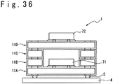
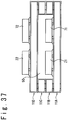
- the multichip module 1 according to the present invention may be mounted with chip parts 71 and 72 as the surface mounting parts in place of the semiconductor chips 21 to 24.
- the chip parts 71 and 72 are passive components with a chip shape exemplified by a chip resistor, a chip condenser, and a chip inductor.
- FIG. 36 and FIG. 37 An example of mounting the chip parts 71 and 72 on the multichip module 1 according to the present invention is shown in FIG. 36 and FIG. 37 .
- the chip parts 71 and 72 are mounted on the multichip module 1 in place of the semiconductor chips 21 and 22 shown in FIG. 2A .
- the semiconductor chips 21 and 22 and the chip parts 71 and 72 may be mixedly mounted on the multichip module 1.
- the chip part may be mounted in place of the semiconductor chips 21 to 24 as shown in FIG. 3A , FIG. 33 , FIG. 34 , and FIG. 35 , and the semiconductor chip and the chip part may be mixedly mounted.
- the above-mentioned embodiments may be combined in a range without technical contradiction. Note that the number of surface mounting part, and the kind, size and arrangement position of the surface mounting part mounted on the multichip module 1 can be optionally set.
- the multichip module of the present embodiment adopts a semiconductor substrate (e.g. silicon substrate) as a mount substrate but does not use the substrate made of resin and the substrate made from ceramic.
- the wiring lines according to a wiring line rule of the semiconductor substrate can be used as the wiring line of the mount substrate.
- the wiring line can be miniaturized, the area of the wiring line to be occupied in the mount substrate can be reduced, and the mount substrate can be downsized and be made in a high density.
- the multilayer configuration of the semiconductor substrates e.g. silicon substrates
- an IC chip is embedded in the inside of the multilayer configuration.
- the multichip module 1 in which a CPU is mounted can be configured to the height direction three-dimensionally.
- the base area of the multichip module can be reduced without changing the area of the whole mount substrate.
- the area required to arrange the multichip module can be reduced to the area of the semiconductor substrate 11A (for one) is the multichip module takes without changing the areas of the semiconductor substrates 11A to 11D (for four).
- the multichip module can be remarkably downsized and made in a high density.
- a semiconductor substrate e.g. silicon
- it is predominant in the viewpoint of the thermal radiation design of a part (e.g. semiconductor chip like the CPU) because the heat conduction is better compared with a substrate made from resin and a substrate made from ceramics.
- a semiconductor chip is embedded inside the stack configuration of a plurality of semiconductor substrates (e.g. silicon substrates). Therefore, theoretically, there is no limitation of stacking in the height direction with respect to the multichip module, and very many semiconductor substrates can be stacked. Therefore, a super-high-density CPU module can be realized. Also, because the plurality of semiconductor substrates (e.g. silicon substrates) are bonded by the room-temperature bonding, a heat load is never applied to the surface mounting part exemplified by an IC chip. Therefore, there is no fear of breaking the surface mounting part exemplified by the IC chip in assembling step and the yield is improved.
- semiconductor substrates e.g. silicon substrates
- the multichip module of the present embodiment is suitable especially for the multichip module having a sensor function and an analog function in addition to a digital function.
- the present invention is suitable especially for a multichip module dealt with in HIC and MCM and difficult to deal with in SOC like a case of combining a digital IC and a sensor IC and an analog IC.
- the on board computer of the present embodiment using these multichip modules can achieve the similar effect.
- the CPU and the peripheral IC can be made three-dimensionally through the implementation using a room-temperature bonding technique, compared with the substrate on which a conventional CPU is mounted.
- the multichip module and the on board computer can be remarkably downsized and can be formed in a high density.
- the present invention is predominant in point of the thermal radiation design of a part (CPU) because the module is better in the heat conduction, compared with a substrate made from resin and a substrate made from ceramics.
- a mounted chip is not limited to an IC chip and a memory chip.
- the mounted chip may include a chip (MEMS: Micro Electro Mechanical Systems) having a machine element such as a sensor and an actuator.
- MEMS Micro Electro Mechanical Systems
- the multichip module can be called a MEMS module.
Landscapes
- Internal Circuitry In Semiconductor Integrated Circuit Devices (AREA)
- Engineering & Computer Science (AREA)
- Manufacturing & Machinery (AREA)
Abstract
Description
- The present invention related to a multichip module, an on board computer and a multichip module manufacturing method. Especially, the present invention relates to a multichip module, an on board computer, a sensor interface substrate and a multichip module manufacturing method, which are for an electronic equipment in which downsizing and lightening are required.
- The downsizing and lightening of the electronic equipment are requested. Especially, in a small satellite, it is strongly required to achieve high functionality, high performance, downsizing and lightening of a satellite while maintaining the size of the satellite. Therefore, it is necessary to further carry out downsizing and high density mounting even in an electronic device such as an information processing apparatus mounted in the satellite. It is possible to cope with the downsizing of the information processing apparatus to an extent by the technique such as SOC (System On Chip), HIC (Hybrid IC), and MCM (Multi-Chip Module).
-
FIG. 1 is a side view schematically showing a configuration example of a conventional MCM. The MCM 101 contains amount substrate 110, anIC package 111, anIC package 112 andwiring lines 113. TheIC package 111 and theIC package 112 contain asemiconductor chip 121 and asemiconductor chip 122, respectively. Themount substrate 110 is a circuit board made from ceramic or resin. For example, thesemiconductor chips wiring lines 113 provided inside thesubstrate 110 and on the surface of thesubstrate 110 connect theIC packages wiring line 113 is wide (the minimum width of about 200 µm) and it needs to secure an area necessary for the wiring lines. Therefore, thesubstrate 110 cannot be made small. For this reason, it is difficult that the downsizing and lightening of theMCM 101 are dealt with. - As the related techniques, in
JP 2012-529770A WO2010/151350 ) discloses a method of providing a multichip package and inter-connection from a die to a die in the multichip package. The multichip package contains a substrate, a first die, a second die and a bridge. The substrate has a first surface, a second surface opposite to it, and a third surface extending from the first surface to the second surface. The first die and the second die are mounted on the first surface of the substrate. The bridge is mounted on the first die and the second die adjacent to the third surface of the substrate. Any part of the substrate does not exist under the bridge. The bridge connects the first die and the second die. - In this prior art, there is a case that the second die is mounted on the first die mounted on the substrate (there is a case that the bridge is the die). In such a case, the wiring line of the second die mounted on the upper side needs to pass through the first die mounted on the lower side. Therefore, it would be a restriction of height when mounting the dies in a height direction.
- The technique of room-temperature bonding which can bond semiconductor substrates at the normal temperature is disclosed in
Japanese Patent 2,791,429B Japanese Patent 3,970,304B JP 2003-318219A -
- [Patent Literature 1]
JP 2012-529770A - [Patent Literature 2]
JP 2791429B - [Patent Literature 3]
JP 3970304B - [Patent literature 4]
JP 2003-318219A - An object of the present invention is to provide a multichip module, an on board computer, and a method of manufacturing a multichip module, in which the downsizing and lightening are possible while maintaining a performance. Another object of the present invention is to provide a multichip module, an on board computer and a multichip module manufacturing method, in which there is no limitation of the number of stacked layers theoretically while maintaining a performance.
- The above objects, objects except for the above objects and benefits of the present invention can be easily understood from the following description and the attached drawings.
- A multichip module of the present invention includes a plurality of semiconductor substrates and a plurality of surface mounting parts. The plurality of semiconductor substrates each have a wiring line region which contains a wiring line to pierce from one of the surfaces of the substrate to the other surface. The plurality of surface mounting parts are mounted on either of the plurality of semiconductor substrates. The plurality of semiconductor substrates are stacked to form a multilayer structure. A first surface mounting part as at least one of the plurality of surface mounting parts is arranged and mounted in the inside region of the multilayer structure.
- Because such a multichip module uses the semiconductor substrate as a mount substrate, the wiring line determined according to a wiring line rule of the semiconductor substrate can be used as the wiring line of the mount substrate. Thus, the wiring line can be miniaturized and the wiring line region to be occupied on the mount substrate can be reduced. In addition, the surface mounting part and the mount substrate can be structured in the height direction three-dimensionally. In this way, an area required to mount the multichip module without changing the whole area of the mount substrate can be reduced. Thus, it becomes possible to remarkably downsize and lighten the multichip module and make the multichip module to a high-density. Also, because a semiconductor substrate can be used as the mount substrate, the present invention is predominant in the viewpoint of the radiation design, because the heat conduction is better, compared with a substrate made from resin and a substrate made from ceramics.
- An on board computer of the present invention includes a multichip module and an interface. The multichip module is mounted on a mount substrate, and contains a CPU and a memory as surface mounting parts. The interface inputs and outputs data of the multichip module.
- Because such an on board computer uses the above-mentioned multichip module, the downsizing, the lightening and the high-density mounting can be realized.
- A multichip module manufacturing method of the present invention includes preparing a first semiconductor substrate, a second semiconductor substrate and a third semiconductor substrate, which each have a wiring line region which contains a wiring line to pierce from one of the surfaces to the other surface. The second semiconductor substrate is stacked and bonded on the first semiconductor substrate by a room-temperature bonding method. A first surface mounting part is mounted on a part of the first semiconductor substrate where it is not covered with the second semiconductor substrate. The third semiconductor substrate is stacked and bonded on the second semiconductor substrate by the room-temperature bonding method to cover the first surface mounting part.
- In such a multichip module manufacturing method, the plurality of semiconductor substrates are stacked by the room-temperature bonding method. Therefore, a heat load is never applied to a surface mounting part upon stacking. Therefore, there is no fear that a surface mounting part is broken in an assembling step, and the yield is improved. Also, the manufactured multichip module has the above-mentioned configuration and can realize downsizing, lightening and high-density mounting and so on.
- By the present invention, it is possible to provide the multichip module, the on board computer and the multichip module manufacturing method, in which the downsizing and the lightening are possible while maintaining a performance. Also, it is possible to provide the multichip module, the on board computer and the multichip module manufacturing method, in which there is no limitation of the number of layers theoretically while maintaining a performance.
- The objects, effects, and features of the above invention would become clear from the description of the embodiments in cooperation with the attached drawings.
- [
FIG. 1 ]
FIG. 1 is a side view schematically showing a configuration example of a conventional MCM. - [
FIG. 2A ]
FIG. 2A is a vertical sectional view schematically showing a configuration example of a multichip module according to an embodiment. - [
FIG. 2B ]
FIG. 2B is a horizontal sectional view schematically showing the configuration example of the multichip module according to the embodiment. - [
FIG. 3A ]
FIG. 3A is a vertical sectional view schematically showing another configuration example of the multichip module according to an embodiment. - [
FIG. 3B ]
FIG. 3B is a horizontal sectional view schematically showing the other configuration example of the multichip module according to the embodiment. - [
FIG. 4 ]
FIG. 4 is a block diagram schematically showing a configuration example of the on board computer according to the embodiment. - [
FIG. 5 ]
FIG. 5 is a partial sectional view schematically showing a configuration example of the on board computer according to an embodiment. - [
FIG. 6 ]
FIG. 6 is a sectional view schematically showing a multichip module manufacturing method according to an embodiment. - [
FIG. 7A ]
FIG. 7A is a plan view schematically showing the multichip module manufacturing method according to an embodiment. - [
FIG. 7B ]
FIG. 7B is a plan view schematically showing the multichip module manufacturing method according to the embodiment. - [
FIG. 8 ]
FIG. 8 is a sectional view schematically showing the multichip module manufacturing method according to the embodiment. - [
FIG. 9 ]
FIG. 9 is a sectional view schematically showing the multichip module manufacturing method according to an embodiment. - [
FIG. 10 ]
FIG. 10 is a sectional view schematically showing the multichip module manufacturing method according to the embodiment. - [
FIG. 11 ]
FIG. 11 is a sectional view schematically showing the multichip module manufacturing method according to the embodiment. - [
FIG. 12 ]
FIG. 12 is a sectional view schematically showing the multichip module manufacturing method according to an embodiment. - [
FIG. 13 ]
FIG. 13 is a sectional view schematically showing the multichip module manufacturing method according to the embodiment. - [
FIG. 14 ]
FIG. 14 is a sectional view schematically showing the multichip module manufacturing method according to an embodiment. - [
FIG. 15 ]
FIG. 15 is a sectional view schematically showing the multichip module manufacturing method according to the embodiment. - [
FIG. 16 ]
FIG. 16 is a sectional view schematically showing the multichip module manufacturing method according to the embodiment. - [
FIG. 17 ]
FIG. 17 is a sectional view schematically showing the multichip module manufacturing method according to the embodiment. - [
FIG. 18 ]
FIG. 18 is a sectional view schematically showing the multichip module manufacturing method according to the embodiment. - [
FIG. 19 ]
FIG. 19 is a sectional view schematically showing the multichip module manufacturing method according to the embodiment. - [
FIG. 20 ]
FIG. 20 is a sectional view schematically showing the multichip module manufacturing method according to the embodiment. - [
FIG. 21 ]
FIG. 21 is a sectional view schematically showing the multichip module manufacturing method according to the embodiment. - [
FIG. 22 ]
FIG. 22 is a sectional view schematically showing the multichip module manufacturing method according to the embodiment. - [
FIG. 23 ]
FIG. 23 is a sectional view schematically showing the multichip module manufacturing method according to the embodiment. - [
FIG. 24 ]
FIG. 24 is a sectional view schematically showing the multichip module manufacturing method according to the embodiment. - [
FIG. 25 ]
FIG. 25 is a sectional view schematically showing the multichip module manufacturing method according to the embodiment. - [
FIG. 26 ]
FIG. 26 is a sectional view schematically showing the multichip module manufacturing method according to the embodiment. - [
FIG. 27 ]
FIG. 27 is a sectional view schematically showing the multichip module manufacturing method according to the embodiment. - [
FIG. 28 ]
FIG. 28 is a sectional view schematically showing the multichip module manufacturing method according to the embodiment. - [
FIG. 29 ]
FIG. 29 is a sectional view schematically showing the multichip module manufacturing method according to the embodiment. - [
FIG. 30 ]
FIG. 30 is a sectional view schematically showing the multichip module manufacturing method according to an embodiment. - [
FIG. 31 ]
FIG. 31 is a sectional view schematically showing the multichip module manufacturing method according to the embodiment. - [
FIG. 32 ]
FIG. 32 is a sectional view schematically showing the multichip module manufacturing method according to the embodiment. - [
FIG. 33 ]
FIG. 33 is a sectional view schematically showing a modification example of the configuration of the multichip module according to an embodiment. - [
FIG. 34 ]
FIG. 34 is a sectional view schematically showing the modification example of the configuration of the multichip module according to the embodiment. - [
FIG. 35 ]
FIG. 35 is a sectional view schematically showing the modification example of the configuration of the multichip module according to the embodiment. - [
FIG. 36 ]
FIG. 36 is a sectional view schematically showing the modification example of the configuration of the multichip module according to the embodiment. - [
FIG. 37 ]
FIG. 37 is a sectional view schematically showing the modification example of the configuration of the multichip module according to the embodiment. - Hereinafter, a multichip module, an on board computer and a multichip module manufacturing method according to embodiments of the present invention will be will be described with reference to the attached drawings.
- The configuration of the multichip module according to an embodiment will be described.
FIG. 2A and FIG. 2B are sectional views schematically showing a configuration example of the multichip module according to the present embodiment. Here,FIG. 2A is the vertical sectional view along the BB' line inFIG. 2B and FIG. 2B is the horizontal sectional view along the AA' line inFIG. 2A . Themultichip module 1 contains a plurality ofsemiconductor substrates semiconductor chips - Each of the plurality of
semiconductor substrates semiconductor substrates semiconductor substrates semiconductor substrates - Each of the plurality of
semiconductor chips semiconductor chips semiconductor chip 21 is a memory and thesemiconductor chip 22 is a CPU. Thesemiconductor chip 21 is arranged (mounted) on thesemiconductor substrate 11A, and is connected by flip-chip bonding. That is, a pad (connected with an internal circuit) on the undersurface of thesemiconductor chip 21 and a pad (connected with a wiring line region) on the upper surface of thesemiconductor substrate 11A are connected through a bump (gold, solder, etc.) 31. In the same way, thesemiconductor chip 22 is arranged (mounted) on thesemiconductor substrate 11D, and is connected by the flip chip bonding. That is, a pad (connected with an internal circuit) on the undersurface of thesemiconductor chip 22 and a pad (connected with the wiring line region) on the surface of thesemiconductor substrate 11D are connected through a bump (gold, solder, etc.) 32. In this way, a semiconductor chip is connected with another semiconductor chip through the wiring lines of the wiring line region provided in the semiconductor substrate. - The
semiconductor substrate 11A has thesemiconductor chip 21 arranged (mounted) on one surface. Thesemiconductor substrate 11B is arranged on thesemiconductor substrate 11A on the same side as thesemiconductor chip 21. In other words, thesemiconductor substrate 11B is stacked on thesemiconductor substrate 11A to surround the periphery of thesemiconductor chip 21 away from the semiconductor chip 21 (surround a predetermined region 50). Thesemiconductor substrate 11C is arranged on thesemiconductor substrate 11B on the same side as thesemiconductor chip 21. In other words, thesemiconductor substrate 11C is stacked on thesemiconductor substrate 11B to surround the periphery of the semiconductor chip 21 (surround the predetermined region 50). Thesemiconductor substrate 11D is arranged to cover the semiconductor chip 21 (to cover the predetermined region 50) so that thesemiconductor substrate 11D is stacked on thesemiconductor substrate 11C. That is, the predetermined region 50 (a predetermined space) is a region provided inside the stackedsemiconductor substrates 11A to 11D (formed by thesemiconductor substrates 11A to 11D). Thesemiconductor chip 21 is arranged in thepredetermined region 50. Therefore, thesemiconductor chip 21 is arranged inside the stackedsemiconductor substrates 11A to 11D. On thesemiconductor substrate 11D, thesemiconductor chip 22 is mounted. Note that in the present embodiment, thesemiconductor chip 22 is mounted on thesemiconductor substrate 11D. However, the present invention is not limited to this, and thesemiconductor chip 22 may be not mounted on thesemiconductor substrate 11D. - Note that the
semiconductor substrate 11C may be integrated with thesemiconductor substrate 11B to form a unitary body. Also, when the thickness of the semiconductor chip 21 (containing the thickness of bump 31) is sufficiently thinner than the thickness of thesemiconductor substrate 11B, thesemiconductor substrate 11C may be eliminated. Also, the semiconductor chips 21 and 22 may be an IC chip package. The number of semiconductor substrates and the number of semiconductor chips are not limited to the above example (four semiconductor substrates and two semiconductor chips), and these may be more or less, to be described later. - In this way, the
multichip module 1 according to the present embodiment has the configuration of multilayer configuration (three-dimensional configuration) in which the plurality ofsemiconductor substrates 11A to 11D are stacked. The semiconductor chip (die) 21 is embedded in the multilayer configuration (the three-dimensional configuration) (thesemiconductor chip 21 is arranged in the predetermined region 50) to realize the three-dimensional implementation. Each of the semiconductor chips is connected with another semiconductor chip through wiring lines (wiring line layers, passing wiring lines) in the wiring line region provided for the semiconductor substrate. Therefore, as far as there is room in the space in a height direction, theoretically, there is not a limit in the number of layers stacked in the height direction. In addition, the wiring line regions of the plurality ofsemiconductor substrates 11A to 11D can be formed by using the micro-fabrication process of the semiconductor integrated circuit. That is, the wiring lines and the electronic devices can be manufactured finely. Thus, it becomes possible to carry out the downsizing and high-density mounting of themultichip module 1. Also, when thesemiconductor substrates 11A to 11D as the mount substrates are silicon substrates, the heat conduction is better than a substrate made from resin and a substrate made from ceramics. Therefore, heat radiation of parts such as the semiconductor chips 21 and 22 (e.g. a CPU and a memory) are easy and the present embodiment is superior in the radiation design. - Note that in the
multichip module 1, the predetermined region (the space) 50 may be a closed space as shown inFIG. 2A and FIG. 2B , and may be an opened region (the space) as shown inFIG. 3A and FIG. 3B. FIG. 3A and FIG. 3B are sectional views schematically showing another configuration example of the multichip module according to the present embodiment. Here,FIG. 3A is a vertical sectional view along the DD' line inFIG. 3B and FIG. 3B is a horizontal sectional view along the CC' line inFIG. 3A . In a multichip module 1',semiconductor substrate sections 11A" to 11D" as a part of thesemiconductor substrates 11A to 11D are omitted, compared with themultichip module 1. The multichip module 1' includessemiconductor substrates 11A' to 11D' and provides the region (the space) 50 having an opening. The effect like themultichip module 1 can be attained even in this case. - Also, in the multichip module 1' shown in
FIG. 3 , the predetermined region (the space) 50 is opened to a predetermined direction. However, the multichip module 1' may have the predetermined region opened into plural directions. For example, in an example ofFIG. 3A and FIG. 3B , end sections of semiconductor substrates opposite to the open end (substrate ends 11A" to 11D") of theregion 50 through thesemiconductor chip 21 may be cut or omitted. Moreover, inFIG. 2A, FIG. 2B andFIG. 3A, and FIG. 3B , the outward form of the predetermined region (the space) 50 has a rectangular parallelepiped shape, but may have another shape. For example, as another shape, it is exemplified by a column shape. - Next, the configuration of the on-board computer (OBC) according to the present embodiment will be described.
FIG. 4 is a block diagram schematically showing a configuration example of the on-board computer according to the present embodiment. The on-board computer 10 contains amultichip module 1 mounted on themount substrate 4, an external interface (I/F) 2 and apower supply 3. Themultichip module 1 is as mentioned above, and contains thesemiconductor chip 22 as the CPU and thesemiconductor chip 21 as the memory at least. Theexternal interface 2 is an input/output unit which inputs and outputs data between themultichip module 1 and an external unit. Thepower supply 3 supplies electric power to themultichip module 1 and theexternal interface 2. In this way, the on-board computer 10 configures a computer from the CPU (the semiconductor chip 22), the memory (the semiconductor chip 21) and the input/output unit (the external interface 2). For example, preferably, the on-board computer 10 according to the present invention is used as an interface substrate (calling an interface board or an extension card). Specifically, by mounting one of the semiconductor chips 21 and 22 as a sensor and the other as ASIC for data read, the on-board computer 10 functions as a sensor interface substrate. -
FIG. 5 is a partial sectional view schematically showing a configuration example of the on-board computer according to the present embodiment. Here,FIG. 5 is a sectional view along the EE' line inFIG. 4 . In the on-board computer 10, themultichip module 1 is connected with themount substrate 4 by the flip chip bonding. That is, a pad (connected with a wiring line passing through thesemiconductor substrate 11A) on the undersurface of thesemiconductor substrate 11A and a pad (connected with a wiring line on the mount substrate 4) on the upper surface of themount substrate 4 are connected through a bump (gold, solder, etc.) 5. Note that the method of mounting themultichip module 1 on themount substrate 4 may be carried out by wire bonding. - In this way, because the on-
board computer 10 according to the present embodiment uses themultichip module 1 according to the present embodiment, the downsizing, high-density implementation and lighting become possible. By using such an onboard computer 10 as a computer for the satellite mounting, the high functionality, superior performance, downsizing and lightening of the satellite become possible while maintaining the size of the whole satellite. - Next, the multichip module manufacturing method according to the present embodiment will be described.
FIG. 6 to FIG. 12 are sectional views schematically showing the multichip module manufacturing method according to the present embodiment. - First, as shown in
FIG. 6 , the plurality ofsemiconductor substrates 11A to 11D are prepared. The plurality ofsemiconductor substrates 11A to 11D may be manufactured by a conventionally known method. For example, the following methods are proposed. - Electronic devices, wiring line layers and metal electrodes (pads) are formed in a surface region of one of the planes (hereinafter, to be referred to as a first plane) of a
silicon substrate 40A. The surface of the first plane is covered with a flattened insulating layer and the metal electrodes are partially exposed. Next, the first surface is adhered to a glass support substrate, and a surface opposite to the first surface (the other surface of thesilicon substrate 40A) is polished to make thesilicon substrate 40 thin. Thesubstrate 40A is exposed in the polished surface (hereinafter, to be referred to as the second surface). Next, thesilicon substrate 40A is etched in a position of the second surface corresponding to the position of the metal electrode on the first surface to form a via-hole to pass from the second surface to the metal electrode of the first surface. After that, an insulating film (e.g. SiO2) is formed to cover the walls of the second surface and the via-hole. Then, the insulating film in the bottom of the via-hole is etched to expose the metal electrode of the first surface in the bottom of the via-hole. Next, a barrier film (e.g. TiN) is formed to cover the inside of the via-hole and the second surface. Next, a metal film (e.g. Cu) is formed to bury the second surface and the via-hole. After that, the metal film on the second surface is polished with a CMP process to expose the second surface. Thus, a via-contact (via) of the metal film is completed in the via-hole. Next, thesubstrate 40A of the second surface is etched to become thin for the top part of the via-contact to protrude from the second surface slightly. Next, an insulating film (e.g. SiO2) is formed to cover the top part of the via-contact and the second surface. After that, the insulating film (e.g. SiO2) is removed from the top part of the via-contact by etching to expose the top part of the via-contact. A wiring line and a metal electrode (the pad) are formed in the insulating film according to need. As a result, via-contacts substrate 40A, and ametal electrode 43A connected with the via-contact 42A through the wiring line and a wiring line (not shown) are formed in thesemiconductor substrate 11A. After that, the glass substrate adhered to the first surface is removed. Here, when an electronic device is not formed on the semiconductor substrate (e.g. thesemiconductor substrate 11A), a wiring line layer can be formed in the semiconductor substrate as described below. That is, after the insulating film is formed by thermal oxidation and so on on the whole surface of the silicon wafer in which through holes are formed by etching exemplified by DeepRIE (Deep Reactive Ion Etching), Cu passing-through wiring lines and son on are formed by Cu embedding. Thus, the semiconductor substrate which has Cu passing-though wiring lines and so on is formed. - The method of forming a
semiconductor substrate 11B is same as a case of thesemiconductor substrate 11A. Moreover, a process of forming a predetermined region (a space) 50B is added. That is, before and after the process of forming a via-hole or at the same time as the above process, a process of forming a predetermined region (the space) 50B is carried out. Specifically, thesubstrate 40A in the position of the predetermined region (the space) 50B is etched to form a space (a hole) which reaches the first surface from the second surface. The space (the hole) functions as the predetermined region (the space) 50B. For example, the etching to such a relatively large region can be realized by using the technique of an MEMS manufacture. In more detailed, referring toFIG. 7A , a frame-like passing-throughditch 201 is formed on thesemiconductor substrate 11 by the etching exemplified by DeepRIE. Next, as shown inFIG. 7B , aninside region 202 in the passing-throughditch 201 from thesemiconductor substrate 11 is excluded. Thus, by the region from which theinternal region 202 of thesemiconductor substrate 11 is excluded, the predetermined region (the space) 50 is formed. - On the other hand, the plurality of
semiconductor chips FIG. 8 . In this example, a memory in the condition of a die (bare chip) is prepared as thesemiconductor chip 21 and a CPU in the condition of a die (bare chip) is prepared as thesemiconductor chip 22. However, they may be a memory and a CPU in the condition of the package. Also, in this example, it is supposed that thesemiconductor chip 21 is a memory and thesemiconductor chip 22 is the CPU. However, an optional chip may be used in addition to this. Contrary to the embodiment, thesemiconductor chip 21 which is provided in the predetermined region (the space) 50 may be a CPU, and thesemiconductor chip 22 which is provided on thesemiconductor substrate 11D may be a memory. - Next, the
semiconductor substrate 11B is bonded with thesemiconductor substrate 11A by the room-temperature bonding method as shown inFIG. 9 . At this time, one of the surfaces of thesemiconductor substrate 11A and one of the surfaces of thesemiconductor substrate 11B are bonded such that the predetermined via-contacts semiconductor chip 21 is mounted (arranged) on thesemiconductor substrate 11A in the predetermined region (the space) 50 as shown inFIG. 10 . At this time, themetal electrode 43A of thesemiconductor substrate 11A and a bump (gold, solder, etc.) 31 of thesemiconductor chip 21 are connected in the flip chip method. At this time, an underfill material 33 may be filled between thesemiconductor substrate 11A and thesemiconductor chip 21. - Next, as shown in
FIG. 11 , thesemiconductor substrate 11C is bonded with thesemiconductor substrate 11B which has been bonded with thesemiconductor substrate 11, by the room-temperature bonding method. At this time, the other surface of thesemiconductor substrate 11B and one of the surfaces of thesemiconductor substrate 11C are bonded such that the predetermined via-contacts Japanese Patent No. 3970304 semiconductor substrate 11A to be surrounded by thesemiconductor substrates - After that, the
semiconductor substrate 11D is bonded to thesemiconductor substrate 11C by the room-temperature bonding method as shown inFIG. 12 . At this time, one of the surfaces of thesemiconductor substrate 11D and the other surface of thesemiconductor substrate 11C are bonded such that predetermined via-contact 41C and via-contact 41D which are previously set for connection are connected. As the room-temperature bonding method, a technique disclosed inJapanese Patent No. 3970304 semiconductor substrate 11A to be surrounded by thesemiconductor substrates - Moreover, the
semiconductor chip 22 is mounted (arranged) on thesemiconductor substrate 11D as shown inFIG. 13 . At this time, ametal electrodes 43D of thesemiconductor substrate 11D and bumps (gold, solder, etc.) 32 of thesemiconductor chip 22 are connected by the flip chip method. At this time, underfill material 34 may be filled between thesemiconductor substrate 11D and thesemiconductor chip 22. - Next, the method of forming a wiring line which is common to the
semiconductor substrates 11A to 11D will be described with reference to the attached drawings. Here, the configuration components will be described by using numerals obtained by removing alphabets from reference numerals of thesemiconductor substrates 11A to 11D. - Referring to
FIG. 14 to FIG. 21 , a method of forming a wiring line to thesemiconductor substrate 11 by a Cu wiring line process will be described. - Referring to
FIG. 14 , asilicon substrate 40 is prepared on which an electronic device and a wiring line layer are formed in the surface region of the first surface. In this case, it is desirable to polish a second surface of the silicon substrate in order to make it thin. Note that thesilicon substrate 40 may not have the electronic device and the wiring line layer formed. - Referring to
FIG. 15 , the via-hole 30 is formed to connect the first surface and the second surface in thesilicon substrate 40. In this case, as an example, the via-hole 30 is provided in a predetermined position of thesilicon substrate 40 by DeepRIE (Deep Reactive Ion Etching). - Referring to
FIG. 16 , an insulating film 44 (e.g. SiO2) is formed to cover the whole surface of silicon substrate 40 (the first surface, the second surface and side surfaces) and the inner wall of the via-hole 30. - Referring to
FIG. 17 , a barrier film (e.g. TiN) (not shown) is formed on the surface of the insulatingfilm 44 by, for example, a sputtering method, and then a metal film is embedded in the via-hole 30. Here, by a Cu electrolysis plating method, aCu film 45 is formed on the second surface and embedded in the via-hole 30. At this time, theCu 45 film may be plated directly on the barrier film. However, to improve the fitting of theCu film 45 and the barrier layer, a Cu seeding layer (e.g. Cu/Ti) may be formed on the barrier film and theCu film 45 may be plated on the Cu seeding layer. - Referring to
FIG. 18 , theCu film 45 formed on the second surface and the first surface is removed by polishing which is exemplified by CMP, to expose and flatten the first surface and the second surface. Thus, the via-contact 41 in which theCu film 45 is embedded is formed. At this time, although being not shown inFIG. 18 to FIG. 21 , it does not need to say that the via-contact 42A mentioned above are formed in the same way. - Referring to
FIG. 19 , for example, a metal film is formed on the first surface and the second surface by depositing (or sputtering). It is desirable that the outermost surface of the metal film is formed of anAu film 46 from the viewpoint of the conductivity. Also, it is desirable that aTi film 47 is formed between the insulatingfilm 44 and theAu film 46 to improve the adhesion of the insulatingfilm 44 and theAu film 46. In an example shown inFIG. 19 , theTi film 47 and theAu film 46 are formed in order on the insulatingfilm 44 and the via-contact 41 in the first surface and the second surface, to form an Au/Ti metal film. - Referring to
FIG. 20 , a wiring line pattern (not shown) is formed on theAu film 46 in the first surface and the second surface by, for example, a Ti mask, and an Au/Ti metal electrode 43 and wiring lines (not shown) are formed by a dry etching method. Thus, thesemiconductor substrate 11 is formed which contains the via-contact 41 formed of Cu, and themetal electrode 43 formed of the Au/Ti metal film, and the wiring lines (not shown). - Referring to
FIG. 21 , a plurality ofsilicon substrates 11 formed as mentioned above are bonded and is implemented as a multichip module. For example, thesemiconductor substrate 11A and thesemiconductor substrate 11B are bonded through ametal electrode 43A and ametal electrode 43B by the room-temperature bonding method. At this time, thespace 60 is generated between the surfaces of thesemiconductor substrate 11A and thesemiconductor substrate 11B opposing to each other. The height depends on themetal electrode 43 and is as small as the several nanometers. Also, when the substrates are bonded in the vacuum chamber, thespace 60 becomes vacuum if the periphery of thespace 60 is surrounded by themetal wiring lines space 60, there is a fear that the bonding section is damaged due to a pressure difference between thespace 60 and the outside in the environment that themultichip module 1 operates in the vacuum. Also, when the air is present in thespace 60, there is a fear that dewfall occurs. On the other hand, when thespace 60 is a vacuum, these problems do not occur. - Note that although being not shown, the
space 60 may be filled with an oxide film. For example, after the oxide film is formed on the first surface and the second surface of thesemiconductor substrate 11 shown inFIG. 20 , themetal electrode 43 and wiring lines (not shown) are exposed through a flattening process. Thus, the oxide film is formed to have the height of the same surface as the surface ofmetal wiring line 43. By boding thesemiconductor substrates 11 of such a configuration, themultichip module 1 with nospace 60 is formed. - For example, the structure of the
metal electrode 43 to be formed here is not limited to this structure and the composition and the number of layers can be selected optionally such as the Au/Ni/Ti metal film and the Au/Pt/Ti metal film. By inserting a Ni layer having a high heat resistance between the Au layer and the Ti layer, the electrode damaging due to the heat can be prevented. For example, when asurface mounting part 25 is connected with themetal electrode 43 by using solder, the temperature of 200 to 300 degrees is applied to themetal electrode 43. In this case, by forming themetal electrode 43 to have the structure of the Au/Ni/Ti metal film, the damaging of themetal electrode 43 caused due to the soldering can be prevented. Here, thesurface mounting part 25 is exemplified by any of the semiconductor chips 21 and 22, andsemiconductor chips chip parts semiconductor substrate 11. - Referring to
FIG. 14 to FIG. 18 , andFIG. 22 to FIG. 25 , a method of manufacturing thesemiconductor substrate 11 having themetal electrode 43 using the Au/Ni/Ti metal film and a mounting example of thesurface mounting part 25 by soldering will be described. - Referring to
FIG. 14 to FIG. 18 , because the process to a steep of forming the via-contact 41 to thesilicon substrate 40 is same as the above-mentioned process, the description is omitted. - Referring to
FIG. 22 , theTi film 47, theNi film 48 and theAu film 46 are formed in order on the via-contact 41 and the insulatingfilm 44 of the first surface and and the second surface by, for example, sputtering, to form the Au/Ni/Ti metal film. - Referring to
FIG. 23 , a wiring line pattern (not shown) by, for example, the Ti mask is formed on theAu films 46 of the first surface and the second surface, to form the Au/Ni/Ti metal electrode 43 and the wiring lines (not shown) by a dry etching. Thus, thesemiconductor substrate 11 is formed to contain the via-contact 41 formed of Cu, and themetal electrode 43 formed from the Au/Ni/Ti metal film, and the wiring lines (not shown). - Referring to
FIG. 24 , the plurality ofsilicon substrates 11 manufactured as mentioned above are bonded to be implemented as the multichip module. For example, thesemiconductor substrate 11A and thesemiconductor substrate 11B are bonded through themetal electrode 43A and themetal electrode 43B by the room-temperature bonding method. At this time, it is same as mentioned above that thespace 60 is formed between the surfaces of thesemiconductor substrate 11A and thesemiconductor substrate 11B opposing to each other and the height is several-nm order. Also, it is the same as mentioned above that thespace 60 may be filled with the insulating film. - Referring to
FIG. 25 , because themetal electrode 43 of the present embodiment contains Ni having high heat resistance, the heat damaging does not occur even if thesurface mounting part 25 is connected through thesolder 70. That is, in themultichip module 1 of this example, thesurface mounting part 25 can be mounted on thesemiconductor substrate 11 by soldering. Also, in the present embodiment, an example that thesurface mounting part 25 is soldered through lead lines is shown, but the present embodiment is not limited to this. An example is effective where the electrodes on the surface ofsurface mounting part 25 and themetal electrodes 43 are connected through solder bumps. - In an example shown in
FIG. 14 to FIG. 25 , the method of manufacturing themultichip module 1 by using Cu wiring lines has been described. However, the wiring line material is not limited to the example, and Al wiring lines may be used. - Referring to
FIG. 14 to FIG. 16 , andFIG. 26 to FIG. 29 , a method of forming wiring lines to thesemiconductor substrate 11 by an Al wiring line process will be described. - Referring to
FIG. 14 to FIG. 16 , because the process to a step of forming the via-hole 30 and the insulatingfilm 44 on thesilicon substrate 40 is same as the above-mentioned process, the description is omitted. - Referring to
FIG. 26 ,Al films 49 are formed on the via-hole 30 and the insulatingfilms 44 of the first surface and the second surface by a sputtering. A via-contact 41' is formed to connect the first surface and the second surface by theAl film 49 formed on the via-hole 30. - Referring to
FIG. 27 , a wiring line pattern (not shown) is formed on theAl films 49 of the first surface and the second surface by the Ti mask, and the Al metal electrode 43' and the wiring lines (not shown) are formed by dry etching. Thus, the semiconductor substrate 11' is formed to contain the via-contact 41', the metal electrode 43' and the wiring lines (not shown) which are formed from theAl film 49. - Referring to
FIG. 28 , the plurality of silicon substrates 11' formed as mentioned above are bonded as in the above-mentionedsilicon substrate 11 and the bonded substrates are implemented as a multichip module. For example, thesemiconductor substrate 11A' and thesemiconductor substrate 11B' are bonded throughmetal electrodes 43A' andmetal electrodes 43B' by the room-temperature bonding method. At this time, it is same as mentioned above that thespace 60 is produced between the surfaces of thesemiconductor substrate 11A and thesemiconductor substrate 11B opposing to each other and the height is several-nm order. Also, it is same as mentioned above that the space may be filled with the insulating film. - Here, the structure of the metal electrode 43' to be formed is not limited to this, and for example, the
Au film 62 may be formed on the surface of theAl film 49 to improve conductivity. In this case, it is desirable that theTi film 61 is formed between theAl film 49 and theAu film 62, in order to improve fitness with theAl film 49, as shown inFIG. 29 . Also, the metal film formed on theAl film 49 can be selected optionally in composition and the number of layers, such as the Au/Ni/Ti metal film and the Au/Pt/Ti metal film as mentioned above. By inserting a Ni layer having high heat resistance between the Au layer and the Ti layer, the electrode damaging due to the heat can be prevented. - The multichip module according to the present embodiment is manufactured in this way.
- Note that the manufacturing method of the multichip module of
FIG. 14 to FIG. 28 is only an example, and the present embodiment is not limit to this example. For example, in the method of forming via-contact shown inFIG. 15 to FIG. 18 , the via-hole 30 is provided to pass throughsilicon substrate 40 from the first surface to the second surface. However, the via-hole may not pass through thesilicon substrate 40. For example, by providing the via-hole 31 not to pass to the second surface, the via-contact (via) 42 may be formed as shown inFIG. 30 to FIG. 32 . - In detail, referring to
FIG. 30 , the via-hole 31 is provided in a predetermined position on the first surface of thesilicon substrate 40 by DeepRIE. At this time, the via-hole 31 may be a hole with a predetermined depth from the first surface and is not necessary to pierce to the second surface. - Referring to
FIG. 31 , the insulating film 44 (e.g. SiO2) is formed to cover the whole surface of the silicon substrate 40 (the first surface, the second surface and the side planes) and the inner wall of the via-hole 31. - Referring to
FIG. 32 , after a barrier film (e.g. TiN) (not shown) is formed on the surface of the insulatingfilm 44 by a sputtering method, a metal film is embedded in the via-hole 31. In this case, aCu film 45 is embedded in the via-hole 31 by a Cu electrolysis plating method. At this time, theCu film 45 may be plated directly on the barrier film. However, in order to improve the fitness between theCu film 45 and the barrier layer, a Cu seeding layer (e.g. Cu/Ti) may be formed on the barrier film and theCu film 45 may be plated on the Cu seeding layer. - Referring to
FIG. 18 , theCu film 45 formed on the first surface and the second surface are removed by polishing which is exemplified by a CMP, and the first surface and the second surface are exposed to flatten. Thus, the via-contact 41 in which theCu film 45 is embedded is formed. - As mentioned above, the via-
contact 41 can be formed by using the via-hole 31 which does not pierce from the first surface of thesilicon substrate 40 to the second surface. - Also, the configuration of the multichip module of
FIG. 2A and FIG. 2B is an example and the present embodiment is not limited to this example.FIG. 32 to FIG. 37 are sectional views schematically showing modification examples of the configuration of the multichip module according to the present embodiment. - Moreover, in the multichip module of
FIG. 33 , thesemiconductor substrates multichip module 1 ofFIG. 2A . Thesemiconductor substrates semiconductor substrates semiconductor substrates semiconductor substrate 11D to surround the semiconductor chip 22 (surround a predetermined region (space) 51). Thesemiconductor substrate 11G is stacked on thesemiconductor substrate 11F to cover above the semiconductor chip 22 (to cover the predetermined region 51). Although being not shown, the semiconductor substrate and the semiconductor chip are stacked in further upward direction by the same method. - In the multichip module 1b of
FIG. 34 , the predetermined region (space) 51 is provided for themultichip module 1 ofFIG. 2A , and thesemiconductor chip 23 as the surface mounting part is mounted (arranged) there. Such a configuration can be realized by carrying out etching to form a separate predetermined region (space) 51 to thesemiconductor substrates semiconductor chip 24 may be mounted (arranged) on thesemiconductor substrate 11D. Although being not shown, it is possible to increase the number of predetermined regions (spaces) and to arrange semiconductor chips, by the same method. - Moreover, in a multichip module 1c of
FIG. 35 , thesemiconductor chip 23 is mounted (arranged) in the predetermined region (space) 50 of themultichip module 1 ofFIG. 2A . Such a configuration can be realized by extending the predetermined region when carrying out etching to thesemiconductor substrates semiconductor substrate 11D. Although being not shown, by increasing the number of predetermined regions (spaces), the semiconductor chips can be arranged in the same method. - Also, the multichip module of the present embodiments may be a multichip module in which all or part of the configurations of the multichip modules of
FIG. 2A, FIG. 2B ,FIG. 3A, FIG. 3B andFIG. 33 toFIG. 35 are combined. - Moreover, in the above, the
multichip module 1 on which the semiconductor chips 21 to 24 are mounted is shown as examples. However, if the surface mounting part is mounted, the embodiment is not limit to this. For example, themultichip module 1 according to the present invention may be mounted withchip parts chip parts - An example of mounting the
chip parts multichip module 1 according to the present invention is shown inFIG. 36 andFIG. 37 . Referring toFIG. 36 , thechip parts multichip module 1 in place of the semiconductor chips 21 and 22 shown inFIG. 2A . Or, referring toFIG. 37 , the semiconductor chips 21 and 22 and thechip parts multichip module 1. Also, although being not shown, the chip part may be mounted in place of the semiconductor chips 21 to 24 as shown inFIG. 3A ,FIG. 33 ,FIG. 34 , andFIG. 35 , and the semiconductor chip and the chip part may be mixedly mounted. Moreover, the above-mentioned embodiments may be combined in a range without technical contradiction. Note that the number of surface mounting part, and the kind, size and arrangement position of the surface mounting part mounted on themultichip module 1 can be optionally set. - The multichip module of the present embodiment adopts a semiconductor substrate (e.g. silicon substrate) as a mount substrate but does not use the substrate made of resin and the substrate made from ceramic. Thus, the wiring lines according to a wiring line rule of the semiconductor substrate can be used as the wiring line of the mount substrate. As a result, the wiring line can be miniaturized, the area of the wiring line to be occupied in the mount substrate can be reduced, and the mount substrate can be downsized and be made in a high density. In addition to them, the multilayer configuration of the semiconductor substrates (e.g. silicon substrates) is realized by using the wiring line passing through the semiconductor substrate. Moreover, an IC chip is embedded in the inside of the multilayer configuration. Thus, the
multichip module 1 in which a CPU is mounted can be configured to the height direction three-dimensionally. In this way, the base area of the multichip module can be reduced without changing the area of the whole mount substrate. In an example ofFIG. 2A , the area required to arrange the multichip module can be reduced to the area of thesemiconductor substrate 11A (for one) is the multichip module takes without changing the areas of thesemiconductor substrates 11A to 11D (for four). In this way, the multichip module can be remarkably downsized and made in a high density. Also, when using a semiconductor substrate (e.g. silicon) as the mount substrate, it is predominant in the viewpoint of the thermal radiation design of a part (e.g. semiconductor chip like the CPU), because the heat conduction is better compared with a substrate made from resin and a substrate made from ceramics. - Also, in the multichip module of the present embodiment, a semiconductor chip is embedded inside the stack configuration of a plurality of semiconductor substrates (e.g. silicon substrates). Therefore, theoretically, there is no limitation of stacking in the height direction with respect to the multichip module, and very many semiconductor substrates can be stacked. Therefore, a super-high-density CPU module can be realized. Also, because the plurality of semiconductor substrates (e.g. silicon substrates) are bonded by the room-temperature bonding, a heat load is never applied to the surface mounting part exemplified by an IC chip. Therefore, there is no fear of breaking the surface mounting part exemplified by the IC chip in assembling step and the yield is improved.
- The multichip module of the present embodiment is suitable especially for the multichip module having a sensor function and an analog function in addition to a digital function. For example, the present invention is suitable especially for a multichip module dealt with in HIC and MCM and difficult to deal with in SOC like a case of combining a digital IC and a sensor IC and an analog IC.
- Also, the on board computer of the present embodiment using these multichip modules can achieve the similar effect.
- As shown above, in the multichip module of the present embodiment and the on board computer using it, the CPU and the peripheral IC (memory and so on) can be made three-dimensionally through the implementation using a room-temperature bonding technique, compared with the substrate on which a conventional CPU is mounted. Thus, the multichip module and the on board computer can be remarkably downsized and can be formed in a high density. Also, when using a semiconductor substrate like silicon substrate as the mount substrate, the present invention is predominant in point of the thermal radiation design of a part (CPU) because the module is better in the heat conduction, compared with a substrate made from resin and a substrate made from ceramics.
- In the multichip module according to the present embodiment, a mounted chip is not limited to an IC chip and a memory chip. The mounted chip may include a chip (MEMS: Micro Electro Mechanical Systems) having a machine element such as a sensor and an actuator. In this case, the multichip module can be called a MEMS module.
- The present invention is not limited to each of the above embodiments. It would be clear that each embodiment can be changed or modified appropriately in a range of the technical thought of the present invention.
- The present application is based on Japanese Patent Application No.
JP 2014-046582
Claims (15)
- A multichip module comprising:a plurality of semiconductor substrates, each of which has a wiring line region in which a wiring line passes through the semiconductor substrate from one surface toward another surface; anda plurality of surface mounting parts mounted on any of the plurality of semiconductor substrates,wherein the plurality of semiconductor substrates are stacked to form a multilayer structure, and
wherein a first surface mounting part as at least one of the plurality of surface mounting parts is arranged in an inner region of the multilayer structure. - The multichip module according to claim 1, wherein the first surface mounting part is mounted on said one surface of a first semiconductor substrate of the plurality of semiconductor substrates,
wherein a second semiconductor substrate of the plurality of semiconductor substrates is stacked on the first semiconductor substrate to surround a side surface of the first surface mounting part, and
wherein a third semiconductor substrate of the plurality of semiconductor substrates is stacked on the second semiconductor substrate to cover a portion above the first surface mounting part. - The multichip module according to claim 1 or 2, wherein the inner region is opened outside.
- The multichip module according to any one of claims 1 to 3, wherein a second surface mounting part as at least one of the plurality of surface mounting parts is mounted on the third semiconductor substrate of an uppermost layer.
- The multichip module according to any one of claims 1 to 4, wherein a third surface mounting part as at least one of the plurality of surface mounting parts is arranged in another inner region of the multilayer structure.
- The multichip module according to any one of claims 1 to 5, wherein a fourth surface mounting part as at least one of the plurality of surface mounting parts is arranged in the inner region together with the first surface mounting part.
- The multichip module according to any one of claims 1 to 6, wherein the plurality of surface mounting parts comprises a semiconductor chip.
- The multichip module according to claim 7, wherein the semiconductor chip comprises a CPU (Central Processing Unit) or a memory.
- The multichip module according to any one of claims 1 to 8, wherein the plurality of surface mounting parts comprises a chip part.
- An on board computer comprising:a multichip module according to any one of claims 1 to 9 arranged on a mount substrate; andan interface configured to carry out input and output of data of the multichip module.
- The multichip module according to any one of claims 1 to 7, wherein the plurality of semiconductor chips comprises an ASIC (Application Specific Integrated Circuit) and a sensor.
- An interface substrate comprising:a multichip module according to claim 11 arranged on the mount substrate; andan interface configured to carry out input and output of data of the multichip module.
- A method of manufacturing a multichip module, comprising:preparing a first semiconductor substrate, a second semiconductor substrate and a third semiconductor substrate, each of which has a wiring line region which contains a wiring line to pass from one of the surfaces to the other surface;stacking the second semiconductor substrate on the first semiconductor substrate by a room-temperature bonding method;mounting a first surface mounting part on a part of the first semiconductor substrate where is not covered with the second semiconductor substrate;stacking the third semiconductor substrate on the second semiconductor substrate by a room-temperature bonding method to cover the first surface mounting part.
- The method of manufacturing a multichip module according to claim 13, further comprising:mounting a second surface mounting part on the third the semiconductor substrate.
- The method of manufacturing a multichip module according to claim 13 or 14, wherein the mounting the first surface mounting part comprises:mounting a third surface mounting part on the first semiconductor substrate.
Applications Claiming Priority (2)
| Application Number | Priority Date | Filing Date | Title |
|---|---|---|---|
| JP2014046582 | 2014-03-10 | ||
| PCT/JP2015/052411 WO2015136998A1 (en) | 2014-03-10 | 2015-01-28 | Multi-chip module, on-board computer, sensor interface substrate, and multi-chip module manufacturing method |
Publications (3)
| Publication Number | Publication Date |
|---|---|
| EP3104410A1 true EP3104410A1 (en) | 2016-12-14 |
| EP3104410A4 EP3104410A4 (en) | 2017-01-18 |
| EP3104410B1 EP3104410B1 (en) | 2022-12-07 |
Family
ID=54071452
Family Applications (1)
| Application Number | Title | Priority Date | Filing Date |
|---|---|---|---|
| EP15762051.9A Active EP3104410B1 (en) | 2014-03-10 | 2015-01-28 | Multi-chip module, on-board computer, sensor interface substrate, and multi-chip module manufacturing method |
Country Status (4)
| Country | Link |
|---|---|
| US (1) | US10651150B2 (en) |
| EP (1) | EP3104410B1 (en) |
| JP (1) | JP6434494B2 (en) |
| WO (1) | WO2015136998A1 (en) |
Cited By (1)
| Publication number | Priority date | Publication date | Assignee | Title |
|---|---|---|---|---|
| WO2018212785A1 (en) * | 2017-05-16 | 2018-11-22 | Raytheon Company | Die encapsulation in oxide bonded wafer stack |
Families Citing this family (8)
| Publication number | Priority date | Publication date | Assignee | Title |
|---|---|---|---|---|
| DE102017123000B4 (en) * | 2017-10-04 | 2021-05-12 | Schott Ag | Sintered body with conductive coating, method for producing a sintered body with conductive coating and its use |
| US11619128B2 (en) * | 2018-09-01 | 2023-04-04 | Baker Hughes Holdings Llc | Electronics assemblies for downhole use |
| US10804188B2 (en) * | 2018-09-07 | 2020-10-13 | Intel Corporation | Electronic device including a lateral trace |
| CN110010480B (en) * | 2018-10-10 | 2020-08-28 | 浙江集迈科微电子有限公司 | Wafer-level radio frequency chip electromagnetic shielding packaging process |
| JP7242342B2 (en) | 2019-02-22 | 2023-03-20 | 三菱重工業株式会社 | Multichip module, electronic device and method of manufacturing multichip module |
| CN115039227A (en) * | 2020-03-17 | 2022-09-09 | 索尼半导体解决方案公司 | Imaging element and semiconductor chip |
| DE102020204773A1 (en) * | 2020-04-15 | 2021-10-21 | Robert Bosch Gesellschaft mit beschränkter Haftung | A sensor arrangement comprising a plurality of individual and separate sensor elements |
| EP4207761A4 (en) * | 2021-04-19 | 2024-06-19 | Chengdu Synsense Technology Co., Ltd. | EVENT-DRIVEN INTEGRATED CIRCUIT WITH INTERFACE SYSTEM |
Family Cites Families (23)
| Publication number | Priority date | Publication date | Assignee | Title |
|---|---|---|---|---|
| JP3748283B2 (en) * | 1995-10-30 | 2006-02-22 | 京セラ株式会社 | Manufacturing method of laminated glass ceramic circuit board |
| JP2791429B2 (en) | 1996-09-18 | 1998-08-27 | 工業技術院長 | Room-temperature bonding of silicon wafers |
| JP2003110091A (en) * | 2001-09-28 | 2003-04-11 | Toshiba Corp | Semiconductor device and method of manufacturing semiconductor device |
| JP2003318219A (en) | 2002-02-22 | 2003-11-07 | Toray Eng Co Ltd | Mounting method and device |
| US7295029B2 (en) * | 2005-03-24 | 2007-11-13 | Memsic, Inc. | Chip-scale package for integrated circuits |
| US7897503B2 (en) * | 2005-05-12 | 2011-03-01 | The Board Of Trustees Of The University Of Arkansas | Infinitely stackable interconnect device and method |
| KR100721353B1 (en) | 2005-07-08 | 2007-05-25 | 삼성전자주식회사 | Structure and Manufacturing Method of Chip Insert Intermediate Substrate, Wafer Level Stacking Structure and Package Structure of Heterogeneous Chip |
| JP4979213B2 (en) * | 2005-08-31 | 2012-07-18 | オンセミコンダクター・トレーディング・リミテッド | Circuit board, circuit board manufacturing method, and circuit device |
| JP3970304B1 (en) | 2006-03-27 | 2007-09-05 | 三菱重工業株式会社 | Room temperature bonding equipment |
| JP5011820B2 (en) * | 2006-05-24 | 2012-08-29 | オムロン株式会社 | Multilayer device and manufacturing method thereof |
| JP5064768B2 (en) | 2006-11-22 | 2012-10-31 | 新光電気工業株式会社 | Electronic component and method for manufacturing electronic component |
| JP2008241481A (en) | 2007-03-27 | 2008-10-09 | Matsushita Electric Works Ltd | Sensor element |
| JP4933934B2 (en) * | 2007-03-28 | 2012-05-16 | ラピスセミコンダクタ株式会社 | Semiconductor device and manufacturing method of semiconductor device |
| JP2009076588A (en) | 2007-09-19 | 2009-04-09 | Dainippon Printing Co Ltd | Sensor package and manufacturing method thereof |
| JP4912275B2 (en) | 2007-11-06 | 2012-04-11 | 新光電気工業株式会社 | Semiconductor package |
| US8227904B2 (en) | 2009-06-24 | 2012-07-24 | Intel Corporation | Multi-chip package and method of providing die-to-die interconnects in same |
| JP5641202B2 (en) * | 2010-06-07 | 2014-12-17 | ソニー株式会社 | Interposer, module, and electronic device equipped with the same |
| JP2011199673A (en) * | 2010-03-19 | 2011-10-06 | Seiko Instruments Inc | Crystal substrate etching method, piezoelectric vibrating reed, piezoelectric vibrator, oscillator, electronic device, and radio-controlled timepiece |
| US8460971B2 (en) | 2010-05-06 | 2013-06-11 | Ineffable Cellular Limited Liability Company | Semiconductor device packaging structure and packaging method |
| KR101799326B1 (en) | 2011-02-10 | 2017-11-20 | 삼성전자 주식회사 | Semiconductor package having CoC(Chip on Chip) structure and method for fabricating the same package |
| KR101243304B1 (en) * | 2011-07-20 | 2013-03-13 | 전자부품연구원 | Interposer and its manufacturing method |
| CN104145538B (en) * | 2012-02-08 | 2018-12-14 | 克兰电子公司 | Multiple field electronic building brick and for by circuit block insertion three-dimensional module method |
| CN103400830B (en) * | 2013-08-02 | 2015-12-09 | 华进半导体封装先导技术研发中心有限公司 | Multilayer chiop stacked structure and its implementation |
-
2015
- 2015-01-28 EP EP15762051.9A patent/EP3104410B1/en active Active
- 2015-01-28 JP JP2016507390A patent/JP6434494B2/en active Active
- 2015-01-28 WO PCT/JP2015/052411 patent/WO2015136998A1/en not_active Ceased
- 2015-01-28 US US15/124,206 patent/US10651150B2/en active Active
Cited By (7)
| Publication number | Priority date | Publication date | Assignee | Title |
|---|---|---|---|---|
| WO2018212785A1 (en) * | 2017-05-16 | 2018-11-22 | Raytheon Company | Die encapsulation in oxide bonded wafer stack |
| US20180337160A1 (en) * | 2017-05-16 | 2018-11-22 | Raytheon Company | Die encapsulation in oxide bonded wafer stack |
| US10242967B2 (en) | 2017-05-16 | 2019-03-26 | Raytheon Company | Die encapsulation in oxide bonded wafer stack |
| KR20190124794A (en) * | 2017-05-16 | 2019-11-05 | 레이던 컴퍼니 | Die Encapsulation in Oxide Bonded Wafer Stacks |
| US10784234B2 (en) | 2017-05-16 | 2020-09-22 | Raytheon Company | Die encapsulation in oxide bonded wafer stack |
| TWI711090B (en) * | 2017-05-16 | 2020-11-21 | 美商雷神公司 | Die encapsulation in oxide bonded wafer stack |
| KR20200144598A (en) * | 2017-05-16 | 2020-12-29 | 레이던 컴퍼니 | Die encapsulation in oxide bonded wafer stack |
Also Published As
| Publication number | Publication date |
|---|---|
| JP6434494B2 (en) | 2018-12-05 |
| EP3104410B1 (en) | 2022-12-07 |
| US20170025383A1 (en) | 2017-01-26 |
| JPWO2015136998A1 (en) | 2017-04-06 |
| US10651150B2 (en) | 2020-05-12 |
| WO2015136998A1 (en) | 2015-09-17 |
| EP3104410A4 (en) | 2017-01-18 |
Similar Documents
| Publication | Publication Date | Title |
|---|---|---|
| US10651150B2 (en) | Multichip module including surface mounting part embedded therein | |
| US10093533B2 (en) | CMOS-MEMS-CMOS platform | |
| EP3297023B1 (en) | Integrated circuit devices and methods of assembling the same | |
| KR101683688B1 (en) | Integrated circuit package and method for manufacturing an integrated circuit package | |
| TWI441285B (en) | Sunken semiconductor substrate for packaging device and method thereof | |
| JP5042591B2 (en) | Semiconductor package and stacked semiconductor package | |
| CN104882417B (en) | Integrating passive Flip-Chip Using | |
| US7676912B2 (en) | Method of manufacturing electronic component package | |
| US20230099787A1 (en) | Semiconductor package and method of fabricating the same | |
| KR101653856B1 (en) | Semiconductor device and manufacturing method thereof | |
| JP2010080752A (en) | Method of manufacturing semiconductor device | |
| CN101330077B (en) | Stacked semiconductor package and manufacturing method thereof | |
| US11183483B2 (en) | Multichip module and electronic device | |
| CN106206460A (en) | Chip package and manufacturing method thereof | |
| CN106672888B (en) | Method and device for packaging an integrated circuit die | |
| JP5358089B2 (en) | Semiconductor device | |
| US7906838B2 (en) | Electronic component package and method of manufacturing same | |
| JP5389752B2 (en) | Manufacturing method of electronic component package | |
| US7816176B2 (en) | Method of manufacturing electronic component package | |
| JP2007227596A (en) | Semiconductor module and manufacturing method thereof | |
| JP2004228142A (en) | Semiconductor device and multi-chip package | |
| KR100937721B1 (en) | Method of manufacturing semiconductor package using PSS | |
| KR20020064415A (en) | Semiconductor package | |
| JP2010177682A (en) | Semiconductor device and manufacturing method thereof |
Legal Events
| Date | Code | Title | Description |
|---|---|---|---|
| PUAI | Public reference made under article 153(3) epc to a published international application that has entered the european phase |
Free format text: ORIGINAL CODE: 0009012 |
|
| STAA | Information on the status of an ep patent application or granted ep patent |
Free format text: STATUS: REQUEST FOR EXAMINATION WAS MADE |
|
| 17P | Request for examination filed |
Effective date: 20160907 |
|
| AK | Designated contracting states |
Kind code of ref document: A1 Designated state(s): AL AT BE BG CH CY CZ DE DK EE ES FI FR GB GR HR HU IE IS IT LI LT LU LV MC MK MT NL NO PL PT RO RS SE SI SK SM TR |
|
| AX | Request for extension of the european patent |
Extension state: BA ME |
|
| A4 | Supplementary search report drawn up and despatched |
Effective date: 20161221 |
|
| RIC1 | Information provided on ipc code assigned before grant |
Ipc: H01L 25/18 20060101ALI20161213BHEP Ipc: H05K 1/18 20060101ALI20161213BHEP Ipc: H01L 25/07 20060101ALI20161213BHEP Ipc: H01L 25/00 20060101AFI20161213BHEP Ipc: H01L 23/498 20060101ALI20161213BHEP Ipc: H01L 25/065 20060101ALI20161213BHEP |
|
| DAX | Request for extension of the european patent (deleted) | ||
| STAA | Information on the status of an ep patent application or granted ep patent |
Free format text: STATUS: EXAMINATION IS IN PROGRESS |
|
| 17Q | First examination report despatched |
Effective date: 20190527 |
|
| GRAP | Despatch of communication of intention to grant a patent |
Free format text: ORIGINAL CODE: EPIDOSNIGR1 |
|
| STAA | Information on the status of an ep patent application or granted ep patent |
Free format text: STATUS: GRANT OF PATENT IS INTENDED |
|
| INTG | Intention to grant announced |
Effective date: 20220805 |
|
| GRAS | Grant fee paid |
Free format text: ORIGINAL CODE: EPIDOSNIGR3 |
|
| GRAA | (expected) grant |
Free format text: ORIGINAL CODE: 0009210 |
|
| STAA | Information on the status of an ep patent application or granted ep patent |
Free format text: STATUS: THE PATENT HAS BEEN GRANTED |
|
| AK | Designated contracting states |
Kind code of ref document: B1 Designated state(s): AL AT BE BG CH CY CZ DE DK EE ES FI FR GB GR HR HU IE IS IT LI LT LU LV MC MK MT NL NO PL PT RO RS SE SI SK SM TR |
|
| REG | Reference to a national code |
Ref country code: GB Ref legal event code: FG4D |
|
| REG | Reference to a national code |
Ref country code: CH Ref legal event code: EP Ref country code: AT Ref legal event code: REF Ref document number: 1536812 Country of ref document: AT Kind code of ref document: T Effective date: 20221215 |
|
| REG | Reference to a national code |
Ref country code: DE Ref legal event code: R096 Ref document number: 602015081863 Country of ref document: DE |
|
| REG | Reference to a national code |
Ref country code: IE Ref legal event code: FG4D |
|
| REG | Reference to a national code |
Ref country code: LT Ref legal event code: MG9D |
|
| REG | Reference to a national code |
Ref country code: NL Ref legal event code: MP Effective date: 20221207 |
|
| PG25 | Lapsed in a contracting state [announced via postgrant information from national office to epo] |
Ref country code: SE Free format text: LAPSE BECAUSE OF FAILURE TO SUBMIT A TRANSLATION OF THE DESCRIPTION OR TO PAY THE FEE WITHIN THE PRESCRIBED TIME-LIMIT Effective date: 20221207 Ref country code: NO Free format text: LAPSE BECAUSE OF FAILURE TO SUBMIT A TRANSLATION OF THE DESCRIPTION OR TO PAY THE FEE WITHIN THE PRESCRIBED TIME-LIMIT Effective date: 20230307 Ref country code: LT Free format text: LAPSE BECAUSE OF FAILURE TO SUBMIT A TRANSLATION OF THE DESCRIPTION OR TO PAY THE FEE WITHIN THE PRESCRIBED TIME-LIMIT Effective date: 20221207 Ref country code: FI Free format text: LAPSE BECAUSE OF FAILURE TO SUBMIT A TRANSLATION OF THE DESCRIPTION OR TO PAY THE FEE WITHIN THE PRESCRIBED TIME-LIMIT Effective date: 20221207 Ref country code: ES Free format text: LAPSE BECAUSE OF FAILURE TO SUBMIT A TRANSLATION OF THE DESCRIPTION OR TO PAY THE FEE WITHIN THE PRESCRIBED TIME-LIMIT Effective date: 20221207 |
|
| REG | Reference to a national code |
Ref country code: AT Ref legal event code: MK05 Ref document number: 1536812 Country of ref document: AT Kind code of ref document: T Effective date: 20221207 |
|
| PG25 | Lapsed in a contracting state [announced via postgrant information from national office to epo] |
Ref country code: RS Free format text: LAPSE BECAUSE OF FAILURE TO SUBMIT A TRANSLATION OF THE DESCRIPTION OR TO PAY THE FEE WITHIN THE PRESCRIBED TIME-LIMIT Effective date: 20221207 Ref country code: PL Free format text: LAPSE BECAUSE OF FAILURE TO SUBMIT A TRANSLATION OF THE DESCRIPTION OR TO PAY THE FEE WITHIN THE PRESCRIBED TIME-LIMIT Effective date: 20221207 Ref country code: LV Free format text: LAPSE BECAUSE OF FAILURE TO SUBMIT A TRANSLATION OF THE DESCRIPTION OR TO PAY THE FEE WITHIN THE PRESCRIBED TIME-LIMIT Effective date: 20221207 Ref country code: HR Free format text: LAPSE BECAUSE OF FAILURE TO SUBMIT A TRANSLATION OF THE DESCRIPTION OR TO PAY THE FEE WITHIN THE PRESCRIBED TIME-LIMIT Effective date: 20221207 Ref country code: GR Free format text: LAPSE BECAUSE OF FAILURE TO SUBMIT A TRANSLATION OF THE DESCRIPTION OR TO PAY THE FEE WITHIN THE PRESCRIBED TIME-LIMIT Effective date: 20230308 |
|
| PG25 | Lapsed in a contracting state [announced via postgrant information from national office to epo] |
Ref country code: NL Free format text: LAPSE BECAUSE OF FAILURE TO SUBMIT A TRANSLATION OF THE DESCRIPTION OR TO PAY THE FEE WITHIN THE PRESCRIBED TIME-LIMIT Effective date: 20221207 |
|
| PG25 | Lapsed in a contracting state [announced via postgrant information from national office to epo] |
Ref country code: SM Free format text: LAPSE BECAUSE OF FAILURE TO SUBMIT A TRANSLATION OF THE DESCRIPTION OR TO PAY THE FEE WITHIN THE PRESCRIBED TIME-LIMIT Effective date: 20221207 Ref country code: RO Free format text: LAPSE BECAUSE OF FAILURE TO SUBMIT A TRANSLATION OF THE DESCRIPTION OR TO PAY THE FEE WITHIN THE PRESCRIBED TIME-LIMIT Effective date: 20221207 Ref country code: PT Free format text: LAPSE BECAUSE OF FAILURE TO SUBMIT A TRANSLATION OF THE DESCRIPTION OR TO PAY THE FEE WITHIN THE PRESCRIBED TIME-LIMIT Effective date: 20230410 Ref country code: EE Free format text: LAPSE BECAUSE OF FAILURE TO SUBMIT A TRANSLATION OF THE DESCRIPTION OR TO PAY THE FEE WITHIN THE PRESCRIBED TIME-LIMIT Effective date: 20221207 Ref country code: CZ Free format text: LAPSE BECAUSE OF FAILURE TO SUBMIT A TRANSLATION OF THE DESCRIPTION OR TO PAY THE FEE WITHIN THE PRESCRIBED TIME-LIMIT Effective date: 20221207 Ref country code: AT Free format text: LAPSE BECAUSE OF FAILURE TO SUBMIT A TRANSLATION OF THE DESCRIPTION OR TO PAY THE FEE WITHIN THE PRESCRIBED TIME-LIMIT Effective date: 20221207 |
|
| PG25 | Lapsed in a contracting state [announced via postgrant information from national office to epo] |
Ref country code: SK Free format text: LAPSE BECAUSE OF FAILURE TO SUBMIT A TRANSLATION OF THE DESCRIPTION OR TO PAY THE FEE WITHIN THE PRESCRIBED TIME-LIMIT Effective date: 20221207 Ref country code: IS Free format text: LAPSE BECAUSE OF FAILURE TO SUBMIT A TRANSLATION OF THE DESCRIPTION OR TO PAY THE FEE WITHIN THE PRESCRIBED TIME-LIMIT Effective date: 20230407 Ref country code: AL Free format text: LAPSE BECAUSE OF FAILURE TO SUBMIT A TRANSLATION OF THE DESCRIPTION OR TO PAY THE FEE WITHIN THE PRESCRIBED TIME-LIMIT Effective date: 20221207 |
|
| REG | Reference to a national code |
Ref country code: CH Ref legal event code: PL |
|
| REG | Reference to a national code |
Ref country code: DE Ref legal event code: R097 Ref document number: 602015081863 Country of ref document: DE |
|
| PG25 | Lapsed in a contracting state [announced via postgrant information from national office to epo] |
Ref country code: MC Free format text: LAPSE BECAUSE OF FAILURE TO SUBMIT A TRANSLATION OF THE DESCRIPTION OR TO PAY THE FEE WITHIN THE PRESCRIBED TIME-LIMIT Effective date: 20221207 Ref country code: LU Free format text: LAPSE BECAUSE OF NON-PAYMENT OF DUE FEES Effective date: 20230128 |
|
| REG | Reference to a national code |
Ref country code: BE Ref legal event code: MM Effective date: 20230131 |
|
| PLBE | No opposition filed within time limit |
Free format text: ORIGINAL CODE: 0009261 |
|
| STAA | Information on the status of an ep patent application or granted ep patent |
Free format text: STATUS: NO OPPOSITION FILED WITHIN TIME LIMIT |
|
| PG25 | Lapsed in a contracting state [announced via postgrant information from national office to epo] |
Ref country code: LI Free format text: LAPSE BECAUSE OF NON-PAYMENT OF DUE FEES Effective date: 20230131 Ref country code: DK Free format text: LAPSE BECAUSE OF FAILURE TO SUBMIT A TRANSLATION OF THE DESCRIPTION OR TO PAY THE FEE WITHIN THE PRESCRIBED TIME-LIMIT Effective date: 20221207 Ref country code: CH Free format text: LAPSE BECAUSE OF NON-PAYMENT OF DUE FEES Effective date: 20230131 |
|
| 26N | No opposition filed |
Effective date: 20230908 |
|
| PG25 | Lapsed in a contracting state [announced via postgrant information from national office to epo] |
Ref country code: SI Free format text: LAPSE BECAUSE OF FAILURE TO SUBMIT A TRANSLATION OF THE DESCRIPTION OR TO PAY THE FEE WITHIN THE PRESCRIBED TIME-LIMIT Effective date: 20221207 Ref country code: BE Free format text: LAPSE BECAUSE OF NON-PAYMENT OF DUE FEES Effective date: 20230131 |
|
| PG25 | Lapsed in a contracting state [announced via postgrant information from national office to epo] |
Ref country code: IE Free format text: LAPSE BECAUSE OF NON-PAYMENT OF DUE FEES Effective date: 20230128 |
|
| PG25 | Lapsed in a contracting state [announced via postgrant information from national office to epo] |
Ref country code: IT Free format text: LAPSE BECAUSE OF FAILURE TO SUBMIT A TRANSLATION OF THE DESCRIPTION OR TO PAY THE FEE WITHIN THE PRESCRIBED TIME-LIMIT Effective date: 20221207 |
|
| PG25 | Lapsed in a contracting state [announced via postgrant information from national office to epo] |
Ref country code: BG Free format text: LAPSE BECAUSE OF FAILURE TO SUBMIT A TRANSLATION OF THE DESCRIPTION OR TO PAY THE FEE WITHIN THE PRESCRIBED TIME-LIMIT Effective date: 20221207 |
|
| PG25 | Lapsed in a contracting state [announced via postgrant information from national office to epo] |
Ref country code: BG Free format text: LAPSE BECAUSE OF FAILURE TO SUBMIT A TRANSLATION OF THE DESCRIPTION OR TO PAY THE FEE WITHIN THE PRESCRIBED TIME-LIMIT Effective date: 20221207 |
|
| PG25 | Lapsed in a contracting state [announced via postgrant information from national office to epo] |
Ref country code: CY Free format text: LAPSE BECAUSE OF FAILURE TO SUBMIT A TRANSLATION OF THE DESCRIPTION OR TO PAY THE FEE WITHIN THE PRESCRIBED TIME-LIMIT; INVALID AB INITIO Effective date: 20150128 |
|
| PG25 | Lapsed in a contracting state [announced via postgrant information from national office to epo] |
Ref country code: HU Free format text: LAPSE BECAUSE OF FAILURE TO SUBMIT A TRANSLATION OF THE DESCRIPTION OR TO PAY THE FEE WITHIN THE PRESCRIBED TIME-LIMIT; INVALID AB INITIO Effective date: 20150128 |
|
| REG | Reference to a national code |
Ref country code: DE Ref legal event code: R079 Ref document number: 602015081863 Country of ref document: DE Free format text: PREVIOUS MAIN CLASS: H01L0025000000 Ipc: H10W0090000000 |
|
| PG25 | Lapsed in a contracting state [announced via postgrant information from national office to epo] |
Ref country code: TR Free format text: LAPSE BECAUSE OF FAILURE TO SUBMIT A TRANSLATION OF THE DESCRIPTION OR TO PAY THE FEE WITHIN THE PRESCRIBED TIME-LIMIT Effective date: 20221207 |
|
| PGFP | Annual fee paid to national office [announced via postgrant information from national office to epo] |
Ref country code: GB Payment date: 20251204 Year of fee payment: 12 |
|
| PGFP | Annual fee paid to national office [announced via postgrant information from national office to epo] |
Ref country code: FR Payment date: 20251128 Year of fee payment: 12 |
|
| PGFP | Annual fee paid to national office [announced via postgrant information from national office to epo] |
Ref country code: DE Payment date: 20251203 Year of fee payment: 12 |