JP5641202B2 - Interposer, module, and electronic device equipped with the same - Google Patents
Interposer, module, and electronic device equipped with the same Download PDFInfo
- Publication number
- JP5641202B2 JP5641202B2 JP2010130266A JP2010130266A JP5641202B2 JP 5641202 B2 JP5641202 B2 JP 5641202B2 JP 2010130266 A JP2010130266 A JP 2010130266A JP 2010130266 A JP2010130266 A JP 2010130266A JP 5641202 B2 JP5641202 B2 JP 5641202B2
- Authority
- JP
- Japan
- Prior art keywords
- substrate
- interposer
- wiring
- semiconductor chip
- module
- Prior art date
- Legal status (The legal status is an assumption and is not a legal conclusion. Google has not performed a legal analysis and makes no representation as to the accuracy of the status listed.)
- Expired - Fee Related
Links
Images


Classifications
-
- H—ELECTRICITY
- H01—ELECTRIC ELEMENTS
- H01L—SEMICONDUCTOR DEVICES NOT COVERED BY CLASS H10
- H01L2223/00—Details relating to semiconductor or other solid state devices covered by the group H01L23/00
- H01L2223/58—Structural electrical arrangements for semiconductor devices not otherwise provided for
- H01L2223/64—Impedance arrangements
- H01L2223/66—High-frequency adaptations
- H01L2223/6661—High-frequency adaptations for passive devices
- H01L2223/6677—High-frequency adaptations for passive devices for antenna, e.g. antenna included within housing of semiconductor device
-
- H—ELECTRICITY
- H01—ELECTRIC ELEMENTS
- H01L—SEMICONDUCTOR DEVICES NOT COVERED BY CLASS H10
- H01L2224/00—Indexing scheme for arrangements for connecting or disconnecting semiconductor or solid-state bodies and methods related thereto as covered by H01L24/00
- H01L2224/01—Means for bonding being attached to, or being formed on, the surface to be connected, e.g. chip-to-package, die-attach, "first-level" interconnects; Manufacturing methods related thereto
- H01L2224/10—Bump connectors; Manufacturing methods related thereto
- H01L2224/15—Structure, shape, material or disposition of the bump connectors after the connecting process
- H01L2224/16—Structure, shape, material or disposition of the bump connectors after the connecting process of an individual bump connector
- H01L2224/161—Disposition
- H01L2224/16151—Disposition the bump connector connecting between a semiconductor or solid-state body and an item not being a semiconductor or solid-state body, e.g. chip-to-substrate, chip-to-passive
- H01L2224/16221—Disposition the bump connector connecting between a semiconductor or solid-state body and an item not being a semiconductor or solid-state body, e.g. chip-to-substrate, chip-to-passive the body and the item being stacked
- H01L2224/16225—Disposition the bump connector connecting between a semiconductor or solid-state body and an item not being a semiconductor or solid-state body, e.g. chip-to-substrate, chip-to-passive the body and the item being stacked the item being non-metallic, e.g. insulating substrate with or without metallisation
-
- H—ELECTRICITY
- H01—ELECTRIC ELEMENTS
- H01L—SEMICONDUCTOR DEVICES NOT COVERED BY CLASS H10
- H01L2924/00—Indexing scheme for arrangements or methods for connecting or disconnecting semiconductor or solid-state bodies as covered by H01L24/00
- H01L2924/10—Details of semiconductor or other solid state devices to be connected
- H01L2924/146—Mixed devices
- H01L2924/1461—MEMS
-
- H—ELECTRICITY
- H01—ELECTRIC ELEMENTS
- H01L—SEMICONDUCTOR DEVICES NOT COVERED BY CLASS H10
- H01L2924/00—Indexing scheme for arrangements or methods for connecting or disconnecting semiconductor or solid-state bodies as covered by H01L24/00
- H01L2924/15—Details of package parts other than the semiconductor or other solid state devices to be connected
- H01L2924/151—Die mounting substrate
- H01L2924/1515—Shape
- H01L2924/15158—Shape the die mounting substrate being other than a cuboid
- H01L2924/15159—Side view
-
- H—ELECTRICITY
- H01—ELECTRIC ELEMENTS
- H01L—SEMICONDUCTOR DEVICES NOT COVERED BY CLASS H10
- H01L2924/00—Indexing scheme for arrangements or methods for connecting or disconnecting semiconductor or solid-state bodies as covered by H01L24/00
- H01L2924/15—Details of package parts other than the semiconductor or other solid state devices to be connected
- H01L2924/151—Die mounting substrate
- H01L2924/156—Material
- H01L2924/157—Material with a principal constituent of the material being a metal or a metalloid, e.g. boron [B], silicon [Si], germanium [Ge], arsenic [As], antimony [Sb], tellurium [Te] and polonium [Po], and alloys thereof
-
- H—ELECTRICITY
- H01—ELECTRIC ELEMENTS
- H01L—SEMICONDUCTOR DEVICES NOT COVERED BY CLASS H10
- H01L2924/00—Indexing scheme for arrangements or methods for connecting or disconnecting semiconductor or solid-state bodies as covered by H01L24/00
- H01L2924/19—Details of hybrid assemblies other than the semiconductor or other solid state devices to be connected
- H01L2924/191—Disposition
- H01L2924/19101—Disposition of discrete passive components
- H01L2924/19107—Disposition of discrete passive components off-chip wires
Description
本発明は、配線ルールの異なる複数の電子デバイスの電気的および機械的接続を中継するためのインターポーザ、モジュールおよびこれを備えた電子機器に関する。 The present invention relates to an interposer and module for relaying electrical and mechanical connections of a plurality of electronic devices having different wiring rules, and an electronic apparatus including the same.
急激に微細化が進む半導体チップのパッドピッチと、そのチップの実装先である基板(実装基板)のパッドピッチとの間には一桁以上のギャップがある。このことが半導体技術の進歩により得られる高性能且つ高機能チップの性能をデバイスあるいはシステムに反映させることを難しくしている。例えば、半導体チップのパッドピッチは50μm以下にまで実用化が進んでいるのに対し、実装基板(例えばプリント基板(PCB;Print Circuit Board ))のパッドピッチは500μm程度である。今後、半導体チップのパッドピッチの縮小化はスケーリング則に従って進展すると予測されているが、PCBのパッドピッチの縮小化の進展は相対的に遅いと考えられている。 There is a gap of one digit or more between the pad pitch of a semiconductor chip that is rapidly miniaturized and the pad pitch of a substrate (mounting substrate) on which the chip is mounted. This makes it difficult to reflect the performance of a high-performance and high-performance chip obtained by progress in semiconductor technology in a device or system. For example, the pad pitch of a semiconductor chip is practically used to 50 μm or less, while the pad pitch of a mounting board (for example, a printed circuit board (PCB)) is about 500 μm. In the future, the reduction of the pad pitch of the semiconductor chip is predicted to progress according to the scaling law, but the progress of the reduction of the pad pitch of the PCB is considered to be relatively slow.
従来、このパッドピッチのギャップを補い半導体チップと実装基板とを電気的および機械的に結合する手段として、金(Au)やアルミニウム(Al)によるワイヤリングが利用されている。具体的には500μmクラスの配線ルールを有する有機基板上に半導体チップをダイボンド(機械的接続)し、その上で両者の配線パッドをワイヤ接続(電気的接続)する。 Conventionally, gold (Au) or aluminum (Al) wiring has been used as means for electrically and mechanically coupling a semiconductor chip and a mounting substrate to compensate for this pad pitch gap. Specifically, a semiconductor chip is die-bonded (mechanically connected) on an organic substrate having a 500 μm class wiring rule, and then both wiring pads are wire-connected (electrically connected).
ところで、信号線路はキャリア周波数が高まるにつれて長さの影響が大きくなる。デジタル回路のキャリアにはクロック周波数が400MHzクラスの信号が用いられているのに対し、送受信回路のキャリアには高周波帯(GHz〜ミリ波帯)が利用されている。高周波は波長が短く、例えば60GHzの半波長は真空中で2.5mm、PCB上では1.2mmである。ある一つの信号線路の物理的長さがキャリア周波数の電気的長さの半分以上になると、信号線路において信号の共振現象の問題が顕在化してくる。このため、信号品質確保の観点から、信号線路の長さは伝送するキャリア信号の電気的長さの半分未満を目安としてレイアウトすることが望ましい。このことから近年、ワイヤによる実装形態と比較してより小型のパッケージングが可能になり、短配線による電力損の削減および信号品質の向上が期待できるシリコンインターポーザが注目され、技術開発が盛んに行われている(例えば、特許文献1)。 By the way, the influence of the length of the signal line increases as the carrier frequency increases. A signal having a clock frequency of 400 MHz class is used for a carrier of a digital circuit, whereas a high frequency band (GHz to millimeter wave band) is used for a carrier of a transmission / reception circuit. The high frequency has a short wavelength, for example, a half wavelength of 60 GHz is 2.5 mm in a vacuum and 1.2 mm on a PCB. When the physical length of a single signal line becomes more than half of the electrical length of the carrier frequency, the problem of signal resonance in the signal line becomes obvious. For this reason, from the viewpoint of ensuring signal quality, it is desirable that the length of the signal line should be laid out with reference to less than half the electrical length of the carrier signal to be transmitted. Therefore, in recent years, silicon interposers that can be packaged in a smaller size compared to wire-based packaging, and that can be expected to reduce power loss and improve signal quality due to short wiring have attracted attention, and technology development is actively underway. (For example, Patent Document 1).
特許文献1によるシリコンインターポーザは、配線ピッチ変換のための配線(TSV(Through Silicon Via)を含む)と、後述するアンテナ部品のためのキャビティ(凹部)とから構成されている。このシリコンインターポーザは、インターポーザ基板上に、別のシリコン基板(上部シリコン部分)に形成されたアンテナパターンを集積したものである。これにより、高周波アナログ回路である半導体チップとの結線距離が短縮され、信号品質を向上させることが可能となる。 The silicon interposer according to Patent Document 1 is composed of wiring (including TSV (Through Silicon Via)) for wiring pitch conversion and a cavity (concave) for an antenna component described later. This silicon interposer is obtained by integrating an antenna pattern formed on another silicon substrate (upper silicon portion) on an interposer substrate. Thereby, the connection distance with the semiconductor chip which is a high frequency analog circuit is shortened, and it becomes possible to improve signal quality.
しかしながら、上記に例示したインターポーザではアンテナパターンを設けたシリコン基板の接合およびアンテナ部分や半導体チップの部分のパターニングなど、製造工程が繁雑になることから信頼性および歩留まりが低下するという問題があった。 However, in the interposer exemplified above, there is a problem that reliability and yield are lowered due to complicated manufacturing processes such as bonding of a silicon substrate provided with an antenna pattern and patterning of an antenna portion and a semiconductor chip portion.
本発明はかかる問題点に鑑みてなされたもので、その目的は、製造工程の簡略化を図ることが可能なインターポーザ、モジュールおよびこれを備えた電子機器を提供することにある。 The present invention has been made in view of such problems, and an object of the present invention is to provide an interposer, a module, and an electronic apparatus including the same that can simplify the manufacturing process.
本発明のインターポーザは、表面および裏面を有する基板と、基板の表面側に形成され、半導体チップと電気的に接続される配線と、配線と接続された電気素子と、電気素子に対応する位置に基板の裏面側から形成されると共に、底部に基板の少なくとも一部が柵状または格子状に残存する凹部とを備えたものである。 The interposer of the present invention includes a substrate having a front surface and a back surface, wiring formed on the front surface side of the substrate, electrically connected to the semiconductor chip, electrical elements connected to the wiring, and positions corresponding to the electrical elements. In addition to being formed from the back side of the substrate, the bottom is provided with a recess in which at least part of the substrate remains in a fence shape or a lattice shape .
ここで「凹部」とは底部に基板が残っている形状に加えて、底部の基板が完全に除去され貫通した形状も含む。また、「対応する」とは基板上に設けられた電気素子の少なくとも一部が凹部上に設けられている状態を指す。 Here, the “recessed portion” includes not only the shape in which the substrate remains on the bottom portion but also the shape in which the substrate on the bottom portion is completely removed and penetrated. Further, “corresponding” refers to a state in which at least a part of the electric element provided on the substrate is provided on the recess.
本発明のモジュールは、上記本発明のインターポーザおよびインターポーザに実装された半導体チップを備えたものである。 The module of the present invention includes the interposer of the present invention and a semiconductor chip mounted on the interposer.
本発明の電子機器は、上記本発明のインターポーザ、インターポーザに実装された半導体チップおよびインターポーザが搭載される実装基板を備えたものである。 An electronic apparatus of the present invention includes the interposer of the present invention, a semiconductor chip mounted on the interposer, and a mounting substrate on which the interposer is mounted.
本発明のインターポーザ、モジュールおよびこれを備えた電子機器では、基板上に予め配線および電気素子が設けられていることにより、基板と配線の接合およびアンテナなどの電気素子部分や半導体チップの部分のパターニングなどが不要になり製造工程が簡略化される。 In the interposer, module, and electronic apparatus including the same according to the present invention, wiring and electrical elements are provided in advance on the substrate, so that bonding of the substrate and wiring and patterning of an electrical element portion such as an antenna and a semiconductor chip portion are performed. And the manufacturing process is simplified.
本発明のインターポーザ、モジュールおよびこれを備えた電子機器によれば、基板上に配線および電気素子を設けるようにしたので製造工程が簡略化される。これにより信頼性および歩留まりを向上させることが可能となる。 According to the interposer and module of the present invention and the electronic apparatus including the same , the manufacturing process is simplified because the wiring and the electric element are provided on the substrate. As a result, reliability and yield can be improved.
以下、本発明の実施の形態について、以下の順に図面を参照しつつ説明する。
(1)全体構成
(2)製造方法
Embodiments of the present invention will be described below with reference to the drawings in the following order.
(1) Overall configuration (2) Manufacturing method
(1)全体構成
図1は本発明の一実施の形態に係るインターポーザ10Aおよび半導体チップ20を備えたモジュール1Aの断面構造を表すものであり、図2はその平面構成を表すものである。なお、図1は図2のI−I線における断面構造である。このインターポーザ10Aでは凹部19Aを備えた基板11上に誘電体層14が形成され、この誘電体層14には配線層16および電気素子17(ここではアンテナ)が設けられている。この誘電体層14上には配線層16に接続された半導体チップ20が設けられており、インターポーザ10Aはこの半導体チップ20と実装基板30(ここではプリント基板)とを基板11に設けられた貫通電極12を介して接続している。
(1) Overall Configuration FIG. 1 shows a cross-sectional structure of a module 1A provided with an
基板11は、後述する半導体チップ20の材料に合わせ、例えば厚みが50〜400μmのシリコン(Si)基板またはシリコンカーバイド(SiC)基板を用いることが望ましい。半導体チップ20と材料を合わせることで熱膨張係数がほぼ等しくなり、半導体チップ20とインターポーザ10Aとの間の接合の信頼性が向上するからである。なお、基板11としてはこれに限るものではなく、他の半導体材料や誘電体材料を用いてもよい。他の半導体材料としては例えば、SiGe,GaAs等が、誘電体材料としては例えば、セラミック、ガラス(例えばPyrex(登録商標),SD2,石英)、樹脂(ガラスエポキシ,BTレジン)や有機ポリマーなどが挙げられる。
The
基板11には、誘電体層14に設けられたアンテナ17の少なくとも一部に対応する位置に、基板11の裏面側に窪みを有する凹部19Aが設けられている。但し、凹部19Aは信号損失の抑制効果との関係から、後述するアンテナ17に対向する位置、即ち図2に示したように上から見てアンテナ17全体を含むように形成することが望ましい。なお、ここでは凹部19Aの底部に基板11が残っているが、これに限らず図3に示したように基板11が完全に除去され貫通した開口19Bとしてもよい。また、基板11は完全に除去されず、一部が残っていてもよい。具体的には例えば柵状または格子状に形成してもよい。更に、凹部19A(開口19B)の平面パターンは例えば円形状または矩形状であるが、これに限らず、凹部19A(開口19B)の上方に配置される電気素子の形状および大きさとの関係で決定される。
The
また、基板11は例えば直径50μmの貫通電極12を備えている。貫通電極12は例えば銅(Cu)により形成され、上下にパッド13A,13Bが設けられている。
The
基板11と誘電体層14との間には絶縁層11Aが設けられている。この絶縁層11Aは例えば厚みが0.01〜4μmのシリコン酸化膜(SiO2)上に、例えば厚みが0.01〜0.3μmのシリコン窒化膜(SiN)を形成したものである。この絶縁層11Aは後述のように基板11に凹部19A(開口19B)を設ける際のエッチングストッパ層となるものであるが、本実施の形態のインターポーザ10Aのように凹部19A(開口19B)を有する、いわゆるメンブレン素子の性能達成の構造としては必須のものではない。
An insulating
誘電体層14は高周波信号に対して損失の少ない低誘電体率材料、例えばベンゾシクロブテン(BCB)により形成されている。この誘電体層14の厚みは電気的特性と機械強度の両面から決定され、例えば1μm〜20μmである。但し、誘電体層14の最適な膜厚は配線のレイアウトルールによって幅がある。例えば電気的特性の要件では配線のインピーダンスマッチングの観点から膜厚の範囲が決まる。具体的には、例えば60GHzの配線、ライン/スペースが50μm/50μmの高周波配線でマイクロストリップラインでの50Ωマッチングには20μmの膜厚が必要である。また、狭ピッチおよび多ピン化が加速するCMOS(Complementary Metal Oxide Semiconductor)のパッドに対応したライン/スペースを考えると、例えばライン/スペースが30μm/30μmでは厚さ12μm、15μm/15μmでは厚さ6μm、5μm/5μmでは厚さ3μmで50Ωにマッチングする。従って、誘電体層14は数μm以下の薄膜から数十μmの厚膜までのBCB膜形成技術や多層膜化の技術によって製造することが望ましい。また、誘電体層14としては、一般的に利用される誘電体材料のうち高周波信号に対して損失が少なく、且つ上記のように基板11に凹部19A(開口19B)を設けても架橋構造を保持できる程度の強度を有するものであれば、他の材料を用いることもできる。具体的にはSiO2などの無機材料のほかにダイヤモンドライクカーボン(DLC)を用いることも可能である。
The
誘電体層14内には配線層16およびアンテナ17が設けられている。配線層16は少なくとも一層以上の多層配線層(ここでは一層、配線16A,16B)と層間接続配線層(ビアコンタクト15A)との組み合わせにより構成されている。これら配線層16は導電性材料、例えばAl(アルミニウム)、AlCu(アルミニウム銅)などの金属材料により形成されている。アンテナ17は、ここではAl配線による疑似八木宇多アンテナである。勿論これに限らず、パッチアンテナまたはスロットアンテナなど、他の受動素子を用いてもよい。また、材料もAl以外の金属材料を用いてもよい。アンテナ17および後述する半導体チップ20は信号品質を確保するために近接してレイアウトすることが望ましい。アンテナ17と半導体チップ20との距離を短くすることによって送受信回路の積算損失を小さくすることができる。例えば半導体チップ20とアンテナ17をワイヤ経由で接続する場合には、例えば約1.5mm,直径20μmの金(Au)ワイヤには0.8nHの寄生インダクタンスがあり、60GHzにおいて約1dB信号損失を生じる。これに対して本実施の形態のようにそれぞれをレイアウトした場合には、アンテナ17と半導体チップ20との距離は200μmとなり、信号損失は0.1dBと非常に小さくなる。また、前述のようにアンテナ17を凹部19A(開口19B)上に形成することにより、基板起因の信号損失も小さくなり、より高いアンテナゲインが得られる。なお、層間接続配線層は図1、図3および図5に示したように、誘電体層14Aに貫通孔14aを形成し、この貫通孔14a内に金属材料を埋め込んだものであるが、これに限らず、層の異なる配線が互いに接続されていれば特に形状は問わない。
A
図4(A)は中心周波数60GHzの疑似八木宇多アンテナの反射特性(S11)の特性を表すものであり、図4(B)は遠方界の電波放射特性(3次元表示)の計算結果である。放射特性におけるメインローブにおいて、メンブレンアンテナのアンテナゲインの計算結果が−5dBiであるのに対して、メンブレンアンテナではないリファレンスアンテナの計算結果は−10dBiである。このことから本実施の形態のように、アンテナ17に対向する位置に凹部19A(開口19B)を設けることにより高いアンテナゲインを得ることができる。
4A shows the characteristic of the reflection characteristic (S11) of the pseudo Yagi Uta antenna having a center frequency of 60 GHz, and FIG. 4B shows the calculation result of the far-field radio wave radiation characteristic (three-dimensional display). . In the main lobe in the radiation characteristic, the calculation result of the antenna gain of the membrane antenna is −5 dBi, whereas the calculation result of the reference antenna that is not the membrane antenna is −10 dBi. From this, a high antenna gain can be obtained by providing the
半導体チップ20はRFICであり、ここでは例えばベースバンドチップから入力される数百MHz帯域の信号を高周波帯域にアップコンバートし、例えばミリ波帯域の信号とするデバイスである。半導体チップ20は、パッド21A,21Bおよび半田層22A,22Bを介して配線16A,16Bに接続されている。配線16Aはビア15Aおよびパッド13Aを介して貫通電極12に接続されている。一方、配線16Bはアンテナ17に接続されている。
The
プリント基板30は、モジュール1A(1B)のほか、抵抗器あるいはコンデンサ等の多数の電子部品を実装する実装基板であり、これら電子部品間を配線によって接続することにより電子回路を構成する。
In addition to the module 1A (1B), the printed
モジュール1A(1B)は例えば図5(A)〜(C)および図6(A)〜(C)に示した方法により製造することができる。 Module 1A (1B) can be manufactured by the method shown, for example in FIG. 5 (A)-(C) and FIG. 6 (A)-(C).
(2)製造方法
まず、図5(A)に示したように、基板11に貫通孔11Bを形成したのち絶縁層11Aを形成する。具体的には、例えば厚さ400μmの基板11の表面にエッチングマスクをパターニングする。次に、DRIE(Deep Reactive Ion Etching)装置を用いて真空条件下にて基板11を厚み方向にエッチングし、貫通孔11Bを形成する。続いて、基板11を例えば1000℃で加熱し、水蒸気雰囲気下における熱酸化によって厚さ3μmのSiO2膜を形成する。次に、この基板11の表面のSiO2膜上に例えばCVD(Chemical Vapor Deposition;化学的気相成長)法により厚さ0.1〜0.3μmのSiN膜を形成し、絶縁膜11Aとする。
(2) Manufacturing Method First, as shown in FIG. 5A, after forming the through hole 11B in the
続いて、図5(B)に示したように貫通電極12を形成する。具体的には、例えばシード層(図示なし)として貫通孔11Bの表面に例えばPVD(Physical Vapor Deposition)により例えば厚さ50nmの下地チタン(Ti)および例えば厚さ300nmの銅(Cu)薄膜を形成する。次に、電解銅めっきにより貫通孔11BにCuを充填したのちCMP(Chemical Mechanical Polishing)により基板11を研磨し、貫通電極12を形成する。続いて、パッド13A,13B,13Cを例えばフォトリソグラフィおよびDRIEなどのドライエッチングにより、例えば直径100μm,厚さ100nmのAlCu薄膜を形成する。
Subsequently, the through
次に、図5(C)に示したように誘電体層14A、ビアコンタクト15A、配線16A,16Bおよびアンテナ17を形成する。具体的には、まず基板11の上面に低誘電率材料であるBCBを用いてスピンコート法により誘電体層14Aを形成し、この誘電体層14Aに対してパッド13Aに達する貫通孔14aを形成したのち、この貫通孔14aにAlCuを充填してビアコンタクト15Aを形成する。次に誘電体層14A上にフォトリソグラフィおよびドライエッチングにより配線16A,16Bおよびアンテナ17を形成する。次に、同様の方法を用いて基板11の下面に誘電体層14C、ビアコンタクト15B、15C,パッド16C,16Dを形成する。
Next, as shown in FIG. 5C, the
続いて、図6(A)に示したように基板11の上面に誘電体層14Cを形成したのち半導体チップ20と配線16A,16Bを接続するための開口18A,18Bを形成する。具体的には、基板11の上面に例えばBCBを用いてスピンコート法により誘電体層14Cを形成したのち、フォトリソグラフィおよびドライエッチングにより半導体チップ20を実装する領域の誘電体層14Cを除去する。次に、基板11の下面に例えばハードマスクを形成したのち、例えばDRIEによって基板11をエッチングして凹部19A(開口19B)を形成し、所望のメンブレン構造を有するインターポーザ10Aが完成する。エッチング条件としては、ボッシュプロセスとして知られているSF6/C4H8による垂直加工や、XeF2によるドライプロセスが用いられる。また、水酸化テトラメチルアンモニウム(TMAH)や水酸化カリウム(KOH)を用いたウエットプロセスを用いてもよい。このとき基板11と誘電体層14との間に設けた絶縁層11Aがエッチングストッパ層として働くので、絶縁層11Aにおいてエッチングが停止する。なお、絶縁層11Aの厚さが薄い場合にはオーバーエッチングが発生する場合もある。
Subsequently, as shown in FIG. 6A, after the
次に、図6(B)に示したようにインターポーザ10Aの上面に半導体チップ20を実装する。具体的には、半導体チップ20の下面に設けられているパッド21A,21Bをインターポーザ10Aの上面に、例えば150℃,100kPaにて熱圧着し半導体チップ20とインターポーザ10Aの接合が完了する。
Next, as shown in FIG. 6B, the
最後に図6(C)に示したようにインターポーザ10Aのパッド16C,16Dとプリント基板30上に形成したパッド31A,31Bとをバンプ32A,32Bを介して接続し、プリント基板30に半導体チップ20を搭載したインターポーザ10Aを実装する。これによりモジュール1Aが完成する。
Finally, as shown in FIG. 6C, the
本実施の形態のインターポーザ10A(10B)は、基板11上に誘電体層14を形成し、この誘電体層14中に配線層16およびアンテナ17を備えている。また、基板11には貫通電極12が設けられており、インターポーザ10Aは貫通電極12を介してプリント基板30とインターポーザ10A上に搭載された半導体チップ20とを接続している。このようにインターポーザ10Aを用いることによって、配線ピッチの異なる半導体チップ20とプリント基板30とを電気的および機械的に中継することが可能となる。
The
更に、基板11のアンテナ17に対応する位置には、基板11の裏面側から形成された凹部19A(開口19B)が設けられている。これにより、基板11部分とアンテナ17との間の寄生容量や渦電流の発生が抑えられる。
Further, a
上述の通り、半導体チップ20およびプリント基板30は、半導体チップ20側の接続部では狭配線ピッチにて、プリント基板30側の接続部では広配線ピッチにて接続される。接続部を構成するパッドおよびそれらをつなぐ配線は、インターポーザ10Aの基板11上の誘電体層14内に設けられた配線層16、貫通電極12および基板11裏面側の配線層16(パッド13B,16C、ビアコンタクト15B)であり、これらのラインおよびスペースは半導体チップの加工手段を使用して製造される。従って一般的な実装基板と比較すると、一桁以上の微細な加工技術あるいは半導体チップの配線加工ルールと同等のルールで加工される。なお、図1(図3)におけるインターポーザ10A(10B)の基板11の裏面右側の配線層16(パッド13C,16D、ビアコンタクト15C)は、例えばプリント基板30への実装時の機械的バランスをとるためのダミー接続層または基板11のGND(グランド)接続層である。
As described above, the
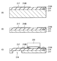
図7は、比較例に係る従来のモジュール100の断面構成を表したものである。このモジュール内のインターポーザ100Aは凹部119を有する第1Si基板(インターポーザ)111上に、下面に配線216およびアンテナ217を有し半導体チップ(集積回路チップ)220を搭載した第2Si基板211が接合金属によって接合されている。なお、凹部119は半導体チップ220を収容するためのものである。
FIG. 7 illustrates a cross-sectional configuration of a
このようなモジュール100を実際に得るためには、図8(A)〜(C),図9(A)〜(C)および図10(A),(B)に示した製造工程が考えられる。各工程を簡単に説明すると、まず、図8(A)に示したように第1Si基板111を加工して貫通孔111Bを形成したのち絶縁膜(図示なし)を形成する。次に図8(B)に示したように貫通電極112Aを形成したのち、パッド113A,113B,113C,113Dを形成する。続いて図8(C)に示したように凹部119を形成し、インターポーザとなる第1Si基板111を作製する。次に図9(A)に示したように第2Si基板211上に配線216A,216Bおよびアンテナ217を備えた誘電体層214を形成したのち、図9(B)に示したように第2Si基板211をCMPにより薄膜化する。続いて、図9(C)に示したように第2Si基板211に凹部219を設けてメンブレン構造としたのち、半導体チップ220を接続し、半導体チップ220を搭載した第2Si基板211を作製する。次に図10(A)に示したように熱圧着により第1Si基板111および第2Si基板211を接合してしたのち、最後に図10(B)に示したように半田を用いてプリント基板130に実装してモジュール100が完成する。
In order to actually obtain such a
このようにして得られたモジュール100およびその製造工程には以下のような問題がある。まず、Si基板を2枚用いるため必然的に大型化する。そのため、これを補う薄膜化工程(図9(B))が必要となる。また、第1Si基板111への凹部119の形成に加えてアンテナ217からの電波放射のために、第2Si基板211の対向する位置に凹部219を設ける必要がある。この際、第2Si基板211は上述のように薄膜化しているため、壊れやすい虞もある。更に、第1Si基板111に第2Si基板211を実装する際には、第1Si基板111の貫通電極112A,112Bおよび第2Si基板211の下面に設けられた配線層216の接合を行う。接合工程は、アライメント精度が低いため微細化の制約となると共に、伝送周波数が高い場合には配線の不整合等による信号損失が顕在化する。また、第1Si基板111および第2Si基板211の接合用の配線加工も必要となる。以上のように製造工程が繁雑となる。
The
これに対して、本実施の形態のインターポーザ10A(10B)では、基板11上に直接形成した誘電体層14中に配線層16を設けることにより、上記工程が不要となるため製造工程の簡略化を図ることが可能となる。
On the other hand, in the
以上のように、本実施の形態のインターポーザ10A(10B)およびこれを備えたモジュール1A(1B)では基板11上に誘電体層14を形成し、この誘電体層14中に配線層16およびアンテナ17を設けるようにした。このように、基板11と配線層16を一体化した構造とすることにより製造工程が簡略化され、歩留まりを向上させることが可能となる。
As described above, in the
また、アライメント精度の低下の原因となる接合工程が削減されるため、モジュール1A(1B)の特性が向上する。更に、製造工程が短縮されるためコストを抑えることもできる。 In addition, since the bonding process that causes a decrease in alignment accuracy is reduced, the characteristics of the module 1A (1B) are improved. Furthermore, since the manufacturing process is shortened, the cost can be suppressed.
また、半導体チップ20とプリント基板30を貫通電極12によって接続するようにしたので、配線面積を縮小することができる。即ち、モジュール1A(1B)の小型化が可能となる。更に、貫通電極12を用いることによってモジュール1A(1B)上に他のモジュールを積層することも可能となる。
Further, since the
また、本実施の形態のインターポーザ10A(10B)およびこれを備えたモジュール1A(1B)では、アンテナ17の少なくとも一部に対応する位置の基板11の裏面側に凹部19A(または基板11を貫通する開口19B)を設けるようにした。これにより基板部分と素子との間での寄生容量や渦電流の発生が抑えられるため、信号損失を抑制することが可能となる。
Further, in the
(変形例)
次に、上記実施の形態のインターポーザ10A(10B)およびこれを備えたモジュール1A(1B)の変形例に係るインターポーザ10C(10D)およびこれを備えたモジュール2A(2B)について説明する。図11は基板11に凹部19Aを有するインターポーザ10Cを備えたモジュール2Aの断面構成を表すものであり、図12はその平面構成を表すものである。図13は基板11に開口19Bを有するインターポーザ10Dを備えたモジュール2Bの断面構成を表すものである。なお、図11および図13は図12のII−II線における断面構造である。上記実施の形態と同一の構成要素については同一符号を付してその説明は省略する。
(Modification)
Next, an interposer 10C (10D) according to a modification of the
このインターポーザ10C(10D)は、配線層16とプリント基板30とをワイヤ33を介して接続したものである。基板11上には、上記実施の形態で説明した配線層16および電気素子17が形成された誘電体層14に加えて、プリント基板30とワイヤ接続するためのワイヤパッドと配線ノイズを除去するためのデカップリングコンデンサ(MIMキャパシタ)(図示せず)と共に、チップ用接続部23が設けられている。
This
本変形例のインターポーザ10C(10D)およびこれを備えたモジュール2A(2B)では、配線層16とプリント基板30とをワイヤ33で接続するようにしたので、上記実施の形態の効果に加えてプリント基板30上にモジュール2A(2B)を自由に配置することが可能となるという効果がある。また、例えばピン数が少なくBGA(Ball Grid Array)等と比較して素子の専有面積の差が小さい場合には、貫通電極12を製造することよりもワイヤ33による配線のほうが安価であるため、コストを低減できるという効果もある。
In the interposer 10C (10D) and the module 2A (2B) having the same in the present modification, the
(適用例)
次に、図14を参照して、本発明のインターポーザ10Aを用いた通信装置の構成について説明する。図14は、電子機器としての通信装置のブロック構成を表している。
(Application example)
Next, a configuration of a communication apparatus using the
図14に示した通信装置は例えば、携帯電話器、情報携帯端末(PDA)、無線LAN機器などである。この通信装置は、例えば、図14に示したように、送信系回路300A(モジュール)と、受信系回路300B(モジュール)と、送受信経路を切り替える送受信切換器301と、高周波フィルタ302と、送受信用のアンテナ303とを備えている。
The communication device shown in FIG. 14 is, for example, a mobile phone, a personal digital assistant (PDA), a wireless LAN device, or the like. For example, as shown in FIG. 14, the communication apparatus includes a
送信系回路300Aは、Iチャンネルの送信データおよびQチャンネルの送信データに対応した2つのデジタル/アナログ変換器(DAC;Digital/Analogue Converter)311I,311Qおよび2つのバンドパスフィルタ312I,312Qと、変調器320および送信用PLL(Phase-Locked Loop)回路313と、電力増幅器314とを備えている。この変調器320は、上記した2つのバンドパスフィルタ312I,312Qに対応した2つのバッファアンプ321I,321Qおよび2つのミキサ322I,322Qと、移相器323と、加算器324と、バッファアンプ325とを含んで構成されている。
The
受信系回路300Bは、高周波部330、バンドパスフィルタ341およびチャンネル選択用PLL回路342と、中間周波回路350およびバンドパスフィルタ343と、復調器360および中間周波用PLL回路344と、Iチャンネルの受信データおよびQチャンネルの受信データに対応した2つのバンドパスフィルタ345I,345Qおよび2つのアナログ/デジタル変換器(ADC;Analogue/Digital Converter)346I,346Qとを備えている。高周波部330は、低ノイズアンプ331と、バッファアンプ332,334と、ミキサ333とを含んで構成されており、中間周波回路350は、バッファアンプ351,353と、自動ゲイン調整(AGC;Auto Gain Controller)回路352とを含んで構成されている。復調器360は、バッファアンプ361と、上記した2つのバンドパスフィルタ345I,345Qに対応した2つのミキサ362I,362Qおよび2つのバッファアンプ363I,363Qと、移相器364とを含んで構成されている。
The reception system circuit 300B includes a
この通信装置では、送信系回路300AにIチャンネルの送信データおよびQチャンネルの送信データが入力されると、それぞれの送信データを以下の手順で処理する。すなわち、まず、DAC311I、311Qにおいてアナログ信号に変換し、引き続きバンドパスフィルタ312I,312Qにおいて送信信号の帯域以外の信号成分を除去したのち、変調器320に供給する。続いて、変調器320において、バッファアンプ321I,321Qを介してミキサ322I,322Qに供給し、引き続き送信用PLL回路313から供給される送信周波数に対応した周波数信号を混合して変調したのち、両混合信号を加算器324において加算することにより1系統の送信信号とする。この際、ミキサ322Iに供給する周波数信号に関しては、移相器323において信号移相を90°シフトさせることにより、Iチャンネルの信号とQチャンネルの信号とが互いに直交変調されるようにする。最後に、バッファアンプ325を介して電力増幅器314に供給することにより、所定の送信電力となるように増幅する。この電力増幅器314において増幅された信号は、送受信切換器301および高周波フィルタ302を介してアンテナ303に供給されることにより、そのアンテナ303を介して無線送信される。この高周波フィルタ302は、通信装置において送信または受信する信号のうちの周波数帯域以外の信号成分を除去するバンドパスフィルタとして機能する。
In this communication apparatus, when I-channel transmission data and Q-channel transmission data are input to the
一方、アンテナ303から高周波フィルタ302および送受信切換器301を介して受信系回路300Bに信号が受信されると、その信号を以下の手順で処理する。すなわち、まず、高周波部330において、受信信号を低ノイズアンプ331で増幅し、引き続きバンドパスフィルタ341で受信周波数帯域以外の信号成分を除去したのち、バッファアンプ332を介してミキサ333に供給する。続いて、チャンネル選択用PPL回路342から供給される周波数信号を混合し、所定の送信チャンネルの信号を中間周波信号とすることにより、バッファアンプ334を介して中間周波回路350に供給する。続いて、中間周波回路350において、バッファアンプ351を介してバンドパスフィルタ343に供給することにより中間周波信号の帯域以外の信号成分を除去し、引き続きAGC回路352でほぼ一定のゲイン信号としたのち、バッファアンプ353を介して復調器360に供給する。続いて、復調器360において、バッファアンプ361を介してミキサ362I,362Qに供給したのち、中間周波用PPL回路344から供給される周波数信号を混合し、Iチャンネルの信号成分とQチャンネルの信号成分とを復調する。この際、ミキサ362Iに供給する周波数信号に関しては、移相器364において信号移相を90°シフトさせることにより、互いに直交変調されたIチャンネルの信号成分とQチャンネルの信号成分とを復調する。最後に、Iチャンネルの信号およびQチャンネルの信号をそれぞれバンドパスフィルタ345I,345Qに供給することによりIチャンネルの信号およびQチャンネルの信号以外の信号成分を除去したのち、ADC346I,346Qに供給してデジタルデータとする。これにより、Iチャンネルの受信データおよびQチャンネルの受信データが得られる。
On the other hand, when a signal is received from the
この通信装置は、上記実施の形態および変形例において説明したインターポーザ10A〜10Dを、アンテナ303、高周波フィルタ302、バンドパスフィルタ341,343、変調器320および復調器360と実装基板との接続に適用しているため、上記実施の形態において説明した作用により、優れた高周波特性を有する。
In this communication apparatus, the
なお、図14に示した通信装置では、上記実施の形態および変形例において説明したインターポーザ10A〜10Dを上記各素子と実装基板との接続に適用する場合について説明したが、必ずしもこれに限られるものではない。例えば、インターポーザ10A〜10Dを微細化に隔たりのあるCMOS素子とMEMSセンサの集積デバイス内における両者の配線の接続に適用してもよい。この場合においても、上記と同様の効果を得ることができる。また、アナログ回路素子とデジタル回路素子の集積化にも適用することができる。
In the communication apparatus shown in FIG. 14, the case where the
以上、実施の形態および変形例を挙げて本発明を説明したが、本発明は上記実施の形態等に限定されるものではなく、種々変形可能である。例えば、上記実施の形態では半導体チップ20とプリント基板30との接続に貫通電極12を用いたが、スルーホール配線によって接続しても同様の効果が得られる。
Although the present invention has been described with reference to the embodiment and the modifications, the present invention is not limited to the above-described embodiment and the like, and various modifications can be made. For example, in the above embodiment, the through
また、上記実施の形態等では電気素子(受動素子)としてアンテナ17を用いたがこれに限らず、例えばインダクタまたはカプラを用いてもよい。更に、受動素子以外の電気素子、例えば高周波スイッチ、高周波伝送線路のカップリングコンデンサとして用いられる場合のバリキャップまたは電気素子を組み合わせたフィルタおよび可変フィルタでもよい。
In the above-described embodiment and the like, the
1A,1B,2A,2B,100…モジュール、10A,10B,10C,10D,100A…インターポーザ、11…基板、11A…絶縁層、12…貫通電極、13A,13B,13C,16C,16D,21A,21B,31A,31B…パッド、14(14A,14B,14C)…誘電体層、15A,15B,15C…ビアコンタクト、16A,16B…配線、16(15A,16A,16B)…配線層、17…アンテナ、18A,18B,19A…凹部、19B…開口、20…半導体チップ、22,32A,32B…半田、30…プリント基板。 1A, 1B, 2A, 2B, 100 ... module, 10A, 10B, 10C, 10D, 100A ... interposer, 11 ... substrate, 11A ... insulating layer, 12 ... penetrating electrode, 13A, 13B, 13C, 16C, 16D, 21A, 21B, 31A, 31B ... Pad, 14 (14A, 14B, 14C) ... Dielectric layer, 15A, 15B, 15C ... Via contact, 16A, 16B ... Wiring, 16 (15A, 16A, 16B) ... Wiring layer, 17 ... Antenna, 18A, 18B, 19A ... recess, 19B ... opening, 20 ... semiconductor chip, 22, 32A, 32B ... solder, 30 ... printed circuit board.
Claims (12)
前記基板の表面側に形成され、半導体チップと電気的に接続される配線と、
前記配線と接続された電気素子と、
前記電気素子に対応する位置に前記基板の裏面側から形成されると共に、底部に前記基板の少なくとも一部が柵状または格子状に残存する凹部と
を備えたインターポーザ。 A substrate having a front surface and a back surface;
Wiring formed on the surface side of the substrate and electrically connected to the semiconductor chip;
An electrical element connected to the wiring;
An interposer which is formed from the back side of the substrate at a position corresponding to the electric element, and has a recess at the bottom of which at least a part of the substrate remains in a fence shape or a lattice shape .
前記インターポーザは、
表面および裏面を有し、表面側に前記半導体チップが実装された基板と、
前記基板の表面側に形成され、前記半導体チップと電気的に接続された配線と、
前記配線と接続された電気素子と、
前記電気素子に対応する位置に前記基板の裏面側から形成されると共に、底部に前記基板の少なくとも一部が柵状または格子状に残存する凹部と
を備えたモジュール。 An interposer and a semiconductor chip mounted on the interposer,
The interposer is
A substrate having a front surface and a back surface, and the semiconductor chip mounted on the front surface side;
Wiring formed on the surface side of the substrate and electrically connected to the semiconductor chip;
An electrical element connected to the wiring;
A module which is formed from the back side of the substrate at a position corresponding to the electric element, and has a recess at the bottom of which at least a part of the substrate remains in a fence shape or a lattice shape .
前記インターポーザは、
表面および裏面を有し、表面側に前記半導体チップが実装された基板と、
前記基板の表面側に形成され、前記半導体チップと電気的に接続された配線と、
前記配線と接続された電気素子と、
前記電気素子に対応する位置に前記基板の裏面側から形成されると共に、底部に前記基板の少なくとも一部が柵状または格子状に残存する凹部と
を備えた電子機器。 An interposer, a semiconductor chip mounted on the interposer, and a mounting board electrically connected to the interposer,
The interposer is
A substrate having a front surface and a back surface, and the semiconductor chip mounted on the front surface side;
Wiring formed on the surface side of the substrate and electrically connected to the semiconductor chip;
An electrical element connected to the wiring;
An electronic device that is formed from a back surface side of the substrate at a position corresponding to the electrical element, and has a concave portion in which at least a part of the substrate remains in a fence shape or a lattice shape at a bottom portion.
Priority Applications (5)
| Application Number | Priority Date | Filing Date | Title |
|---|---|---|---|
| JP2010130266A JP5641202B2 (en) | 2010-06-07 | 2010-06-07 | Interposer, module, and electronic device equipped with the same |
| CN201010241077XA CN101996979B (en) | 2009-08-07 | 2010-07-30 | Interposer, module and electronic device including the same |
| US12/847,240 US20110032685A1 (en) | 2009-08-07 | 2010-07-30 | Interposer, module, and electronics device including the same |
| TW99125503A TWI441307B (en) | 2009-08-07 | 2010-07-30 | Interposer, module, and electronics device including the same |
| EP20100008048 EP2284888A3 (en) | 2009-08-07 | 2010-08-02 | Interposer, module and electronics device including the same |
Applications Claiming Priority (1)
| Application Number | Priority Date | Filing Date | Title |
|---|---|---|---|
| JP2010130266A JP5641202B2 (en) | 2010-06-07 | 2010-06-07 | Interposer, module, and electronic device equipped with the same |
Publications (3)
| Publication Number | Publication Date |
|---|---|
| JP2011258654A JP2011258654A (en) | 2011-12-22 |
| JP2011258654A5 JP2011258654A5 (en) | 2013-07-11 |
| JP5641202B2 true JP5641202B2 (en) | 2014-12-17 |
Family
ID=45474558
Family Applications (1)
| Application Number | Title | Priority Date | Filing Date |
|---|---|---|---|
| JP2010130266A Expired - Fee Related JP5641202B2 (en) | 2009-08-07 | 2010-06-07 | Interposer, module, and electronic device equipped with the same |
Country Status (1)
| Country | Link |
|---|---|
| JP (1) | JP5641202B2 (en) |
Cited By (1)
| Publication number | Priority date | Publication date | Assignee | Title |
|---|---|---|---|---|
| JP7092144B2 (en) | 2017-10-11 | 2022-06-28 | 日本ゼオン株式会社 | Method for manufacturing polymer latex |
Families Citing this family (5)
| Publication number | Priority date | Publication date | Assignee | Title |
|---|---|---|---|---|
| US10651150B2 (en) * | 2014-03-10 | 2020-05-12 | Mitsubishi Heavy Industries, Ltd. | Multichip module including surface mounting part embedded therein |
| WO2018057026A1 (en) * | 2016-09-26 | 2018-03-29 | Nair Vijay K | Die with embedded communication cavity |
| JP7367381B2 (en) * | 2019-08-20 | 2023-10-24 | 富士通株式会社 | Package substrates and electronic equipment |
| JPWO2021200406A1 (en) * | 2020-03-31 | 2021-10-07 | ||
| CN116964738A (en) * | 2021-03-11 | 2023-10-27 | 索尼半导体解决方案公司 | Semiconductor device and electronic apparatus |
Family Cites Families (4)
| Publication number | Priority date | Publication date | Assignee | Title |
|---|---|---|---|---|
| JPH02106956A (en) * | 1988-10-17 | 1990-04-19 | Hitachi Ltd | Semiconductor device and manufacture thereof |
| JP2002374028A (en) * | 2001-06-15 | 2002-12-26 | Kyocera Corp | Wiring board |
| JP2004235602A (en) * | 2002-12-06 | 2004-08-19 | Matsushita Electric Ind Co Ltd | High frequency circuit and manufacturing method thereof |
| JP4979213B2 (en) * | 2005-08-31 | 2012-07-18 | オンセミコンダクター・トレーディング・リミテッド | Circuit board, circuit board manufacturing method, and circuit device |
-
2010
- 2010-06-07 JP JP2010130266A patent/JP5641202B2/en not_active Expired - Fee Related
Cited By (1)
| Publication number | Priority date | Publication date | Assignee | Title |
|---|---|---|---|---|
| JP7092144B2 (en) | 2017-10-11 | 2022-06-28 | 日本ゼオン株式会社 | Method for manufacturing polymer latex |
Also Published As
| Publication number | Publication date |
|---|---|
| JP2011258654A (en) | 2011-12-22 |
Similar Documents
| Publication | Publication Date | Title |
|---|---|---|
| TWI441307B (en) | Interposer, module, and electronics device including the same | |
| JP5641202B2 (en) | Interposer, module, and electronic device equipped with the same | |
| KR101007460B1 (en) | Modular board device and high frequency module and method for producing them | |
| US7851918B2 (en) | Three-dimensional package module | |
| US7741162B2 (en) | Method for manufacturing high-frequency module device | |
| US7940143B2 (en) | Vertical transmission line structure that includes bump elements for flip-chip mounting | |
| JP4835238B2 (en) | RESONATOR, RESONATOR MANUFACTURING METHOD, AND COMMUNICATION DEVICE | |
| US6917259B2 (en) | High-frequency module substrate device | |
| WO2003047325A1 (en) | High-frequency circuit block, its manufacturing method, high-frequency module device, and its manufacturing method | |
| JP2006527499A (en) | Package for high frequency electronic equipment | |
| KR20100032909A (en) | Semiconductor die with backside passive device integration | |
| JP2003115557A (en) | High-frequency module substrate device | |
| US10347616B2 (en) | Chip package and manufacturing method thereof | |
| Hoivik et al. | High-efficiency 60 GHz antenna fabricated using low-cost silicon micromachining techniques | |
| US8987851B2 (en) | Radio-frequency device package and method for fabricating the same | |
| JP2010239344A (en) | Radio circuit module | |
| WO2022220000A1 (en) | High-frequency module and communication device | |
| JP2008112776A (en) | Semiconductor device | |
| JP2023148255A (en) | High frequency circuit board and antenna module | |
| WO2022046562A1 (en) | Device, package and/or substrate comprising curved antenna | |
| JP2010154516A (en) | Resin multilayer device and flip chip mounting device | |
| JP2010267729A (en) | Wireless circuit module | |
| JP2012044063A (en) | Semiconductor module, communication module, and surface-mounted component |
Legal Events
| Date | Code | Title | Description |
|---|---|---|---|
| A521 | Request for written amendment filed |
Free format text: JAPANESE INTERMEDIATE CODE: A523 Effective date: 20130529 |
|
| A621 | Written request for application examination |
Free format text: JAPANESE INTERMEDIATE CODE: A621 Effective date: 20130529 |
|
| A977 | Report on retrieval |
Free format text: JAPANESE INTERMEDIATE CODE: A971007 Effective date: 20131122 |
|
| A131 | Notification of reasons for refusal |
Free format text: JAPANESE INTERMEDIATE CODE: A131 Effective date: 20131127 |
|
| A521 | Request for written amendment filed |
Free format text: JAPANESE INTERMEDIATE CODE: A523 Effective date: 20140117 |
|
| A131 | Notification of reasons for refusal |
Free format text: JAPANESE INTERMEDIATE CODE: A131 Effective date: 20140806 |
|
| A521 | Request for written amendment filed |
Free format text: JAPANESE INTERMEDIATE CODE: A523 Effective date: 20140911 |
|
| TRDD | Decision of grant or rejection written | ||
| A01 | Written decision to grant a patent or to grant a registration (utility model) |
Free format text: JAPANESE INTERMEDIATE CODE: A01 Effective date: 20141001 |
|
| A61 | First payment of annual fees (during grant procedure) |
Free format text: JAPANESE INTERMEDIATE CODE: A61 Effective date: 20141014 |
|
| R151 | Written notification of patent or utility model registration |
Ref document number: 5641202 Country of ref document: JP Free format text: JAPANESE INTERMEDIATE CODE: R151 |
|
| R250 | Receipt of annual fees |
Free format text: JAPANESE INTERMEDIATE CODE: R250 |
|
| R250 | Receipt of annual fees |
Free format text: JAPANESE INTERMEDIATE CODE: R250 |
|
| R250 | Receipt of annual fees |
Free format text: JAPANESE INTERMEDIATE CODE: R250 |
|
| R250 | Receipt of annual fees |
Free format text: JAPANESE INTERMEDIATE CODE: R250 |
|
| LAPS | Cancellation because of no payment of annual fees |