EP3100095B1 - Dispositif de traitement d'un rayonnement lumineux/optique, procede et systeme de conception d'un tel dispositif - Google Patents
Dispositif de traitement d'un rayonnement lumineux/optique, procede et systeme de conception d'un tel dispositif Download PDFInfo
- Publication number
- EP3100095B1 EP3100095B1 EP15702649.3A EP15702649A EP3100095B1 EP 3100095 B1 EP3100095 B1 EP 3100095B1 EP 15702649 A EP15702649 A EP 15702649A EP 3100095 B1 EP3100095 B1 EP 3100095B1
- Authority
- EP
- European Patent Office
- Prior art keywords
- radiation
- correction
- optical elements
- cavity
- reflective optical
- Prior art date
- Legal status (The legal status is an assumption and is not a legal conclusion. Google has not performed a legal analysis and makes no representation as to the accuracy of the status listed.)
- Active
Links
- 230000005855 radiation Effects 0.000 title claims description 148
- 230000003287 optical effect Effects 0.000 title claims description 123
- 238000012545 processing Methods 0.000 title claims description 13
- 238000000034 method Methods 0.000 title description 12
- 238000012937 correction Methods 0.000 claims description 23
- 230000005540 biological transmission Effects 0.000 claims description 22
- 230000010363 phase shift Effects 0.000 claims description 5
- 230000001788 irregular Effects 0.000 claims description 3
- ORQBXQOJMQIAOY-UHFFFAOYSA-N nobelium Chemical compound [No] ORQBXQOJMQIAOY-UHFFFAOYSA-N 0.000 description 12
- 238000012986 modification Methods 0.000 description 10
- 230000004048 modification Effects 0.000 description 10
- 238000005259 measurement Methods 0.000 description 8
- 238000005457 optimization Methods 0.000 description 7
- 230000000644 propagated effect Effects 0.000 description 4
- 238000004519 manufacturing process Methods 0.000 description 3
- 238000004088 simulation Methods 0.000 description 3
- 230000015556 catabolic process Effects 0.000 description 2
- 238000006731 degradation reaction Methods 0.000 description 2
- 238000000151 deposition Methods 0.000 description 2
- 238000013461 design Methods 0.000 description 2
- 238000010586 diagram Methods 0.000 description 2
- 230000000694 effects Effects 0.000 description 2
- 238000005530 etching Methods 0.000 description 2
- 239000004973 liquid crystal related substance Substances 0.000 description 2
- 239000011159 matrix material Substances 0.000 description 2
- 239000003607 modifier Substances 0.000 description 2
- 230000010287 polarization Effects 0.000 description 2
- 230000001902 propagating effect Effects 0.000 description 2
- 239000011347 resin Substances 0.000 description 2
- 229920005989 resin Polymers 0.000 description 2
- 238000012512 characterization method Methods 0.000 description 1
- 238000010276 construction Methods 0.000 description 1
- 238000009826 distribution Methods 0.000 description 1
- 239000000463 material Substances 0.000 description 1
- 230000035939 shock Effects 0.000 description 1
- 238000003860 storage Methods 0.000 description 1
- 239000000758 substrate Substances 0.000 description 1
Images

Classifications
-
- G—PHYSICS
- G02—OPTICS
- G02B—OPTICAL ELEMENTS, SYSTEMS OR APPARATUS
- G02B27/00—Optical systems or apparatus not provided for by any of the groups G02B1/00 - G02B26/00, G02B30/00
- G02B27/0025—Optical systems or apparatus not provided for by any of the groups G02B1/00 - G02B26/00, G02B30/00 for optical correction, e.g. distorsion, aberration
- G02B27/0068—Optical systems or apparatus not provided for by any of the groups G02B1/00 - G02B26/00, G02B30/00 for optical correction, e.g. distorsion, aberration having means for controlling the degree of correction, e.g. using phase modulators, movable elements
-
- G—PHYSICS
- G01—MEASURING; TESTING
- G01J—MEASUREMENT OF INTENSITY, VELOCITY, SPECTRAL CONTENT, POLARISATION, PHASE OR PULSE CHARACTERISTICS OF INFRARED, VISIBLE OR ULTRAVIOLET LIGHT; COLORIMETRY; RADIATION PYROMETRY
- G01J1/00—Photometry, e.g. photographic exposure meter
- G01J1/42—Photometry, e.g. photographic exposure meter using electric radiation detectors
- G01J1/4257—Photometry, e.g. photographic exposure meter using electric radiation detectors applied to monitoring the characteristics of a beam, e.g. laser beam, headlamp beam
-
- G—PHYSICS
- G02—OPTICS
- G02B—OPTICAL ELEMENTS, SYSTEMS OR APPARATUS
- G02B17/00—Systems with reflecting surfaces, with or without refracting elements
- G02B17/004—Systems comprising a plurality of reflections between two or more surfaces, e.g. cells, resonators
-
- G—PHYSICS
- G02—OPTICS
- G02B—OPTICAL ELEMENTS, SYSTEMS OR APPARATUS
- G02B26/00—Optical devices or arrangements for the control of light using movable or deformable optical elements
- G02B26/06—Optical devices or arrangements for the control of light using movable or deformable optical elements for controlling the phase of light
-
- G—PHYSICS
- G02—OPTICS
- G02B—OPTICAL ELEMENTS, SYSTEMS OR APPARATUS
- G02B27/00—Optical systems or apparatus not provided for by any of the groups G02B1/00 - G02B26/00, G02B30/00
- G02B27/0087—Phased arrays
Definitions
- the present invention relates to a device for processing light / optical radiation, in particular by a succession of propagations and modifications of the spatial phase of the light radiation. It also relates to a method and a system for the design of such a device.
- the field of the invention is the field of the treatment of optical radiation and in particular the field of the treatment of optical radiation requiring a succession of propagations of the light radiation.
- an optical resonator provided with an arrangement of reflecting surfaces, between which light is reflected multiple times producing standing waves for certain resonant frequencies.
- the light radiation embraces the entire extent of the cavity defined between the reflecting surfaces, and is reflected at a single reflecting location corresponding to the entire extent of the reflecting surfaces.
- the document WO2012 / 085046 A1 describes a system for correcting the effect of a scattering medium on optical radiation having propagated in this diffusing medium, or to arbitrarily transform the spatial properties of optical radiation. It is a light radiation treatment system.
- the system described in this document comprises a plurality of optical means (phase plates or spatial phase modulators), separated from each other, whose phase profile can be individually adjusted during an optimization step, and which allow each to modify the spatial phase of the light radiation which passes through them or which is reflected on them. It is the sequence of these spatial phase modifications of the light radiation separated by propagations which makes it possible to treat light radiation in general.
- optical means phase plates or spatial phase modulators
- the optical systems provided for processing light radiation comprise a plurality of optical means separated from one another and each performing a given treatment on the optical radiation.
- optical systems which include several optical means making it possible to modify the phase profile of the radiation and in which the optical radiation carries out a succession of propagations have a major drawback.
- the positioning of the optical means with respect to each other and with respect to the light radiation must be very precise, typically of the order of a micron, which can be difficult to achieve, consuming assembly time, and increases the stresses on the rigidity of the assembly.
- the bad positioning of an optical element causes a degradation of the treatment carried out on the optical radiation.
- the optical radiation at the output of the processing device is therefore degraded. This degradation can take the form, for example, of a loss of intensity or an unwanted spatial distortion of the output radiation.
- the object of the invention is to overcome the aforementioned drawbacks.
- Another object of the invention is to provide a device for processing optical radiation that is easier to construct.
- Yet another object of the present invention is to provide a device for processing optical radiation which is faster to construct.
- Another aim of the present invention is to provide a device for processing optical radiation that is more resistant to shocks and vibrations.
- the invention makes it possible to achieve at least one of the aforementioned aims by a device according to claim 1.
- a corrective location changes the phases of at least two spatial components of light radiation differently.
- the device according to the invention processes light or optical radiation through a fixed multipass cavity defined by a small number of optical elements, in which the light radiation is reflected a plurality of times.
- the spatial phase of the light radiation is modified during at least one reflection or transmission on at least one correcting element.
- the device according to the invention produces with the same fixed correcting element, one or more modifications of the spatial phase of the light radiation.
- the device according to the invention makes it possible to carry out a plurality of modifications of the spatial phase of the light radiation with one and the same fixed optical element, which may have different phase profiles for different reflection or transmission locations, whereas the systems of the state of the art provide for using as many optical elements as there are modifications of the spatial phase of the light radiation.
- the device according to the invention is easier to set up, to use and faster to configure, since the number of optical elements to be positioned between them and with respect to the optical radiation is lower.
- the small number of optical elements makes the device according to the invention less expensive to manufacture and makes it possible to improve the rigidity and solidity of the final system.
- the optical radiation is reflected on each reflecting element in turn.
- two reflections of the optical radiation on one of the reflecting optical elements defining the multi-pass cavity are separated by a reflection on the other of the reflecting optical elements defining the multi-pass cavity.
- the spatial phase of the radiation is defined by the phases of all the spatial components of the radiation.
- the “spatial phase profile of a corrective location” (of reflection or transmission) is defined by the set of spatial phase shifts (modifications of the spatial phase) provided by all of the points of reflection or transmission. of said corrective location on the different spatial components of the light radiation during the same reflection or transmission of the radiation on said corrective location.
- the phase profile can be very simple in the case of a reflection on a plane mirror.
- a corrective location can produce either a reflection of the radiation or a transmission of the radiation.
- Each reflecting optical element (of the at least two reflecting optical elements defining a multipass cavity) reflects said light radiation at least four times at different reflection locations.
- the irregularities of a corrective location may exhibit spatial structures at least 5 times smaller than the total size of the corrective location.
- At least one corrective optical element can be formed by one of the reflecting optical elements defining the multipass cavity.
- the number of optical elements of the device according to the invention is reduced because one and the same optical element is both corrective and defines the multipass cavity.
- the device according to the invention can comprise a single correcting element corresponding to one of the reflective optical elements defining the multipass cavity.
- the device according to the invention is simpler to configure and less expensive because it requires a single optical element modifying the spatial phase of the radiation which also defines the multipass cavity.
- the device according to the invention can comprise two correcting elements corresponding respectively to the reflecting optical elements defining the multipass cavity.
- each reflecting optical element defining the multipass cavity comprises at least one corrective reflection location modifying the spatial phase of the radiation.
- the device according to the invention makes it possible to modify the spatial phase of the light radiation by the two reflecting elements defining the multipass cavity. Thus, it is possible to carry out a more complete treatment of the light radiation with a lower number of reflections in the multipass cavity. Consequently, in this version, the device according to the invention carries out a treatment of the light radiation while minimizing the number of optical elements required.
- At least one correcting element can be arranged in the multi-pass cavity and be distinct from the reflecting optical elements defining said multi-pass cavity.
- At least one of the reflective optical elements defining the multipass cavity can also be corrective.
- the reflective optical elements defining the multipass cavity may not be corrective.
- each corrective location has an irregular reflection or transmission surface so that the spatial phase profile of each corrective location has a different phase shift for several points of reflection or transmission of said corrective location.
- the device according to the invention makes it possible to modify the spatial phase of the light radiation during several, in particular all the reflections or transmissions, on the corrective element.
- the device according to the invention makes it possible to carry out a more complete and more complex treatment of the light radiation in the multipass cavity.
- At least two correcting locations which can be of the same correcting element have different phase profiles.
- the device makes it possible to modify the spatial phase of the radiation differently during reflections or transmissions on these two corrective locations of the same corrective optical element.
- At least two correcting locations of the same correcting element have identical phase profiles.
- the device makes it possible to modify in an identical manner the spatial phase of the radiation during reflections or transmission on these two corrective locations of the same corrective optical element.
- At least two correcting locations of two different correcting optical elements may have identical or different spatial phase profiles.
- At least one corrective optical element can be a phase plate.
- At least one corrective optical element can be a phase plate having at least two different spatial phase profiles for at least two corrective locations.
- the phase plate covers at least two different correction locations.
- Each part of the phase plate corresponding to a corrective location has a desired spatial phase profile for that corrective location, which may be different from the desired spatial phase profile for another corrective location covered by the phase slide.
- the single phase plate covering several corrective locations comprises at least two parts having different spatial phase profiles.
- the phase plate can be an etched mirror, but can also be a resin deposited on a substrate.
- At least one corrective optical element can be a spatial phase modulator having at least two different spatial phase profiles for at least two corrective locations.
- the spatial phase modulator covers at least two different correction locations.
- Each part of the spatial phase modulator corresponding to a corrective location has a desired spatial phase profile for that corrective location, which may be different from the desired spatial phase profile for another corrective location covered by the phase plate.
- the single spatial phase modulator covering several corrective locations comprises at least two parts having different spatial phase profiles. In this embodiment the cost of the device according to the invention is reduced because a single spatial phase modulator is necessary for the device.
- the spatial phase modulator can be a mirror deformed by actuators, but can also be a liquid crystal matrix whose birefringence properties are controlled by a matrix of electrodes.
- At least one reflecting element defining the multi-pass cavity can comprise a through opening making it possible to inject the optical radiation to be treated into the multi-pass cavity and / or to exit the optical radiation from said multi-pass cavity after treatment.
- one of the reflecting optical elements may have a flat reflecting surface.
- one of the reflecting optical elements has a curved reflecting surface.
- planar surface may be a phase plate having one or more corrective reflection locations, the curved surface applying no modification of the particular spatial phase of the light radiation other than the mentioned curvature.
- the reflective optical elements defining the multipass cavity can be positioned in two directions perpendicular to each other.
- the device according to the invention may further comprise a mirror, called an intermediate mirror, arranged opposite said reflecting optical elements at an angle of 45 ° with respect to the direction of each of said reflecting optical elements, and reflecting 99% of the light. light radiation.
- the intermediate mirror may or may not be a correcting element.
- the device according to the invention is easier to configure because it is easy to observe each of the optical elements. individually reflecting by observing, for example, the 1% of the light radiation which passes through the intermediate mirror.
- the multipass cavity is called “angled”.
- the method may include a step for collecting data on the geometry of the multi-pass cavity by measuring the positions and the amplitude distribution of the reflections or transmissions of the reference radiation and / or to be treated, on the various optical elements in the absence of a phase profile.
- a measurement can be carried out by a measurement means, such as a CCD camera, placed opposite or behind the location of reflection or transmission.
- the intermediate mirror can be partly reflecting and the measuring means, for example the CCD camera, can be placed behind the intermediate mirror facing the corrective location, and more generally facing of the reflecting or transmitting element on which the corrective reflection location is located.
- the measuring means for example the CCD camera
- the radiation to be treated and / or the reference radiation can be propagated in the multipass cavity by simulation on computer means, the simulation taking into account the characteristics of the cavity, namely optical and physical characteristics of the optical elements defining the cavity, the length of the cavity, the relative angles of different optical elements, etc; characteristics calculated using, among other things, the information captured during the step of collecting data relating to the geometry of the multipass cavity.
- the propagation of the virtual reference radiations and to be treated through the cavity can be carried out to provide the characteristics of the reference radiations and to be treated at the level of each of the corrective locations in the cavity, namely the intensity and the phase shift of each spatial component of the reference radiation and of the radiation to be processed at each of the corrective locations, so as to determine the correlation parameter of these two radiations as described above.
- the radiation to be treated is obtained at the outlet of the scattering medium and the reference radiation can advantageously be identical to said radiation to be treated before said radiation to be treated has passed through said scattering medium.
- the reference radiation can be identical to the radiation to be treated before the latter passes through the scattering medium.
- the correlation parameter can be determined at each corrective, reflection or transmission location in the multipass cavity, or only at a portion of only the corrective locations in the cavity.
- the correlation parameter can be measured only at the corrective locations provided for applying a treatment to the optical radiation to be treated.
- This correlation parameter can be the spatial phase difference between the radiation to be processed and the reference radiation.
- the correlation parameter can be measured at the outlet of the multipass cavity.
- the document WO2012 / 085046 A1 includes more precision on interference measurements and optimization.
- the method of configuring a corrective location can comprise a step of measuring the characteristics of the radiation to be processed and of reference at this correcting location.
- a measurement can be carried out by a measurement means, such as a CCD camera, placed opposite or behind the correcting location.
- the intermediate mirror can be partly reflecting and the measuring means, for example the CCD camera, can be placed behind the intermediate mirror facing the corrective location, and more generally facing of the reflecting / transmitting element on which the corrective location is located.
- the measuring means for example the CCD camera
- the phase plate can be either an individual phase plate for a corrector location, or a phase plate common to several corrector locations and having different phase profiles optimized on different regions of its surface each corresponding to a corrector location.
- the FIGURE 1 is a schematic representation of a first non-limiting example of a device for processing light radiation.
- the device 100 shown in FIGURE 1 comprises two reflecting optical elements 102 and 104 forming between them a multipass cavity 106 in which a light radiation to be treated 108 undergoes a plurality of reflections and propagations.
- the reflective element 104 has a through opening 110 allowing optical radiation to enter the multipass cavity 106 to be processed and to exit the cavity 106 after being processed.
- the reflective element 102 has a flat reflective surface 112 and the reflective element 104 has a concave or curved reflective surface 114.
- the multipass cavity defined by the mirrors 102 and 104 is arranged so that the light radiation 108 is reflected a plurality of times by each of the mirrors, at different locations, and this in turn.
- the plane mirror 102 reflects the radiation optical 108 eight times at eight different reflection locations on the planar surface 112 and the curved mirror 104 reflects optical radiation 108 seven times, at seven different reflection locations on the planar surface 114.
- the reflecting element 104 is formed by a curved or concave mirror and does not apply any modification to the spatial phase profile of the optical radiation 108 outside of its curvature.
- the reflecting element 102 is said to be corrective.
- This reflecting element 102 is formed by a plane mirror, the reflecting surface 112 of which is deformed to the scale of the wavelength, applying a modification of the spatial phase of the optical radiation.
- the deformed plane mirror has, at each reflection location 116, an irregular surface so that each reflection location 116 is corrective and has a spatial phase profile modifying the spatial phase of the radiation 108.
- each region / zone / location of reflection 116 1 -116 8 has different depths for at least two spatial components of the radiation 108 and achieves a modification of the spatial phase of the optical radiation 108, that is to say different phase shifts of at least minus two spatial components of radiation 108.
- Each reflecting optical element 102, 104 is arranged to reflect said light radiation 108 a plurality of times (at least 4 times, preferably at least 6 times).
- the multipass cavity 106 is arranged so that the light radiation 108 makes several round trips between the (at least) two reflective optical elements 102, 104.
- the reflecting element 104 is not corrective.
- the reflecting element 104 can also be corrective, at least for part of the reflection locations on this reflecting element 104.
- the reflecting element 102 is corrective for each reflection location on this reflecting element 102.
- the reflecting element 102 may be corrector for only part of the reflection locations on this reflecting element 102.
- each corrective reflection location 116 is shown differently, i.e. with different spatial phase profiles.
- each corrective reflection location 116 can have the same irregularity, that is to say a phase profile identical to that of another corrective reflection location 116.
- the FIGURE 2 is a schematic representation of a second non-limiting example of a device for processing light radiation.
- the device 200 shown in FIGURE 2 includes all components of the device 100 of the FIGURE 1 .
- the reflecting elements 102 and 104 are arranged in two directions, 202 and 204 respectively, perpendicular to each other, while on the FIGURE 1 they are arranged in the same direction or in two directions parallel to each other.
- the multipass cavity 106 obtained with the device of the FIGURE 2 is said to be angled.
- the device 200 further comprises an intermediate mirror 206, arranged opposite the reflecting elements at an angle 45 ° with respect to each of the directions 202 and 204.
- the role of the intermediate mirror 206 is to direct the optical radiation 108 coming from a reflective elements 102 or 104 towards the other of the reflective elements 104 or 102.
- the intermediate mirror 206 is a 99% reflective mirror. Consequently, this mirror 206 allows 1% of the radiation 108 to pass each time it is reflected on this intermediate mirror 206.
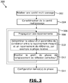
- the FIGURE 3 is a representation in the form of a diagram of a non-limiting example of a method for designing a device according to the invention.
- the method 300 comprises an initial step 302 of producing a multipass cavity, for example the cavity 106 by association of two mirrors 104 and 106.
- the method then comprises a step 304 of characterizing the geometry of the measurement cavity, that is to say the determination of the geometric characteristics of the cavity, of the locations of reflection, etc.
- a step can be carried out by propagation in the cavity of radiation, for example radiation to be treated.
- Steps 308-312 are iterated as many times as necessary to obtain an optimized coverage value (spatial scalar product) of the radiation, for example determined beforehand.
- step 314 carried out after step 306, one or more phase plates, comprising for each correcting reflection location the optimized phase profile, are printed on the reflecting element concerned, for example by etching the face. reflective 112 of mirror 102.
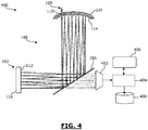
- the FIGURE 4 is a schematic representation of a non-limiting example of a system for designing a device according to the invention.
- the system 400 comprises a CCD camera 402 making it possible to measure the radiation to be treated at the level of a plurality of reflection locations on a reflecting element defining the multi-pass cavity, these measurements making it possible both to characterize the radiation to be treated as well as the geometric properties of the multipass cavity.
- a module 404 makes it possible, by simulation, to apply different phase profiles for each of the correcting reflection locations concerned with a view to determining the phase profile optimized for each correcting reflection location.
- the phase profile at the location considered in the module 404 is modified.
- the phase profiles determined by the module 404 providing this optimized value are stored in storage means 408.
- phase plates are then used to fabricate / configure one or more phase plates, intended to be placed in place of the reflecting element concerned.
- the system 400 is shown in combination with the device 200 of the FIGURE 2 .
- the CCD camera 402 is positioned behind the intermediate mirror 206 and is focused on the reflecting surface of the reflecting element concerned, namely the reflecting surface 112 of the plane mirror 102.
- the system 400 of the FIGURE 4 it is also possible to use the system 400 of the FIGURE 4 to design a device according to the configuration shown in FIGURE 1 .
- the CCD camera 402 is positioned behind the reflecting element concerned, namely behind the mirror 102.
- the correcting element is an optical element defining the multipass cavity.
- the corrective optical element which is distinct from the reflecting optical elements defining the cavity. multipass and disposed between these reflecting elements, such a correcting optical element possibly being an optical element reflecting or transmitting optical radiation, such as for example the intermediate mirror 206 of the FIGURE 2 .
- the corrective locations are all locations reflecting light radiation.
Landscapes
- Physics & Mathematics (AREA)
- Optics & Photonics (AREA)
- General Physics & Mathematics (AREA)
- Spectroscopy & Molecular Physics (AREA)
- Optical Elements Other Than Lenses (AREA)
- Lenses (AREA)
- Mechanical Light Control Or Optical Switches (AREA)
- Exposure Of Semiconductors, Excluding Electron Or Ion Beam Exposure (AREA)
Applications Claiming Priority (2)
| Application Number | Priority Date | Filing Date | Title |
|---|---|---|---|
| FR1450715A FR3016973B1 (fr) | 2014-01-30 | 2014-01-30 | Dispositif de traitement d'un rayonnement lumineux/optique, procede et systeme de conception d'un tel dispositif |
| PCT/EP2015/050711 WO2015113831A1 (fr) | 2014-01-30 | 2015-01-15 | Dispositif de traitement d'un rayonnement lumineux/optique, procede et systeme de conception d'un tel dispositif |
Publications (2)
| Publication Number | Publication Date |
|---|---|
| EP3100095A1 EP3100095A1 (fr) | 2016-12-07 |
| EP3100095B1 true EP3100095B1 (fr) | 2021-03-10 |
Family
ID=51063533
Family Applications (1)
| Application Number | Title | Priority Date | Filing Date |
|---|---|---|---|
| EP15702649.3A Active EP3100095B1 (fr) | 2014-01-30 | 2015-01-15 | Dispositif de traitement d'un rayonnement lumineux/optique, procede et systeme de conception d'un tel dispositif |
Country Status (8)
Families Citing this family (29)
| Publication number | Priority date | Publication date | Assignee | Title |
|---|---|---|---|---|
| FR3049135B1 (fr) | 2016-03-15 | 2020-02-14 | Cailabs | Dispositf de communications par fibre optique multimode avec composant de compensation de dispersion modale |
| FR3049134B1 (fr) * | 2016-03-15 | 2018-07-13 | Cailabs | Dispositf de communications par fibre optique multimode avec interversion de modes de propagation |
| FR3061964A1 (fr) | 2017-01-19 | 2018-07-20 | Cailabs | Transformation de la variation d'un parametre d'un faisceau en la variation d'un autre de ses parametres |
| FR3076358B1 (fr) | 2017-12-28 | 2019-12-20 | Cailabs | Dispositif optique disposant de moyens pour son assemblage precis, procede d'assemblage ou de test de ce dispositif |
| FR3076357B1 (fr) | 2017-12-29 | 2021-10-22 | Cailabs | Cavite multi passage d’un dispositif optique de manipulation spatiale d’un rayonnement lumineux. |
| FR3076356B1 (fr) * | 2017-12-29 | 2020-01-31 | Cailabs | Cavité monolithique pour la manipulation de la lumière |
| FR3077889B1 (fr) | 2018-02-12 | 2023-03-03 | Cailabs | Dispositif optique de compensation des imperfections des composants optiques composant le dispositif et procede de fabrication d'un tel dispositif |
| FR3078412B1 (fr) | 2018-02-26 | 2022-01-14 | Cailabs | Procede de conception d’un dispositif de conversion multiplan, lame de phase obtenus par l’intermediaire de ce procede, et dispositif de conversion multiplan |
| FR3084478A3 (fr) | 2018-07-25 | 2020-01-31 | Cailabs | Dispositif de filtrage modal comprenant un dispositif de conversion de lumiere multiplan |
| WO2020021196A1 (fr) | 2018-07-25 | 2020-01-30 | Cailabs | Dispositif de traitement d'un rayonnement lumineux comprenant un dispositif de conversion de lumiere multiplan |
| FR3092404B1 (fr) | 2019-02-04 | 2021-10-22 | Cailabs | Dispositif optique de combinaison d'une pluralite de faisceaux, et systeme employant un tel dispositif |
| FR3097334A1 (fr) | 2019-06-17 | 2020-12-18 | Cailabs | Procédé de fixation d’une fibre optique monomode et d’une fibre optique multimode, equipement de couplage optique et fibre optique pouvant être obtenue grace à un tel procédé |
| FR3097659B1 (fr) | 2019-06-21 | 2024-04-19 | Cailabs | Source lumineuse comportant au moins une puce à semi-conducteur portant au moins une diode |
| US12007579B2 (en) | 2019-10-30 | 2024-06-11 | Nec Corporation | Machine learning based regression of complex coefficients of a linear combination of spatial modes from multimode optical fiber |
| FR3104271B1 (fr) | 2019-12-04 | 2021-12-17 | Alpao | Systeme d’optique adaptative a temps de reponse ameliore, utilisation et procede afferents |
| FR3106668B1 (fr) | 2020-01-29 | 2022-01-21 | Cailabs | Dispositif de traitement d’un faisceau lumineux par l'intermediaire d’un convertisseur multi plan pour le conformer à une forme prédéterminée |
| FR3106889B1 (fr) | 2020-01-30 | 2022-02-25 | Safran | Système de mesure d’une pluralité de paramètres physiques en un point de mesure par une fibre optique multimode |
| WO2021155302A1 (en) | 2020-01-31 | 2021-08-05 | Corning Incorporated | Wavelength multiplexer/demultiplexer using metamaterials for optical fiber communications |
| EP4097522A1 (en) | 2020-01-31 | 2022-12-07 | Corning Incorporated | Mode multiplexer/demultiplexer using metamaterials for optical communication system, and optical communication |
| FR3120450B1 (fr) | 2021-03-04 | 2023-11-24 | Cailabs | Système de compensation de la distorsion d’un front d’onde d’un rayonnement lumineux incident |
| FR3128798B1 (fr) | 2021-10-28 | 2025-01-17 | Cailabs | Dispositif de traitement d’au moins deux Faisceaux lumineux monomodes |
| US11940686B2 (en) * | 2022-04-12 | 2024-03-26 | Ii-Vi Delaware, Inc. | Spatial light modulator incorporating aberration correction |
| FR3137189B1 (fr) | 2022-06-27 | 2025-03-14 | Cailabs | Cavite multi passage d’un dispositif optique de manipulation spatiale d’un rayonnement lumineux |
| FR3142310A1 (fr) | 2022-11-21 | 2024-05-24 | Cailabs | Système de telecommunication optique en espace libre |
| FR3144459A1 (fr) | 2022-12-22 | 2024-06-28 | Thales | Circuit photonique intégré de démultiplexage d'un faisceau optique incident fortement multimode et de recombinaison |
| FR3147876A1 (fr) | 2023-04-14 | 2024-10-18 | Cailabs | Système photonique comprenant une puce photonique et un dispositif de conversion multiplan |
| FR3148885A1 (fr) | 2023-05-19 | 2024-11-22 | Cailabs | Dispositif de traitement optique d’un rayonnement lumineux incident s’etant propage en espace libre |
| FR3148886A1 (fr) | 2023-05-19 | 2024-11-22 | Cailabs | Systeme de telecommunication optique en espace libre |
| FR3154512A1 (fr) | 2023-10-24 | 2025-04-25 | Cailabs | Dispositif optique de combinaison cohérente et Système employant un tel dispositif pour éclairer une cible en champ lointain |
Citations (5)
| Publication number | Priority date | Publication date | Assignee | Title |
|---|---|---|---|---|
| US5058123A (en) * | 1986-12-08 | 1991-10-15 | Mitsubishi Denki K.K. | Laser apparatus |
| US5586139A (en) * | 1992-10-21 | 1996-12-17 | Mitsubishi Denki Kabushiki Kaisha | Laser system |
| US5946330A (en) * | 1994-11-30 | 1999-08-31 | Daimler-Benz Ag | Multiple path resonator with longitudinal pump arrangement |
| EP0979546A1 (en) * | 1997-05-01 | 2000-02-16 | Yeda Research And Development Co. Ltd. | Optical resonators with discontinuous phase elements |
| US6134259A (en) * | 1996-03-14 | 2000-10-17 | Yeda Research And Development Co., Ltd. | Optical resonator with spiral optical elements |
Family Cites Families (22)
| Publication number | Priority date | Publication date | Assignee | Title |
|---|---|---|---|---|
| US4393303A (en) * | 1981-05-04 | 1983-07-12 | United Technologies Corporation | Intracavity phase front and power control |
| JPS57190382A (en) | 1981-05-19 | 1982-11-22 | Sumitomo Electric Ind Ltd | Laser oscillator |
| JPS6464278A (en) | 1987-09-03 | 1989-03-10 | Mitsubishi Electric Corp | Laser equipment |
| JPH01194375A (ja) | 1988-01-29 | 1989-08-04 | Toshiba Corp | レーザパルスストレッチャー |
| US5033060A (en) * | 1990-05-22 | 1991-07-16 | Massachusetts Institute Technology | Optical device for laser coupling and coherent beam combining |
| JPH0821964A (ja) | 1994-07-05 | 1996-01-23 | Hitachi Ltd | 形状可変鏡の制御法及び補償光学装置 |
| JPH1194375A (ja) * | 1997-09-24 | 1999-04-09 | Mitsubishi Heavy Ind Ltd | 空気調和機 |
| JP2000091681A (ja) * | 1998-09-09 | 2000-03-31 | Japan Atom Energy Res Inst | 波面制御をすることにより媒質中にレーザー光を長距離伝播させる方法 |
| JP2000174365A (ja) | 1998-12-02 | 2000-06-23 | Amada Eng Center Co Ltd | レーザ発振器 |
| US6430328B1 (en) * | 2000-10-13 | 2002-08-06 | William H. Culver | Optical switch |
| WO2003020121A1 (en) * | 2001-08-30 | 2003-03-13 | University Of Rochester | Adaptive optics in a scanning lase ophtalmoscope |
| DE10203864A1 (de) * | 2002-01-28 | 2003-08-07 | Univ Schiller Jena | Verfahren zur Amplituden- und/oder Phasenmodulation breitbandiger Laserimpulse sowie Vorrichtung zur Durchführung des Verfahrens |
| US7590156B1 (en) * | 2004-05-17 | 2009-09-15 | University Of Central Florida Research Foundation, Inc. | High intensity MHz mode-locked laser |
| JP4254654B2 (ja) | 2004-08-17 | 2009-04-15 | 株式会社島津製作所 | レーザ式多重反射セル式ガス分析計 |
| US8102593B2 (en) * | 2007-08-07 | 2012-01-24 | Onyx Optics, Inc. | Quasi non-critical phase matched and contra-phase matched structures |
| JP2010040784A (ja) | 2008-08-05 | 2010-02-18 | Fanuc Ltd | レーザ加工装置 |
| CN101521351A (zh) | 2009-03-25 | 2009-09-02 | 中国科学院上海光学精密机械研究所 | 光束扫描激光器 |
| CN201518383U (zh) * | 2009-09-28 | 2010-06-30 | 深圳大学 | 一种中红外相干光源装置 |
| EP2469221A1 (en) * | 2010-12-21 | 2012-06-27 | Universite Pierre Et Marie Curie - Paris 6 | Method and system for configuring a device for correcting the effect of a medium on a light signal, method, device and system for correcting said effect. |
| DE102011008225B3 (de) | 2011-01-10 | 2012-02-23 | Fraunhofer-Gesellschaft zur Förderung der angewandten Forschung e.V. | Optischer Resonator mit direktem geometrischem Zugang auf der optischen Achse |
| US8531659B2 (en) | 2011-03-24 | 2013-09-10 | The Laser Sensing Company | Multipass cell using spherical mirrors while achieving dense spot patterns |
| CN102280809B (zh) | 2011-07-14 | 2014-07-30 | 苏州多谱激光科技有限公司 | 外腔式电光可调激光器 |
-
2014
- 2014-01-30 FR FR1450715A patent/FR3016973B1/fr not_active Expired - Fee Related
-
2015
- 2015-01-15 AU AU2015213086A patent/AU2015213086A1/en not_active Abandoned
- 2015-01-15 EP EP15702649.3A patent/EP3100095B1/fr active Active
- 2015-01-15 CA CA2936562A patent/CA2936562C/fr active Active
- 2015-01-15 CN CN201580006509.XA patent/CN106030372B/zh active Active
- 2015-01-15 JP JP2016567142A patent/JP6561072B2/ja active Active
- 2015-01-15 WO PCT/EP2015/050711 patent/WO2015113831A1/fr active Application Filing
- 2015-01-15 CN CN201910897652.2A patent/CN110764240B/zh active Active
- 2015-01-15 US US15/113,761 patent/US10324286B2/en active Active
-
2019
- 2019-05-07 US US16/405,645 patent/US10627619B2/en active Active
Patent Citations (5)
| Publication number | Priority date | Publication date | Assignee | Title |
|---|---|---|---|---|
| US5058123A (en) * | 1986-12-08 | 1991-10-15 | Mitsubishi Denki K.K. | Laser apparatus |
| US5586139A (en) * | 1992-10-21 | 1996-12-17 | Mitsubishi Denki Kabushiki Kaisha | Laser system |
| US5946330A (en) * | 1994-11-30 | 1999-08-31 | Daimler-Benz Ag | Multiple path resonator with longitudinal pump arrangement |
| US6134259A (en) * | 1996-03-14 | 2000-10-17 | Yeda Research And Development Co., Ltd. | Optical resonator with spiral optical elements |
| EP0979546A1 (en) * | 1997-05-01 | 2000-02-16 | Yeda Research And Development Co. Ltd. | Optical resonators with discontinuous phase elements |
Also Published As
| Publication number | Publication date |
|---|---|
| CA2936562A1 (fr) | 2015-08-06 |
| US20170010463A1 (en) | 2017-01-12 |
| US20190265464A1 (en) | 2019-08-29 |
| FR3016973A1 (fr) | 2015-07-31 |
| JP2017506770A (ja) | 2017-03-09 |
| CN110764240A (zh) | 2020-02-07 |
| US10627619B2 (en) | 2020-04-21 |
| JP6561072B2 (ja) | 2019-08-14 |
| FR3016973B1 (fr) | 2017-08-11 |
| WO2015113831A1 (fr) | 2015-08-06 |
| CN110764240B (zh) | 2021-06-01 |
| CA2936562C (fr) | 2023-04-04 |
| AU2015213086A1 (en) | 2016-08-11 |
| CN106030372A (zh) | 2016-10-12 |
| EP3100095A1 (fr) | 2016-12-07 |
| US10324286B2 (en) | 2019-06-18 |
| CN106030372B (zh) | 2019-10-11 |
Similar Documents
| Publication | Publication Date | Title |
|---|---|---|
| EP3100095B1 (fr) | Dispositif de traitement d'un rayonnement lumineux/optique, procede et systeme de conception d'un tel dispositif | |
| FR2948775A1 (fr) | Systeme optique planaire d'imagerie polychromatique a large champ de vision | |
| EP3206059A1 (fr) | Composant diffractif sub longueur d'onde large bande spectrale | |
| EP1974194B1 (fr) | Interferometre optique achromatique et compact, du type a decalage trilateral | |
| FR2960291A1 (fr) | Methode et dispositif de microscopie interferentielle plein champ a haute resolution | |
| FR3022346A1 (fr) | Dispositif et procede de caracterisation d'un faisceau de lumiere | |
| EP2572235B1 (fr) | Design et realisation d'un composant optique transparent a structure cellulaire | |
| WO2007093748A2 (fr) | Procede d'analyse de surface d'onde par interferometrie multilaterale a difference de frequence | |
| WO2015181130A1 (fr) | Systeme de mise en phase d'un grand nombre de sources laser | |
| FR3021111A1 (fr) | Pyrometre accordable en longueur d'onde pour la mesure par voie radiometrique de la temperature d'un corps | |
| EP1061349A1 (fr) | Interféromètre optique achromatique, du type à sensibilité continûment réglable | |
| WO2010089511A1 (fr) | Dispositif autocorrelateur a biprisme pour la mesure temporelle d'impulsions de lumiere ultrabreves | |
| EP3345264B1 (fr) | Système de mesure de durée, de profil temporel et de spectre d'impulsion laser ultrabrève | |
| FR2976663A1 (fr) | Dispositif et procede de caracterisation d'un faisceau de lumiere. | |
| WO2016062942A1 (fr) | Procede et système pour la generation d'une puissance laser elevee | |
| EP3615902B1 (fr) | Procede de caracterisation spatio-spectrale d'une source laser impulsionnelle polychromatique | |
| EP2708862B1 (fr) | Instrument d'optique à analyseur de front d'onde | |
| EP3564634A1 (fr) | Procede d'insensibilisation a la defocalisation par masque de phase d'un spectrometre pour instruments d'observation embarques | |
| EP3525015A1 (fr) | Élement optique monobloc a diaphragme | |
| FR3077889A1 (fr) | Dispositif optique de compensation des imperfections des composants optiques composant le dispositif et procede de fabrication d'un tel dispositif | |
| EP3679424B1 (fr) | Système de conversion de fréquence amélioré | |
| WO2017198971A1 (fr) | Installation et procede de mesure d'un etat de surface ou de volume d'un objet par diffusion en champ lointain | |
| FR3059156B1 (fr) | Module de detection optique | |
| FR3038193A1 (fr) | Procede de conception d'un systeme d'imagerie, filtre spatial et systeme d'imagerie comportant un tel filtre spatial | |
| EP3192189A1 (fr) | Dispositif et procede de compensation de dispersion chromatique |
Legal Events
| Date | Code | Title | Description |
|---|---|---|---|
| PUAI | Public reference made under article 153(3) epc to a published international application that has entered the european phase |
Free format text: ORIGINAL CODE: 0009012 |
|
| STAA | Information on the status of an ep patent application or granted ep patent |
Free format text: STATUS: REQUEST FOR EXAMINATION WAS MADE |
|
| 17P | Request for examination filed |
Effective date: 20160721 |
|
| AK | Designated contracting states |
Kind code of ref document: A1 Designated state(s): AL AT BE BG CH CY CZ DE DK EE ES FI FR GB GR HR HU IE IS IT LI LT LU LV MC MK MT NL NO PL PT RO RS SE SI SK SM TR |
|
| AX | Request for extension of the european patent |
Extension state: BA ME |
|
| DAX | Request for extension of the european patent (deleted) | ||
| STAA | Information on the status of an ep patent application or granted ep patent |
Free format text: STATUS: EXAMINATION IS IN PROGRESS |
|
| 17Q | First examination report despatched |
Effective date: 20180314 |
|
| REG | Reference to a national code |
Ref country code: DE Ref legal event code: R079 Ref document number: 602015066607 Country of ref document: DE Free format text: PREVIOUS MAIN CLASS: G02B0026060000 Ipc: G02B0017000000 |
|
| GRAP | Despatch of communication of intention to grant a patent |
Free format text: ORIGINAL CODE: EPIDOSNIGR1 |
|
| STAA | Information on the status of an ep patent application or granted ep patent |
Free format text: STATUS: GRANT OF PATENT IS INTENDED |
|
| RIC1 | Information provided on ipc code assigned before grant |
Ipc: G02B 27/00 20060101ALI20200908BHEP Ipc: G02B 26/06 20060101ALI20200908BHEP Ipc: G01J 1/42 20060101ALI20200908BHEP Ipc: G02B 17/00 20060101AFI20200908BHEP |
|
| INTG | Intention to grant announced |
Effective date: 20201001 |
|
| RIN1 | Information on inventor provided before grant (corrected) |
Inventor name: LABROILLE, GUILLAUME Inventor name: MORIZUR, JEAN-FRANCOIS Inventor name: TREPS, NICOLAS |
|
| GRAS | Grant fee paid |
Free format text: ORIGINAL CODE: EPIDOSNIGR3 |
|
| GRAA | (expected) grant |
Free format text: ORIGINAL CODE: 0009210 |
|
| STAA | Information on the status of an ep patent application or granted ep patent |
Free format text: STATUS: THE PATENT HAS BEEN GRANTED |
|
| AK | Designated contracting states |
Kind code of ref document: B1 Designated state(s): AL AT BE BG CH CY CZ DE DK EE ES FI FR GB GR HR HU IE IS IT LI LT LU LV MC MK MT NL NO PL PT RO RS SE SI SK SM TR |
|
| REG | Reference to a national code |
Ref country code: GB Ref legal event code: FG4D Free format text: NOT ENGLISH |
|
| REG | Reference to a national code |
Ref country code: AT Ref legal event code: REF Ref document number: 1370468 Country of ref document: AT Kind code of ref document: T Effective date: 20210315 Ref country code: CH Ref legal event code: EP |
|
| REG | Reference to a national code |
Ref country code: DE Ref legal event code: R096 Ref document number: 602015066607 Country of ref document: DE |
|
| REG | Reference to a national code |
Ref country code: IE Ref legal event code: FG4D Free format text: LANGUAGE OF EP DOCUMENT: FRENCH |
|
| REG | Reference to a national code |
Ref country code: LT Ref legal event code: MG9D |
|
| PG25 | Lapsed in a contracting state [announced via postgrant information from national office to epo] |
Ref country code: LT Free format text: LAPSE BECAUSE OF FAILURE TO SUBMIT A TRANSLATION OF THE DESCRIPTION OR TO PAY THE FEE WITHIN THE PRESCRIBED TIME-LIMIT Effective date: 20210310 Ref country code: FI Free format text: LAPSE BECAUSE OF FAILURE TO SUBMIT A TRANSLATION OF THE DESCRIPTION OR TO PAY THE FEE WITHIN THE PRESCRIBED TIME-LIMIT Effective date: 20210310 Ref country code: GR Free format text: LAPSE BECAUSE OF FAILURE TO SUBMIT A TRANSLATION OF THE DESCRIPTION OR TO PAY THE FEE WITHIN THE PRESCRIBED TIME-LIMIT Effective date: 20210611 Ref country code: HR Free format text: LAPSE BECAUSE OF FAILURE TO SUBMIT A TRANSLATION OF THE DESCRIPTION OR TO PAY THE FEE WITHIN THE PRESCRIBED TIME-LIMIT Effective date: 20210310 Ref country code: BG Free format text: LAPSE BECAUSE OF FAILURE TO SUBMIT A TRANSLATION OF THE DESCRIPTION OR TO PAY THE FEE WITHIN THE PRESCRIBED TIME-LIMIT Effective date: 20210610 Ref country code: NO Free format text: LAPSE BECAUSE OF FAILURE TO SUBMIT A TRANSLATION OF THE DESCRIPTION OR TO PAY THE FEE WITHIN THE PRESCRIBED TIME-LIMIT Effective date: 20210610 |
|
| REG | Reference to a national code |
Ref country code: AT Ref legal event code: MK05 Ref document number: 1370468 Country of ref document: AT Kind code of ref document: T Effective date: 20210310 |
|
| REG | Reference to a national code |
Ref country code: NL Ref legal event code: MP Effective date: 20210310 |
|
| PG25 | Lapsed in a contracting state [announced via postgrant information from national office to epo] |
Ref country code: SE Free format text: LAPSE BECAUSE OF FAILURE TO SUBMIT A TRANSLATION OF THE DESCRIPTION OR TO PAY THE FEE WITHIN THE PRESCRIBED TIME-LIMIT Effective date: 20210310 Ref country code: LV Free format text: LAPSE BECAUSE OF FAILURE TO SUBMIT A TRANSLATION OF THE DESCRIPTION OR TO PAY THE FEE WITHIN THE PRESCRIBED TIME-LIMIT Effective date: 20210310 Ref country code: RS Free format text: LAPSE BECAUSE OF FAILURE TO SUBMIT A TRANSLATION OF THE DESCRIPTION OR TO PAY THE FEE WITHIN THE PRESCRIBED TIME-LIMIT Effective date: 20210310 |
|
| PG25 | Lapsed in a contracting state [announced via postgrant information from national office to epo] |
Ref country code: NL Free format text: LAPSE BECAUSE OF FAILURE TO SUBMIT A TRANSLATION OF THE DESCRIPTION OR TO PAY THE FEE WITHIN THE PRESCRIBED TIME-LIMIT Effective date: 20210310 |
|
| PG25 | Lapsed in a contracting state [announced via postgrant information from national office to epo] |
Ref country code: EE Free format text: LAPSE BECAUSE OF FAILURE TO SUBMIT A TRANSLATION OF THE DESCRIPTION OR TO PAY THE FEE WITHIN THE PRESCRIBED TIME-LIMIT Effective date: 20210310 Ref country code: CZ Free format text: LAPSE BECAUSE OF FAILURE TO SUBMIT A TRANSLATION OF THE DESCRIPTION OR TO PAY THE FEE WITHIN THE PRESCRIBED TIME-LIMIT Effective date: 20210310 Ref country code: AT Free format text: LAPSE BECAUSE OF FAILURE TO SUBMIT A TRANSLATION OF THE DESCRIPTION OR TO PAY THE FEE WITHIN THE PRESCRIBED TIME-LIMIT Effective date: 20210310 Ref country code: SM Free format text: LAPSE BECAUSE OF FAILURE TO SUBMIT A TRANSLATION OF THE DESCRIPTION OR TO PAY THE FEE WITHIN THE PRESCRIBED TIME-LIMIT Effective date: 20210310 |
|
| PG25 | Lapsed in a contracting state [announced via postgrant information from national office to epo] |
Ref country code: SK Free format text: LAPSE BECAUSE OF FAILURE TO SUBMIT A TRANSLATION OF THE DESCRIPTION OR TO PAY THE FEE WITHIN THE PRESCRIBED TIME-LIMIT Effective date: 20210310 Ref country code: RO Free format text: LAPSE BECAUSE OF FAILURE TO SUBMIT A TRANSLATION OF THE DESCRIPTION OR TO PAY THE FEE WITHIN THE PRESCRIBED TIME-LIMIT Effective date: 20210310 Ref country code: PT Free format text: LAPSE BECAUSE OF FAILURE TO SUBMIT A TRANSLATION OF THE DESCRIPTION OR TO PAY THE FEE WITHIN THE PRESCRIBED TIME-LIMIT Effective date: 20210712 Ref country code: PL Free format text: LAPSE BECAUSE OF FAILURE TO SUBMIT A TRANSLATION OF THE DESCRIPTION OR TO PAY THE FEE WITHIN THE PRESCRIBED TIME-LIMIT Effective date: 20210310 Ref country code: ES Free format text: LAPSE BECAUSE OF FAILURE TO SUBMIT A TRANSLATION OF THE DESCRIPTION OR TO PAY THE FEE WITHIN THE PRESCRIBED TIME-LIMIT Effective date: 20210310 Ref country code: IS Free format text: LAPSE BECAUSE OF FAILURE TO SUBMIT A TRANSLATION OF THE DESCRIPTION OR TO PAY THE FEE WITHIN THE PRESCRIBED TIME-LIMIT Effective date: 20210710 |
|
| REG | Reference to a national code |
Ref country code: DE Ref legal event code: R097 Ref document number: 602015066607 Country of ref document: DE |
|
| PLBE | No opposition filed within time limit |
Free format text: ORIGINAL CODE: 0009261 |
|
| STAA | Information on the status of an ep patent application or granted ep patent |
Free format text: STATUS: NO OPPOSITION FILED WITHIN TIME LIMIT |
|
| PG25 | Lapsed in a contracting state [announced via postgrant information from national office to epo] |
Ref country code: AL Free format text: LAPSE BECAUSE OF FAILURE TO SUBMIT A TRANSLATION OF THE DESCRIPTION OR TO PAY THE FEE WITHIN THE PRESCRIBED TIME-LIMIT Effective date: 20210310 Ref country code: DK Free format text: LAPSE BECAUSE OF FAILURE TO SUBMIT A TRANSLATION OF THE DESCRIPTION OR TO PAY THE FEE WITHIN THE PRESCRIBED TIME-LIMIT Effective date: 20210310 |
|
| 26N | No opposition filed |
Effective date: 20211213 |
|
| PG25 | Lapsed in a contracting state [announced via postgrant information from national office to epo] |
Ref country code: SI Free format text: LAPSE BECAUSE OF FAILURE TO SUBMIT A TRANSLATION OF THE DESCRIPTION OR TO PAY THE FEE WITHIN THE PRESCRIBED TIME-LIMIT Effective date: 20210310 |
|
| PG25 | Lapsed in a contracting state [announced via postgrant information from national office to epo] |
Ref country code: IT Free format text: LAPSE BECAUSE OF FAILURE TO SUBMIT A TRANSLATION OF THE DESCRIPTION OR TO PAY THE FEE WITHIN THE PRESCRIBED TIME-LIMIT Effective date: 20210310 |
|
| PG25 | Lapsed in a contracting state [announced via postgrant information from national office to epo] |
Ref country code: IS Free format text: LAPSE BECAUSE OF FAILURE TO SUBMIT A TRANSLATION OF THE DESCRIPTION OR TO PAY THE FEE WITHIN THE PRESCRIBED TIME-LIMIT Effective date: 20210710 |
|
| PG25 | Lapsed in a contracting state [announced via postgrant information from national office to epo] |
Ref country code: MC Free format text: LAPSE BECAUSE OF FAILURE TO SUBMIT A TRANSLATION OF THE DESCRIPTION OR TO PAY THE FEE WITHIN THE PRESCRIBED TIME-LIMIT Effective date: 20210310 |
|
| REG | Reference to a national code |
Ref country code: CH Ref legal event code: PL |
|
| REG | Reference to a national code |
Ref country code: BE Ref legal event code: MM Effective date: 20220131 |
|
| PG25 | Lapsed in a contracting state [announced via postgrant information from national office to epo] |
Ref country code: LU Free format text: LAPSE BECAUSE OF NON-PAYMENT OF DUE FEES Effective date: 20220115 |
|
| PG25 | Lapsed in a contracting state [announced via postgrant information from national office to epo] |
Ref country code: BE Free format text: LAPSE BECAUSE OF NON-PAYMENT OF DUE FEES Effective date: 20220131 |
|
| PG25 | Lapsed in a contracting state [announced via postgrant information from national office to epo] |
Ref country code: LI Free format text: LAPSE BECAUSE OF NON-PAYMENT OF DUE FEES Effective date: 20220131 Ref country code: CH Free format text: LAPSE BECAUSE OF NON-PAYMENT OF DUE FEES Effective date: 20220131 |
|
| REG | Reference to a national code |
Ref country code: FR Ref legal event code: PLFP Year of fee payment: 9 |
|
| PG25 | Lapsed in a contracting state [announced via postgrant information from national office to epo] |
Ref country code: IE Free format text: LAPSE BECAUSE OF NON-PAYMENT OF DUE FEES Effective date: 20220115 |
|
| P01 | Opt-out of the competence of the unified patent court (upc) registered |
Effective date: 20230527 |
|
| PG25 | Lapsed in a contracting state [announced via postgrant information from national office to epo] |
Ref country code: HU Free format text: LAPSE BECAUSE OF FAILURE TO SUBMIT A TRANSLATION OF THE DESCRIPTION OR TO PAY THE FEE WITHIN THE PRESCRIBED TIME-LIMIT; INVALID AB INITIO Effective date: 20150115 |
|
| PG25 | Lapsed in a contracting state [announced via postgrant information from national office to epo] |
Ref country code: MK Free format text: LAPSE BECAUSE OF FAILURE TO SUBMIT A TRANSLATION OF THE DESCRIPTION OR TO PAY THE FEE WITHIN THE PRESCRIBED TIME-LIMIT Effective date: 20210310 Ref country code: CY Free format text: LAPSE BECAUSE OF FAILURE TO SUBMIT A TRANSLATION OF THE DESCRIPTION OR TO PAY THE FEE WITHIN THE PRESCRIBED TIME-LIMIT Effective date: 20210310 |
|
| PG25 | Lapsed in a contracting state [announced via postgrant information from national office to epo] |
Ref country code: MT Free format text: LAPSE BECAUSE OF FAILURE TO SUBMIT A TRANSLATION OF THE DESCRIPTION OR TO PAY THE FEE WITHIN THE PRESCRIBED TIME-LIMIT Effective date: 20210310 |
|
| PGFP | Annual fee paid to national office [announced via postgrant information from national office to epo] |
Ref country code: DE Payment date: 20250121 Year of fee payment: 11 |
|
| PGFP | Annual fee paid to national office [announced via postgrant information from national office to epo] |
Ref country code: FR Payment date: 20250127 Year of fee payment: 11 |
|
| PGFP | Annual fee paid to national office [announced via postgrant information from national office to epo] |
Ref country code: GB Payment date: 20250128 Year of fee payment: 11 |