EP3100081B1 - Laser modified glass for display illumination - Google Patents
Laser modified glass for display illumination Download PDFInfo
- Publication number
- EP3100081B1 EP3100081B1 EP15707449.3A EP15707449A EP3100081B1 EP 3100081 B1 EP3100081 B1 EP 3100081B1 EP 15707449 A EP15707449 A EP 15707449A EP 3100081 B1 EP3100081 B1 EP 3100081B1
- Authority
- EP
- European Patent Office
- Prior art keywords
- substrate
- scattering
- glass
- features
- light
- Prior art date
- Legal status (The legal status is an assumption and is not a legal conclusion. Google has not performed a legal analysis and makes no representation as to the accuracy of the status listed.)
- Active
Links
- 239000011521 glass Substances 0.000 title claims description 100
- 238000005286 illumination Methods 0.000 title description 3
- 239000000758 substrate Substances 0.000 claims description 143
- 238000000034 method Methods 0.000 claims description 33
- 239000002241 glass-ceramic Substances 0.000 claims description 11
- XEEYBQQBJWHFJM-UHFFFAOYSA-N Iron Chemical compound [Fe] XEEYBQQBJWHFJM-UHFFFAOYSA-N 0.000 claims description 6
- 150000001875 compounds Chemical class 0.000 claims description 6
- 230000005540 biological transmission Effects 0.000 claims description 5
- 238000003384 imaging method Methods 0.000 claims description 4
- 229910052742 iron Inorganic materials 0.000 claims description 4
- 150000002506 iron compounds Chemical class 0.000 claims description 4
- 239000005341 toughened glass Substances 0.000 claims description 3
- 230000001678 irradiating effect Effects 0.000 claims description 2
- 239000011800 void material Substances 0.000 claims 3
- 230000008569 process Effects 0.000 description 17
- 238000000605 extraction Methods 0.000 description 15
- 239000000463 material Substances 0.000 description 14
- 238000010521 absorption reaction Methods 0.000 description 12
- 239000000203 mixture Substances 0.000 description 12
- 239000005358 alkali aluminosilicate glass Substances 0.000 description 6
- 238000005259 measurement Methods 0.000 description 6
- 229920000642 polymer Polymers 0.000 description 6
- 241000047703 Nonion Species 0.000 description 5
- 238000000149 argon plasma sintering Methods 0.000 description 5
- 230000008901 benefit Effects 0.000 description 5
- 230000015572 biosynthetic process Effects 0.000 description 5
- 238000002347 injection Methods 0.000 description 5
- 239000007924 injection Substances 0.000 description 5
- UQSXHKLRYXJYBZ-UHFFFAOYSA-N iron oxide Inorganic materials [Fe]=O UQSXHKLRYXJYBZ-UHFFFAOYSA-N 0.000 description 5
- 238000012986 modification Methods 0.000 description 5
- 230000004048 modification Effects 0.000 description 5
- 230000007423 decrease Effects 0.000 description 4
- 238000000059 patterning Methods 0.000 description 4
- 230000009467 reduction Effects 0.000 description 4
- 238000002834 transmittance Methods 0.000 description 4
- 238000010348 incorporation Methods 0.000 description 3
- 235000013980 iron oxide Nutrition 0.000 description 3
- VBMVTYDPPZVILR-UHFFFAOYSA-N iron(2+);oxygen(2-) Chemical class [O-2].[Fe+2] VBMVTYDPPZVILR-UHFFFAOYSA-N 0.000 description 3
- 238000004020 luminiscence type Methods 0.000 description 3
- 230000003287 optical effect Effects 0.000 description 3
- 229920003229 poly(methyl methacrylate) Polymers 0.000 description 3
- 229920000515 polycarbonate Polymers 0.000 description 3
- 239000004417 polycarbonate Substances 0.000 description 3
- 239000004926 polymethyl methacrylate Substances 0.000 description 3
- 238000012360 testing method Methods 0.000 description 3
- 239000011248 coating agent Substances 0.000 description 2
- 238000000576 coating method Methods 0.000 description 2
- 239000003086 colorant Substances 0.000 description 2
- 238000004040 coloring Methods 0.000 description 2
- 229920001577 copolymer Polymers 0.000 description 2
- 238000010586 diagram Methods 0.000 description 2
- 238000009792 diffusion process Methods 0.000 description 2
- 238000005530 etching Methods 0.000 description 2
- 238000002474 experimental method Methods 0.000 description 2
- 239000005400 gorilla glass Substances 0.000 description 2
- 238000010147 laser engraving Methods 0.000 description 2
- -1 polyethylene Polymers 0.000 description 2
- 125000001424 substituent group Chemical group 0.000 description 2
- VYZAMTAEIAYCRO-UHFFFAOYSA-N Chromium Chemical compound [Cr] VYZAMTAEIAYCRO-UHFFFAOYSA-N 0.000 description 1
- 239000005749 Copper compound Substances 0.000 description 1
- 229920000089 Cyclic olefin copolymer Polymers 0.000 description 1
- 239000004713 Cyclic olefin copolymer Substances 0.000 description 1
- 239000004698 Polyethylene Substances 0.000 description 1
- 230000006978 adaptation Effects 0.000 description 1
- 239000000654 additive Substances 0.000 description 1
- 230000000996 additive effect Effects 0.000 description 1
- 230000001668 ameliorated effect Effects 0.000 description 1
- 238000003491 array Methods 0.000 description 1
- 230000009286 beneficial effect Effects 0.000 description 1
- 229910052804 chromium Inorganic materials 0.000 description 1
- 239000011651 chromium Substances 0.000 description 1
- 150000001845 chromium compounds Chemical class 0.000 description 1
- 230000000295 complement effect Effects 0.000 description 1
- 150000001880 copper compounds Chemical class 0.000 description 1
- 239000006059 cover glass Substances 0.000 description 1
- 238000005336 cracking Methods 0.000 description 1
- 230000007812 deficiency Effects 0.000 description 1
- 230000000694 effects Effects 0.000 description 1
- 230000005684 electric field Effects 0.000 description 1
- 238000005265 energy consumption Methods 0.000 description 1
- 238000005516 engineering process Methods 0.000 description 1
- 230000002708 enhancing effect Effects 0.000 description 1
- 239000000284 extract Substances 0.000 description 1
- 230000004927 fusion Effects 0.000 description 1
- 235000019589 hardness Nutrition 0.000 description 1
- 230000003993 interaction Effects 0.000 description 1
- 238000005342 ion exchange Methods 0.000 description 1
- JEIPFZHSYJVQDO-UHFFFAOYSA-N iron(III) oxide Inorganic materials O=[Fe]O[Fe]=O JEIPFZHSYJVQDO-UHFFFAOYSA-N 0.000 description 1
- 230000031700 light absorption Effects 0.000 description 1
- 239000004973 liquid crystal related substance Substances 0.000 description 1
- 150000002697 manganese compounds Chemical class 0.000 description 1
- 238000004519 manufacturing process Methods 0.000 description 1
- 239000011159 matrix material Substances 0.000 description 1
- 238000002844 melting Methods 0.000 description 1
- 230000008018 melting Effects 0.000 description 1
- 150000002816 nickel compounds Chemical class 0.000 description 1
- 238000000879 optical micrograph Methods 0.000 description 1
- 229920000573 polyethylene Polymers 0.000 description 1
- 238000012805 post-processing Methods 0.000 description 1
- 238000002360 preparation method Methods 0.000 description 1
- 230000005855 radiation Effects 0.000 description 1
- 238000007788 roughening Methods 0.000 description 1
- 230000003595 spectral effect Effects 0.000 description 1
- 150000003464 sulfur compounds Chemical class 0.000 description 1
- 230000008961 swelling Effects 0.000 description 1
- 238000005496 tempering Methods 0.000 description 1
- 229910052723 transition metal Inorganic materials 0.000 description 1
- 150000003624 transition metals Chemical class 0.000 description 1
- XLYOFNOQVPJJNP-UHFFFAOYSA-N water Substances O XLYOFNOQVPJJNP-UHFFFAOYSA-N 0.000 description 1
- 239000013585 weight reducing agent Substances 0.000 description 1
Images


Classifications
-
- G—PHYSICS
- G02—OPTICS
- G02B—OPTICAL ELEMENTS, SYSTEMS OR APPARATUS
- G02B6/00—Light guides; Structural details of arrangements comprising light guides and other optical elements, e.g. couplings
- G02B6/0001—Light guides; Structural details of arrangements comprising light guides and other optical elements, e.g. couplings specially adapted for lighting devices or systems
- G02B6/0011—Light guides; Structural details of arrangements comprising light guides and other optical elements, e.g. couplings specially adapted for lighting devices or systems the light guides being planar or of plate-like form
- G02B6/0033—Means for improving the coupling-out of light from the light guide
- G02B6/0035—Means for improving the coupling-out of light from the light guide provided on the surface of the light guide or in the bulk of it
- G02B6/004—Scattering dots or dot-like elements, e.g. microbeads, scattering particles, nanoparticles
- G02B6/0041—Scattering dots or dot-like elements, e.g. microbeads, scattering particles, nanoparticles provided in the bulk of the light guide
-
- C—CHEMISTRY; METALLURGY
- C03—GLASS; MINERAL OR SLAG WOOL
- C03C—CHEMICAL COMPOSITION OF GLASSES, GLAZES OR VITREOUS ENAMELS; SURFACE TREATMENT OF GLASS; SURFACE TREATMENT OF FIBRES OR FILAMENTS MADE FROM GLASS, MINERALS OR SLAGS; JOINING GLASS TO GLASS OR OTHER MATERIALS
- C03C23/00—Other surface treatment of glass not in the form of fibres or filaments
- C03C23/0005—Other surface treatment of glass not in the form of fibres or filaments by irradiation
- C03C23/0025—Other surface treatment of glass not in the form of fibres or filaments by irradiation by a laser beam
-
- G—PHYSICS
- G02—OPTICS
- G02B—OPTICAL ELEMENTS, SYSTEMS OR APPARATUS
- G02B5/00—Optical elements other than lenses
- G02B5/02—Diffusing elements; Afocal elements
- G02B5/0205—Diffusing elements; Afocal elements characterised by the diffusing properties
- G02B5/0236—Diffusing elements; Afocal elements characterised by the diffusing properties the diffusion taking place within the volume of the element
-
- G—PHYSICS
- G02—OPTICS
- G02B—OPTICAL ELEMENTS, SYSTEMS OR APPARATUS
- G02B5/00—Optical elements other than lenses
- G02B5/02—Diffusing elements; Afocal elements
- G02B5/0268—Diffusing elements; Afocal elements characterized by the fabrication or manufacturing method
-
- G—PHYSICS
- G02—OPTICS
- G02B—OPTICAL ELEMENTS, SYSTEMS OR APPARATUS
- G02B6/00—Light guides; Structural details of arrangements comprising light guides and other optical elements, e.g. couplings
- G02B6/0001—Light guides; Structural details of arrangements comprising light guides and other optical elements, e.g. couplings specially adapted for lighting devices or systems
- G02B6/0011—Light guides; Structural details of arrangements comprising light guides and other optical elements, e.g. couplings specially adapted for lighting devices or systems the light guides being planar or of plate-like form
- G02B6/0065—Manufacturing aspects; Material aspects
Definitions
- the present disclosure relates to glass sheets having laser-induced features within the sheet, along with methods of making such glass sheets.
- the disclosed glass sheets provide improved light extraction properties and may be useful in a variety of applications, such as lighting and electronic displays.
- CN 10 186 7020 teaches a light emitting element of glass with microstructures formed in the glass by laser engraving.
- TW 2009 35094 teaches a diffusion plate with light scattering points formed by laser engraving.
- US 2008/0193721 teaches a process for structuring the surface of a substrate that may be used as a diffuser or a reflector.
- CN 10 155 4817 teaches a method of forming a diffusion plate of polyethylene teraphthalate, polycarbonate or poly (methyl methacrylate) using a laser.
- the present disclosure relates to a scattering substrate according to claim 1.
- the glass or glass ceramic may be chemically or thermally tempered, such as an ion-exchanged glass substrate.
- the scattering feature may be constrained to the central tension region of the glass substrate.
- the scattering features have a diameter from about 10 ⁇ m to about 50 ⁇ m. In certain embodiments, the scattering features are located at least about 10 ⁇ m apart when measured edge-to-edge of the modified regions of the glass substrate. In some embodiments, the scattering substrate shows a peak viewing angle of from about 40° to about 60° as measured by a imaging sphere/viewing angle instrument. In some embodiments, the substrate has the scattering substrate has an angular color shift for x of about 0.015 and for y of about 0.02 as measured by the CIE 1931 standard.
- the optional one or more surface features comprise micron, sub-micron, pico-scale, or nanoscale features.
- the one or more surface features are in the surface of the glass or on the surface of the glass. Such surface features may be produced via modification of the glass surface or by coating the glass.
- a second aspect comprises an electronic device comprising any of the scattering substrates described above.
- the device comprises a display.
- the display is greater than 60" diagonally.
- a third aspect comprises a method of making any of the scattering substrates described above.
- the method comprises: a) providing a substrate having a thickness of from about 0.2 mm to about 3 mm wherein the substrate comprises less than 100 ppm of iron compounds; and b) irradiating the substrate by focusing a pulsed laser in the substrate to form one or more scattering features within the substrate; wherein i) the laser's peak power must be sufficient to form the one or more scattering features; ii) the scattering features are located at least about 10 ⁇ m apart when measured edge-to-edge of the modified regions of the substrate; and c) optionally, further comprising one or more of: i) one or more surface features; ii) one or more polymeric films; iii) one or more inorganic films; or iv) one or more masks or filters.
- the substrate comprises a glass or glass ceramic, and further, the glass or glass ceramic substrate may be thermally or chemically tempered. Additional features and advantages of the disclosure are set forth in the detailed description that follows, and in part will be readily apparent to those skilled in the art from that description or recognized by practicing the disclosure as described herein, including the detailed description that follows, the claims, and the appended drawings.
- the sub-group of A-E, B-F, and C-E are specifically contemplated and should be considered disclosed from disclosure of A, B, and/or C; D, E, and/or F; and the example combination A-D.
- This concept applies to all aspects of this disclosure including, but not limited to any components of the compositions and steps in methods of making and using the disclosed compositions.
- additional steps that can be performed it is understood that each of these additional steps can be performed with any specific embodiment or combination of embodiments of the disclosed methods, and that each such combination is specifically contemplated and should be considered disclosed.
- a first aspect comprises a substrate characterized by one or more laser induced scattering features that are present within the substrate.
- the substrate is a glass or glass-ceramic substrate.
- the scattering features are formed via a multiphoton absorption process within the substrate.
- Multiphoton absorption is a nonlinear phenomenon that occurs at very high laser light intensities.
- a material is optically transparent when the energy hv of a photon is lower than the band gap E G of absorption of the material. Therefore, the condition under which a material becomes absorptive can be described as hv > E G .
- This nonlinear phenomenon is known as multiphoton absorption and in the case of a pulsed laser, the intensity of laser light correlates to the peak power density (W/cm 2 ) of laser light (determined by (energy of laser light per pulse)/(beam spot cross-sectional area of laser light x pulse width)).
- the intensity of laser light is determined by the electric field intensity (W/cm 2 ) of laser light.
- the substrates comprising scattering features, as described herein, can be formed via multiphoton absorption processes, wherein one or more lasers are focused into the substrate to generate optical damage within the substrate. This optical damage induces distortion within the substrate, thereby forming a scattering feature.
- Lasers useful for forming the scattering features described herein include pulsed laser systems that provide sufficient peak power to initiate multiphoton processes in the substrate.
- pulsed nanosecond lasers are used, however in some cases, use of picosecond or femtosecond pulsed lasers may prove advantageous.
- the laser pulse energy may be from about 0.1 ⁇ J/pulse to about 1 mJ/pulse, or about 1 ⁇ J/pulse to about 1 mJ/pulse.
- the focal size is typically from about ⁇ 1 ⁇ m to about 10 ⁇ m in diameter and 10-500 ⁇ m in length, but can be modified as necessary.
- the wavelength of the light can be anywhere from about 300 nm to about 3000 nm.
- the laser wavelength is chosen to either avoid causing colored spots or features or to specifically cause coloring of the substrate, particularly glass substrates.
- Such color formation is possible with UV light (typically at wavelengths below 350 nm) with glasses containing certain compounds, such as iron compounds.
- coloring may be advantageous for modifying color output.
- the goal would be to avoid introduction of color features in the glass.
- FIG. 1 pictorally describes an example of a substrate with a light scattering feature.
- the substrate is side lit by a light emitting diode (LED), which, due to the high angle of incidence, provides light that is primarily channeled through the substrate via total internal reflection.
- LED light emitting diode
- FIG. 1 pictorally describes an example of a substrate with a light scattering feature.
- the substrate is side lit by a light emitting diode (LED), which, due to the high angle of incidence, provides light that is primarily channeled through the substrate via total internal reflection.
- the light from the LED interacts with the scattering feature, the light is scattered at a variety of angles, and is able to act as a backlight for the liquid crystal display shown above the substrate.
- the scattering features comprise a modified region of the substrate as defined by the claims.
- the process of forming scattering features can rely on nonlinear optical methods, such as multiphoton absorption by the substrate. Because the substrate is transparent to the laser's first order mode, it is possible to focus the beam in the substrate itself and form the scattering features within the substrate. While it is possible to place the scattering features on one or both surfaces of the substrate, some embodiments incorporate the scattering features into the substrate itself. In some embodiments wherein the laser is focused inside the substrate, the laser energy, power, pulse width or peak power can be selected such that the modified region is formed only within the substrate and does not reach or cause damage to the surface of the substrate.
- the scattering features when viewed in plane with the substrate may have a tube-like or more square or rectangular cross section.
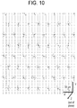
- the length of the area of the substrate affected when view in the XZ or YZ plane of FIG. 10 is from about 5 ⁇ m to about 150 ⁇ m, about 10 ⁇ m to about 120 ⁇ m, about 10 ⁇ m to about 100 ⁇ m, or about 20 ⁇ m to about 80 ⁇ m.
- the scattering features have a diameter of about 10, 20, 30, 40, 50, 60, 70, 80, 90, or 100 ⁇ m.
- the substrate is generally a sheet having two dimensions (e.g., X and Y) much larger than the third dimension (Z).
- Such substrates can have a thickness, Z, of any useful value.
- glass and polymer can have different structural advantages - the polymers often being less likely to break, but having less structural rigidity and strength.
- the substrate has a thickness of from about 3 mm to about 0.2 mm, about 2 mm to about 0.5 mm, or about 1 mm to about 0.7 mm. In some embodiments, the substrate has a thickness of about 0.1, 0.2, 0.3, 0.4, 0.5, 0.6, 0.7, 0.8, 0.9, 1, 2, or 3 mm.
- glass compositions that may be used generally comprise any composition that can be formed into a sheet by methods known in the art, including float, and fusion or other draw processes.
- alkali aluminosilicate glasses such as Corning Incorporated's GORILLA GLASS®
- display glasses such as Corning Incorporated's EAGLE XG®.
- the glass substrate may be chemically or thermally tempered prior to undergoing incorporation of the scattering centers.
- Glasses like Corning Incorporated's GORILLA GLASS® can be chemically tempered via ion-exchange techniques known in the art (see, e.g., U.S. Patent No. 5,674,790 , herein incorporated by reference in its entirety).
- ion-exchanged glass substrate it may be advantageous to place the scattering features in the central tension region of the glass.
- the scattering features are located within the central 1/3 of the glass substrate. In some embodiments, the scattering features are located within the central 1/5 of the glass substrate.
- Patterning of the scattering features in the substrate can be in any formation, such as arrays, geometries, random, etc. Patterns can be formed by translating either the laser or the laser beam, the substrate, or both, either manually or more efficiently via computer-aided techniques - techniques all well known by one of skill in the art. Placement or patterning of the scattering features on the substrate is only practically limited by the need that the scattering centers are sufficiently far apart to avoid causing substantial likelihood of crack propagation from one scattering feature to another. In some embodiments, the scattering features are from about 5 ⁇ m to about 2 mm apart (edge-to-edge of scattering features).
- the scattering features are about 5, 10, 15, 20, 25, 30, 40, 50, 60, 70, 80, 100, 150, 200, 500, 1000, 2000 ⁇ m apart (edge-to-edge of scattering features).
- TABLE 1 shows the density of scattering centers that can be obtained as a function of the spacing of the features.
- FIG. 2 shows an example of a LCD color array.
- the array comprises picture element ("A") that comprise red, green and blue pixels ("B"). Additionally, the pixels are separated by a black grid that in traditional backlight applications can block or absorb as much as 70% of the incident light.
- A picture element
- B red, green and blue pixels
- the scattering features By placing the scattering features in alignment with the transparent RGB subpixels, more light is transmitted because the light emitted by each individual extraction feature illuminates a specific RGB sub-pixel directly. This precise placement of the scattering features increases lighting efficiency by minimizing the extracted light blocked by boundary regions, which translates directly to lowering energy consumption and/or battery life in a display device.
- the scattering substrate formed by the incorporation of scattering features into the substrate shows a number of advantages over alternative methods of extracting light from a substrate.
- BLU backlight unit
- the laser-induced features are created directly in the substrate whereas other techniques involve applying an ink or polymer layer to the glass, which would normally contain the pattern. Accordingly, the substrate can in some embodiments be produced without a separate light extraction layer of material applied to the substrate.
- patterning in the glass substrate preserves the attributes of an all-glass system: (1) low roughness of fusion-drawn glass surface; (2) low H 2 0 absorption; (3) low CTE and no CTE mismatch issues; (4) high dimensional stability; (5) higher stiffness; (6) higher T g ; and (7) low thickness variation.
- the scattering substrate can be incorporated as a backlight into an electronic device, such as a tablet, smart phone, or television or computer display.
- the scattering substrate may incorporate one or more further modifications to improve its applicability.
- the light scattering features may produce "lining" or lines of brighter and darker areas in a display.
- one or both of the surfaces of the scattering substrate may be modified. These modifications can include, for example, one or more polymer or inorganic films, polymer or inorganic masks, or texturing, modifying, or roughening the surface of the substrate.
- scattering substrate surface modifications some embodiments involve the formation of a sub-micron structured surface having features on the nano- or picometer scale.
- the scattering substrate further comprises a nanostructured surface that provides additional light scattering properties. These features may be formed by any process known in the art, including negative or removal processes such as etching, and positive or additive processes like coating. Further, these features may be randomly place on the surface or may be placed in an organized or arrayed manner to complement the scattering features in the glass.
- the glass composition can play a role in the color composition of the scattered light. This is particularly important in large displays where uneven color scattering can cause changes in the color of the output light as a function of distance from the input LEDs.
- the glass substrate can be chosen to minimize compounds in it that absorb in the near-visible region. Such compounds include, but aren't limited to, iron compounds, sulfur compounds, manganese compounds, copper compounds, nickel compounds, chromium compounds, etc.
- the glass substrate comprises a low-iron glass, and in some embodiments, the glass comprises less than 50 ppm iron oxides, or less than 20 ppm iron oxides, such as FeO and Fe 2 O 3 .
- EXAMPLE 1 Laser-induced light scattering features described herein are created using a nanosecond pulsed Nd:YAG laser at 355 nm.
- the laser is focused to a 2-3 ⁇ m spot size inside a non-ion exchanged alkali aluminosilicate glass using an effective focal distance of 30 mm to create a damage spot within the glass which scatters light. While a non-ion exchanged alkali aluminosilicate glass was used in the experiments, the absorption of the glass is irrelevant to this process, allowing any glass that allows internal focusing to be used. At the focus, nearly all of the power of each pulse of the laser is absorbed by the glass to form what appears to be a tubular, melted region approximately 2-3 ⁇ m in diameter.
- the intensity of the laser is such that in addition to the formation of a melted region, a region of high stress and dislocated glass is formed in the surrounding glass structure.
- This stress can cause the formation of radial "microcracks" around the tube in all directions (see FIG. 10 , wherein the microcracks are approximately 20 ⁇ m).
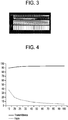
- the scattering features are nearly transparent when not illuminated and further, create a minimal amount of haze when not illuminated. This is shown in FIG. 4 , which compares haze (Y-axis) and transmittance (Y-axis) to scattering feature spacing (X-axis), and TABLE 2, below.
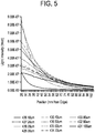
- EXAMPLE 3 Attenuation measurements are taken by injecting light into the edge of the glass and then measuring the amount of radiation coming out at 90° versus the distance from the light injection point. At the highest density of features (10 ⁇ m x 10 ⁇ m, 1,000,000 per cm 2 ), all of the light is extracted by ⁇ 50 mm into the glass.
- the next dense sample (20 ⁇ m x 10 ⁇ m, 500,000 per cm 2 ) extracts all of the light by ⁇ 80 mm into the glass.
- the density dropped the amount of light extracted near the light injection edge of the glass decreases, while the amount of light available farther from the edge of the glass increases ( see FIG. 5 , which shows 10, 20, 25, 30, 40, 50, 60, 70, 80, 90, and 100 ⁇ m x 10 ⁇ m densities of scattering features plotted as light intensity (W) versus position from the light injection edge in millimeters (mm)).
- W light intensity
- mm millimeters
- a gradient of features can be setup to extract an even amount of light across a 2" x 2" area of 0.7 non-ion exchanged alkali aluminosilicate glass.
- Attenuation data is collected from the sample to show a nearly even gradient of light extraction.
- Feature density starts at 207,000 points/cm 2 at the light injection edge and ends at 73,000 points/cm 2 at the far edge.
- Attenuation data is collected from the sample to show a nearly even gradient of light extraction ( FIG. 9 ).
- the gradient of light extraction can be affected by either point density or laser power, as noted above.
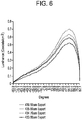
- the imaging sphere is a coated, diffuse, low-reflective hemisphere with a CCD-based photometer or colorimeter on the hemisphere and facing a convex mirror on the base of the sphere next to an illumination source (e.g., an LED, scattering substrate, etc.).
- an illumination source e.g., an LED, scattering substrate, etc.
- the source illuminates the interior surface of the hemisphere, and the mirror allows the detector to view essentially all of the 2 ⁇ steradian output.
- example scattering substrates show a maximum viewing angle of approximately 57 degrees, with a maximum of 0.7 Cd/cm 2 (7000 Nits) ( FIG. 6 ).
- Luminance measurements are taken for red, green, and blue individually ( FIG. 7 ).
- Color shift is calculated manually using CIE tristimulus calculations and graphically illustrated using tristimulus values for 60 and 70 ⁇ m scattering feature spacings ( FIGS. 8A and 8B , respectively).
- CIE 1931 x-values range from 0.310 to 0.314, well within industrial guidelines of 0.313 +/- 0.005.
- CIE 1931 y-values range from 0.306 to 0.309, slightly below industrial guidelines of 0.329 +/- 0.005.
- EXAMPLE 5 Glass substrate strength is impacted by the laser-featuring process as shown in ring-on-ring strength testing of featured 0.7 mm non-ion exchanged alkali aluminosilicate glass ( FIG. 11 ). The shape value increases from 1.591 for control samples to 7.118 for 20 ⁇ m x 20 ⁇ m spaced features and 5.061 for 40 ⁇ m x 40 ⁇ m spaced features, indicating a single mode of cracking.
- the scale value decreases from 188.5 for control samples to 84.91 for 20 ⁇ m x 20 ⁇ m spaced features and 70.16 for 40 ⁇ m x 40 ⁇ m spaced features, indicating more than a 50 percent drop in strength. While these values seem to indicate a significant strength drop, glass used internally as a backlight unit in a display device and contained within a mechanical structure would likely have reduced strength requirements versus a cover glass. Additional efforts, such as tempering, could be utilized to increase the strength of the samples after creating the scattering sites and thus this strength reduction might be ameliorated with post processing.
- Example 6 Low-loss, highly transparent glasses (e.g., ultra low-iron glasses - e.g., less than 50 ppm or less than 20 ppm iron oxides), are ideal for scattering substrate applications, due to their high transmittance with less color shift.
- measuring the loss in such glasses can be a challenge, especially where the substrate has been modified with laser-induced features.
- a scattering substrate comprising a sheet having two faces and at least two, opposite edges, it is possible to measure the loss via the following process:
Landscapes
- Physics & Mathematics (AREA)
- Optics & Photonics (AREA)
- General Physics & Mathematics (AREA)
- Engineering & Computer Science (AREA)
- Manufacturing & Machinery (AREA)
- Chemical & Material Sciences (AREA)
- Materials Engineering (AREA)
- Life Sciences & Earth Sciences (AREA)
- Health & Medical Sciences (AREA)
- Chemical Kinetics & Catalysis (AREA)
- General Chemical & Material Sciences (AREA)
- Geochemistry & Mineralogy (AREA)
- Toxicology (AREA)
- Organic Chemistry (AREA)
- Laser Beam Processing (AREA)
- Glass Compositions (AREA)
- Surface Treatment Of Glass (AREA)
- Optical Elements Other Than Lenses (AREA)
- Planar Illumination Modules (AREA)
Applications Claiming Priority (2)
| Application Number | Priority Date | Filing Date | Title |
|---|---|---|---|
| US201461933064P | 2014-01-29 | 2014-01-29 | |
| PCT/US2015/013390 WO2015116743A1 (en) | 2014-01-29 | 2015-01-29 | Laser featured glass for display illumination |
Publications (2)
| Publication Number | Publication Date |
|---|---|
| EP3100081A1 EP3100081A1 (en) | 2016-12-07 |
| EP3100081B1 true EP3100081B1 (en) | 2020-03-11 |
Family
ID=52597253
Family Applications (1)
| Application Number | Title | Priority Date | Filing Date |
|---|---|---|---|
| EP15707449.3A Active EP3100081B1 (en) | 2014-01-29 | 2015-01-29 | Laser modified glass for display illumination |
Country Status (7)
Families Citing this family (9)
| Publication number | Priority date | Publication date | Assignee | Title |
|---|---|---|---|---|
| CN107771169A (zh) * | 2015-05-18 | 2018-03-06 | 康宁股份有限公司 | 包含光提取特征的玻璃制品及其制造方法 |
| US10207950B2 (en) * | 2015-09-25 | 2019-02-19 | Lg Chem, Ltd. | Glass light guiding plate |
| EP3436415A1 (en) * | 2016-03-29 | 2019-02-06 | Corning Incorporated | Glass articles comprising light extraction features and methods for making the same |
| EP3228931A1 (de) * | 2016-04-04 | 2017-10-11 | Weidplas GmbH | Lichtleiter mit lichtumlenkstrukturen |
| WO2018094017A1 (en) | 2016-11-18 | 2018-05-24 | Corning Incorporated | Microstructured light guide plates and devices comprising the same |
| CN110140009B (zh) * | 2016-12-29 | 2022-02-25 | 康宁股份有限公司 | 微结构化和图案化光导板及包含该光导板的装置 |
| US11014497B2 (en) | 2017-07-21 | 2021-05-25 | Weidplas Gmbh | Component for a vehicle |
| EP3679958A1 (de) | 2019-01-09 | 2020-07-15 | Medela Holding AG | Saugpumpe mit optischem statusindikator |
| EE05853B1 (et) * | 2021-05-09 | 2023-05-15 | Jevgeni Berik | Meetod ja seade läbipaistvate objektide pealispinna desinfitseerimiseks UV-kiirguse abil |
Family Cites Families (46)
| Publication number | Priority date | Publication date | Assignee | Title |
|---|---|---|---|---|
| US5030594A (en) * | 1990-06-29 | 1991-07-09 | Ppg Industries, Inc. | Highly transparent, edge colored glass |
| IL99170A0 (en) | 1990-08-15 | 1992-07-15 | United Distillers Plc | Method and apparatus for sub-surface marking |
| US5339179A (en) | 1992-10-01 | 1994-08-16 | International Business Machines Corp. | Edge-lit transflective non-emissive display with angled interface means on both sides of light conducting panel |
| US5637244A (en) | 1993-05-13 | 1997-06-10 | Podarok International, Inc. | Method and apparatus for creating an image by a pulsed laser beam inside a transparent material |
| US5674790A (en) | 1995-12-15 | 1997-10-07 | Corning Incorporated | Strengthening glass by ion exchange |
| US7364072B1 (en) | 1996-01-02 | 2008-04-29 | Steven Jerome Moore | Apparatus and method for security |
| US6392683B1 (en) | 1997-09-26 | 2002-05-21 | Sumitomo Heavy Industries, Ltd. | Method for making marks in a transparent material by using a laser |
| JP2000113708A (ja) * | 1998-10-02 | 2000-04-21 | Toshiba Chem Corp | 照明装置 |
| JP3527961B2 (ja) * | 1999-04-30 | 2004-05-17 | 株式会社日立製作所 | フロントライト型反射液晶表示装置 |
| US6333486B1 (en) * | 2000-04-25 | 2001-12-25 | Igor Troitski | Method and laser system for creation of laser-induced damages to produce high quality images |
| JP2002062438A (ja) * | 2000-08-17 | 2002-02-28 | Tamura Electric Works Ltd | 導光体及び照明装置 |
| TW503188B (en) | 2000-08-29 | 2002-09-21 | Sumitomo Heavy Industries | Marking method, device the optical member marked |
| US20020186924A1 (en) | 2001-02-22 | 2002-12-12 | Kohnke Glenn E. | Grating fabrication method and apparatus |
| US6768080B2 (en) | 2001-12-17 | 2004-07-27 | Troitski | Method for production of laser-induced damage images with special characteristics by creating damages of special space shape |
| US6727460B2 (en) | 2002-02-14 | 2004-04-27 | Troitski | System for high-speed production of high quality laser-induced damage images inside transparent materials |
| DE10222250A1 (de) * | 2002-05-16 | 2003-11-27 | Roehm Gmbh | Verbesserte Lichtleitkörper sowie Verfahren zu dessen Herstellung |
| JP2005025972A (ja) * | 2003-06-30 | 2005-01-27 | Fujitsu Kasei Kk | 面照明装置と液晶表示装置 |
| JP2005158370A (ja) | 2003-11-21 | 2005-06-16 | Toyota Industries Corp | 面状光源装置及び液晶表示装置 |
| JP2006159937A (ja) * | 2004-12-02 | 2006-06-22 | Toyota Motor Corp | 車両のブレーキ装置 |
| CN1786745A (zh) | 2004-12-11 | 2006-06-14 | 群康科技(深圳)有限公司 | 导光板制造方法 |
| DE102005041242A1 (de) * | 2005-08-31 | 2007-03-01 | Merck Patent Gmbh | Verfahren zur Strukturierung von Oberflächen von Substraten |
| DK1979889T3 (da) * | 2006-01-12 | 2012-09-10 | Ppg Ind Ohio Inc | Displaypanel, som har laserinduceret lysomdirigeringstræk |
| CN101470230A (zh) * | 2007-12-29 | 2009-07-01 | 上海边光实业有限公司 | 一种利用激光脉冲雕刻的导光板及其制备方法 |
| TW200935094A (en) | 2008-02-05 | 2009-08-16 | Kismart Corp | A method of forming light-scattering dots inside the diffusion plate and light guide plate by laser engraving |
| JP5405763B2 (ja) | 2008-03-28 | 2014-02-05 | 日東電工株式会社 | 指向性拡散フィルム、偏光板、液晶表示装置および指向性拡散フィルムの製造方法 |
| US8304358B2 (en) | 2008-11-21 | 2012-11-06 | Ppg Industries Ohio, Inc. | Method of reducing redox ratio of molten glass and the glass made thereby |
| CN101462825B (zh) * | 2008-12-30 | 2011-02-16 | 中国南玻集团股份有限公司 | 超白浮法玻璃 |
| KR20110121605A (ko) * | 2009-02-02 | 2011-11-07 | 아사히 가라스 가부시키가이샤 | 반도체 디바이스 부재용 유리 기판 및 반도체 디바이스 부재용 유리 기판의 제조 방법 |
| JP5616907B2 (ja) * | 2009-03-02 | 2014-10-29 | アップル インコーポレイテッド | ポータブル電子デバイスのガラスカバーを強化する技術 |
| CN101554817A (zh) | 2009-04-30 | 2009-10-14 | 达运精密工业(苏州)有限公司 | 一种扩散板的加工方法及其扩散板 |
| JP5493654B2 (ja) | 2009-09-29 | 2014-05-14 | 日亜化学工業株式会社 | 導光板、及びその導光板を備える面光源装置 |
| CN102219375A (zh) | 2010-04-16 | 2011-10-19 | 信义光伏产业(安徽)控股有限公司 | 太阳能超白压延玻璃及其制备方法 |
| CN101867020A (zh) | 2010-06-01 | 2010-10-20 | 友达光电股份有限公司 | 发光元件 |
| US9529228B2 (en) * | 2010-11-05 | 2016-12-27 | Yissum Research Development Company Of The Hebrew University Of Jerusalem, Ltd. | Polarizing lighting systems |
| CN102062893A (zh) | 2010-11-11 | 2011-05-18 | 深圳安嵘光电产品有限公司 | 一种内雕刻制作的导光板及其制作方法、照明灯具 |
| CN103237771B (zh) * | 2010-11-30 | 2016-10-19 | 康宁股份有限公司 | 在玻璃中形成高密度孔阵列的方法 |
| CN102179628A (zh) | 2011-03-18 | 2011-09-14 | 上海理工大学 | 导光板激光式雕刻设备及其使用方法 |
| CN202049254U (zh) | 2011-04-01 | 2011-11-23 | 冠捷投资有限公司 | 一种具有激光内雕之导光板结构 |
| US8789998B2 (en) * | 2011-08-31 | 2014-07-29 | Corning Incorporated | Edge illumination of an ion-exchanged glass sheet |
| BE1020296A3 (fr) | 2011-11-15 | 2013-07-02 | Agc Glass Europe | Feuille de verre a haute transmission energetique. |
| CN202494800U (zh) | 2012-03-23 | 2012-10-17 | 京东方科技集团股份有限公司 | 导光板、背光源及显示装置 |
| EP2841847B1 (en) | 2012-04-26 | 2018-11-21 | Philips Lighting Holding B.V. | Lighting arrangement |
| US8926143B2 (en) * | 2013-03-13 | 2015-01-06 | Corning Incorporated | Light-diffusing elements |
| DE102014205066A1 (de) * | 2014-03-19 | 2015-10-08 | Schott Ag | Vorgespannter Glasartikel mit Laserinnengravur und Herstellverfahren |
| KR102056359B1 (ko) * | 2016-05-03 | 2019-12-16 | 주식회사 엘지화학 | 붕규산 유리, 이것을 포함하는 도광판 및 그 제조 방법 |
| KR102058195B1 (ko) * | 2016-06-13 | 2019-12-20 | 주식회사 엘지화학 | 유리 도광판 및 그 제조 방법 |
-
2015
- 2015-01-29 KR KR1020167023149A patent/KR20160113658A/ko not_active Withdrawn
- 2015-01-29 CN CN201580006540.3A patent/CN105940323B/zh not_active Expired - Fee Related
- 2015-01-29 US US15/114,675 patent/US10288792B2/en not_active Expired - Fee Related
- 2015-01-29 WO PCT/US2015/013390 patent/WO2015116743A1/en active Application Filing
- 2015-01-29 EP EP15707449.3A patent/EP3100081B1/en active Active
- 2015-01-29 JP JP2016548650A patent/JP2017507103A/ja active Pending
- 2015-01-29 TW TW104103088A patent/TWI641874B/zh not_active IP Right Cessation
Non-Patent Citations (1)
| Title |
|---|
| None * |
Also Published As
| Publication number | Publication date |
|---|---|
| EP3100081A1 (en) | 2016-12-07 |
| CN105940323A (zh) | 2016-09-14 |
| TWI641874B (zh) | 2018-11-21 |
| US10288792B2 (en) | 2019-05-14 |
| TW201534987A (zh) | 2015-09-16 |
| KR20160113658A (ko) | 2016-09-30 |
| US20160349440A1 (en) | 2016-12-01 |
| JP2017507103A (ja) | 2017-03-16 |
| WO2015116743A1 (en) | 2015-08-06 |
| CN105940323B (zh) | 2019-07-12 |
Similar Documents
| Publication | Publication Date | Title |
|---|---|---|
| EP3100081B1 (en) | Laser modified glass for display illumination | |
| US11067735B2 (en) | Direct-lit backlight unit with 2D local dimming | |
| CN105163949B (zh) | 用于改变玻璃和玻璃陶瓷透射的方法以及能够根据该方法制造的玻璃件或玻璃陶瓷件 | |
| KR101064859B1 (ko) | 디스플레이 디바이스 및 디스플레이 패널 제작 방법 | |
| KR102637705B1 (ko) | 직접 조명 백라이트들을 위한 다중층 반사부 | |
| US11022745B2 (en) | Microstructured and patterned light guide plates and devices comprising the same | |
| US20190146139A1 (en) | Microstructured and patterned light guide plates and devices comprising the same | |
| KR102450088B1 (ko) | 미세 구조화된 도광판 및 그를 포함하는 장치 | |
| CN101963315B (zh) | 光源模块与液晶显示器 | |
| US20190146140A1 (en) | Glass articles comprising light extraction features | |
| KR20170016927A (ko) | 패턴된 유리 광 가이드 및 이를 포함하는 디스플레이 장치 | |
| KR20190112168A (ko) | 일체형 백라이트 유닛 및 디스플레이 패널을 포함하는 장치 | |
| US20200399175A1 (en) | Glass articles comprising light extraction features and methods for making the same | |
| KR20180124131A (ko) | 국부적으로 디밍가능한 광 가이드 플레이트들 및 이를 포함하는 디스플레이 장치들 | |
| WO2019217408A1 (en) | Backlight unit with improved 2d local dimming | |
| CN102466900A (zh) | 平面显示器的修补方法与系统 | |
| Liu et al. | Propagation of a filamentary femtosecond laser beam with high intensities at an air-solid interface | |
| CN107646092A (zh) | 用于对显示面板进行照明的玻璃制品 |
Legal Events
| Date | Code | Title | Description |
|---|---|---|---|
| PUAI | Public reference made under article 153(3) epc to a published international application that has entered the european phase |
Free format text: ORIGINAL CODE: 0009012 |
|
| STAA | Information on the status of an ep patent application or granted ep patent |
Free format text: STATUS: REQUEST FOR EXAMINATION WAS MADE |
|
| 17P | Request for examination filed |
Effective date: 20160825 |
|
| AK | Designated contracting states |
Kind code of ref document: A1 Designated state(s): AL AT BE BG CH CY CZ DE DK EE ES FI FR GB GR HR HU IE IS IT LI LT LU LV MC MK MT NL NO PL PT RO RS SE SI SK SM TR |
|
| AX | Request for extension of the european patent |
Extension state: BA ME |
|
| DAX | Request for extension of the european patent (deleted) | ||
| STAA | Information on the status of an ep patent application or granted ep patent |
Free format text: STATUS: EXAMINATION IS IN PROGRESS |
|
| 17Q | First examination report despatched |
Effective date: 20190218 |
|
| GRAP | Despatch of communication of intention to grant a patent |
Free format text: ORIGINAL CODE: EPIDOSNIGR1 |
|
| STAA | Information on the status of an ep patent application or granted ep patent |
Free format text: STATUS: GRANT OF PATENT IS INTENDED |
|
| GRAS | Grant fee paid |
Free format text: ORIGINAL CODE: EPIDOSNIGR3 |
|
| INTG | Intention to grant announced |
Effective date: 20200113 |
|
| GRAA | (expected) grant |
Free format text: ORIGINAL CODE: 0009210 |
|
| STAA | Information on the status of an ep patent application or granted ep patent |
Free format text: STATUS: THE PATENT HAS BEEN GRANTED |
|
| AK | Designated contracting states |
Kind code of ref document: B1 Designated state(s): AL AT BE BG CH CY CZ DE DK EE ES FI FR GB GR HR HU IE IS IT LI LT LU LV MC MK MT NL NO PL PT RO RS SE SI SK SM TR |
|
| REG | Reference to a national code |
Ref country code: GB Ref legal event code: FG4D |
|
| REG | Reference to a national code |
Ref country code: CH Ref legal event code: EP |
|
| REG | Reference to a national code |
Ref country code: AT Ref legal event code: REF Ref document number: 1243868 Country of ref document: AT Kind code of ref document: T Effective date: 20200315 |
|
| REG | Reference to a national code |
Ref country code: IE Ref legal event code: FG4D |
|
| REG | Reference to a national code |
Ref country code: DE Ref legal event code: R096 Ref document number: 602015048535 Country of ref document: DE |
|
| PG25 | Lapsed in a contracting state [announced via postgrant information from national office to epo] |
Ref country code: RS Free format text: LAPSE BECAUSE OF FAILURE TO SUBMIT A TRANSLATION OF THE DESCRIPTION OR TO PAY THE FEE WITHIN THE PRESCRIBED TIME-LIMIT Effective date: 20200311 Ref country code: NO Free format text: LAPSE BECAUSE OF FAILURE TO SUBMIT A TRANSLATION OF THE DESCRIPTION OR TO PAY THE FEE WITHIN THE PRESCRIBED TIME-LIMIT Effective date: 20200611 Ref country code: FI Free format text: LAPSE BECAUSE OF FAILURE TO SUBMIT A TRANSLATION OF THE DESCRIPTION OR TO PAY THE FEE WITHIN THE PRESCRIBED TIME-LIMIT Effective date: 20200311 |
|
| REG | Reference to a national code |
Ref country code: NL Ref legal event code: MP Effective date: 20200311 |
|
| PG25 | Lapsed in a contracting state [announced via postgrant information from national office to epo] |
Ref country code: BG Free format text: LAPSE BECAUSE OF FAILURE TO SUBMIT A TRANSLATION OF THE DESCRIPTION OR TO PAY THE FEE WITHIN THE PRESCRIBED TIME-LIMIT Effective date: 20200611 Ref country code: SE Free format text: LAPSE BECAUSE OF FAILURE TO SUBMIT A TRANSLATION OF THE DESCRIPTION OR TO PAY THE FEE WITHIN THE PRESCRIBED TIME-LIMIT Effective date: 20200311 Ref country code: HR Free format text: LAPSE BECAUSE OF FAILURE TO SUBMIT A TRANSLATION OF THE DESCRIPTION OR TO PAY THE FEE WITHIN THE PRESCRIBED TIME-LIMIT Effective date: 20200311 Ref country code: LV Free format text: LAPSE BECAUSE OF FAILURE TO SUBMIT A TRANSLATION OF THE DESCRIPTION OR TO PAY THE FEE WITHIN THE PRESCRIBED TIME-LIMIT Effective date: 20200311 Ref country code: GR Free format text: LAPSE BECAUSE OF FAILURE TO SUBMIT A TRANSLATION OF THE DESCRIPTION OR TO PAY THE FEE WITHIN THE PRESCRIBED TIME-LIMIT Effective date: 20200612 |
|
| REG | Reference to a national code |
Ref country code: LT Ref legal event code: MG4D |
|
| PG25 | Lapsed in a contracting state [announced via postgrant information from national office to epo] |
Ref country code: NL Free format text: LAPSE BECAUSE OF FAILURE TO SUBMIT A TRANSLATION OF THE DESCRIPTION OR TO PAY THE FEE WITHIN THE PRESCRIBED TIME-LIMIT Effective date: 20200311 |
|
| PG25 | Lapsed in a contracting state [announced via postgrant information from national office to epo] |
Ref country code: SK Free format text: LAPSE BECAUSE OF FAILURE TO SUBMIT A TRANSLATION OF THE DESCRIPTION OR TO PAY THE FEE WITHIN THE PRESCRIBED TIME-LIMIT Effective date: 20200311 Ref country code: PT Free format text: LAPSE BECAUSE OF FAILURE TO SUBMIT A TRANSLATION OF THE DESCRIPTION OR TO PAY THE FEE WITHIN THE PRESCRIBED TIME-LIMIT Effective date: 20200805 Ref country code: IS Free format text: LAPSE BECAUSE OF FAILURE TO SUBMIT A TRANSLATION OF THE DESCRIPTION OR TO PAY THE FEE WITHIN THE PRESCRIBED TIME-LIMIT Effective date: 20200711 Ref country code: CZ Free format text: LAPSE BECAUSE OF FAILURE TO SUBMIT A TRANSLATION OF THE DESCRIPTION OR TO PAY THE FEE WITHIN THE PRESCRIBED TIME-LIMIT Effective date: 20200311 Ref country code: LT Free format text: LAPSE BECAUSE OF FAILURE TO SUBMIT A TRANSLATION OF THE DESCRIPTION OR TO PAY THE FEE WITHIN THE PRESCRIBED TIME-LIMIT Effective date: 20200311 Ref country code: RO Free format text: LAPSE BECAUSE OF FAILURE TO SUBMIT A TRANSLATION OF THE DESCRIPTION OR TO PAY THE FEE WITHIN THE PRESCRIBED TIME-LIMIT Effective date: 20200311 Ref country code: EE Free format text: LAPSE BECAUSE OF FAILURE TO SUBMIT A TRANSLATION OF THE DESCRIPTION OR TO PAY THE FEE WITHIN THE PRESCRIBED TIME-LIMIT Effective date: 20200311 Ref country code: SM Free format text: LAPSE BECAUSE OF FAILURE TO SUBMIT A TRANSLATION OF THE DESCRIPTION OR TO PAY THE FEE WITHIN THE PRESCRIBED TIME-LIMIT Effective date: 20200311 |
|
| REG | Reference to a national code |
Ref country code: AT Ref legal event code: MK05 Ref document number: 1243868 Country of ref document: AT Kind code of ref document: T Effective date: 20200311 |
|
| REG | Reference to a national code |
Ref country code: DE Ref legal event code: R097 Ref document number: 602015048535 Country of ref document: DE |
|
| PLBE | No opposition filed within time limit |
Free format text: ORIGINAL CODE: 0009261 |
|
| STAA | Information on the status of an ep patent application or granted ep patent |
Free format text: STATUS: NO OPPOSITION FILED WITHIN TIME LIMIT |
|
| PG25 | Lapsed in a contracting state [announced via postgrant information from national office to epo] |
Ref country code: AT Free format text: LAPSE BECAUSE OF FAILURE TO SUBMIT A TRANSLATION OF THE DESCRIPTION OR TO PAY THE FEE WITHIN THE PRESCRIBED TIME-LIMIT Effective date: 20200311 Ref country code: DK Free format text: LAPSE BECAUSE OF FAILURE TO SUBMIT A TRANSLATION OF THE DESCRIPTION OR TO PAY THE FEE WITHIN THE PRESCRIBED TIME-LIMIT Effective date: 20200311 Ref country code: ES Free format text: LAPSE BECAUSE OF FAILURE TO SUBMIT A TRANSLATION OF THE DESCRIPTION OR TO PAY THE FEE WITHIN THE PRESCRIBED TIME-LIMIT Effective date: 20200311 Ref country code: IT Free format text: LAPSE BECAUSE OF FAILURE TO SUBMIT A TRANSLATION OF THE DESCRIPTION OR TO PAY THE FEE WITHIN THE PRESCRIBED TIME-LIMIT Effective date: 20200311 |
|
| 26N | No opposition filed |
Effective date: 20201214 |
|
| PG25 | Lapsed in a contracting state [announced via postgrant information from national office to epo] |
Ref country code: PL Free format text: LAPSE BECAUSE OF FAILURE TO SUBMIT A TRANSLATION OF THE DESCRIPTION OR TO PAY THE FEE WITHIN THE PRESCRIBED TIME-LIMIT Effective date: 20200311 Ref country code: SI Free format text: LAPSE BECAUSE OF FAILURE TO SUBMIT A TRANSLATION OF THE DESCRIPTION OR TO PAY THE FEE WITHIN THE PRESCRIBED TIME-LIMIT Effective date: 20200311 |
|
| REG | Reference to a national code |
Ref country code: DE Ref legal event code: R119 Ref document number: 602015048535 Country of ref document: DE |
|
| PG25 | Lapsed in a contracting state [announced via postgrant information from national office to epo] |
Ref country code: MC Free format text: LAPSE BECAUSE OF FAILURE TO SUBMIT A TRANSLATION OF THE DESCRIPTION OR TO PAY THE FEE WITHIN THE PRESCRIBED TIME-LIMIT Effective date: 20200311 |
|
| REG | Reference to a national code |
Ref country code: CH Ref legal event code: PL |
|
| GBPC | Gb: european patent ceased through non-payment of renewal fee |
Effective date: 20210129 |
|
| PG25 | Lapsed in a contracting state [announced via postgrant information from national office to epo] |
Ref country code: LU Free format text: LAPSE BECAUSE OF NON-PAYMENT OF DUE FEES Effective date: 20210129 |
|
| REG | Reference to a national code |
Ref country code: BE Ref legal event code: MM Effective date: 20210131 |
|
| PG25 | Lapsed in a contracting state [announced via postgrant information from national office to epo] |
Ref country code: FR Free format text: LAPSE BECAUSE OF NON-PAYMENT OF DUE FEES Effective date: 20210131 |
|
| PG25 | Lapsed in a contracting state [announced via postgrant information from national office to epo] |
Ref country code: DE Free format text: LAPSE BECAUSE OF NON-PAYMENT OF DUE FEES Effective date: 20210803 Ref country code: CH Free format text: LAPSE BECAUSE OF NON-PAYMENT OF DUE FEES Effective date: 20210131 Ref country code: LI Free format text: LAPSE BECAUSE OF NON-PAYMENT OF DUE FEES Effective date: 20210131 Ref country code: GB Free format text: LAPSE BECAUSE OF NON-PAYMENT OF DUE FEES Effective date: 20210129 |
|
| PG25 | Lapsed in a contracting state [announced via postgrant information from national office to epo] |
Ref country code: IE Free format text: LAPSE BECAUSE OF NON-PAYMENT OF DUE FEES Effective date: 20210129 |
|
| PG25 | Lapsed in a contracting state [announced via postgrant information from national office to epo] |
Ref country code: BE Free format text: LAPSE BECAUSE OF NON-PAYMENT OF DUE FEES Effective date: 20210131 |
|
| PG25 | Lapsed in a contracting state [announced via postgrant information from national office to epo] |
Ref country code: HU Free format text: LAPSE BECAUSE OF FAILURE TO SUBMIT A TRANSLATION OF THE DESCRIPTION OR TO PAY THE FEE WITHIN THE PRESCRIBED TIME-LIMIT; INVALID AB INITIO Effective date: 20150129 |
|
| PG25 | Lapsed in a contracting state [announced via postgrant information from national office to epo] |
Ref country code: CY Free format text: LAPSE BECAUSE OF FAILURE TO SUBMIT A TRANSLATION OF THE DESCRIPTION OR TO PAY THE FEE WITHIN THE PRESCRIBED TIME-LIMIT Effective date: 20200311 |
|
| PG25 | Lapsed in a contracting state [announced via postgrant information from national office to epo] |
Ref country code: MK Free format text: LAPSE BECAUSE OF FAILURE TO SUBMIT A TRANSLATION OF THE DESCRIPTION OR TO PAY THE FEE WITHIN THE PRESCRIBED TIME-LIMIT Effective date: 20200311 |
|
| PG25 | Lapsed in a contracting state [announced via postgrant information from national office to epo] |
Ref country code: TR Free format text: LAPSE BECAUSE OF FAILURE TO SUBMIT A TRANSLATION OF THE DESCRIPTION OR TO PAY THE FEE WITHIN THE PRESCRIBED TIME-LIMIT Effective date: 20200311 |
|
| PG25 | Lapsed in a contracting state [announced via postgrant information from national office to epo] |
Ref country code: MT Free format text: LAPSE BECAUSE OF FAILURE TO SUBMIT A TRANSLATION OF THE DESCRIPTION OR TO PAY THE FEE WITHIN THE PRESCRIBED TIME-LIMIT Effective date: 20200311 |