EP3093877A2 - Semiconductor package and fabrication method thereof - Google Patents
Semiconductor package and fabrication method thereof Download PDFInfo
- Publication number
- EP3093877A2 EP3093877A2 EP16161578.6A EP16161578A EP3093877A2 EP 3093877 A2 EP3093877 A2 EP 3093877A2 EP 16161578 A EP16161578 A EP 16161578A EP 3093877 A2 EP3093877 A2 EP 3093877A2
- Authority
- EP
- European Patent Office
- Prior art keywords
- encapsulant
- semiconductor package
- semiconductor
- further characterized
- semiconductor die
- Prior art date
- Legal status (The legal status is an assumption and is not a legal conclusion. Google has not performed a legal analysis and makes no representation as to the accuracy of the status listed.)
- Granted
Links
Images







Classifications
-
- H—ELECTRICITY
- H10—SEMICONDUCTOR DEVICES; ELECTRIC SOLID-STATE DEVICES NOT OTHERWISE PROVIDED FOR
- H10W—GENERIC PACKAGES, INTERCONNECTIONS, CONNECTORS OR OTHER CONSTRUCTIONAL DETAILS OF DEVICES COVERED BY CLASS H10
- H10W90/00—Package configurations
-
- H—ELECTRICITY
- H10—SEMICONDUCTOR DEVICES; ELECTRIC SOLID-STATE DEVICES NOT OTHERWISE PROVIDED FOR
- H10W—GENERIC PACKAGES, INTERCONNECTIONS, CONNECTORS OR OTHER CONSTRUCTIONAL DETAILS OF DEVICES COVERED BY CLASS H10
- H10W70/00—Package substrates; Interposers; Redistribution layers [RDL]
- H10W70/01—Manufacture or treatment
- H10W70/04—Manufacture or treatment of leadframes
- H10W70/042—Etching
-
- H—ELECTRICITY
- H10—SEMICONDUCTOR DEVICES; ELECTRIC SOLID-STATE DEVICES NOT OTHERWISE PROVIDED FOR
- H10W—GENERIC PACKAGES, INTERCONNECTIONS, CONNECTORS OR OTHER CONSTRUCTIONAL DETAILS OF DEVICES COVERED BY CLASS H10
- H10W70/00—Package substrates; Interposers; Redistribution layers [RDL]
- H10W70/01—Manufacture or treatment
- H10W70/05—Manufacture or treatment of insulating or insulated package substrates, or of interposers, or of redistribution layers
- H10W70/08—Manufacture or treatment of insulating or insulated package substrates, or of interposers, or of redistribution layers by depositing layers on the chip or wafer, e.g. "chip-first" RDLs
- H10W70/09—Manufacture or treatment of insulating or insulated package substrates, or of interposers, or of redistribution layers by depositing layers on the chip or wafer, e.g. "chip-first" RDLs extending onto an encapsulation that laterally surrounds the chip or wafer, e.g. fan-out wafer level package [FOWLP] RDLs
-
- H—ELECTRICITY
- H10—SEMICONDUCTOR DEVICES; ELECTRIC SOLID-STATE DEVICES NOT OTHERWISE PROVIDED FOR
- H10W—GENERIC PACKAGES, INTERCONNECTIONS, CONNECTORS OR OTHER CONSTRUCTIONAL DETAILS OF DEVICES COVERED BY CLASS H10
- H10W70/00—Package substrates; Interposers; Redistribution layers [RDL]
- H10W70/60—Insulating or insulated package substrates; Interposers; Redistribution layers
-
- H—ELECTRICITY
- H10—SEMICONDUCTOR DEVICES; ELECTRIC SOLID-STATE DEVICES NOT OTHERWISE PROVIDED FOR
- H10W—GENERIC PACKAGES, INTERCONNECTIONS, CONNECTORS OR OTHER CONSTRUCTIONAL DETAILS OF DEVICES COVERED BY CLASS H10
- H10W70/00—Package substrates; Interposers; Redistribution layers [RDL]
- H10W70/60—Insulating or insulated package substrates; Interposers; Redistribution layers
- H10W70/611—Insulating or insulated package substrates; Interposers; Redistribution layers for connecting multiple chips together
- H10W70/614—Insulating or insulated package substrates; Interposers; Redistribution layers for connecting multiple chips together the multiple chips being integrally enclosed
-
- H—ELECTRICITY
- H10—SEMICONDUCTOR DEVICES; ELECTRIC SOLID-STATE DEVICES NOT OTHERWISE PROVIDED FOR
- H10W—GENERIC PACKAGES, INTERCONNECTIONS, CONNECTORS OR OTHER CONSTRUCTIONAL DETAILS OF DEVICES COVERED BY CLASS H10
- H10W72/00—Interconnections or connectors in packages
- H10W72/01—Manufacture or treatment
- H10W72/015—Manufacture or treatment of bond wires
-
- H—ELECTRICITY
- H10—SEMICONDUCTOR DEVICES; ELECTRIC SOLID-STATE DEVICES NOT OTHERWISE PROVIDED FOR
- H10W—GENERIC PACKAGES, INTERCONNECTIONS, CONNECTORS OR OTHER CONSTRUCTIONAL DETAILS OF DEVICES COVERED BY CLASS H10
- H10W72/00—Interconnections or connectors in packages
- H10W72/01—Manufacture or treatment
- H10W72/019—Manufacture or treatment of bond pads
-
- H—ELECTRICITY
- H10—SEMICONDUCTOR DEVICES; ELECTRIC SOLID-STATE DEVICES NOT OTHERWISE PROVIDED FOR
- H10W—GENERIC PACKAGES, INTERCONNECTIONS, CONNECTORS OR OTHER CONSTRUCTIONAL DETAILS OF DEVICES COVERED BY CLASS H10
- H10W72/00—Interconnections or connectors in packages
- H10W72/20—Bump connectors, e.g. solder bumps or copper pillars; Dummy bumps; Thermal bumps
-
- H—ELECTRICITY
- H10—SEMICONDUCTOR DEVICES; ELECTRIC SOLID-STATE DEVICES NOT OTHERWISE PROVIDED FOR
- H10W—GENERIC PACKAGES, INTERCONNECTIONS, CONNECTORS OR OTHER CONSTRUCTIONAL DETAILS OF DEVICES COVERED BY CLASS H10
- H10W72/00—Interconnections or connectors in packages
- H10W72/50—Bond wires
-
- H—ELECTRICITY
- H10—SEMICONDUCTOR DEVICES; ELECTRIC SOLID-STATE DEVICES NOT OTHERWISE PROVIDED FOR
- H10W—GENERIC PACKAGES, INTERCONNECTIONS, CONNECTORS OR OTHER CONSTRUCTIONAL DETAILS OF DEVICES COVERED BY CLASS H10
- H10W72/00—Interconnections or connectors in packages
- H10W72/90—Bond pads, in general
-
- H—ELECTRICITY
- H10—SEMICONDUCTOR DEVICES; ELECTRIC SOLID-STATE DEVICES NOT OTHERWISE PROVIDED FOR
- H10W—GENERIC PACKAGES, INTERCONNECTIONS, CONNECTORS OR OTHER CONSTRUCTIONAL DETAILS OF DEVICES COVERED BY CLASS H10
- H10W74/00—Encapsulations, e.g. protective coatings
- H10W74/01—Manufacture or treatment
- H10W74/012—Manufacture or treatment of encapsulations on active surfaces of flip-chip devices, e.g. forming underfills
-
- H—ELECTRICITY
- H10—SEMICONDUCTOR DEVICES; ELECTRIC SOLID-STATE DEVICES NOT OTHERWISE PROVIDED FOR
- H10W—GENERIC PACKAGES, INTERCONNECTIONS, CONNECTORS OR OTHER CONSTRUCTIONAL DETAILS OF DEVICES COVERED BY CLASS H10
- H10W74/00—Encapsulations, e.g. protective coatings
- H10W74/01—Manufacture or treatment
- H10W74/014—Manufacture or treatment using batch processing
-
- H—ELECTRICITY
- H10—SEMICONDUCTOR DEVICES; ELECTRIC SOLID-STATE DEVICES NOT OTHERWISE PROVIDED FOR
- H10W—GENERIC PACKAGES, INTERCONNECTIONS, CONNECTORS OR OTHER CONSTRUCTIONAL DETAILS OF DEVICES COVERED BY CLASS H10
- H10W74/00—Encapsulations, e.g. protective coatings
- H10W74/10—Encapsulations, e.g. protective coatings characterised by their shape or disposition
- H10W74/15—Encapsulations, e.g. protective coatings characterised by their shape or disposition on active surfaces of flip-chip devices, e.g. underfills
-
- H—ELECTRICITY
- H10—SEMICONDUCTOR DEVICES; ELECTRIC SOLID-STATE DEVICES NOT OTHERWISE PROVIDED FOR
- H10W—GENERIC PACKAGES, INTERCONNECTIONS, CONNECTORS OR OTHER CONSTRUCTIONAL DETAILS OF DEVICES COVERED BY CLASS H10
- H10W74/00—Encapsulations, e.g. protective coatings
- H10W74/40—Encapsulations, e.g. protective coatings characterised by their materials
- H10W74/47—Encapsulations, e.g. protective coatings characterised by their materials comprising organic materials, e.g. plastics or resins
-
- H—ELECTRICITY
- H10—SEMICONDUCTOR DEVICES; ELECTRIC SOLID-STATE DEVICES NOT OTHERWISE PROVIDED FOR
- H10W—GENERIC PACKAGES, INTERCONNECTIONS, CONNECTORS OR OTHER CONSTRUCTIONAL DETAILS OF DEVICES COVERED BY CLASS H10
- H10W70/00—Package substrates; Interposers; Redistribution layers [RDL]
- H10W70/01—Manufacture or treatment
- H10W70/05—Manufacture or treatment of insulating or insulated package substrates, or of interposers, or of redistribution layers
- H10W70/093—Connecting or disconnecting other interconnections thereto or therefrom, e.g. connecting bond wires or bumps
-
- H—ELECTRICITY
- H10—SEMICONDUCTOR DEVICES; ELECTRIC SOLID-STATE DEVICES NOT OTHERWISE PROVIDED FOR
- H10W—GENERIC PACKAGES, INTERCONNECTIONS, CONNECTORS OR OTHER CONSTRUCTIONAL DETAILS OF DEVICES COVERED BY CLASS H10
- H10W70/00—Package substrates; Interposers; Redistribution layers [RDL]
- H10W70/40—Leadframes
- H10W70/464—Additional interconnections in combination with leadframes
- H10W70/465—Bumps or wires
-
- H—ELECTRICITY
- H10—SEMICONDUCTOR DEVICES; ELECTRIC SOLID-STATE DEVICES NOT OTHERWISE PROVIDED FOR
- H10W—GENERIC PACKAGES, INTERCONNECTIONS, CONNECTORS OR OTHER CONSTRUCTIONAL DETAILS OF DEVICES COVERED BY CLASS H10
- H10W70/00—Package substrates; Interposers; Redistribution layers [RDL]
- H10W70/60—Insulating or insulated package substrates; Interposers; Redistribution layers
- H10W70/62—Insulating or insulated package substrates; Interposers; Redistribution layers characterised by their interconnections
- H10W70/65—Shapes or dispositions of interconnections
-
- H—ELECTRICITY
- H10—SEMICONDUCTOR DEVICES; ELECTRIC SOLID-STATE DEVICES NOT OTHERWISE PROVIDED FOR
- H10W—GENERIC PACKAGES, INTERCONNECTIONS, CONNECTORS OR OTHER CONSTRUCTIONAL DETAILS OF DEVICES COVERED BY CLASS H10
- H10W70/00—Package substrates; Interposers; Redistribution layers [RDL]
- H10W70/60—Insulating or insulated package substrates; Interposers; Redistribution layers
- H10W70/62—Insulating or insulated package substrates; Interposers; Redistribution layers characterised by their interconnections
- H10W70/65—Shapes or dispositions of interconnections
- H10W70/652—Cross-sectional shapes
-
- H—ELECTRICITY
- H10—SEMICONDUCTOR DEVICES; ELECTRIC SOLID-STATE DEVICES NOT OTHERWISE PROVIDED FOR
- H10W—GENERIC PACKAGES, INTERCONNECTIONS, CONNECTORS OR OTHER CONSTRUCTIONAL DETAILS OF DEVICES COVERED BY CLASS H10
- H10W70/00—Package substrates; Interposers; Redistribution layers [RDL]
- H10W70/60—Insulating or insulated package substrates; Interposers; Redistribution layers
- H10W70/62—Insulating or insulated package substrates; Interposers; Redistribution layers characterised by their interconnections
- H10W70/65—Shapes or dispositions of interconnections
- H10W70/654—Top-view layouts
-
- H—ELECTRICITY
- H10—SEMICONDUCTOR DEVICES; ELECTRIC SOLID-STATE DEVICES NOT OTHERWISE PROVIDED FOR
- H10W—GENERIC PACKAGES, INTERCONNECTIONS, CONNECTORS OR OTHER CONSTRUCTIONAL DETAILS OF DEVICES COVERED BY CLASS H10
- H10W70/00—Package substrates; Interposers; Redistribution layers [RDL]
- H10W70/60—Insulating or insulated package substrates; Interposers; Redistribution layers
- H10W70/62—Insulating or insulated package substrates; Interposers; Redistribution layers characterised by their interconnections
- H10W70/65—Shapes or dispositions of interconnections
- H10W70/654—Top-view layouts
- H10W70/655—Fan-out layouts
-
- H—ELECTRICITY
- H10—SEMICONDUCTOR DEVICES; ELECTRIC SOLID-STATE DEVICES NOT OTHERWISE PROVIDED FOR
- H10W—GENERIC PACKAGES, INTERCONNECTIONS, CONNECTORS OR OTHER CONSTRUCTIONAL DETAILS OF DEVICES COVERED BY CLASS H10
- H10W72/00—Interconnections or connectors in packages
- H10W72/01—Manufacture or treatment
- H10W72/0198—Manufacture or treatment batch processes
-
- H—ELECTRICITY
- H10—SEMICONDUCTOR DEVICES; ELECTRIC SOLID-STATE DEVICES NOT OTHERWISE PROVIDED FOR
- H10W—GENERIC PACKAGES, INTERCONNECTIONS, CONNECTORS OR OTHER CONSTRUCTIONAL DETAILS OF DEVICES COVERED BY CLASS H10
- H10W72/00—Interconnections or connectors in packages
- H10W72/20—Bump connectors, e.g. solder bumps or copper pillars; Dummy bumps; Thermal bumps
- H10W72/241—Dispositions, e.g. layouts
-
- H—ELECTRICITY
- H10—SEMICONDUCTOR DEVICES; ELECTRIC SOLID-STATE DEVICES NOT OTHERWISE PROVIDED FOR
- H10W—GENERIC PACKAGES, INTERCONNECTIONS, CONNECTORS OR OTHER CONSTRUCTIONAL DETAILS OF DEVICES COVERED BY CLASS H10
- H10W72/00—Interconnections or connectors in packages
- H10W72/50—Bond wires
- H10W72/551—Materials of bond wires
-
- H—ELECTRICITY
- H10—SEMICONDUCTOR DEVICES; ELECTRIC SOLID-STATE DEVICES NOT OTHERWISE PROVIDED FOR
- H10W—GENERIC PACKAGES, INTERCONNECTIONS, CONNECTORS OR OTHER CONSTRUCTIONAL DETAILS OF DEVICES COVERED BY CLASS H10
- H10W72/00—Interconnections or connectors in packages
- H10W72/50—Bond wires
- H10W72/59—Bond pads specially adapted therefor
-
- H—ELECTRICITY
- H10—SEMICONDUCTOR DEVICES; ELECTRIC SOLID-STATE DEVICES NOT OTHERWISE PROVIDED FOR
- H10W—GENERIC PACKAGES, INTERCONNECTIONS, CONNECTORS OR OTHER CONSTRUCTIONAL DETAILS OF DEVICES COVERED BY CLASS H10
- H10W72/00—Interconnections or connectors in packages
- H10W72/851—Dispositions of multiple connectors or interconnections
- H10W72/874—On different surfaces
- H10W72/884—Die-attach connectors and bond wires
-
- H—ELECTRICITY
- H10—SEMICONDUCTOR DEVICES; ELECTRIC SOLID-STATE DEVICES NOT OTHERWISE PROVIDED FOR
- H10W—GENERIC PACKAGES, INTERCONNECTIONS, CONNECTORS OR OTHER CONSTRUCTIONAL DETAILS OF DEVICES COVERED BY CLASS H10
- H10W74/00—Encapsulations, e.g. protective coatings
-
- H—ELECTRICITY
- H10—SEMICONDUCTOR DEVICES; ELECTRIC SOLID-STATE DEVICES NOT OTHERWISE PROVIDED FOR
- H10W—GENERIC PACKAGES, INTERCONNECTIONS, CONNECTORS OR OTHER CONSTRUCTIONAL DETAILS OF DEVICES COVERED BY CLASS H10
- H10W74/00—Encapsulations, e.g. protective coatings
- H10W74/01—Manufacture or treatment
- H10W74/019—Manufacture or treatment using temporary auxiliary substrates
-
- H—ELECTRICITY
- H10—SEMICONDUCTOR DEVICES; ELECTRIC SOLID-STATE DEVICES NOT OTHERWISE PROVIDED FOR
- H10W—GENERIC PACKAGES, INTERCONNECTIONS, CONNECTORS OR OTHER CONSTRUCTIONAL DETAILS OF DEVICES COVERED BY CLASS H10
- H10W74/00—Encapsulations, e.g. protective coatings
- H10W74/10—Encapsulations, e.g. protective coatings characterised by their shape or disposition
-
- H—ELECTRICITY
- H10—SEMICONDUCTOR DEVICES; ELECTRIC SOLID-STATE DEVICES NOT OTHERWISE PROVIDED FOR
- H10W—GENERIC PACKAGES, INTERCONNECTIONS, CONNECTORS OR OTHER CONSTRUCTIONAL DETAILS OF DEVICES COVERED BY CLASS H10
- H10W74/00—Encapsulations, e.g. protective coatings
- H10W74/10—Encapsulations, e.g. protective coatings characterised by their shape or disposition
- H10W74/111—Encapsulations, e.g. protective coatings characterised by their shape or disposition the semiconductor body being completely enclosed
- H10W74/114—Encapsulations, e.g. protective coatings characterised by their shape or disposition the semiconductor body being completely enclosed by a substrate and the encapsulations
- H10W74/117—Encapsulations, e.g. protective coatings characterised by their shape or disposition the semiconductor body being completely enclosed by a substrate and the encapsulations the substrate having spherical bumps for external connection
-
- H—ELECTRICITY
- H10—SEMICONDUCTOR DEVICES; ELECTRIC SOLID-STATE DEVICES NOT OTHERWISE PROVIDED FOR
- H10W—GENERIC PACKAGES, INTERCONNECTIONS, CONNECTORS OR OTHER CONSTRUCTIONAL DETAILS OF DEVICES COVERED BY CLASS H10
- H10W74/00—Encapsulations, e.g. protective coatings
- H10W74/10—Encapsulations, e.g. protective coatings characterised by their shape or disposition
- H10W74/131—Encapsulations, e.g. protective coatings characterised by their shape or disposition the semiconductor body being only partially enclosed
- H10W74/142—Encapsulations, e.g. protective coatings characterised by their shape or disposition the semiconductor body being only partially enclosed the encapsulations exposing the passive side of the semiconductor body
-
- H—ELECTRICITY
- H10—SEMICONDUCTOR DEVICES; ELECTRIC SOLID-STATE DEVICES NOT OTHERWISE PROVIDED FOR
- H10W—GENERIC PACKAGES, INTERCONNECTIONS, CONNECTORS OR OTHER CONSTRUCTIONAL DETAILS OF DEVICES COVERED BY CLASS H10
- H10W90/00—Package configurations
- H10W90/20—Configurations of stacked chips
- H10W90/22—Configurations of stacked chips the stacked chips being on both top and bottom sides of a package substrate, interposer or RDL
-
- H—ELECTRICITY
- H10—SEMICONDUCTOR DEVICES; ELECTRIC SOLID-STATE DEVICES NOT OTHERWISE PROVIDED FOR
- H10W—GENERIC PACKAGES, INTERCONNECTIONS, CONNECTORS OR OTHER CONSTRUCTIONAL DETAILS OF DEVICES COVERED BY CLASS H10
- H10W90/00—Package configurations
- H10W90/20—Configurations of stacked chips
- H10W90/24—Configurations of stacked chips at least one of the stacked chips being laterally offset from a neighbouring stacked chip, e.g. chip stacks having a staircase shape
-
- H—ELECTRICITY
- H10—SEMICONDUCTOR DEVICES; ELECTRIC SOLID-STATE DEVICES NOT OTHERWISE PROVIDED FOR
- H10W—GENERIC PACKAGES, INTERCONNECTIONS, CONNECTORS OR OTHER CONSTRUCTIONAL DETAILS OF DEVICES COVERED BY CLASS H10
- H10W90/00—Package configurations
- H10W90/701—Package configurations characterised by the relative positions of pads or connectors relative to package parts
-
- H—ELECTRICITY
- H10—SEMICONDUCTOR DEVICES; ELECTRIC SOLID-STATE DEVICES NOT OTHERWISE PROVIDED FOR
- H10W—GENERIC PACKAGES, INTERCONNECTIONS, CONNECTORS OR OTHER CONSTRUCTIONAL DETAILS OF DEVICES COVERED BY CLASS H10
- H10W90/00—Package configurations
- H10W90/701—Package configurations characterised by the relative positions of pads or connectors relative to package parts
- H10W90/721—Package configurations characterised by the relative positions of pads or connectors relative to package parts of bump connectors
- H10W90/722—Package configurations characterised by the relative positions of pads or connectors relative to package parts of bump connectors between stacked chips
-
- H—ELECTRICITY
- H10—SEMICONDUCTOR DEVICES; ELECTRIC SOLID-STATE DEVICES NOT OTHERWISE PROVIDED FOR
- H10W—GENERIC PACKAGES, INTERCONNECTIONS, CONNECTORS OR OTHER CONSTRUCTIONAL DETAILS OF DEVICES COVERED BY CLASS H10
- H10W90/00—Package configurations
- H10W90/701—Package configurations characterised by the relative positions of pads or connectors relative to package parts
- H10W90/731—Package configurations characterised by the relative positions of pads or connectors relative to package parts of die-attach connectors
- H10W90/732—Package configurations characterised by the relative positions of pads or connectors relative to package parts of die-attach connectors between stacked chips
-
- H—ELECTRICITY
- H10—SEMICONDUCTOR DEVICES; ELECTRIC SOLID-STATE DEVICES NOT OTHERWISE PROVIDED FOR
- H10W—GENERIC PACKAGES, INTERCONNECTIONS, CONNECTORS OR OTHER CONSTRUCTIONAL DETAILS OF DEVICES COVERED BY CLASS H10
- H10W90/00—Package configurations
- H10W90/701—Package configurations characterised by the relative positions of pads or connectors relative to package parts
- H10W90/751—Package configurations characterised by the relative positions of pads or connectors relative to package parts of bond wires
- H10W90/752—Package configurations characterised by the relative positions of pads or connectors relative to package parts of bond wires between stacked chips
-
- H—ELECTRICITY
- H10—SEMICONDUCTOR DEVICES; ELECTRIC SOLID-STATE DEVICES NOT OTHERWISE PROVIDED FOR
- H10W—GENERIC PACKAGES, INTERCONNECTIONS, CONNECTORS OR OTHER CONSTRUCTIONAL DETAILS OF DEVICES COVERED BY CLASS H10
- H10W90/00—Package configurations
- H10W90/701—Package configurations characterised by the relative positions of pads or connectors relative to package parts
- H10W90/751—Package configurations characterised by the relative positions of pads or connectors relative to package parts of bond wires
- H10W90/754—Package configurations characterised by the relative positions of pads or connectors relative to package parts of bond wires between a chip and a stacked insulating package substrate, interposer or RDL
Definitions
- the present invention relates to interconnects of integrated circuits and semiconductor packages.
- An integrated circuit (IC) die is a small device formed on a semiconductor wafer, such as a silicon wafer. Such a die is typically cut from the wafer and attached to a substrate for interconnect redistribution. Bond pads on the die are then electrically connected to the leads on the carrier via wire bonding. The die and wire bonds are then encapsulated with a molding compound such that a package is formed.
- IC integrated circuit
- the leads encapsulated in the package are redistributed in a network of conductors within the carrier and end in an array of terminal points outside the package.
- Manufacturers have been stacking two or more die within a single package. Such devices are sometimes referred to as stacked multichip packages.
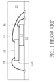
- FIG. 1 One stacked multichip package is generally illustrated in FIG. 1 .
- a first die 11 is mounted on a substrate 10.
- a second die 12 may then be adhesively secured to the top surface of the first die 11 thereby creating a stacked die configuration.
- the second die 12 partially overlaps with the first die 11 when viewed from the above.
- Bonding wires 16 and 18 are then used to electrically connect the first die 11 and the second die 12 to the respective bond fingers on the substrate 10 using conventional wire bonder.
- An encapsulant material 20 is molded over the substrate 10 to provide an encapsulant cap.
- the present invention aims at providing an improved semiconductor package and a fabrication method thereof in order to solve the above-mentioned prior art problems.
- the semiconductor package includes a first semiconductor die having an active surface and a bottom surface opposite to the active surface; a plurality of bond pads distributed on the active surface of the first semiconductor die; an encapsulant covering the active surface of the first semiconductor die, wherein the encapsulant comprises a bottom surface that is flush with the bottom surface of the semiconductor; and a plurality of printed interconnect features embedded in the encapsulant for electrically connecting the plurality of bond pads.
- Each of the printed interconnect features comprises a conductive wire and a conductive pad being integral with the conductive wire.
- the conductive pad is disposed around the first semiconductor die on the bottom surface of the encapsulant.
- the conductive pad has an exposed bottom surface that is flush with the bottom surface of the encapsulant.
- the conductive wire and the conductive pad are integrally formed by using a three-dimensional (3D) printer.
- the printed interconnect features comprise silver, gold, copper, carbon nanotube, graphine, or nano metal particles.
- the semiconductor package further includes a second semiconductor die adhesively secured to the top surface of the first semiconductor die.
- the second semiconductor die partially overlaps with the first semiconductor die when viewed from the above.
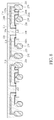
- FIG. 2 is a schematic, cross-sectional diagram showing an exemplary semiconductor package in accordance with one embodiment of the invention.
- semiconductor package 1 comprises a semiconductor die 110.
- the semiconductor die 110 has a top surface or active surface 110a and a bottom surface 110b that is opposite to the active surface 110a.
- a plurality of bond pads or input/output (I/O) pads 121 are distributed on the active surface 110a.
- the active surface 110a, the I/O pads 121, and four side surfaces between the active surface 110a and the bottom surface 110b are covered with an encapsulant 200 such as a molding compound.
- the encapsulant 200 may be formed of an epoxy, a resin, a moldable polymer, or the like.
- the encapsulant 200 may be applied while substantially liquid, and then may be cured through a chemical reaction, such as in an epoxy or resin.
- the molding compound may be an ultraviolet (UV) or thermally cured polymer applied as a gel or malleable solid capable of being disposed around the semiconductor die 110, and then may be cured through a UV or thermal curing process.
- the encapsulant 200 may be cured with a mold (not shown).
- the bottom surface 110b is exposed from a bottom surface 200b of the encapsulant 200.
- the encapsulant 200 has a top surface 200a that is opposite to the bottom surface 200b.
- the exposed bottom surface 110b of the semiconductor die 110 is flush with the bottom surface 200b of the encapsulant 200.
- no re-distribution layer (RDL) is required on the active surface 110a of the semiconductor die 110.
- the semiconductor die 110 may comprise a semiconductor substrate such as a silicon substrate. On the main surface of the semiconductor substrate, a plurality of circuit elements such as transistors may be formed. A plurality of inter-layer dielectric (ILD) layers may be deposited on the semiconductor substrate.
- the ILD layer may be formed of organic materials, which include a polymer base material, non-organic materials, which include silicon nitride (SiN X ), silicon oxide (SiO X ), graphene, or the like.
- a plurality of metal interconnection layers may be formed within the ILD layers.
- the I/O pads 121 of the semiconductor die 110 may be formed in the topmost metal layer covered with a passivation layer, but not limited thereto.
- a plurality of conductive pads 216 and 218 are distributed on the bottom surface 200b of the encapsulant 200.
- the conductive pads 216 and 218 are arranged around the semiconductor die 110 and are electrically connected to the I/O pads 121 on the active surface 110a through the conductive wires 116 and 118 respectively.
- a plurality of connecting elements 230 such as conductive bumps (e.g. C4 bumps or copper pillars) or conductive balls (e.g. BGA balls) may be formed on the conductive pads 216 and 218 for further connection.
- the conductive wires 116 and 118 are integrally formed with the conductive pads 216 and 218.
- the conductive wires 116 and 118 and the conductive pads 216 and 218 may be formed by using a three-dimensional (3D) printer or a wire bonding tool having 3D printing function.
- the conductive wires 116 and 118 and the conductive pads 216 and 218 are encapsulated by the encapsulant 200.
- no packaging substrate or interposer is required.
- the conductive wires 116 and 118 are formed by using a 3D printer or a wire bonding tool having 3D printing function, the conductive wires 116 and 118 may comprise a portion that is bent at right angles, which may avoid shorting of the adjacent wires.
- the semiconductor package 1 may further comprise a passive device 210 such as a discrete capacitor device, a resistor device, an inductor device, or the like.
- the passive device 210 may be disposed adjacent to the bottom surface 200b of the encapsulant 200.
- the passive device 210 may have two terminals 210a and 210b that are electrically connected to the conductive wire 116a and the conductive wire 118a, respectively.
- the conductive wire 116a and the conductive wire 118a are integrally formed with the conductive wires 116 and 118, respectively. Therefore, the terminal 210a is electrically connected to the conductive pad 216 and the semiconductor die 110 through the integral conductive wires 116 and 116a, and the terminal 210b is electrically connected to the conductive pad 218 and the semiconductor die 110 through the integral conductive wires 118 and 118a.
- the conductive wire 116 or 118 may have an integral portion with different patterns, diameters, or structural features formed along the lengthwise direction of the conductive wire 116 or 118.
- FIG. 2 illustrates that the conductive wire 118 may have a widened portion 118b, which is disposed adjacent to the top surface 200a of the encapsulant 200.
- the widened portion 118b may comprise a pad, a plate, a grid, but not limited thereto.
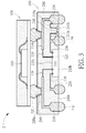
- FIG. 3 is a schematic, cross-sectional diagram showing an exemplary semiconductor package in accordance with another embodiment of the invention, wherein like numeral numbers designate like regions, layers, or elements.
- the semiconductor package 2 may be a package-on-package (PoP).
- the semiconductor package 2 comprises a bottom die package 100 having the structural features as described in FIG. 2 .
- the bottom die package 100 is different from the semiconductor package 1 of FIG. 2 in that openings 260 such as laser-drilled openings are formed in the top surface 200a of the encapsulant 200.
- Each of the openings 260 may expose a portion of the integral portion 118b, which in this embodiment may function as an integral bond pad.
- Conductive elements 320 including, but not limited to, under bump metals and bumps are formed within the openings 260 and on the exposed integral portion 118b.
- a top die package 300 comprising a molded integrated circuit die 310 is mounted on the conductive elements 320.
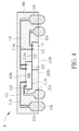
- FIG. 4 is a schematic, cross-sectional diagram showing an exemplary semiconductor package in accordance with still another embodiment of the invention, wherein like numeral numbers designate like regions, layers, or elements.
- the semiconductor package 3 may be a multi-die package.
- the semiconductor package 3 may comprise a lower semiconductor die 110 and an upper semiconductor die 410 that is directly stacked on the lower semiconductor die 110.
- the upper semiconductor die 410 may be adhesively secured to the top surface of the lower semiconductor die 110.
- a plurality of bond pads or I/O pads 121 are distributed on an active surface 110a of the lower semiconductor die 110 and a plurality of bond pads or I/O pads 421 are distributed on an active surface 410a of the upper semiconductor die 410.
- the upper semiconductor die 410 partially overlaps with the lower semiconductor die 110 when viewed from the above. Therefore, the upper semiconductor die 410 comprises an overhanging side edge 412. The overhanging side edge 412 and a bottom surface 410b beyond an edge of the lower semiconductor die 110 are encapsulated by the encapsulant 200.
- a plurality of conductive pads 216 and 218 may be distributed on the bottom surface 200b of the encapsulant 200.
- the conductive pads 216 and 218 may be arranged in an array around the semiconductor die 110 and may be electrically connected to the I/O pads 121 on the active surface 110a and I/O pads 421 on the active surface 410a through the conductive wires 116 and 118 respectively.
- a plurality of connecting elements 230 such as conductive bumps (e.g. C4 bumps or copper pillars) or conductive balls (e.g. BGA balls) may be formed on the conductive pads 216 and 218 for further connection.
- at least an I/O pad 421 is interconnected to at least an I/O pad 121 through the conductive wire 118 and a branched conductive wire 118a, for example, which is integrally formed with the conductive wire 118.
- FIG. 5 to FIG. 9 are schematic, cross-sectional diagrams showing an exemplary method for fabricating the semiconductor package 1 as set forth in FIG. 2 according to one embodiment of the invention.
- a carrier 500 may be provided.
- the carrier 500 may comprise glass, silicon, metal, or any suitable materials.
- a plurality of semiconductor dice 110 is disposed on the carrier 500.
- Each of the semiconductor dice 110 has a top surface or active surface 110a and a bottom surface 110b that is opposite to the active surface 110a.
- a plurality of bond pads or I/O pads 121 are distributed on the active surface 110a.
- the semiconductor dice 110 may be adhesively secured to the top surface of the carrier 500.
- passive devices 210 such as a discrete capacitor device, a resistor device, an inductor device, or the like, may also be disposed on the carrier 500.
- interconnect features 510 including, but not limited to, conductive pads 216 and 218 and conductive wires 116 and 118, are formed on the carrier 500 and on the top surfaces 110a of the semiconductor dice 110.
- the conductive wires 116 and 118 are integrally formed with the conductive pads 216 and 218, respectively.
- the passive device 210 may have two terminals 210a and 210b that are electrically connected to the conductive wire 116a and the conductive wire 118a, respectively.
- the conductive wires 116 and 118 and the conductive pads 216 and 218 may be formed by using a 3D printer or a wire bonding tool having 3D printing function.
- the interconnect features 510 may be composed of silver, gold, copper, carbon nanotube, graphine, or nano metal particles, but not limited thereto. After the formation of the interconnect features 510, optionally, a curing process or a drying process may be performed to cure the interconnect features 510 and/or remove solvent from the interconnect features 510.
- the conductive wire 118 may have an integral portion with different patterns, diameters, or structural features formed along its lengthwise direction.
- the conductive wire 118 may have a widened portion 118b.
- the widened portion 118b may comprise a pad, a plate, a grid, but not limited thereto. It is understood that other features, for example, a heat pipe (not shown), may also be printed on the carrier 500 at this stage.
- the top surface of the carrier 500, the top surfaces 110a of the semiconductor dice 110, the conductive wires 116 and 118, and the conductive pads 216 and 218 are encapsulated by the encapsulant 200.
- the encapsulant 200 may comprise a molding compound including, but not limited to, an epoxy or resin.
- the carrier 500 is then removed to expose the bottom surface 200b of the encapsulant 200, the bottom surfaces 110b of the semiconductor dice 110, and the conductive pads 216 and 218.
- a plurality of connecting elements 230 such as conductive bumps (e.g. C4 bumps or copper pillars) or conductive balls (e.g. BGA balls) may be formed on the conductive pads 216 and 218 for further connection.
- a passivation layer may be formed on the bottom surface 200b of the encapsulant 200 and bottom surfaces 110b of the semiconductor dice 110.
- a dicing process is performed to singulate individual semiconductor packages 1 from one another.
- a dicing tape (not shown) may be used to provide temporary support.
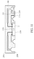
- FIG. 10 to FIG. 12 are schematic, cross-sectional diagrams showing an exemplary method for fabricating the semiconductor package 1 according to another embodiment of the invention, wherein like numeral numbers designate like regions, layers, or elements.
- a temporary interconnect features 510' may be formed by using a 3D printer.
- the temporary interconnect features 510' may be composed of a non-conductive material or an ashable material. For the sake of simplicity, only one semiconductor die 110 on the carrier 500 is shown.
- the top surface of the carrier 500, the top surface 110a of the semiconductor die 110, and the temporary interconnect features 510' are encapsulated by the encapsulant 200.
- the encapsulant 200 may comprise an epoxy molding compound.
- the carrier 500 is then removed to expose the bottom surface 200b of the encapsulant 200, the bottom surfaces 110b of the semiconductor dice 110, and a portion of the temporary interconnect features 510'. Subsequently, the temporary interconnect features 510' is completely removed, thereby forming cavity 530 within the encapsulant 200.
- the cavity 530 is then filled up with conductive material to form interconnect features 510 including, but not limited to, conductive pads 216 and 218 and conductive wires 116 and 118.
- the conductive wires 116 and 118 are integrally formed with the conductive pads 216 and 218.
- the passive device 210 may have two terminals 210a and 210b that are electrically connected to the conductive wire 116a and the conductive wire 118a, respectively.
- the interconnect features 510 may be composed of silver, gold, copper, carbon nanotube, graphine, nano metal particles, or solder, but not limited thereto. After the formation of the interconnect features 510, optionally, a curing process, a reflow process, or a drying process may be performed.
- FIG. 13 is a schematic perspective diagram showing an exemplary semiconductor package in accordance with still another embodiment of the invention, wherein like numeral numbers designate like regions, layers, or elements.
- the semiconductor package 4 may be a multi-die package.
- the semiconductor package 4 may comprise a substrate 101 having a top surface 101a and a bottom surface 101b that is opposite to the top surface 101a.
- the substrate 101 may comprise a packaging substrate or a printed wiring board, but not limited thereto.
- a plurality of bond fingers 102 may be arranged on the top surface 101 a of the substrate 101 along its perimeter.
- a plurality of solder balls 103 may be arranged on the bottom surface 101b.
- the semiconductor package 4 may comprise a lower semiconductor die 110 and an upper semiconductor die 410 that is directly stacked on the lower semiconductor die 110.
- the upper semiconductor die 410 may be adhesively secured to the top surface 110a of the lower semiconductor die 110.
- a plurality of bond pads or I/O pads 121 are distributed on an active surface 110a of the lower semiconductor die 110 and a plurality of bond pads or I/O pads 421 are distributed on an active surface 410a of the upper semiconductor die 410.
- the upper semiconductor die 410 partially overlaps with the lower semiconductor die 110 when viewed from the above. Therefore, the upper semiconductor die 410 comprises an overhanging side edge 412.
- the overhanging side edge 412 and a bottom surface 410b beyond an edge of the lower semiconductor die 110 may be encapsulated by the encapsulant (not shown).
- 3D printed features 600 including, but not limited to, conductive wires 610, PMU (power management unit) heatpipe 620, inductor 630, and power bar 640, may be formed on the top surface 410a of the upper semiconductor die 410 and on the top surface 110a of the lower semiconductor die 110.
- the conductive wires 610 may interconnect the bond pads 421, the bond pads 121, and/or the bond fingers 102.
- one conductive wire 610 may be electrically connected to multiple bond fingers 102 through the sub-wires 610a that is formed integrally with the conductive wire 610.
Landscapes
- Engineering & Computer Science (AREA)
- Manufacturing & Machinery (AREA)
- Structures Or Materials For Encapsulating Or Coating Semiconductor Devices Or Solid State Devices (AREA)
Abstract
Description
- The present invention relates to interconnects of integrated circuits and semiconductor packages.
- An integrated circuit (IC) die is a small device formed on a semiconductor wafer, such as a silicon wafer. Such a die is typically cut from the wafer and attached to a substrate for interconnect redistribution. Bond pads on the die are then electrically connected to the leads on the carrier via wire bonding. The die and wire bonds are then encapsulated with a molding compound such that a package is formed.
- Typically, the leads encapsulated in the package are redistributed in a network of conductors within the carrier and end in an array of terminal points outside the package. Manufacturers have been stacking two or more die within a single package. Such devices are sometimes referred to as stacked multichip packages.
- One stacked multichip package is generally illustrated in
FIG. 1 . In this configuration afirst die 11 is mounted on asubstrate 10. Asecond die 12 may then be adhesively secured to the top surface of thefirst die 11 thereby creating a stacked die configuration. Thesecond die 12 partially overlaps with thefirst die 11 when viewed from the above.Bonding wires first die 11 and thesecond die 12 to the respective bond fingers on thesubstrate 10 using conventional wire bonder. Anencapsulant material 20 is molded over thesubstrate 10 to provide an encapsulant cap. - However, it is difficult to form the
wire bond 18 on the bond pads of thesecond die 12 adjacent to the overhangingside edge 12a. The stress incurred by the wire bonder may cause peeling between thefirst die 11 and thesecond die 12 and reduce the production yield. - This in mind, the present invention aims at providing an improved semiconductor package and a fabrication method thereof in order to solve the above-mentioned prior art problems.
- This is achieved by a semiconductor package according to the pre-characterizing clause of
claim 1. The dependent claims pertain to corresponding further developments and improvements. - As will be seen more clearly from the detailed description following below, the semiconductor package includes a first semiconductor die having an active surface and a bottom surface opposite to the active surface; a plurality of bond pads distributed on the active surface of the first semiconductor die; an encapsulant covering the active surface of the first semiconductor die, wherein the encapsulant comprises a bottom surface that is flush with the bottom surface of the semiconductor; and a plurality of printed interconnect features embedded in the encapsulant for electrically connecting the plurality of bond pads. Each of the printed interconnect features comprises a conductive wire and a conductive pad being integral with the conductive wire.
- According to one embodiment, the conductive pad is disposed around the first semiconductor die on the bottom surface of the encapsulant. The conductive pad has an exposed bottom surface that is flush with the bottom surface of the encapsulant.
- According to one embodiment, the conductive wire and the conductive pad are integrally formed by using a three-dimensional (3D) printer. The printed interconnect features comprise silver, gold, copper, carbon nanotube, graphine, or nano metal particles.
- According to another embodiment, the semiconductor package further includes a second semiconductor die adhesively secured to the top surface of the first semiconductor die. The second semiconductor die partially overlaps with the first semiconductor die when viewed from the above.
- These and other objectives of the present invention will no doubt become obvious to those of ordinary skill in the art after reading the following detailed description of the preferred embodiment that is illustrated in the various figures and drawings.
- The accompanying drawings are included to provide a further understanding of the invention, and are incorporated in and constitute a part of this specification. The drawings illustrate embodiments of the invention and, together with the description, serve to explain the principles of the invention. In the drawings:
-
FIG. 1 is a schematic, cross-sectional diagram showing a conventional stacked multichip package; -
FIG. 2 is a schematic, cross-sectional diagram showing an exemplary semiconductor package in accordance with one embodiment of the invention; -
FIG. 3 is a schematic, cross-sectional diagram showing an exemplary package-on-package (PoP) in accordance with another embodiment of the invention; -
FIG. 4 is a schematic, cross-sectional diagram showing an exemplary multi-die package in accordance with still another embodiment of the invention; -
FIG. 5 to FIG. 9 are schematic, cross-sectional diagrams showing an exemplary method for fabricating the semiconductor package as set forth inFIG. 2 according to one embodiment of the invention; -
FIG. 10 to FIG. 12 are schematic, cross-sectional diagrams showing an exemplary method for fabricating the semiconductor package as set forth inFIG. 2 according to another embodiment of the invention; and -
FIG. 13 is a schematic perspective diagram showing an exemplary semiconductor package in accordance with still another embodiment of the invention. - In the following detailed description of embodiments of the invention, reference is made to the accompanying drawings, which form a part hereof, and in which is shown by way of illustration specific preferred embodiments in which the disclosure may be practiced.
- These embodiments are described in sufficient detail to enable those skilled in the art to practice them, and it is to be understood that other embodiments may be utilized and that mechanical, chemical, electrical, and procedural changes may be made without departing from the spirit and scope of the present disclosure. The following detailed description is, therefore, not to be taken in a limiting sense, and the scope of embodiments of the present invention is defined only by the appended claims.
- Please refer to
FIG. 2. FIG. 2 is a schematic, cross-sectional diagram showing an exemplary semiconductor package in accordance with one embodiment of the invention. As shown inFIG. 2 ,semiconductor package 1 comprises asemiconductor die 110. Thesemiconductor die 110 has a top surface oractive surface 110a and abottom surface 110b that is opposite to theactive surface 110a. A plurality of bond pads or input/output (I/O)pads 121 are distributed on theactive surface 110a. According to the embodiment of the invention, theactive surface 110a, the I/O pads 121, and four side surfaces between theactive surface 110a and thebottom surface 110b are covered with anencapsulant 200 such as a molding compound. - In some embodiments, the encapsulant 200 may be formed of an epoxy, a resin, a moldable polymer, or the like. The
encapsulant 200 may be applied while substantially liquid, and then may be cured through a chemical reaction, such as in an epoxy or resin. In some other embodiments, the molding compound may be an ultraviolet (UV) or thermally cured polymer applied as a gel or malleable solid capable of being disposed around thesemiconductor die 110, and then may be cured through a UV or thermal curing process. Theencapsulant 200 may be cured with a mold (not shown). - According to the embodiment of the invention, the
bottom surface 110b is exposed from abottom surface 200b of theencapsulant 200. Theencapsulant 200 has atop surface 200a that is opposite to thebottom surface 200b. According to the embodiment of the invention, the exposedbottom surface 110b of thesemiconductor die 110 is flush with thebottom surface 200b of theencapsulant 200. According to the embodiment of the invention, no re-distribution layer (RDL) is required on theactive surface 110a of thesemiconductor die 110. - For the sake of simplicity, the structural details within the
semiconductor die 110 are not shown in this figure. It is understood that thesemiconductor die 110 may comprise a semiconductor substrate such as a silicon substrate. On the main surface of the semiconductor substrate, a plurality of circuit elements such as transistors may be formed. A plurality of inter-layer dielectric (ILD) layers may be deposited on the semiconductor substrate. The ILD layer may be formed of organic materials, which include a polymer base material, non-organic materials, which include silicon nitride (SiNX), silicon oxide (SiOX), graphene, or the like. A plurality of metal interconnection layers may be formed within the ILD layers. The I/O pads 121 of the semiconductor die 110 may be formed in the topmost metal layer covered with a passivation layer, but not limited thereto. - A plurality of
conductive pads bottom surface 200b of theencapsulant 200. Theconductive pads O pads 121 on theactive surface 110a through theconductive wires elements 230 such as conductive bumps (e.g. C4 bumps or copper pillars) or conductive balls (e.g. BGA balls) may be formed on theconductive pads - It is one germane feature of the embodiment of the invention that the
conductive wires conductive pads conductive wires conductive pads conductive wires conductive pads encapsulant 200. According to the embodiment of the invention, no packaging substrate or interposer is required. Further, since theconductive wires conductive wires - According to the embodiment of the invention, the
semiconductor package 1 may further comprise apassive device 210 such as a discrete capacitor device, a resistor device, an inductor device, or the like. Thepassive device 210 may be disposed adjacent to thebottom surface 200b of theencapsulant 200. According to the embodiment of the invention, thepassive device 210 may have twoterminals conductive wire 116a and theconductive wire 118a, respectively. - According to the embodiment of the invention, the
conductive wire 116a and theconductive wire 118a are integrally formed with theconductive wires conductive pad 216 and the semiconductor die 110 through the integralconductive wires conductive pad 218 and the semiconductor die 110 through the integralconductive wires - According to the embodiment of the invention, the
conductive wire conductive wire FIG. 2 illustrates that theconductive wire 118 may have a widenedportion 118b, which is disposed adjacent to thetop surface 200a of theencapsulant 200. The widenedportion 118b may comprise a pad, a plate, a grid, but not limited thereto. - Please refer to
FIG. 3. FIG. 3 is a schematic, cross-sectional diagram showing an exemplary semiconductor package in accordance with another embodiment of the invention, wherein like numeral numbers designate like regions, layers, or elements. As shown inFIG. 3 , thesemiconductor package 2 may be a package-on-package (PoP). Thesemiconductor package 2 comprises abottom die package 100 having the structural features as described inFIG. 2 . The bottom diepackage 100 is different from thesemiconductor package 1 ofFIG. 2 in thatopenings 260 such as laser-drilled openings are formed in thetop surface 200a of theencapsulant 200. - Each of the
openings 260 may expose a portion of theintegral portion 118b, which in this embodiment may function as an integral bond pad.Conductive elements 320 including, but not limited to, under bump metals and bumps are formed within theopenings 260 and on the exposedintegral portion 118b. Atop die package 300 comprising a molded integrated circuit die 310 is mounted on theconductive elements 320. - Please refer to
FIG. 4. FIG. 4 is a schematic, cross-sectional diagram showing an exemplary semiconductor package in accordance with still another embodiment of the invention, wherein like numeral numbers designate like regions, layers, or elements. As shown inFIG. 4 , thesemiconductor package 3 may be a multi-die package. Thesemiconductor package 3 may comprise a lower semiconductor die 110 and an upper semiconductor die 410 that is directly stacked on the lower semiconductor die 110. The upper semiconductor die 410 may be adhesively secured to the top surface of the lower semiconductor die 110. A plurality of bond pads or I/O pads 121 are distributed on anactive surface 110a of the lower semiconductor die 110 and a plurality of bond pads or I/O pads 421 are distributed on anactive surface 410a of the upper semiconductor die 410. - According to the embodiment of the invention, the upper semiconductor die 410 partially overlaps with the lower semiconductor die 110 when viewed from the above. Therefore, the upper semiconductor die 410 comprises an overhanging
side edge 412. The overhangingside edge 412 and abottom surface 410b beyond an edge of the lower semiconductor die 110 are encapsulated by theencapsulant 200. - Likewise, a plurality of
conductive pads bottom surface 200b of theencapsulant 200. Theconductive pads O pads 121 on theactive surface 110a and I/O pads 421 on theactive surface 410a through theconductive wires - A plurality of connecting
elements 230 such as conductive bumps (e.g. C4 bumps or copper pillars) or conductive balls (e.g. BGA balls) may be formed on theconductive pads O pad 421 is interconnected to at least an I/O pad 121 through theconductive wire 118 and a branchedconductive wire 118a, for example, which is integrally formed with theconductive wire 118. -
FIG. 5 to FIG. 9 are schematic, cross-sectional diagrams showing an exemplary method for fabricating thesemiconductor package 1 as set forth inFIG. 2 according to one embodiment of the invention. As shown inFIG. 5 , first, acarrier 500 may be provided. Thecarrier 500 may comprise glass, silicon, metal, or any suitable materials. A plurality ofsemiconductor dice 110 is disposed on thecarrier 500. Each of thesemiconductor dice 110 has a top surface oractive surface 110a and abottom surface 110b that is opposite to theactive surface 110a. A plurality of bond pads or I/O pads 121 are distributed on theactive surface 110a. - The
semiconductor dice 110 may be adhesively secured to the top surface of thecarrier 500. Optionally,passive devices 210, such as a discrete capacitor device, a resistor device, an inductor device, or the like, may also be disposed on thecarrier 500. - As shown in
FIG. 6 , interconnect features 510 including, but not limited to,conductive pads conductive wires carrier 500 and on thetop surfaces 110a of thesemiconductor dice 110. Theconductive wires conductive pads passive device 210 may have twoterminals conductive wire 116a and theconductive wire 118a, respectively. - For example, the
conductive wires conductive pads - According to the embodiment of the invention, for example, the
conductive wire 118 may have an integral portion with different patterns, diameters, or structural features formed along its lengthwise direction. For example, theconductive wire 118 may have a widenedportion 118b. The widenedportion 118b may comprise a pad, a plate, a grid, but not limited thereto. It is understood that other features, for example, a heat pipe (not shown), may also be printed on thecarrier 500 at this stage. - As shown in
FIG. 7 , subsequently, the top surface of thecarrier 500, thetop surfaces 110a of thesemiconductor dice 110, theconductive wires conductive pads encapsulant 200. For example, theencapsulant 200 may comprise a molding compound including, but not limited to, an epoxy or resin. - As shown in
FIG. 8 , thecarrier 500 is then removed to expose thebottom surface 200b of theencapsulant 200, the bottom surfaces 110b of thesemiconductor dice 110, and theconductive pads elements 230 such as conductive bumps (e.g. C4 bumps or copper pillars) or conductive balls (e.g. BGA balls) may be formed on theconductive pads bottom surface 200b of theencapsulant 200 andbottom surfaces 110b of thesemiconductor dice 110. - As shown in
FIG. 9 , after the formation of the connectingelements 230, a dicing process is performed to singulateindividual semiconductor packages 1 from one another. During the aforesaid dicing process, a dicing tape (not shown) may be used to provide temporary support. -
FIG. 10 to FIG. 12 are schematic, cross-sectional diagrams showing an exemplary method for fabricating thesemiconductor package 1 according to another embodiment of the invention, wherein like numeral numbers designate like regions, layers, or elements. - As shown in
FIG. 10 , after mounting the semiconductor die 110 and thepassive device 210 on thecarrier 500, a temporary interconnect features 510' may be formed by using a 3D printer. According to the embodiment of the invention, the temporary interconnect features 510' may be composed of a non-conductive material or an ashable material. For the sake of simplicity, only one semiconductor die 110 on thecarrier 500 is shown. - Subsequently, the top surface of the
carrier 500, thetop surface 110a of the semiconductor die 110, and the temporary interconnect features 510' are encapsulated by theencapsulant 200. For example, theencapsulant 200 may comprise an epoxy molding compound. - As shown in
FIG. 11 , thecarrier 500 is then removed to expose thebottom surface 200b of theencapsulant 200, the bottom surfaces 110b of thesemiconductor dice 110, and a portion of the temporary interconnect features 510'. Subsequently, the temporary interconnect features 510' is completely removed, thereby formingcavity 530 within theencapsulant 200. - As shown in
FIG. 12 , thecavity 530 is then filled up with conductive material to form interconnect features 510 including, but not limited to,conductive pads conductive wires conductive wires conductive pads passive device 210 may have twoterminals conductive wire 116a and theconductive wire 118a, respectively. - For example, the interconnect features 510 may be composed of silver, gold, copper, carbon nanotube, graphine, nano metal particles, or solder, but not limited thereto. After the formation of the interconnect features 510, optionally, a curing process, a reflow process, or a drying process may be performed.
-
FIG. 13 is a schematic perspective diagram showing an exemplary semiconductor package in accordance with still another embodiment of the invention, wherein like numeral numbers designate like regions, layers, or elements. As shown inFIG. 13 , thesemiconductor package 4 may be a multi-die package. Thesemiconductor package 4 may comprise asubstrate 101 having atop surface 101a and abottom surface 101b that is opposite to thetop surface 101a. Thesubstrate 101 may comprise a packaging substrate or a printed wiring board, but not limited thereto. A plurality ofbond fingers 102 may be arranged on thetop surface 101 a of thesubstrate 101 along its perimeter. On thebottom surface 101b, a plurality ofsolder balls 103 may be arranged. - The
semiconductor package 4 may comprise a lower semiconductor die 110 and an upper semiconductor die 410 that is directly stacked on the lower semiconductor die 110. The upper semiconductor die 410 may be adhesively secured to thetop surface 110a of the lower semiconductor die 110. A plurality of bond pads or I/O pads 121 are distributed on anactive surface 110a of the lower semiconductor die 110 and a plurality of bond pads or I/O pads 421 are distributed on anactive surface 410a of the upper semiconductor die 410. According to the embodiment of the invention, the upper semiconductor die 410 partially overlaps with the lower semiconductor die 110 when viewed from the above. Therefore, the upper semiconductor die 410 comprises an overhangingside edge 412. The overhangingside edge 412 and abottom surface 410b beyond an edge of the lower semiconductor die 110 may be encapsulated by the encapsulant (not shown). - According to the embodiment of the invention, 3D printed
features 600 including, but not limited to,conductive wires 610, PMU (power management unit)heatpipe 620,inductor 630, andpower bar 640, may be formed on thetop surface 410a of the upper semiconductor die 410 and on thetop surface 110a of the lower semiconductor die 110. According to the embodiment of the invention, theconductive wires 610 may interconnect thebond pads 421, thebond pads 121, and/or thebond fingers 102. For example, oneconductive wire 610 may be electrically connected tomultiple bond fingers 102 through the sub-wires 610a that is formed integrally with theconductive wire 610.
Claims (15)
- A semiconductor package (1, 2, 3, 4), characterized by:a first semiconductor die (110) having an active surface (110a) and a bottom surface (110b) opposite to the active surface (110a);a plurality of input/output (I/O) pads (121) distributed on the active surface (110a) of the first semiconductor die (110);an encapsulant (200) covering the active surface (110a) of the first semiconductor die (110), wherein the encapsulant (200) comprises a bottom surface (200b) that is flush with the bottom surface (110b) of the first semiconductor die (110); anda plurality of printed interconnect features (510) embedded in the encapsulant (200) for electrically connecting the plurality of I/O pads (121), wherein each of the printed interconnect features (510) comprises a conductive wire (116, 118) and a conductive pad (216, 218) being integral with the conductive wire (116, 118).
- The semiconductor package (1, 2, 3, 4) according to claim 1, further characterized in that the conductive pad (216, 218) is disposed around the first semiconductor die (110) on the bottom surface (200b) of the encapsulant (200), and wherein the conductive pad (216, 218) has an exposed bottom surface that is flush with the bottom surface (200b) of the encapsulant (200).
- The semiconductor package (1, 2, 3, 4) according to claim 1, further characterized in that the conductive wire (116, 118) and the conductive pad (216, 218) are integrally formed by using a three-dimensional (3D) printer.
- The semiconductor package (1, 2, 3, 4) according to claim 1, further characterized in that the printed interconnect features (510) comprise silver, gold, copper, carbon nanotube, graphine, or nano metal particles.
- The semiconductor package (1, 2, 3, 4) according to claim 1, further characterized in that the encapsulant (200) comprises an epoxy, a resin, or a moldable polymer.
- The semiconductor package (1, 2, 3, 4) according to claim 1, further characterized in that the bottom surface (110b) of the first semiconductor die (110) is not covered by the encapsulant (200).
- The semiconductor package (1, 2, 3, 4) according to claim 1, further characterized in that the conductive wire (118) comprises a widened portion (118b) disposed adjacent to a top surface (200a) of the encapsulant (200).
- The semiconductor package (1, 2, 3, 4) according to claim 7, further characterized in that the widened portion (118b) comprises a pad.
- The semiconductor package (1, 2, 3, 4) according to claim 8, further characterized in that an opening (260) is formed in the top surface (200a) of the encapsulant (200) to expose the pad.
- The semiconductor package (1, 2, 3, 4) according to claim 9, further characterized in that a conductive element (320) is disposed in the opening (260) and on the pad.
- The semiconductor package (1, 2, 3, 4) according to claim 10, further characterized in that a die package (300) is mounted on the top surface (200a) of the encapsulant (200) and is electrically connected to the conductive element (320).
- The semiconductor package (1, 2, 3, 4) according to claim 1, further characterized in that a passive device (210) is embedded in the encapsulant (200) and electrically connected to the printed interconnect features (510).
- The semiconductor package (1, 2, 3, 4) according to claim 1, further characterized in that a second semiconductor die (410) is adhesively secured to the top surface (110a) of the first semiconductor die (110).
- The semiconductor package (1, 2, 3, 4) according to claim 13, further characterized in that the second semiconductor die (410) partially overlaps with the first semiconductor die (110) when viewed from above.
- The semiconductor package (1, 2, 3, 4) according to claim 1, further characterized in that the conductive wire (116, 118) comprises a portion bent at right angles.
Applications Claiming Priority (3)
| Application Number | Priority Date | Filing Date | Title |
|---|---|---|---|
| US201562161591P | 2015-05-14 | 2015-05-14 | |
| US201562190401P | 2015-07-09 | 2015-07-09 | |
| US15/063,433 US9842831B2 (en) | 2015-05-14 | 2016-03-07 | Semiconductor package and fabrication method thereof |
Publications (3)
| Publication Number | Publication Date |
|---|---|
| EP3093877A2 true EP3093877A2 (en) | 2016-11-16 |
| EP3093877A3 EP3093877A3 (en) | 2017-02-22 |
| EP3093877B1 EP3093877B1 (en) | 2019-07-24 |
Family
ID=55589710
Family Applications (1)
| Application Number | Title | Priority Date | Filing Date |
|---|---|---|---|
| EP16161578.6A Active EP3093877B1 (en) | 2015-05-14 | 2016-03-22 | Semiconductor package |
Country Status (4)
| Country | Link |
|---|---|
| US (2) | US9842831B2 (en) |
| EP (1) | EP3093877B1 (en) |
| CN (1) | CN106158818B (en) |
| TW (1) | TWI575624B (en) |
Cited By (1)
| Publication number | Priority date | Publication date | Assignee | Title |
|---|---|---|---|---|
| CN109313189A (en) * | 2016-06-15 | 2019-02-05 | 纳米医学工程诊断学公司 | Patterning Graphene with Hardmask Coatings |
Families Citing this family (20)
| Publication number | Priority date | Publication date | Assignee | Title |
|---|---|---|---|---|
| KR102353254B1 (en) | 2014-08-07 | 2022-01-18 | 오르보테크 엘티디. | Lift printing system |
| WO2016063270A1 (en) | 2014-10-19 | 2016-04-28 | Orbotech Ltd. | Llift printing of conductive traces onto a semiconductor substrate |
| EP3247816A4 (en) | 2015-01-19 | 2018-01-24 | Orbotech Ltd. | Printing of three-dimensional metal structures with a sacrificial support |
| JP2016192447A (en) * | 2015-03-30 | 2016-11-10 | 株式会社東芝 | Semiconductor device |
| US9842831B2 (en) | 2015-05-14 | 2017-12-12 | Mediatek Inc. | Semiconductor package and fabrication method thereof |
| US10685943B2 (en) | 2015-05-14 | 2020-06-16 | Mediatek Inc. | Semiconductor chip package with resilient conductive paste post and fabrication method thereof |
| KR20180030609A (en) | 2015-07-09 | 2018-03-23 | 오르보테크 엘티디. | Control of LIFT discharge angle |
| CN108349120B (en) | 2015-11-22 | 2020-06-23 | 奥博泰克有限公司 | Surface Properties Control of Printed 3D Structures |
| DE102016224631B4 (en) * | 2016-12-09 | 2020-06-04 | Fraunhofer-Gesellschaft zur Förderung der angewandten Forschung e.V. | Electrically conductive connection between at least two electrical components on a carrier equipped with electronic and / or electrical components, which is formed with a bonding wire |
| US10971478B2 (en) | 2016-12-30 | 2021-04-06 | Intel Corporation | Interposer design in package structures for wire bonding applications |
| TW201901887A (en) * | 2017-05-24 | 2019-01-01 | 以色列商奧寶科技股份有限公司 | Electrical interconnection circuit components on the substrate without prior patterning |
| US10546817B2 (en) * | 2017-12-28 | 2020-01-28 | Intel IP Corporation | Face-up fan-out electronic package with passive components using a support |
| KR102102389B1 (en) * | 2018-09-18 | 2020-04-21 | 전자부품연구원 | Semiconductor package for high power and high frequency applications and manufacturing method thereof |
| TWI692062B (en) * | 2018-11-01 | 2020-04-21 | 華邦電子股份有限公司 | Circuit structure and method of manufacturing the same |
| TWI677949B (en) | 2018-11-21 | 2019-11-21 | 華邦電子股份有限公司 | Semiconductor device |
| KR102302633B1 (en) * | 2019-08-02 | 2021-09-14 | 동국대학교 경주캠퍼스 산학협력단 | Manufacturing method of super-hydrophobic surface with 3d printer and nanowire |
| CN113307647B (en) * | 2021-04-16 | 2022-05-31 | 长春工业大学 | Indirect brazing method of aluminum nitride ceramic copper-clad plate |
| CN114446838B (en) * | 2022-03-03 | 2025-05-16 | 芯体素(杭州)科技发展有限公司 | Ball implantation method, device, electronic device and storage medium based on 3D printing process |
| US12622280B2 (en) * | 2022-09-08 | 2026-05-05 | Nxp Usa, Inc. | Semiconductor device with through package via and method therefor |
| CN118057965A (en) * | 2022-09-21 | 2024-05-21 | 长江先进存储产业创新中心有限责任公司 | Integrated circuit device, package and method of forming the same |
Family Cites Families (54)
| Publication number | Priority date | Publication date | Assignee | Title |
|---|---|---|---|---|
| JPH0252443A (en) | 1988-08-17 | 1990-02-22 | Mitsubishi Electric Corp | Wire bonding |
| JPH05299530A (en) | 1992-04-17 | 1993-11-12 | Oki Electric Ind Co Ltd | Resin-sealed semiconductor device and manufacturing method thereof |
| JPH08107123A (en) | 1994-10-04 | 1996-04-23 | Hitachi Ltd | Method of manufacturing semiconductor integrated circuit device, manufacturing apparatus thereof, and semiconductor integrated circuit device |
| JP2001230270A (en) | 2000-02-14 | 2001-08-24 | Fujitsu Ltd | Semiconductor device and manufacturing method thereof |
| WO2003084297A1 (en) | 2002-03-28 | 2003-10-09 | Shinko Electric Industries Co., Ltd. | Wiring structure and its manufacturing method |
| US7633765B1 (en) | 2004-03-23 | 2009-12-15 | Amkor Technology, Inc. | Semiconductor package including a top-surface metal layer for implementing circuit features |
| US7176580B1 (en) | 2003-10-24 | 2007-02-13 | Joseph Fjelstad | Structures and methods for wire bonding over active, brittle and low K dielectric areas of an IC chip |
| US7205178B2 (en) | 2004-03-24 | 2007-04-17 | Freescale Semiconductor, Inc. | Land grid array packaged device and method of forming same |
| US9318428B2 (en) | 2004-05-28 | 2016-04-19 | Nxp B.V. | Chip having two groups of chip contacts |
| JP5592055B2 (en) | 2004-11-03 | 2014-09-17 | テッセラ,インコーポレイテッド | Improved stacking packaging |
| US7394148B2 (en) | 2005-06-20 | 2008-07-01 | Stats Chippac Ltd. | Module having stacked chip scale semiconductor packages |
| JP2007123595A (en) | 2005-10-28 | 2007-05-17 | Nec Corp | Semiconductor device and its mounting structure |
| US8344524B2 (en) | 2006-03-07 | 2013-01-01 | Megica Corporation | Wire bonding method for preventing polymer cracking |
| US20070216033A1 (en) | 2006-03-20 | 2007-09-20 | Corisis David J | Carrierless chip package for integrated circuit devices, and methods of making same |
| WO2007107964A1 (en) * | 2006-03-23 | 2007-09-27 | Nxp B.V. | Electrically enhanced wirebond package |
| US7915081B2 (en) * | 2006-03-31 | 2011-03-29 | Intel Corporation | Flexible interconnect pattern on semiconductor package |
| JP5598787B2 (en) | 2006-04-17 | 2014-10-01 | マイクロンメモリジャパン株式会社 | Manufacturing method of stacked semiconductor device |
| TWI395275B (en) | 2006-09-06 | 2013-05-01 | 米輯電子股份有限公司 | Chip package structure and its process |
| EP2130222B1 (en) * | 2007-02-14 | 2018-09-05 | III Holdings 6, LLC | A carrier for bonding a semiconductor chip onto and a method of contacting a semiconductor chip to a carrier |
| JP5123633B2 (en) | 2007-10-10 | 2013-01-23 | ルネサスエレクトロニクス株式会社 | Semiconductor devices and connecting materials |
| US8035211B2 (en) | 2008-03-26 | 2011-10-11 | Stats Chippac Ltd. | Integrated circuit package system with support structure under wire-in-film adhesive |
| JP2010087208A (en) | 2008-09-30 | 2010-04-15 | Fujifilm Corp | Method for forming three-dimensional structure, method for manufacturing semiconductor device, and semiconductor device |
| US7838332B2 (en) * | 2008-11-26 | 2010-11-23 | Infineon Technologies Ag | Method of manufacturing a semiconductor package with a bump using a carrier |
| CN101764113B (en) | 2008-12-25 | 2012-02-29 | 俞宛伶 | Metal bump structure and forming method on connection pad of circuit surface of semiconductor element |
| JPWO2010087336A1 (en) * | 2009-01-27 | 2012-08-02 | パナソニック株式会社 | Semiconductor chip mounting method, semiconductor device obtained by using the method, semiconductor chip connection method, three-dimensional structure provided with wiring on the surface, and manufacturing method thereof |
| US8026589B1 (en) | 2009-02-23 | 2011-09-27 | Amkor Technology, Inc. | Reduced profile stackable semiconductor package |
| KR20100124161A (en) | 2009-05-18 | 2010-11-26 | 주식회사 하이닉스반도체 | Fabricating method for semiconductor package |
| KR101624973B1 (en) * | 2009-09-23 | 2016-05-30 | 삼성전자주식회사 | Package on package type semiconductor package and method for fabricating the same |
| JP2011077460A (en) | 2009-10-02 | 2011-04-14 | Toyota Motor Corp | Semiconductor device, and manufacturing method thereof |
| TW201133655A (en) | 2010-03-22 | 2011-10-01 | Powertech Technology Inc | Packaging method of array-cutting type quad flat non-leaded packages |
| KR101712043B1 (en) | 2010-10-14 | 2017-03-03 | 삼성전자주식회사 | Stacked semiconductor package, Semiconductor device including the stacked semiconductor package and Method of manufacturing the stacked semiconductor package |
| US8492203B2 (en) | 2011-01-21 | 2013-07-23 | Stats Chippac, Ltd. | Semiconductor device and method for forming semiconductor package having build-up interconnect structure over semiconductor die with different CTE insulating layers |
| US20120228768A1 (en) | 2011-03-07 | 2012-09-13 | Reza Argenty Pagaila | Integrated circuit packaging system using b-stage polymer and method of manufacture thereof |
| WO2012126377A1 (en) * | 2011-03-22 | 2012-09-27 | Nantong Fujitsu Microelectronics Co., Ltd. | System-level packaging methods and structures |
| EP2727145A4 (en) * | 2011-07-03 | 2015-07-29 | Eoplex Ltd | DRIVER SUPPORT COMPRISING THERMALLY FUSED HOUSING COMPONENTS |
| US9324659B2 (en) * | 2011-08-01 | 2016-04-26 | Stats Chippac, Ltd. | Semiconductor device and method of forming POP with stacked semiconductor die and bumps formed directly on the lower die |
| US10128161B2 (en) * | 2011-10-27 | 2018-11-13 | Global Circuit Innovations, Inc. | 3D printed hermetic package assembly and method |
| KR20140064053A (en) | 2012-11-19 | 2014-05-28 | 삼성전자주식회사 | Semiconductor package having redistribution layer |
| WO2014037815A2 (en) * | 2012-09-07 | 2014-03-13 | Eoplex Limited | Lead carrier with print-formed terminal pads |
| TWI481901B (en) | 2012-12-03 | 2015-04-21 | Wistron Corp | Head-mounted display |
| WO2014112954A1 (en) * | 2013-01-21 | 2014-07-24 | Pbt Pte. Ltd. | Substrate for semiconductor packaging and method of forming same |
| JP6273945B2 (en) * | 2013-04-26 | 2018-02-07 | 日亜化学工業株式会社 | Light emitting device |
| US9281338B2 (en) | 2014-04-25 | 2016-03-08 | Taiwan Semiconductor Manufacturing Company, Ltd. | Semiconductor image sensor device having back side illuminated image sensors with embedded color filters |
| JP6437246B2 (en) | 2014-08-28 | 2018-12-12 | ルネサスエレクトロニクス株式会社 | Semiconductor device and manufacturing method thereof |
| KR102320046B1 (en) | 2014-09-19 | 2021-11-01 | 삼성전자주식회사 | Semiconductor Packages Having a Cascaded Chip Stack |
| MY199192A (en) | 2014-09-26 | 2023-10-19 | Intel Corp | Integrated circuit package having wire-bonded multi-die stack |
| US9559069B2 (en) | 2015-01-29 | 2017-01-31 | Taiwan Semiconductor Manufacturing Co., Ltd. | Semiconductor device, integrated circuit structure using the same, and manufacturing method thereof |
| US9960130B2 (en) | 2015-02-06 | 2018-05-01 | UTAC Headquarters Pte. Ltd. | Reliable interconnect |
| US20160307873A1 (en) | 2015-04-16 | 2016-10-20 | Mediatek Inc. | Bonding pad arrangment design for semiconductor package |
| US10446522B2 (en) | 2015-04-16 | 2019-10-15 | Taiwan Semiconductor Manufacturing Company, Ltd. | Methods of forming multiple conductive features in semiconductor devices in a same formation process |
| US10685943B2 (en) | 2015-05-14 | 2020-06-16 | Mediatek Inc. | Semiconductor chip package with resilient conductive paste post and fabrication method thereof |
| US9842831B2 (en) | 2015-05-14 | 2017-12-12 | Mediatek Inc. | Semiconductor package and fabrication method thereof |
| CN205303447U (en) | 2015-12-28 | 2016-06-08 | 江阴长电先进封装有限公司 | Packaging structure of fingerprint identification sensor |
| KR102570325B1 (en) | 2016-11-16 | 2023-08-25 | 에스케이하이닉스 주식회사 | Stacked type semiconductor package having redistribution line structure |
-
2016
- 2016-03-07 US US15/063,433 patent/US9842831B2/en active Active
- 2016-03-22 EP EP16161578.6A patent/EP3093877B1/en active Active
- 2016-04-11 CN CN201610221935.1A patent/CN106158818B/en active Active
- 2016-04-18 TW TW105111959A patent/TWI575624B/en not_active IP Right Cessation
-
2017
- 2017-11-06 US US15/805,097 patent/US10340259B2/en active Active
Non-Patent Citations (1)
| Title |
|---|
| None |
Cited By (1)
| Publication number | Priority date | Publication date | Assignee | Title |
|---|---|---|---|---|
| CN109313189A (en) * | 2016-06-15 | 2019-02-05 | 纳米医学工程诊断学公司 | Patterning Graphene with Hardmask Coatings |
Also Published As
| Publication number | Publication date |
|---|---|
| EP3093877B1 (en) | 2019-07-24 |
| TWI575624B (en) | 2017-03-21 |
| US20160336303A1 (en) | 2016-11-17 |
| TW201640599A (en) | 2016-11-16 |
| US20180076185A1 (en) | 2018-03-15 |
| CN106158818B (en) | 2018-11-30 |
| EP3093877A3 (en) | 2017-02-22 |
| CN106158818A (en) | 2016-11-23 |
| US9842831B2 (en) | 2017-12-12 |
| US10340259B2 (en) | 2019-07-02 |
Similar Documents
| Publication | Publication Date | Title |
|---|---|---|
| EP3093877B1 (en) | Semiconductor package | |
| US11631611B2 (en) | Wafer level chip scale packaging intermediate structure apparatus and method | |
| US11469208B2 (en) | Method of manufacturing semiconductor package structure | |
| US11424220B2 (en) | Semiconductor structure and manufacturing method thereof | |
| US12322705B2 (en) | Chip package and manufacturing method thereof | |
| US10720409B2 (en) | Semiconductor packages with thermal-electrical-mechanical chips and methods of forming the same | |
| TWI703680B (en) | Semiconductor packages and methods of forming the same | |
| CN108987380B (en) | Conductive vias in semiconductor packages and methods of forming the same | |
| CN102456584B (en) | Semiconductor device and method of forming pentrable film encapsulant around semiconductor die and interconnect structure | |
| US9530738B2 (en) | Semiconductor device and method of forming interconnect structure and mounting semiconductor die in recessed encapsulant | |
| US10141222B2 (en) | Semiconductor device and method of forming conductive vias through interconnect structures and encapsulant of WLCSP | |
| CN113140519A (en) | Wafer level package employing molded interposer | |
| CN106169466A (en) | Semiconductor package assembly and method of manufacturing the same | |
| US11217552B2 (en) | Multi-chip integrated fan-out package | |
| CN107808856A (en) | Semiconductor package structure and manufacturing method thereof | |
| CN110838473A (en) | Semiconductor package and method of making the same | |
| CN107611100A (en) | Integrated fan-out package and method of making the same | |
| US20260101436A1 (en) | Semiconductor package device and method of manufacturing the same | |
| CN106057758A (en) | Interconnect structures for wafer level package and methods of forming same | |
| US20250132278A1 (en) | Electronic device | |
| TW202541150A (en) | Semiconductor device and methods of making and using pre-molded bridge die |
Legal Events
| Date | Code | Title | Description |
|---|---|---|---|
| PUAI | Public reference made under article 153(3) epc to a published international application that has entered the european phase |
Free format text: ORIGINAL CODE: 0009012 |
|
| AK | Designated contracting states |
Kind code of ref document: A2 Designated state(s): AL AT BE BG CH CY CZ DE DK EE ES FI FR GB GR HR HU IE IS IT LI LT LU LV MC MK MT NL NO PL PT RO RS SE SI SK SM TR |
|
| AX | Request for extension of the european patent |
Extension state: BA ME |
|
| PUAL | Search report despatched |
Free format text: ORIGINAL CODE: 0009013 |
|
| AK | Designated contracting states |
Kind code of ref document: A3 Designated state(s): AL AT BE BG CH CY CZ DE DK EE ES FI FR GB GR HR HU IE IS IT LI LT LU LV MC MK MT NL NO PL PT RO RS SE SI SK SM TR |
|
| AX | Request for extension of the european patent |
Extension state: BA ME |
|
| RIC1 | Information provided on ipc code assigned before grant |
Ipc: H01L 21/48 20060101AFI20170118BHEP Ipc: H01L 23/495 20060101ALN20170118BHEP Ipc: H01L 23/00 20060101ALI20170118BHEP |
|
| STAA | Information on the status of an ep patent application or granted ep patent |
Free format text: STATUS: REQUEST FOR EXAMINATION WAS MADE |
|
| 17P | Request for examination filed |
Effective date: 20170821 |
|
| RBV | Designated contracting states (corrected) |
Designated state(s): AL AT BE BG CH CY CZ DE DK EE ES FI FR GB GR HR HU IE IS IT LI LT LU LV MC MK MT NL NO PL PT RO RS SE SI SK SM TR |
|
| STAA | Information on the status of an ep patent application or granted ep patent |
Free format text: STATUS: EXAMINATION IS IN PROGRESS |
|
| 17Q | First examination report despatched |
Effective date: 20171122 |
|
| GRAP | Despatch of communication of intention to grant a patent |
Free format text: ORIGINAL CODE: EPIDOSNIGR1 |
|
| STAA | Information on the status of an ep patent application or granted ep patent |
Free format text: STATUS: GRANT OF PATENT IS INTENDED |
|
| RIC1 | Information provided on ipc code assigned before grant |
Ipc: H01L 21/48 20060101AFI20190104BHEP Ipc: H01L 23/495 20060101ALN20190104BHEP Ipc: H01L 23/00 20060101ALI20190104BHEP |
|
| INTG | Intention to grant announced |
Effective date: 20190201 |
|
| GRAS | Grant fee paid |
Free format text: ORIGINAL CODE: EPIDOSNIGR3 |
|
| GRAA | (expected) grant |
Free format text: ORIGINAL CODE: 0009210 |
|
| STAA | Information on the status of an ep patent application or granted ep patent |
Free format text: STATUS: THE PATENT HAS BEEN GRANTED |
|
| AK | Designated contracting states |
Kind code of ref document: B1 Designated state(s): AL AT BE BG CH CY CZ DE DK EE ES FI FR GB GR HR HU IE IS IT LI LT LU LV MC MK MT NL NO PL PT RO RS SE SI SK SM TR |
|
| REG | Reference to a national code |
Ref country code: GB Ref legal event code: FG4D |
|
| REG | Reference to a national code |
Ref country code: CH Ref legal event code: EP |
|
| REG | Reference to a national code |
Ref country code: DE Ref legal event code: R096 Ref document number: 602016017180 Country of ref document: DE |
|
| REG | Reference to a national code |
Ref country code: AT Ref legal event code: REF Ref document number: 1159213 Country of ref document: AT Kind code of ref document: T Effective date: 20190815 |
|
| REG | Reference to a national code |
Ref country code: IE Ref legal event code: FG4D |
|
| REG | Reference to a national code |
Ref country code: NL Ref legal event code: MP Effective date: 20190724 |
|
| REG | Reference to a national code |
Ref country code: LT Ref legal event code: MG4D |
|
| REG | Reference to a national code |
Ref country code: AT Ref legal event code: MK05 Ref document number: 1159213 Country of ref document: AT Kind code of ref document: T Effective date: 20190724 |
|
| PG25 | Lapsed in a contracting state [announced via postgrant information from national office to epo] |
Ref country code: BG Free format text: LAPSE BECAUSE OF FAILURE TO SUBMIT A TRANSLATION OF THE DESCRIPTION OR TO PAY THE FEE WITHIN THE PRESCRIBED TIME-LIMIT Effective date: 20191024 Ref country code: LT Free format text: LAPSE BECAUSE OF FAILURE TO SUBMIT A TRANSLATION OF THE DESCRIPTION OR TO PAY THE FEE WITHIN THE PRESCRIBED TIME-LIMIT Effective date: 20190724 Ref country code: NL Free format text: LAPSE BECAUSE OF FAILURE TO SUBMIT A TRANSLATION OF THE DESCRIPTION OR TO PAY THE FEE WITHIN THE PRESCRIBED TIME-LIMIT Effective date: 20190724 Ref country code: PT Free format text: LAPSE BECAUSE OF FAILURE TO SUBMIT A TRANSLATION OF THE DESCRIPTION OR TO PAY THE FEE WITHIN THE PRESCRIBED TIME-LIMIT Effective date: 20191125 Ref country code: SE Free format text: LAPSE BECAUSE OF FAILURE TO SUBMIT A TRANSLATION OF THE DESCRIPTION OR TO PAY THE FEE WITHIN THE PRESCRIBED TIME-LIMIT Effective date: 20190724 Ref country code: AT Free format text: LAPSE BECAUSE OF FAILURE TO SUBMIT A TRANSLATION OF THE DESCRIPTION OR TO PAY THE FEE WITHIN THE PRESCRIBED TIME-LIMIT Effective date: 20190724 Ref country code: HR Free format text: LAPSE BECAUSE OF FAILURE TO SUBMIT A TRANSLATION OF THE DESCRIPTION OR TO PAY THE FEE WITHIN THE PRESCRIBED TIME-LIMIT Effective date: 20190724 Ref country code: NO Free format text: LAPSE BECAUSE OF FAILURE TO SUBMIT A TRANSLATION OF THE DESCRIPTION OR TO PAY THE FEE WITHIN THE PRESCRIBED TIME-LIMIT Effective date: 20191024 Ref country code: FI Free format text: LAPSE BECAUSE OF FAILURE TO SUBMIT A TRANSLATION OF THE DESCRIPTION OR TO PAY THE FEE WITHIN THE PRESCRIBED TIME-LIMIT Effective date: 20190724 |
|
| PG25 | Lapsed in a contracting state [announced via postgrant information from national office to epo] |
Ref country code: IS Free format text: LAPSE BECAUSE OF FAILURE TO SUBMIT A TRANSLATION OF THE DESCRIPTION OR TO PAY THE FEE WITHIN THE PRESCRIBED TIME-LIMIT Effective date: 20191124 Ref country code: ES Free format text: LAPSE BECAUSE OF FAILURE TO SUBMIT A TRANSLATION OF THE DESCRIPTION OR TO PAY THE FEE WITHIN THE PRESCRIBED TIME-LIMIT Effective date: 20190724 Ref country code: RS Free format text: LAPSE BECAUSE OF FAILURE TO SUBMIT A TRANSLATION OF THE DESCRIPTION OR TO PAY THE FEE WITHIN THE PRESCRIBED TIME-LIMIT Effective date: 20190724 Ref country code: GR Free format text: LAPSE BECAUSE OF FAILURE TO SUBMIT A TRANSLATION OF THE DESCRIPTION OR TO PAY THE FEE WITHIN THE PRESCRIBED TIME-LIMIT Effective date: 20191025 Ref country code: AL Free format text: LAPSE BECAUSE OF FAILURE TO SUBMIT A TRANSLATION OF THE DESCRIPTION OR TO PAY THE FEE WITHIN THE PRESCRIBED TIME-LIMIT Effective date: 20190724 Ref country code: LV Free format text: LAPSE BECAUSE OF FAILURE TO SUBMIT A TRANSLATION OF THE DESCRIPTION OR TO PAY THE FEE WITHIN THE PRESCRIBED TIME-LIMIT Effective date: 20190724 |
|
| PG25 | Lapsed in a contracting state [announced via postgrant information from national office to epo] |
Ref country code: TR Free format text: LAPSE BECAUSE OF FAILURE TO SUBMIT A TRANSLATION OF THE DESCRIPTION OR TO PAY THE FEE WITHIN THE PRESCRIBED TIME-LIMIT Effective date: 20190724 |
|
| PG25 | Lapsed in a contracting state [announced via postgrant information from national office to epo] |
Ref country code: RO Free format text: LAPSE BECAUSE OF FAILURE TO SUBMIT A TRANSLATION OF THE DESCRIPTION OR TO PAY THE FEE WITHIN THE PRESCRIBED TIME-LIMIT Effective date: 20190724 Ref country code: EE Free format text: LAPSE BECAUSE OF FAILURE TO SUBMIT A TRANSLATION OF THE DESCRIPTION OR TO PAY THE FEE WITHIN THE PRESCRIBED TIME-LIMIT Effective date: 20190724 Ref country code: DK Free format text: LAPSE BECAUSE OF FAILURE TO SUBMIT A TRANSLATION OF THE DESCRIPTION OR TO PAY THE FEE WITHIN THE PRESCRIBED TIME-LIMIT Effective date: 20190724 Ref country code: IT Free format text: LAPSE BECAUSE OF FAILURE TO SUBMIT A TRANSLATION OF THE DESCRIPTION OR TO PAY THE FEE WITHIN THE PRESCRIBED TIME-LIMIT Effective date: 20190724 Ref country code: PL Free format text: LAPSE BECAUSE OF FAILURE TO SUBMIT A TRANSLATION OF THE DESCRIPTION OR TO PAY THE FEE WITHIN THE PRESCRIBED TIME-LIMIT Effective date: 20190724 |
|
| PG25 | Lapsed in a contracting state [announced via postgrant information from national office to epo] |
Ref country code: CZ Free format text: LAPSE BECAUSE OF FAILURE TO SUBMIT A TRANSLATION OF THE DESCRIPTION OR TO PAY THE FEE WITHIN THE PRESCRIBED TIME-LIMIT Effective date: 20190724 Ref country code: SK Free format text: LAPSE BECAUSE OF FAILURE TO SUBMIT A TRANSLATION OF THE DESCRIPTION OR TO PAY THE FEE WITHIN THE PRESCRIBED TIME-LIMIT Effective date: 20190724 Ref country code: IS Free format text: LAPSE BECAUSE OF FAILURE TO SUBMIT A TRANSLATION OF THE DESCRIPTION OR TO PAY THE FEE WITHIN THE PRESCRIBED TIME-LIMIT Effective date: 20200224 Ref country code: SM Free format text: LAPSE BECAUSE OF FAILURE TO SUBMIT A TRANSLATION OF THE DESCRIPTION OR TO PAY THE FEE WITHIN THE PRESCRIBED TIME-LIMIT Effective date: 20190724 |
|
| REG | Reference to a national code |
Ref country code: DE Ref legal event code: R097 Ref document number: 602016017180 Country of ref document: DE |
|
| PLBE | No opposition filed within time limit |
Free format text: ORIGINAL CODE: 0009261 |
|
| STAA | Information on the status of an ep patent application or granted ep patent |
Free format text: STATUS: NO OPPOSITION FILED WITHIN TIME LIMIT |
|
| PG2D | Information on lapse in contracting state deleted |
Ref country code: IS |
|
| 26N | No opposition filed |
Effective date: 20200603 |
|
| PG25 | Lapsed in a contracting state [announced via postgrant information from national office to epo] |
Ref country code: SI Free format text: LAPSE BECAUSE OF FAILURE TO SUBMIT A TRANSLATION OF THE DESCRIPTION OR TO PAY THE FEE WITHIN THE PRESCRIBED TIME-LIMIT Effective date: 20190724 |
|
| PG25 | Lapsed in a contracting state [announced via postgrant information from national office to epo] |
Ref country code: MC Free format text: LAPSE BECAUSE OF FAILURE TO SUBMIT A TRANSLATION OF THE DESCRIPTION OR TO PAY THE FEE WITHIN THE PRESCRIBED TIME-LIMIT Effective date: 20190724 |
|
| REG | Reference to a national code |
Ref country code: CH Ref legal event code: PL |
|
| REG | Reference to a national code |
Ref country code: BE Ref legal event code: MM Effective date: 20200331 |
|
| PG25 | Lapsed in a contracting state [announced via postgrant information from national office to epo] |
Ref country code: LU Free format text: LAPSE BECAUSE OF NON-PAYMENT OF DUE FEES Effective date: 20200322 |
|
| PG25 | Lapsed in a contracting state [announced via postgrant information from national office to epo] |
Ref country code: CH Free format text: LAPSE BECAUSE OF NON-PAYMENT OF DUE FEES Effective date: 20200331 Ref country code: LI Free format text: LAPSE BECAUSE OF NON-PAYMENT OF DUE FEES Effective date: 20200331 Ref country code: IE Free format text: LAPSE BECAUSE OF NON-PAYMENT OF DUE FEES Effective date: 20200322 |
|
| PG25 | Lapsed in a contracting state [announced via postgrant information from national office to epo] |
Ref country code: BE Free format text: LAPSE BECAUSE OF NON-PAYMENT OF DUE FEES Effective date: 20200331 |
|
| PG25 | Lapsed in a contracting state [announced via postgrant information from national office to epo] |
Ref country code: MT Free format text: LAPSE BECAUSE OF FAILURE TO SUBMIT A TRANSLATION OF THE DESCRIPTION OR TO PAY THE FEE WITHIN THE PRESCRIBED TIME-LIMIT Effective date: 20190724 Ref country code: CY Free format text: LAPSE BECAUSE OF FAILURE TO SUBMIT A TRANSLATION OF THE DESCRIPTION OR TO PAY THE FEE WITHIN THE PRESCRIBED TIME-LIMIT Effective date: 20190724 |
|
| PG25 | Lapsed in a contracting state [announced via postgrant information from national office to epo] |
Ref country code: MK Free format text: LAPSE BECAUSE OF FAILURE TO SUBMIT A TRANSLATION OF THE DESCRIPTION OR TO PAY THE FEE WITHIN THE PRESCRIBED TIME-LIMIT Effective date: 20190724 |
|
| P01 | Opt-out of the competence of the unified patent court (upc) registered |
Effective date: 20230607 |
|
| REG | Reference to a national code |
Ref country code: DE Ref legal event code: R079 Ref document number: 602016017180 Country of ref document: DE Free format text: PREVIOUS MAIN CLASS: H01L0021480000 Ipc: H10W0076010000 |
|
| PGFP | Annual fee paid to national office [announced via postgrant information from national office to epo] |
Ref country code: FR Payment date: 20251231 Year of fee payment: 11 |
|
| PGFP | Annual fee paid to national office [announced via postgrant information from national office to epo] |
Ref country code: GB Payment date: 20260106 Year of fee payment: 11 |
|
| PGFP | Annual fee paid to national office [announced via postgrant information from national office to epo] |
Ref country code: DE Payment date: 20260102 Year of fee payment: 11 |