EP3086381B1 - Dünnschicht-verkapselungsaufbau für oled, oled-vorrichtung und anzeigevorrichtung - Google Patents
Dünnschicht-verkapselungsaufbau für oled, oled-vorrichtung und anzeigevorrichtung Download PDFInfo
- Publication number
- EP3086381B1 EP3086381B1 EP14859325.4A EP14859325A EP3086381B1 EP 3086381 B1 EP3086381 B1 EP 3086381B1 EP 14859325 A EP14859325 A EP 14859325A EP 3086381 B1 EP3086381 B1 EP 3086381B1
- Authority
- EP
- European Patent Office
- Prior art keywords
- film
- oled
- inorganic
- packaging structure
- inorganic film
- Prior art date
- Legal status (The legal status is an assumption and is not a legal conclusion. Google has not performed a legal analysis and makes no representation as to the accuracy of the status listed.)
- Not-in-force
Links
Images

Classifications
-
- B—PERFORMING OPERATIONS; TRANSPORTING
- B32—LAYERED PRODUCTS
- B32B—LAYERED PRODUCTS, i.e. PRODUCTS BUILT-UP OF STRATA OF FLAT OR NON-FLAT, e.g. CELLULAR OR HONEYCOMB, FORM
- B32B27/00—Layered products comprising a layer of synthetic resin
- B32B27/06—Layered products comprising a layer of synthetic resin as the main or only constituent of a layer, which is next to another layer of the same or of a different material
- B32B27/08—Layered products comprising a layer of synthetic resin as the main or only constituent of a layer, which is next to another layer of the same or of a different material of synthetic resin
-
- B—PERFORMING OPERATIONS; TRANSPORTING
- B32—LAYERED PRODUCTS
- B32B—LAYERED PRODUCTS, i.e. PRODUCTS BUILT-UP OF STRATA OF FLAT OR NON-FLAT, e.g. CELLULAR OR HONEYCOMB, FORM
- B32B27/00—Layered products comprising a layer of synthetic resin
- B32B27/28—Layered products comprising a layer of synthetic resin comprising synthetic resins not wholly covered by any one of the sub-groups B32B27/30 - B32B27/42
- B32B27/281—Layered products comprising a layer of synthetic resin comprising synthetic resins not wholly covered by any one of the sub-groups B32B27/30 - B32B27/42 comprising polyimides
-
- B—PERFORMING OPERATIONS; TRANSPORTING
- B32—LAYERED PRODUCTS
- B32B—LAYERED PRODUCTS, i.e. PRODUCTS BUILT-UP OF STRATA OF FLAT OR NON-FLAT, e.g. CELLULAR OR HONEYCOMB, FORM
- B32B27/00—Layered products comprising a layer of synthetic resin
- B32B27/32—Layered products comprising a layer of synthetic resin comprising polyolefins
-
- H—ELECTRICITY
- H10—SEMICONDUCTOR DEVICES; ELECTRIC SOLID-STATE DEVICES NOT OTHERWISE PROVIDED FOR
- H10K—ORGANIC ELECTRIC SOLID-STATE DEVICES
- H10K50/00—Organic light-emitting devices
- H10K50/80—Constructional details
- H10K50/84—Passivation; Containers; Encapsulations
- H10K50/844—Encapsulations
- H10K50/8445—Encapsulations multilayered coatings having a repetitive structure, e.g. having multiple organic-inorganic bilayers
-
- H—ELECTRICITY
- H10—SEMICONDUCTOR DEVICES; ELECTRIC SOLID-STATE DEVICES NOT OTHERWISE PROVIDED FOR
- H10K—ORGANIC ELECTRIC SOLID-STATE DEVICES
- H10K50/00—Organic light-emitting devices
- H10K50/80—Constructional details
- H10K50/84—Passivation; Containers; Encapsulations
- H10K50/846—Passivation; Containers; Encapsulations comprising getter material or desiccants
-
- H—ELECTRICITY
- H10—SEMICONDUCTOR DEVICES; ELECTRIC SOLID-STATE DEVICES NOT OTHERWISE PROVIDED FOR
- H10K—ORGANIC ELECTRIC SOLID-STATE DEVICES
- H10K59/00—Integrated devices, or assemblies of multiple devices, comprising at least one organic light-emitting element covered by group H10K50/00
- H10K59/80—Constructional details
- H10K59/87—Passivation; Containers; Encapsulations
- H10K59/873—Encapsulations
- H10K59/8731—Encapsulations multilayered coatings having a repetitive structure, e.g. having multiple organic-inorganic bilayers
-
- H—ELECTRICITY
- H10—SEMICONDUCTOR DEVICES; ELECTRIC SOLID-STATE DEVICES NOT OTHERWISE PROVIDED FOR
- H10K—ORGANIC ELECTRIC SOLID-STATE DEVICES
- H10K59/00—Integrated devices, or assemblies of multiple devices, comprising at least one organic light-emitting element covered by group H10K50/00
- H10K59/80—Constructional details
- H10K59/87—Passivation; Containers; Encapsulations
- H10K59/874—Passivation; Containers; Encapsulations including getter material or desiccant
-
- B—PERFORMING OPERATIONS; TRANSPORTING
- B32—LAYERED PRODUCTS
- B32B—LAYERED PRODUCTS, i.e. PRODUCTS BUILT-UP OF STRATA OF FLAT OR NON-FLAT, e.g. CELLULAR OR HONEYCOMB, FORM
- B32B2255/00—Coating on the layer surface
- B32B2255/10—Coating on the layer surface on synthetic resin layer or on natural or synthetic rubber layer
-
- B—PERFORMING OPERATIONS; TRANSPORTING
- B32—LAYERED PRODUCTS
- B32B—LAYERED PRODUCTS, i.e. PRODUCTS BUILT-UP OF STRATA OF FLAT OR NON-FLAT, e.g. CELLULAR OR HONEYCOMB, FORM
- B32B2255/00—Coating on the layer surface
- B32B2255/20—Inorganic coating
-
- B—PERFORMING OPERATIONS; TRANSPORTING
- B32—LAYERED PRODUCTS
- B32B—LAYERED PRODUCTS, i.e. PRODUCTS BUILT-UP OF STRATA OF FLAT OR NON-FLAT, e.g. CELLULAR OR HONEYCOMB, FORM
- B32B2307/00—Properties of the layers or laminate
- B32B2307/70—Other properties
- B32B2307/726—Permeability to liquids, absorption
- B32B2307/7265—Non-permeable
-
- B—PERFORMING OPERATIONS; TRANSPORTING
- B32—LAYERED PRODUCTS
- B32B—LAYERED PRODUCTS, i.e. PRODUCTS BUILT-UP OF STRATA OF FLAT OR NON-FLAT, e.g. CELLULAR OR HONEYCOMB, FORM
- B32B2439/00—Containers; Receptacles
-
- B—PERFORMING OPERATIONS; TRANSPORTING
- B32—LAYERED PRODUCTS
- B32B—LAYERED PRODUCTS, i.e. PRODUCTS BUILT-UP OF STRATA OF FLAT OR NON-FLAT, e.g. CELLULAR OR HONEYCOMB, FORM
- B32B2457/00—Electrical equipment
- B32B2457/20—Displays, e.g. liquid crystal displays, plasma displays
- B32B2457/206—Organic displays, e.g. OLED
-
- H—ELECTRICITY
- H10—SEMICONDUCTOR DEVICES; ELECTRIC SOLID-STATE DEVICES NOT OTHERWISE PROVIDED FOR
- H10K—ORGANIC ELECTRIC SOLID-STATE DEVICES
- H10K2102/00—Constructional details relating to the organic devices covered by this subclass
- H10K2102/301—Details of OLEDs
- H10K2102/311—Flexible OLED
-
- H—ELECTRICITY
- H10—SEMICONDUCTOR DEVICES; ELECTRIC SOLID-STATE DEVICES NOT OTHERWISE PROVIDED FOR
- H10K—ORGANIC ELECTRIC SOLID-STATE DEVICES
- H10K77/00—Constructional details of devices covered by this subclass and not covered by groups H10K10/80, H10K30/80, H10K50/80 or H10K59/80
- H10K77/10—Substrates, e.g. flexible substrates
- H10K77/111—Flexible substrates
Definitions
- the present disclosure relates to the field of electroluminescence, in particular to a film packaging structure for an OLED (Organic Light-Emitting Diode), an OLED device and a display apparatus.
- OLED Organic Light-Emitting Diode
- organic electroluminescent display As a new flat panel display, is getting more and more attention.
- the organic electroluminescent display features to lightness and thinness, wide viewing angle, low power consumption, fast response, flexible display, etc. Being an active light emitting device, it is considered to have a great advantage in terms of high-definition and high-speed screen, and is making progress toward a practical using direction recently.
- Core part of organic electroluminescent display is organic electroluminescent device, namely, OLED unit.
- An organic film layer of the OLED unit in the organic electroluminescent device is easy to lose effectiveness because of suffering from water-oxygen corrosion, and therefore, it is required to be protected with a packaging structure for isolating from water-oxygen.
- a packaging structure for isolating from water-oxygen.
- hard packaging substrate such as glass, metal sheet
- two substrates for supporting the OLED unit are bonded via packaging adhesive, and an airtight space which water-oxygen is difficult to penetrate is formed between two substrates. This method can protect the OLED unit effectively, but is not suitable for flexible devices.
- a film having a certain water resistance performance is provided outside the OLED unit.
- a dense film often has bad bendability, for example, SiOx film.
- a film with good bendability has bad water resistance performance, for example, polymer film.
- a multilayered film packaging structure is provided outside the OLED unit, in which multilayered organic films and inorganic films are alternately stacked to obtain better bendability and water resistance performance, but the multilayered film packaging structure has multiple layers, resulting in multisteps manufacturing process, costing long time, and depending on quality of film layers severely, especially the quality of inorganic film layers.
- a large area of inorganic film easily ruptures during bending, so as to form new water molecules corrosion pathway, thereby degrading the performance of the packaging structure.
- EP 2445028 A1 discloses an opto-electric device comprising an opto-electric element enclosed by a barrier structure 200 for inhibiting a transmission of moisture from an environment towards the opto-electric element.
- the barrier structure includes a stack of layers comprising at least an inorganic layer and a moisture getter material in a layer arranged between the inorganic layer and the opto-electric element.
- An object of the present disclosure is to provide a film packaging structure for an OLED with a better waterproof performance, an OLED device and a display apparatus.
- a film packaging structure for an OLED according to claim 1 is provided. Because the inorganic film is separated into a plurality of non-connected inorganic film segments with smaller area, the chance for rupture of the film packaging structure for the OLED during bending reduces, and the water resistance performance thereof is increased.
- the moisture absorbent layer may guide water molecules to penetrate on the one hand, and absorb the water molecules on penetration path of the water molecules on the other hand, which helps to increase the water resistance performance of the film packaging structure for the OLED.
- the cavities are provided in the inorganic film between two layers of organic film for separating the inorganic film into a plurality of non-connected strip-typed inorganic film segments which extends along the organic film.
- the shape of the strip-type inorganic film segments is favorable for convenience of processing.
- the moisture absorbent layer in the cavity is in contact with an adjacent organic film so that the inorganic film is separated into a plurality of non-connected inorganic film segments.
- a plurality of cavities in the inorganic film and a plurality of cavities in an adjacent inorganic film are arranged in a staggered manner.
- This structure helps to increase the water resistance performance, and may effectively prevent the formation of permeable pathway among cavities or moisture absorbent layers between upper and lower layers.
- the inorganic film has the same thickness as the moisture absorbent layer.
- the inorganic film has a smaller thickness than the organic film so that the organic film can package the inorganic film, and further strength and durability of the film packaging structure for the OLED are ensured.
- the film packaging structure for the OLED includes a substrate for supporting the OLED unit, and the flexible film and the substrate are enclosed to form an accommodating space for accommodating the OLED unit.
- the inorganic film includes an inorganic material with a water resistance performance
- the organic film includes an organic filmable material with a water resistance performance
- the inorganic film includes alumina, silicon dioxide, magnesium oxide, titanium dioxide, silicon nitride, silicon oxynitride and/or molybdenum oxide, and so on; the organic film includes polyacrylic ester, polyimide, and/or polyethylene, and so on.
- the moisture absorbent layer includes calcium oxide, silica gel and/or porous silicon, and so on.
- a total area of the inorganic film segments in the at least one layer of inorganic film is greater than a total area of the cavities to increase the water resistance performance.
- An OLED device includes an OLED unit, and above film packaging structure for the OLED for packaging the OLED unit.
- a display apparatus includes above OLED device.
- the inorganic film is separated into a plurality of non-connected inorganic film segments with smaller area, the chance for rupture of the film packaging structure for OLED in the present disclosure during bending reduces, and the water resistance performance thereof is increased.
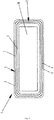
- a film packaging structure for an OLED includes a flexible film 1 for packaging an OLED unit 30.
- the flexible film 1 includes inorganic films 2 and organic films 3 which are alternately stacked with the inorganic films 2.
- the inorganic film 2 between two organic films 3 is provided with a plurality of cavities 4 for separating the inorganic film 2.
- the cavities 4 separate the inorganic film 2 into a plurality of non-connected strip-type inorganic film segments 21 which extends along an extension direction of the organic films 3.
- the shape of the inorganic film segments 21 is not limited to the strip type as shown in the figures, and may be in a regular or irregular shape so long as they are not connected with each other.
- Specific material of the inorganic film 2 may be any suitable inorganic material with a water resistance performance, preferably, for example, alumina, silicon dioxide, magnesium oxide, titanium dioxide, silicon nitride, silicon oxynitride and/or molybdenum oxide, and so on.
- Specific material of the organic film 3 may be any suitable organic filming material with a water resistance performance, preferably, flexible organic filmable material, and further preferably, for example, polyacrylic ester, polyimide, and/or polyethylene, and so on.
- the organic films 3 and the inorganic films 2 may respectively use the same or different material(s).
- the specific number of layers of the organic films 3 and inorganic films 2 can be selected according to requirements.
- a total area of the inorganic film segments 21 is more than a total area of the cavities 4, which is favorable for increasing water resistance performance.
- a moisture absorbent layer 5 is provided in a plurality of cavities 4.
- the moisture absorbent layer 5 may be provided in all of the cavities, or a part of the cavities according to requirements.
- the material of the moisture absorbent layer 5 may be any suitable material with moisture absorption ability, optionally, for example, calcium oxide, silica gel and/or porous silicon, and so on.
- the moisture absorbent layer 5 in the cavities 4 is in contact with the organic film 3 on both sides of the inorganic film 2 respectively so that the inorganic film 2 is separated into a plurality of non-connected inorganic film segments 21 which extends along the extension direction of the organic film 3.
- a plurality of cavities or moisture absorbent layer 5 in an inorganic film 2 and in an adjacent inorganic film 2 are arranged in a stagger manner, and none of them are arranged right oppositely.
- Such a structure helps to increase the water resistance performance, capable of preventing formation of permeable pathway among cavities 4 or moisture absorbent layers 5 between the upper layer and the lower layer.
- the inorganic film 2 has the same thickness as the moisture absorbent layer 5 so as to help to increase the bondability of the inorganic film segments 21 and the moisture absorbent layer 5 with the organic film 3 adjacent thereto, and further increase the water resistance performance of the flexible film 1.
- the inorganic film 2 has a smaller thickness than the organic film 3 so that the organic film 3 can package the inorganic film 2, and further the strength and the durability of the OLED film packaging structure are ensured.
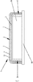
- a film packaging structure for an OLED includes a flexible film 1 in Example 1.
- an OLED unit 30 is entirely packaged by the flexible film 1.
- the OLED unit 30 is not entirely packaged by the flexible film 1, and further includes a substrate 10 for supporting the OLED unit 30.
- the flexible film 1 and the substrate 10 are enclosed to form an accommodating space 20 for accommodating the OLED unit 30.
- the substrate 10 may be a substrate commonly used in the art.
- An OLED device includes an OLED unit and a film packaging structure for an OLED according to the embodiment of the disclosure for packaging the OLED unit.
- a display apparatus includes an OLED device according to the present disclosure.
- the film packaging structure for the OLED of the disclosure makes the inorganic film to be a discontinuous structure in a multilayered packaging structure, and coats moisture absorbent layer in cavities of the same inorganic film.
- the hollow arrow in Fig. 3 shows a penetrating route of water molecules.
- the film packaging structure for the OLED in the disclosure guides water molecules to penetrate on the one hand, and absorbs the water molecules on their penetration path on the other hand, such that the water resistance performance of multilayered film packaging structure is increased. Because the inorganic film is separated into a plurality of non-connected inorganic film segments with smaller area, the chance for rupture during bending reduces, and the water resistance performance is maintained substantially.
- the inorganic film in the film packaging structure for the OLED of Examples 1 and 2 may be made by physical or chemical deposition, then the discontinuous regular arrangement may be formed via the method of metal mask plate or dry etching and separating.
- the moisture absorbent layer may be formed by coating or physical deposition, followed by finally arranging it only in gaps of the inorganic film via method of ashing, separating and dry etching, and so on. And then, precursors of organic film may be formed by spraying and scrapping.
- the organic film may be formed by UV curing or heat curing. And then the steps of forming the inorganic film, the moisture absorbent layer and the organic layer may be repeated to finally obtain the film packaging structure for the OLED in the embodiments of the disclosure.
- the film packaging structures for the OLED, the OLED device, and the display apparatus in all embodiments according to the present disclosure use inorganic films and organic film which are alternately stacked with the inorganic film, and the inorganic film is formed as non-connected structure to achieve better water resistance performance, and meanwhile, the structure is easy to facilitate preparation.
Landscapes
- Chemical & Material Sciences (AREA)
- Inorganic Chemistry (AREA)
- Physics & Mathematics (AREA)
- Optics & Photonics (AREA)
- Electroluminescent Light Sources (AREA)
- Laminated Bodies (AREA)
Claims (13)
- Folienhäusungsstruktur für eine OLED, umfassend: eine flexible Folie (1) zum Häusen einer OLED-Einheit (30), wobei die flexible Folie (1) mindestens eine Schicht aus anorganischer Folie (2) und mindestens eine Schicht aus organischer Folie (3) umfasst, die abwechselnd mit der mindestens einen Schicht aus anorganischer Folie (2) gestapelt ist, wobei jede Schicht aus organischer Folie (3) in der mindestens einen Schicht aus organischer Folie (3) eine einstückige Folie ist und jede Schicht aus anorganischer Folie (2) in der mindestens einen Schicht aus anorganischer Folie (2) mehrere nicht verbundene Segmente (21) aus anorganischer Folie umfasst,
wobei
mehrere Vertiefungen (4) zwischen den mehreren nicht verbundenen Segmenten (21) aus anorganischer Folie bereitgestellt sind, um die mehreren nicht verbundenen Segmente (21) aus anorganischer Folie nicht miteinander verbunden herzustellen, dadurch gekennzeichnet, dass eine feuchtigkeitsabsorbierende Schicht (5) in einem Teil oder allen der mehreren Vertiefungen (4) bereitgestellt ist. - Folienhäusungsstruktur für eine OLED nach Anspruch 1, wobei die Vertiefungen (4) in der anorganischen Folie (2) zwischen zwei Schichten aus organischer Folie (3) bereitgestellt sind, um die anorganische Folie (2) in mehrere nicht verbundene, streifenartige Segmente (21) aus anorganischer Folie zu trennen, die sich entlang der organischen Folie (3) erstrecken.
- Folienhäusungsstruktur für eine OLED nach Anspruch 1 oder Anspruch 2, wobei die feuchtigkeitsabsorbierende Schicht (5) in den Vertiefungen (4) in Kontakt mit einer angrenzenden organischen Folie (3) steht, sodass die anorganische Folie (2) in mehrere nicht verbundene Segmente (21) aus anorganischer Folie getrennt ist.
- Folienhäusungsstruktur für eine OLED nach einem der Ansprüche 1 bis 3, wobei die mehreren Vertiefungen (4) in der anorganischen Folie (2) und die mehreren Vertiefungen (4) in einer angrenzenden anorganischen Folie (2) in versetzter Weise angeordnet sind.
- Folienhäusungsstruktur für eine OLED nach Anspruch 1 oder Anspruch 3, wobei die anorganische Folie (2) die gleiche Dicke aufweist wie die feuchtigkeitsabsorbierende Schicht (5).
- Folienhäusungsstruktur für eine OLED nach einem der Ansprüche 1 bis 5, wobei die anorganische Folie (2) eine geringere Dicke aufweist als die organische Folie (3).
- Folienhäusungsstruktur für eine OLED nach einem der Ansprüche 1 bis 6, ferner ein Substrat (10) zum Tragen der OLED-Einheit (30) umfassend, wobei die flexible Folie (1) und das Substrat (10) umschlossen sind, um einen Aufnahmeraum zum Aufnehmen der OLED-Einheit (30) zu bilden.
- Folienhäusungsstruktur für eine OLED nach einem der Ansprüche 1 bis 7, wobei die anorganische Folie (2) ein anorganisches Material mit einem Wasserfestigkeitsverhalten umfasst und die organische Folie (3) ein organisches, zu einer Folie verarbeitbares Material mit einem Wasserfestigkeitsverhalten umfasst.
- Folienhäusungsstruktur für eine OLED nach einem der Ansprüche 1 bis 8, wobei die anorganische Folie (2) Aluminiumoxid, Siliciumdioxid, Magensiumoxid, Titandioxid, Siliciumnitrid, Siliciumoxynitrid und/oder Molybdänoxid umfasst,
die organische Folie (3) Polyacrylester, Polyimid und/oder Polyethylen umfasst. - Folienhäusungsstruktur für eine OLED nach einem der Ansprüche 1 bis 9, wobei die feuchtigkeitsabsorbierende Schicht (5) Calciumoxid, Silicagel und/oder poröses Silicium umfasst.
- Folienhäusungsstruktur für eine OLED nach einem der Ansprüche 1 bis 10, wobei eine Gesamtfläche der Segmente (21) aus anorganischer Folie in der mindestens einen Schicht aus anorganischer Folie (2) größer als eine Gesamtfläche der Vertiefungen (4) ist.
- OLED-Bauelement, eine OLED-Einheit (30) und die Folienhäusungsstruktur für eine OLED nach einem der Ansprüche 1 bis 10 zum Häusen der OLED-Einheit (30) umfassend.
- Anzeigevorrichtung, das OLED-Bauelement nach Anspruch 12 umfassend.
Applications Claiming Priority (2)
| Application Number | Priority Date | Filing Date | Title |
|---|---|---|---|
| CN201310711653.6A CN103715366A (zh) | 2013-12-20 | 2013-12-20 | Oled薄膜封装结构、oled器件以及显示装置 |
| PCT/CN2014/078273 WO2015089998A1 (zh) | 2013-12-20 | 2014-05-23 | Oled用薄膜封装结构、oled器件以及显示装置 |
Publications (3)
| Publication Number | Publication Date |
|---|---|
| EP3086381A1 EP3086381A1 (de) | 2016-10-26 |
| EP3086381A4 EP3086381A4 (de) | 2017-08-23 |
| EP3086381B1 true EP3086381B1 (de) | 2020-10-28 |
Family
ID=50408155
Family Applications (1)
| Application Number | Title | Priority Date | Filing Date |
|---|---|---|---|
| EP14859325.4A Not-in-force EP3086381B1 (de) | 2013-12-20 | 2014-05-23 | Dünnschicht-verkapselungsaufbau für oled, oled-vorrichtung und anzeigevorrichtung |
Country Status (4)
| Country | Link |
|---|---|
| US (1) | US9472784B2 (de) |
| EP (1) | EP3086381B1 (de) |
| CN (1) | CN103715366A (de) |
| WO (1) | WO2015089998A1 (de) |
Families Citing this family (31)
| Publication number | Priority date | Publication date | Assignee | Title |
|---|---|---|---|---|
| CN103715366A (zh) * | 2013-12-20 | 2014-04-09 | 京东方科技集团股份有限公司 | Oled薄膜封装结构、oled器件以及显示装置 |
| CN104269426A (zh) * | 2014-09-01 | 2015-01-07 | 京东方科技集团股份有限公司 | 一种显示面板及其制备方法和显示装置 |
| JP2016072127A (ja) * | 2014-09-30 | 2016-05-09 | ソニー株式会社 | 有機el表示装置およびその製造方法、並びに電子機器 |
| CN104538425B (zh) * | 2014-12-19 | 2018-01-12 | 上海天马微电子有限公司 | 一种阻挡膜及其制作方法、显示装置 |
| KR102417119B1 (ko) * | 2015-02-11 | 2022-07-06 | 삼성디스플레이 주식회사 | 플렉서블 디스플레이 장치 |
| US9614183B2 (en) | 2015-04-01 | 2017-04-04 | Apple Inc. | Organic light-emitting diode displays with crack detection and crack propagation prevention circuitry |
| CN104733507B (zh) * | 2015-04-09 | 2018-05-01 | 京东方科技集团股份有限公司 | 柔性显示装置和柔性显示装置的封装方法 |
| CN104900812A (zh) | 2015-04-23 | 2015-09-09 | 京东方科技集团股份有限公司 | 薄膜封装结构及其制作方法和显示装置 |
| CN105206763B (zh) * | 2015-10-21 | 2018-01-23 | 京东方科技集团股份有限公司 | 柔性显示器及其制造方法 |
| CN105355645B (zh) * | 2015-11-06 | 2019-07-26 | 上海天马微电子有限公司 | 一种柔性显示面板及其制造方法、显示装置 |
| WO2017113314A1 (zh) * | 2015-12-31 | 2017-07-06 | 深圳市柔宇科技有限公司 | 封装结构、柔性显示屏及封装结构制作方法 |
| JP2017152256A (ja) * | 2016-02-25 | 2017-08-31 | 株式会社ジャパンディスプレイ | 表示装置 |
| CN105702624A (zh) * | 2016-03-30 | 2016-06-22 | 武汉华星光电技术有限公司 | 叠层柔性基板及制作方法 |
| CN106997930B (zh) * | 2017-03-03 | 2019-04-12 | 上海天马有机发光显示技术有限公司 | 柔性显示面板及显示装置 |
| CN106848106B (zh) * | 2017-04-19 | 2019-03-29 | 京东方科技集团股份有限公司 | 有机电致发光装置封装结构及其制作方法、显示装置 |
| CN107195794B (zh) | 2017-06-06 | 2019-07-30 | 京东方科技集团股份有限公司 | 一种柔性显示基板及其制作方法、显示面板、显示装置 |
| CN109585669B (zh) * | 2017-09-29 | 2024-05-17 | 京东方科技集团股份有限公司 | 薄膜封装结构及其制备方法 |
| CN107863454A (zh) * | 2017-11-21 | 2018-03-30 | 武汉华星光电半导体显示技术有限公司 | 柔性oled显示面板及其封装方法 |
| US20190229299A1 (en) * | 2018-01-24 | 2019-07-25 | Wuhan China Star Optoelecronics Semiconductor Display Technology Co., LTd. | Thin-film packaging method for an oled device and oled device |
| CN108305954B (zh) * | 2018-01-24 | 2020-07-31 | 武汉华星光电半导体显示技术有限公司 | Oled器件的薄膜封装方法及oled器件 |
| CN110085740B (zh) * | 2018-01-25 | 2022-01-11 | 绵阳京东方光电科技有限公司 | 柔性基板及其制作方法、面板以及电子装置 |
| WO2019180846A1 (ja) * | 2018-03-20 | 2019-09-26 | シャープ株式会社 | 成膜用マスクおよびそれを用いた表示装置の製造方法 |
| CN108565360A (zh) * | 2018-04-10 | 2018-09-21 | 深圳市华星光电技术有限公司 | 一种oled显示装置及其制备方法 |
| CN108428731B (zh) * | 2018-05-17 | 2021-01-01 | 武汉华星光电半导体显示技术有限公司 | 柔性oled显示面板及柔性oled显示装置 |
| CN109346622A (zh) * | 2018-10-19 | 2019-02-15 | 武汉华星光电半导体显示技术有限公司 | Oled阵列基板及其制作方法 |
| CN109671750B (zh) * | 2018-12-13 | 2021-04-20 | 云谷(固安)科技有限公司 | 一种显示面板、显示面板的制备方法及制备设备 |
| JP6814230B2 (ja) * | 2019-01-11 | 2021-01-13 | 株式会社Joled | 発光パネル、発光装置および電子機器 |
| CN111192972A (zh) * | 2019-03-18 | 2020-05-22 | 广东聚华印刷显示技术有限公司 | 薄膜封装结构及其制备方法和显示装置 |
| CN109872631B (zh) * | 2019-03-18 | 2021-04-27 | 京东方科技集团股份有限公司 | 一种可拉伸显示模组及其制作方法和显示设备 |
| CN111341940A (zh) * | 2020-03-18 | 2020-06-26 | 上海晶合光电科技有限公司 | 一种oled器件封装结构及其制备方法 |
| CN113013352B (zh) * | 2021-01-29 | 2023-07-21 | 固安翌光科技有限公司 | 一种薄膜封装结构及有机光电器件 |
Family Cites Families (23)
| Publication number | Priority date | Publication date | Assignee | Title |
|---|---|---|---|---|
| WO2006014591A2 (en) * | 2004-07-08 | 2006-02-09 | Itn Energy Systems, Inc. | Permeation barriers for flexible electronics |
| KR100647340B1 (ko) * | 2006-01-11 | 2006-11-23 | 삼성전자주식회사 | 평판표시장치 |
| KR20080006304A (ko) * | 2006-07-12 | 2008-01-16 | 삼성전자주식회사 | 유기 발광 표시 장치 및 그 제조 방법 |
| US7663312B2 (en) * | 2006-07-24 | 2010-02-16 | Munisamy Anandan | Flexible OLED light source |
| JP2009076232A (ja) * | 2007-09-19 | 2009-04-09 | Fujifilm Corp | 環境感受性デバイス、環境感受性素子の封止方法 |
| CN101128074A (zh) * | 2007-09-20 | 2008-02-20 | 清华大学 | 一种有机电致发光器件及其制备方法 |
| JP2009092908A (ja) * | 2007-10-09 | 2009-04-30 | Canon Inc | 表示装置及びその製造方法 |
| JP4920548B2 (ja) * | 2007-10-31 | 2012-04-18 | 株式会社 日立ディスプレイズ | 表示装置 |
| KR101492630B1 (ko) * | 2008-06-10 | 2015-03-03 | 엘지디스플레이 주식회사 | 유기발광다이오드 표시소자 |
| KR101084267B1 (ko) * | 2009-02-26 | 2011-11-16 | 삼성모바일디스플레이주식회사 | 유기 발광 표시 장치 및 그 제조 방법 |
| KR101097318B1 (ko) * | 2009-11-25 | 2011-12-21 | 삼성모바일디스플레이주식회사 | 유기 발광 소자 및 이의 제조 방법 |
| KR101155904B1 (ko) | 2010-01-04 | 2012-06-20 | 삼성모바일디스플레이주식회사 | 유기 발광 표시 장치 |
| KR20110114325A (ko) * | 2010-04-13 | 2011-10-19 | 삼성모바일디스플레이주식회사 | 표시 장치 |
| EP2445028A1 (de) * | 2010-10-25 | 2012-04-25 | Nederlandse Organisatie voor toegepast -natuurwetenschappelijk onderzoek TNO | Optoelektrische Vorrichtung und Verfahren zur Herstellung einer optoelektrischen Vorrichtung |
| KR101937999B1 (ko) * | 2010-12-28 | 2019-01-15 | 엘지디스플레이 주식회사 | 유기전계발광표시장치 |
| KR101863853B1 (ko) * | 2011-07-29 | 2018-06-04 | 삼성디스플레이 주식회사 | 유기 발광 표시장치 및 그 제조방법 |
| CN102437288A (zh) * | 2011-11-16 | 2012-05-02 | 四川长虹电器股份有限公司 | 有机电致发光器件的封装结构 |
| CN103165821A (zh) * | 2011-12-08 | 2013-06-19 | 上海天马微电子有限公司 | Oled显示模组封装结构 |
| CN103258955B (zh) * | 2012-02-20 | 2016-02-03 | 中国科学院微电子研究所 | 有机电子器件的封装方法 |
| CN103325953B (zh) * | 2012-03-19 | 2016-02-10 | 瀚宇彩晶股份有限公司 | 有机发光二极管封装及其封装方法 |
| TWI520215B (zh) * | 2012-09-19 | 2016-02-01 | 友達光電股份有限公司 | 元件基板及其製造方法 |
| CN203134801U (zh) * | 2012-11-21 | 2013-08-14 | 京东方科技集团股份有限公司 | 一种oled显示装置 |
| CN103715366A (zh) | 2013-12-20 | 2014-04-09 | 京东方科技集团股份有限公司 | Oled薄膜封装结构、oled器件以及显示装置 |
-
2013
- 2013-12-20 CN CN201310711653.6A patent/CN103715366A/zh active Pending
-
2014
- 2014-05-23 WO PCT/CN2014/078273 patent/WO2015089998A1/zh not_active Ceased
- 2014-05-23 EP EP14859325.4A patent/EP3086381B1/de not_active Not-in-force
- 2014-05-23 US US14/415,481 patent/US9472784B2/en active Active
Non-Patent Citations (1)
| Title |
|---|
| None * |
Also Published As
| Publication number | Publication date |
|---|---|
| WO2015089998A1 (zh) | 2015-06-25 |
| US20160043347A1 (en) | 2016-02-11 |
| US9472784B2 (en) | 2016-10-18 |
| CN103715366A (zh) | 2014-04-09 |
| EP3086381A4 (de) | 2017-08-23 |
| EP3086381A1 (de) | 2016-10-26 |
Similar Documents
| Publication | Publication Date | Title |
|---|---|---|
| EP3086381B1 (de) | Dünnschicht-verkapselungsaufbau für oled, oled-vorrichtung und anzeigevorrichtung | |
| US12575258B2 (en) | Display apparatus and method of manufacturing the same | |
| KR102402905B1 (ko) | 유기 발광 표시장치 | |
| EP2830095B1 (de) | Organische lichtemittierende Anzeigevorrichtung und Herstellungsverfahren dafür | |
| TWI492436B (zh) | 可撓式顯示面板 | |
| US20120161197A1 (en) | Flexible organic light-emitting display device and method of manufacturing the same | |
| US20130126915A1 (en) | Flexible active device array substrate and organic electroluminescent device having the same | |
| KR101410102B1 (ko) | 유기발광 표시장치 | |
| US20190058158A1 (en) | Package of electronic device and display panel | |
| EP3002800B1 (de) | Organische lichtemittierende anzeigevorrichtung | |
| KR102351003B1 (ko) | 유기발광표시장치 및 그 제조 방법 | |
| TW201419082A (zh) | 製造顯示設備之方法 | |
| KR20120075705A (ko) | 보호막 및 이를 포함하는 전자 소자 | |
| TWI635635B (zh) | 元件構造體及元件構造體之製造方法 | |
| KR102318266B1 (ko) | 유기 발광 표시 장치 및 그 제조 방법 | |
| KR101120642B1 (ko) | 투명한 밀봉 플라스틱 필름 및 그 제조방법과 이를 구비한 디스플레이 기판 |
Legal Events
| Date | Code | Title | Description |
|---|---|---|---|
| PUAI | Public reference made under article 153(3) epc to a published international application that has entered the european phase |
Free format text: ORIGINAL CODE: 0009012 |
|
| 17P | Request for examination filed |
Effective date: 20150513 |
|
| AK | Designated contracting states |
Kind code of ref document: A1 Designated state(s): AL AT BE BG CH CY CZ DE DK EE ES FI FR GB GR HR HU IE IS IT LI LT LU LV MC MK MT NL NO PL PT RO RS SE SI SK SM TR |
|
| AX | Request for extension of the european patent |
Extension state: BA ME |
|
| DAX | Request for extension of the european patent (deleted) | ||
| A4 | Supplementary search report drawn up and despatched |
Effective date: 20170725 |
|
| RIC1 | Information provided on ipc code assigned before grant |
Ipc: H01L 51/52 20060101AFI20170719BHEP |
|
| GRAP | Despatch of communication of intention to grant a patent |
Free format text: ORIGINAL CODE: EPIDOSNIGR1 |
|
| STAA | Information on the status of an ep patent application or granted ep patent |
Free format text: STATUS: GRANT OF PATENT IS INTENDED |
|
| INTG | Intention to grant announced |
Effective date: 20200616 |
|
| GRAS | Grant fee paid |
Free format text: ORIGINAL CODE: EPIDOSNIGR3 |
|
| GRAA | (expected) grant |
Free format text: ORIGINAL CODE: 0009210 |
|
| STAA | Information on the status of an ep patent application or granted ep patent |
Free format text: STATUS: THE PATENT HAS BEEN GRANTED |
|
| AK | Designated contracting states |
Kind code of ref document: B1 Designated state(s): AL AT BE BG CH CY CZ DE DK EE ES FI FR GB GR HR HU IE IS IT LI LT LU LV MC MK MT NL NO PL PT RO RS SE SI SK SM TR |
|
| REG | Reference to a national code |
Ref country code: GB Ref legal event code: FG4D |
|
| REG | Reference to a national code |
Ref country code: CH Ref legal event code: EP |
|
| REG | Reference to a national code |
Ref country code: DE Ref legal event code: R096 Ref document number: 602014071813 Country of ref document: DE |
|
| REG | Reference to a national code |
Ref country code: AT Ref legal event code: REF Ref document number: 1329120 Country of ref document: AT Kind code of ref document: T Effective date: 20201115 |
|
| REG | Reference to a national code |
Ref country code: IE Ref legal event code: FG4D |
|
| REG | Reference to a national code |
Ref country code: AT Ref legal event code: MK05 Ref document number: 1329120 Country of ref document: AT Kind code of ref document: T Effective date: 20201028 |
|
| REG | Reference to a national code |
Ref country code: NL Ref legal event code: MP Effective date: 20201028 |
|
| PG25 | Lapsed in a contracting state [announced via postgrant information from national office to epo] |
Ref country code: GR Free format text: LAPSE BECAUSE OF FAILURE TO SUBMIT A TRANSLATION OF THE DESCRIPTION OR TO PAY THE FEE WITHIN THE PRESCRIBED TIME-LIMIT Effective date: 20210129 Ref country code: PT Free format text: LAPSE BECAUSE OF FAILURE TO SUBMIT A TRANSLATION OF THE DESCRIPTION OR TO PAY THE FEE WITHIN THE PRESCRIBED TIME-LIMIT Effective date: 20210301 Ref country code: NL Free format text: LAPSE BECAUSE OF FAILURE TO SUBMIT A TRANSLATION OF THE DESCRIPTION OR TO PAY THE FEE WITHIN THE PRESCRIBED TIME-LIMIT Effective date: 20201028 Ref country code: NO Free format text: LAPSE BECAUSE OF FAILURE TO SUBMIT A TRANSLATION OF THE DESCRIPTION OR TO PAY THE FEE WITHIN THE PRESCRIBED TIME-LIMIT Effective date: 20210128 Ref country code: RS Free format text: LAPSE BECAUSE OF FAILURE TO SUBMIT A TRANSLATION OF THE DESCRIPTION OR TO PAY THE FEE WITHIN THE PRESCRIBED TIME-LIMIT Effective date: 20201028 Ref country code: FI Free format text: LAPSE BECAUSE OF FAILURE TO SUBMIT A TRANSLATION OF THE DESCRIPTION OR TO PAY THE FEE WITHIN THE PRESCRIBED TIME-LIMIT Effective date: 20201028 |
|
| REG | Reference to a national code |
Ref country code: LT Ref legal event code: MG4D |
|
| PG25 | Lapsed in a contracting state [announced via postgrant information from national office to epo] |
Ref country code: ES Free format text: LAPSE BECAUSE OF FAILURE TO SUBMIT A TRANSLATION OF THE DESCRIPTION OR TO PAY THE FEE WITHIN THE PRESCRIBED TIME-LIMIT Effective date: 20201028 Ref country code: AT Free format text: LAPSE BECAUSE OF FAILURE TO SUBMIT A TRANSLATION OF THE DESCRIPTION OR TO PAY THE FEE WITHIN THE PRESCRIBED TIME-LIMIT Effective date: 20201028 Ref country code: BG Free format text: LAPSE BECAUSE OF FAILURE TO SUBMIT A TRANSLATION OF THE DESCRIPTION OR TO PAY THE FEE WITHIN THE PRESCRIBED TIME-LIMIT Effective date: 20210128 Ref country code: IS Free format text: LAPSE BECAUSE OF FAILURE TO SUBMIT A TRANSLATION OF THE DESCRIPTION OR TO PAY THE FEE WITHIN THE PRESCRIBED TIME-LIMIT Effective date: 20210228 Ref country code: SE Free format text: LAPSE BECAUSE OF FAILURE TO SUBMIT A TRANSLATION OF THE DESCRIPTION OR TO PAY THE FEE WITHIN THE PRESCRIBED TIME-LIMIT Effective date: 20201028 Ref country code: PL Free format text: LAPSE BECAUSE OF FAILURE TO SUBMIT A TRANSLATION OF THE DESCRIPTION OR TO PAY THE FEE WITHIN THE PRESCRIBED TIME-LIMIT Effective date: 20201028 Ref country code: LV Free format text: LAPSE BECAUSE OF FAILURE TO SUBMIT A TRANSLATION OF THE DESCRIPTION OR TO PAY THE FEE WITHIN THE PRESCRIBED TIME-LIMIT Effective date: 20201028 |
|
| PG25 | Lapsed in a contracting state [announced via postgrant information from national office to epo] |
Ref country code: HR Free format text: LAPSE BECAUSE OF FAILURE TO SUBMIT A TRANSLATION OF THE DESCRIPTION OR TO PAY THE FEE WITHIN THE PRESCRIBED TIME-LIMIT Effective date: 20201028 |
|
| REG | Reference to a national code |
Ref country code: DE Ref legal event code: R097 Ref document number: 602014071813 Country of ref document: DE |
|
| PG25 | Lapsed in a contracting state [announced via postgrant information from national office to epo] |
Ref country code: CZ Free format text: LAPSE BECAUSE OF FAILURE TO SUBMIT A TRANSLATION OF THE DESCRIPTION OR TO PAY THE FEE WITHIN THE PRESCRIBED TIME-LIMIT Effective date: 20201028 Ref country code: EE Free format text: LAPSE BECAUSE OF FAILURE TO SUBMIT A TRANSLATION OF THE DESCRIPTION OR TO PAY THE FEE WITHIN THE PRESCRIBED TIME-LIMIT Effective date: 20201028 Ref country code: SM Free format text: LAPSE BECAUSE OF FAILURE TO SUBMIT A TRANSLATION OF THE DESCRIPTION OR TO PAY THE FEE WITHIN THE PRESCRIBED TIME-LIMIT Effective date: 20201028 Ref country code: RO Free format text: LAPSE BECAUSE OF FAILURE TO SUBMIT A TRANSLATION OF THE DESCRIPTION OR TO PAY THE FEE WITHIN THE PRESCRIBED TIME-LIMIT Effective date: 20201028 Ref country code: SK Free format text: LAPSE BECAUSE OF FAILURE TO SUBMIT A TRANSLATION OF THE DESCRIPTION OR TO PAY THE FEE WITHIN THE PRESCRIBED TIME-LIMIT Effective date: 20201028 Ref country code: LT Free format text: LAPSE BECAUSE OF FAILURE TO SUBMIT A TRANSLATION OF THE DESCRIPTION OR TO PAY THE FEE WITHIN THE PRESCRIBED TIME-LIMIT Effective date: 20201028 |
|
| PG25 | Lapsed in a contracting state [announced via postgrant information from national office to epo] |
Ref country code: DK Free format text: LAPSE BECAUSE OF FAILURE TO SUBMIT A TRANSLATION OF THE DESCRIPTION OR TO PAY THE FEE WITHIN THE PRESCRIBED TIME-LIMIT Effective date: 20201028 |
|
| PLBE | No opposition filed within time limit |
Free format text: ORIGINAL CODE: 0009261 |
|
| STAA | Information on the status of an ep patent application or granted ep patent |
Free format text: STATUS: NO OPPOSITION FILED WITHIN TIME LIMIT |
|
| 26N | No opposition filed |
Effective date: 20210729 |
|
| PG25 | Lapsed in a contracting state [announced via postgrant information from national office to epo] |
Ref country code: AL Free format text: LAPSE BECAUSE OF FAILURE TO SUBMIT A TRANSLATION OF THE DESCRIPTION OR TO PAY THE FEE WITHIN THE PRESCRIBED TIME-LIMIT Effective date: 20201028 Ref country code: IT Free format text: LAPSE BECAUSE OF FAILURE TO SUBMIT A TRANSLATION OF THE DESCRIPTION OR TO PAY THE FEE WITHIN THE PRESCRIBED TIME-LIMIT Effective date: 20201028 |
|
| PG25 | Lapsed in a contracting state [announced via postgrant information from national office to epo] |
Ref country code: SI Free format text: LAPSE BECAUSE OF FAILURE TO SUBMIT A TRANSLATION OF THE DESCRIPTION OR TO PAY THE FEE WITHIN THE PRESCRIBED TIME-LIMIT Effective date: 20201028 |
|
| REG | Reference to a national code |
Ref country code: CH Ref legal event code: PL |
|
| GBPC | Gb: european patent ceased through non-payment of renewal fee |
Effective date: 20210523 |
|
| PG25 | Lapsed in a contracting state [announced via postgrant information from national office to epo] |
Ref country code: CH Free format text: LAPSE BECAUSE OF NON-PAYMENT OF DUE FEES Effective date: 20210531 Ref country code: LI Free format text: LAPSE BECAUSE OF NON-PAYMENT OF DUE FEES Effective date: 20210531 Ref country code: LU Free format text: LAPSE BECAUSE OF NON-PAYMENT OF DUE FEES Effective date: 20210523 Ref country code: MC Free format text: LAPSE BECAUSE OF FAILURE TO SUBMIT A TRANSLATION OF THE DESCRIPTION OR TO PAY THE FEE WITHIN THE PRESCRIBED TIME-LIMIT Effective date: 20201028 |
|
| REG | Reference to a national code |
Ref country code: BE Ref legal event code: MM Effective date: 20210531 |
|
| PG25 | Lapsed in a contracting state [announced via postgrant information from national office to epo] |
Ref country code: IE Free format text: LAPSE BECAUSE OF NON-PAYMENT OF DUE FEES Effective date: 20210523 Ref country code: GB Free format text: LAPSE BECAUSE OF NON-PAYMENT OF DUE FEES Effective date: 20210523 |
|
| PG25 | Lapsed in a contracting state [announced via postgrant information from national office to epo] |
Ref country code: IS Free format text: LAPSE BECAUSE OF FAILURE TO SUBMIT A TRANSLATION OF THE DESCRIPTION OR TO PAY THE FEE WITHIN THE PRESCRIBED TIME-LIMIT Effective date: 20210228 Ref country code: FR Free format text: LAPSE BECAUSE OF NON-PAYMENT OF DUE FEES Effective date: 20210531 |
|
| PG25 | Lapsed in a contracting state [announced via postgrant information from national office to epo] |
Ref country code: BE Free format text: LAPSE BECAUSE OF NON-PAYMENT OF DUE FEES Effective date: 20210531 |
|
| REG | Reference to a national code |
Ref country code: DE Ref legal event code: R079 Ref document number: 602014071813 Country of ref document: DE Free format text: PREVIOUS MAIN CLASS: H01L0051520000 Ipc: H10K0050800000 |
|
| PG25 | Lapsed in a contracting state [announced via postgrant information from national office to epo] |
Ref country code: HU Free format text: LAPSE BECAUSE OF FAILURE TO SUBMIT A TRANSLATION OF THE DESCRIPTION OR TO PAY THE FEE WITHIN THE PRESCRIBED TIME-LIMIT; INVALID AB INITIO Effective date: 20140523 |
|
| PG25 | Lapsed in a contracting state [announced via postgrant information from national office to epo] |
Ref country code: CY Free format text: LAPSE BECAUSE OF FAILURE TO SUBMIT A TRANSLATION OF THE DESCRIPTION OR TO PAY THE FEE WITHIN THE PRESCRIBED TIME-LIMIT Effective date: 20201028 |
|
| PG25 | Lapsed in a contracting state [announced via postgrant information from national office to epo] |
Ref country code: MK Free format text: LAPSE BECAUSE OF FAILURE TO SUBMIT A TRANSLATION OF THE DESCRIPTION OR TO PAY THE FEE WITHIN THE PRESCRIBED TIME-LIMIT Effective date: 20201028 |
|
| PGFP | Annual fee paid to national office [announced via postgrant information from national office to epo] |
Ref country code: DE Payment date: 20240517 Year of fee payment: 11 |
|
| PG25 | Lapsed in a contracting state [announced via postgrant information from national office to epo] |
Ref country code: MT Free format text: LAPSE BECAUSE OF FAILURE TO SUBMIT A TRANSLATION OF THE DESCRIPTION OR TO PAY THE FEE WITHIN THE PRESCRIBED TIME-LIMIT Effective date: 20201028 |
|
| REG | Reference to a national code |
Ref country code: DE Ref legal event code: R119 Ref document number: 602014071813 Country of ref document: DE |
|
| PG25 | Lapsed in a contracting state [announced via postgrant information from national office to epo] |
Ref country code: TR Free format text: LAPSE BECAUSE OF FAILURE TO SUBMIT A TRANSLATION OF THE DESCRIPTION OR TO PAY THE FEE WITHIN THE PRESCRIBED TIME-LIMIT Effective date: 20201028 |
|
| PG25 | Lapsed in a contracting state [announced via postgrant information from national office to epo] |
Ref country code: DE Free format text: LAPSE BECAUSE OF NON-PAYMENT OF DUE FEES Effective date: 20251202 |