EP3086150B1 - Data bus-in-a-box (bib) system design and implementation - Google Patents
Data bus-in-a-box (bib) system design and implementation Download PDFInfo
- Publication number
- EP3086150B1 EP3086150B1 EP15193003.9A EP15193003A EP3086150B1 EP 3086150 B1 EP3086150 B1 EP 3086150B1 EP 15193003 A EP15193003 A EP 15193003A EP 3086150 B1 EP3086150 B1 EP 3086150B1
- Authority
- EP
- European Patent Office
- Prior art keywords
- box
- omc
- transmit
- receive
- tile
- Prior art date
- Legal status (The legal status is an assumption and is not a legal conclusion. Google has not performed a legal analysis and makes no representation as to the accuracy of the status listed.)
- Active
Links
Images


Classifications
-
- G—PHYSICS
- G02—OPTICS
- G02B—OPTICAL ELEMENTS, SYSTEMS OR APPARATUS
- G02B6/00—Light guides; Structural details of arrangements comprising light guides and other optical elements, e.g. couplings
- G02B6/24—Coupling light guides
- G02B6/42—Coupling light guides with opto-electronic elements
- G02B6/4201—Packages, e.g. shape, construction, internal or external details
- G02B6/4287—Optical modules with tapping or launching means through the surface of the waveguide
-
- G—PHYSICS
- G02—OPTICS
- G02B—OPTICAL ELEMENTS, SYSTEMS OR APPARATUS
- G02B6/00—Light guides; Structural details of arrangements comprising light guides and other optical elements, e.g. couplings
- G02B6/44—Mechanical structures for providing tensile strength and external protection for fibres, e.g. optical transmission cables
- G02B6/4439—Auxiliary devices
- G02B6/444—Systems or boxes with surplus lengths
- G02B6/4441—Boxes
- G02B6/4446—Cable boxes, e.g. splicing boxes with two or more multi fibre cables
- G02B6/44465—Seals
-
- G—PHYSICS
- G02—OPTICS
- G02B—OPTICAL ELEMENTS, SYSTEMS OR APPARATUS
- G02B6/00—Light guides; Structural details of arrangements comprising light guides and other optical elements, e.g. couplings
- G02B6/24—Coupling light guides
- G02B6/36—Mechanical coupling means
- G02B6/38—Mechanical coupling means having fibre to fibre mating means
-
- B—PERFORMING OPERATIONS; TRANSPORTING
- B32—LAYERED PRODUCTS
- B32B—LAYERED PRODUCTS, i.e. PRODUCTS BUILT-UP OF STRATA OF FLAT OR NON-FLAT, e.g. CELLULAR OR HONEYCOMB, FORM
- B32B37/00—Methods or apparatus for laminating, e.g. by curing or by ultrasonic bonding
- B32B37/12—Methods or apparatus for laminating, e.g. by curing or by ultrasonic bonding characterised by using adhesives
- B32B37/1284—Application of adhesive
-
- B—PERFORMING OPERATIONS; TRANSPORTING
- B32—LAYERED PRODUCTS
- B32B—LAYERED PRODUCTS, i.e. PRODUCTS BUILT-UP OF STRATA OF FLAT OR NON-FLAT, e.g. CELLULAR OR HONEYCOMB, FORM
- B32B37/00—Methods or apparatus for laminating, e.g. by curing or by ultrasonic bonding
- B32B37/14—Methods or apparatus for laminating, e.g. by curing or by ultrasonic bonding characterised by the properties of the layers
- B32B37/142—Laminating of sheets, panels or inserts, e.g. stiffeners, by wrapping in at least one outer layer, or inserting into a preformed pocket
-
- B—PERFORMING OPERATIONS; TRANSPORTING
- B32—LAYERED PRODUCTS
- B32B—LAYERED PRODUCTS, i.e. PRODUCTS BUILT-UP OF STRATA OF FLAT OR NON-FLAT, e.g. CELLULAR OR HONEYCOMB, FORM
- B32B37/00—Methods or apparatus for laminating, e.g. by curing or by ultrasonic bonding
- B32B37/14—Methods or apparatus for laminating, e.g. by curing or by ultrasonic bonding characterised by the properties of the layers
- B32B37/16—Methods or apparatus for laminating, e.g. by curing or by ultrasonic bonding characterised by the properties of the layers with all layers existing as coherent layers before laminating
- B32B37/18—Methods or apparatus for laminating, e.g. by curing or by ultrasonic bonding characterised by the properties of the layers with all layers existing as coherent layers before laminating involving the assembly of discrete sheets or panels only
-
- B—PERFORMING OPERATIONS; TRANSPORTING
- B32—LAYERED PRODUCTS
- B32B—LAYERED PRODUCTS, i.e. PRODUCTS BUILT-UP OF STRATA OF FLAT OR NON-FLAT, e.g. CELLULAR OR HONEYCOMB, FORM
- B32B38/00—Ancillary operations in connection with laminating processes
- B32B38/0004—Cutting, tearing or severing, e.g. bursting; Cutter details
-
- B—PERFORMING OPERATIONS; TRANSPORTING
- B32—LAYERED PRODUCTS
- B32B—LAYERED PRODUCTS, i.e. PRODUCTS BUILT-UP OF STRATA OF FLAT OR NON-FLAT, e.g. CELLULAR OR HONEYCOMB, FORM
- B32B38/00—Ancillary operations in connection with laminating processes
- B32B38/10—Removing layers, or parts of layers, mechanically or chemically
-
- G—PHYSICS
- G02—OPTICS
- G02B—OPTICAL ELEMENTS, SYSTEMS OR APPARATUS
- G02B6/00—Light guides; Structural details of arrangements comprising light guides and other optical elements, e.g. couplings
- G02B6/24—Coupling light guides
- G02B6/245—Removing protective coverings of light guides before coupling
-
- G—PHYSICS
- G02—OPTICS
- G02B—OPTICAL ELEMENTS, SYSTEMS OR APPARATUS
- G02B6/00—Light guides; Structural details of arrangements comprising light guides and other optical elements, e.g. couplings
- G02B6/24—Coupling light guides
- G02B6/26—Optical coupling means
- G02B6/28—Optical coupling means having data bus means, i.e. plural waveguides interconnected and providing an inherently bidirectional system by mixing and splitting signals
-
- G—PHYSICS
- G02—OPTICS
- G02B—OPTICAL ELEMENTS, SYSTEMS OR APPARATUS
- G02B6/00—Light guides; Structural details of arrangements comprising light guides and other optical elements, e.g. couplings
- G02B6/24—Coupling light guides
- G02B6/26—Optical coupling means
- G02B6/32—Optical coupling means having lens focusing means positioned between opposed fibre ends
-
- G—PHYSICS
- G02—OPTICS
- G02B—OPTICAL ELEMENTS, SYSTEMS OR APPARATUS
- G02B6/00—Light guides; Structural details of arrangements comprising light guides and other optical elements, e.g. couplings
- G02B6/24—Coupling light guides
- G02B6/42—Coupling light guides with opto-electronic elements
- G02B6/4201—Packages, e.g. shape, construction, internal or external details
- G02B6/4219—Mechanical fixtures for holding or positioning the elements relative to each other in the couplings; Alignment methods for the elements, e.g. measuring or observing methods especially used therefor
- G02B6/4236—Fixing or mounting methods of the aligned elements
- G02B6/4239—Adhesive bonding; Encapsulation with polymer material
-
- G—PHYSICS
- G02—OPTICS
- G02B—OPTICAL ELEMENTS, SYSTEMS OR APPARATUS
- G02B6/00—Light guides; Structural details of arrangements comprising light guides and other optical elements, e.g. couplings
- G02B6/24—Coupling light guides
- G02B6/42—Coupling light guides with opto-electronic elements
- G02B6/4201—Packages, e.g. shape, construction, internal or external details
- G02B6/4219—Mechanical fixtures for holding or positioning the elements relative to each other in the couplings; Alignment methods for the elements, e.g. measuring or observing methods especially used therefor
- G02B6/4236—Fixing or mounting methods of the aligned elements
- G02B6/4245—Mounting of the opto-electronic elements
-
- G—PHYSICS
- G02—OPTICS
- G02B—OPTICAL ELEMENTS, SYSTEMS OR APPARATUS
- G02B6/00—Light guides; Structural details of arrangements comprising light guides and other optical elements, e.g. couplings
- G02B6/24—Coupling light guides
- G02B6/42—Coupling light guides with opto-electronic elements
- G02B6/4201—Packages, e.g. shape, construction, internal or external details
- G02B6/4246—Bidirectionally operating package structures
-
- G—PHYSICS
- G02—OPTICS
- G02B—OPTICAL ELEMENTS, SYSTEMS OR APPARATUS
- G02B6/00—Light guides; Structural details of arrangements comprising light guides and other optical elements, e.g. couplings
- G02B6/24—Coupling light guides
- G02B6/42—Coupling light guides with opto-electronic elements
- G02B6/4201—Packages, e.g. shape, construction, internal or external details
- G02B6/4249—Packages, e.g. shape, construction, internal or external details comprising arrays of active devices and fibres
-
- G—PHYSICS
- G02—OPTICS
- G02B—OPTICAL ELEMENTS, SYSTEMS OR APPARATUS
- G02B6/00—Light guides; Structural details of arrangements comprising light guides and other optical elements, e.g. couplings
- G02B6/24—Coupling light guides
- G02B6/42—Coupling light guides with opto-electronic elements
- G02B6/4201—Packages, e.g. shape, construction, internal or external details
- G02B6/4251—Sealed packages
- G02B6/4253—Sealed packages by embedding housing components in an adhesive or a polymer material
-
- G—PHYSICS
- G02—OPTICS
- G02B—OPTICAL ELEMENTS, SYSTEMS OR APPARATUS
- G02B6/00—Light guides; Structural details of arrangements comprising light guides and other optical elements, e.g. couplings
- G02B6/24—Coupling light guides
- G02B6/42—Coupling light guides with opto-electronic elements
- G02B6/4201—Packages, e.g. shape, construction, internal or external details
- G02B6/4255—Moulded or casted packages
-
- G—PHYSICS
- G02—OPTICS
- G02B—OPTICAL ELEMENTS, SYSTEMS OR APPARATUS
- G02B6/00—Light guides; Structural details of arrangements comprising light guides and other optical elements, e.g. couplings
- G02B6/24—Coupling light guides
- G02B6/42—Coupling light guides with opto-electronic elements
- G02B6/4201—Packages, e.g. shape, construction, internal or external details
- G02B6/4256—Details of housings
- G02B6/4257—Details of housings having a supporting carrier or a mounting substrate or a mounting plate
-
- G—PHYSICS
- G02—OPTICS
- G02B—OPTICAL ELEMENTS, SYSTEMS OR APPARATUS
- G02B6/00—Light guides; Structural details of arrangements comprising light guides and other optical elements, e.g. couplings
- G02B6/24—Coupling light guides
- G02B6/42—Coupling light guides with opto-electronic elements
- G02B6/4201—Packages, e.g. shape, construction, internal or external details
- G02B6/4256—Details of housings
- G02B6/4262—Details of housings characterised by the shape of the housing
- G02B6/4263—Details of housings characterised by the shape of the housing of the transisitor outline [TO] can type
-
- G—PHYSICS
- G02—OPTICS
- G02B—OPTICAL ELEMENTS, SYSTEMS OR APPARATUS
- G02B6/00—Light guides; Structural details of arrangements comprising light guides and other optical elements, e.g. couplings
- G02B6/24—Coupling light guides
- G02B6/42—Coupling light guides with opto-electronic elements
- G02B6/4201—Packages, e.g. shape, construction, internal or external details
- G02B6/4266—Thermal aspects, temperature control or temperature monitoring
- G02B6/4268—Cooling
-
- G—PHYSICS
- G02—OPTICS
- G02B—OPTICAL ELEMENTS, SYSTEMS OR APPARATUS
- G02B6/00—Light guides; Structural details of arrangements comprising light guides and other optical elements, e.g. couplings
- G02B6/24—Coupling light guides
- G02B6/42—Coupling light guides with opto-electronic elements
- G02B6/4201—Packages, e.g. shape, construction, internal or external details
- G02B6/4274—Electrical aspects
- G02B6/4277—Protection against electromagnetic interference [EMI], e.g. shielding means
-
- G—PHYSICS
- G02—OPTICS
- G02B—OPTICAL ELEMENTS, SYSTEMS OR APPARATUS
- G02B6/00—Light guides; Structural details of arrangements comprising light guides and other optical elements, e.g. couplings
- G02B6/24—Coupling light guides
- G02B6/42—Coupling light guides with opto-electronic elements
- G02B6/4201—Packages, e.g. shape, construction, internal or external details
- G02B6/4274—Electrical aspects
- G02B6/4278—Electrical aspects related to pluggable or demountable opto-electronic or electronic elements
-
- G—PHYSICS
- G02—OPTICS
- G02B—OPTICAL ELEMENTS, SYSTEMS OR APPARATUS
- G02B6/00—Light guides; Structural details of arrangements comprising light guides and other optical elements, e.g. couplings
- G02B6/24—Coupling light guides
- G02B6/42—Coupling light guides with opto-electronic elements
- G02B6/4201—Packages, e.g. shape, construction, internal or external details
- G02B6/4274—Electrical aspects
- G02B6/428—Electrical aspects containing printed circuit boards [PCB]
-
- G—PHYSICS
- G02—OPTICS
- G02B—OPTICAL ELEMENTS, SYSTEMS OR APPARATUS
- G02B6/00—Light guides; Structural details of arrangements comprising light guides and other optical elements, e.g. couplings
- G02B6/24—Coupling light guides
- G02B6/42—Coupling light guides with opto-electronic elements
- G02B6/4201—Packages, e.g. shape, construction, internal or external details
- G02B6/4274—Electrical aspects
- G02B6/4284—Electrical aspects of optical modules with disconnectable electrical connectors
-
- G—PHYSICS
- G02—OPTICS
- G02B—OPTICAL ELEMENTS, SYSTEMS OR APPARATUS
- G02B6/00—Light guides; Structural details of arrangements comprising light guides and other optical elements, e.g. couplings
- G02B6/24—Coupling light guides
- G02B6/42—Coupling light guides with opto-electronic elements
- G02B6/4292—Coupling light guides with opto-electronic elements the light guide being disconnectable from the opto-electronic element, e.g. mutually self aligning arrangements
- G02B6/4293—Coupling light guides with opto-electronic elements the light guide being disconnectable from the opto-electronic element, e.g. mutually self aligning arrangements hybrid electrical and optical connections for transmitting electrical and optical signals
-
- G—PHYSICS
- G02—OPTICS
- G02B—OPTICAL ELEMENTS, SYSTEMS OR APPARATUS
- G02B6/00—Light guides; Structural details of arrangements comprising light guides and other optical elements, e.g. couplings
- G02B6/24—Coupling light guides
- G02B6/42—Coupling light guides with opto-electronic elements
- G02B6/43—Arrangements comprising a plurality of opto-electronic elements and associated optical interconnections
-
- G—PHYSICS
- G02—OPTICS
- G02B—OPTICAL ELEMENTS, SYSTEMS OR APPARATUS
- G02B6/00—Light guides; Structural details of arrangements comprising light guides and other optical elements, e.g. couplings
- G02B6/44—Mechanical structures for providing tensile strength and external protection for fibres, e.g. optical transmission cables
- G02B6/4439—Auxiliary devices
- G02B6/444—Systems or boxes with surplus lengths
- G02B6/44528—Patch-cords; Connector arrangements in the system or in the box
-
- H—ELECTRICITY
- H04—ELECTRIC COMMUNICATION TECHNIQUE
- H04B—TRANSMISSION
- H04B10/00—Transmission systems employing electromagnetic waves other than radio-waves, e.g. infrared, visible or ultraviolet light, or employing corpuscular radiation, e.g. quantum communication
- H04B10/27—Arrangements for networking
-
- H—ELECTRICITY
- H04—ELECTRIC COMMUNICATION TECHNIQUE
- H04B—TRANSMISSION
- H04B10/00—Transmission systems employing electromagnetic waves other than radio-waves, e.g. infrared, visible or ultraviolet light, or employing corpuscular radiation, e.g. quantum communication
- H04B10/40—Transceivers
-
- B—PERFORMING OPERATIONS; TRANSPORTING
- B32—LAYERED PRODUCTS
- B32B—LAYERED PRODUCTS, i.e. PRODUCTS BUILT-UP OF STRATA OF FLAT OR NON-FLAT, e.g. CELLULAR OR HONEYCOMB, FORM
- B32B2307/00—Properties of the layers or laminate
- B32B2307/40—Properties of the layers or laminate having particular optical properties
-
- B—PERFORMING OPERATIONS; TRANSPORTING
- B32—LAYERED PRODUCTS
- B32B—LAYERED PRODUCTS, i.e. PRODUCTS BUILT-UP OF STRATA OF FLAT OR NON-FLAT, e.g. CELLULAR OR HONEYCOMB, FORM
- B32B2457/00—Electrical equipment
-
- B—PERFORMING OPERATIONS; TRANSPORTING
- B32—LAYERED PRODUCTS
- B32B—LAYERED PRODUCTS, i.e. PRODUCTS BUILT-UP OF STRATA OF FLAT OR NON-FLAT, e.g. CELLULAR OR HONEYCOMB, FORM
- B32B2551/00—Optical elements
Definitions
- the present disclosure relates to data buses.
- it relates to a data bus-in-a-box (BiB) system design and implementation.
- BiB data bus-in-a-box
- OMC optical media converter
- European patent application EP0161683A2 discloses that an optical switch circuit is configured as a matrix array to arbitrarily switch the connections between optical transmission channels.
- the optical switch circuit comprises a plurality of optical splitter coupled to input transmission channels, a plurality of optical switches arranged on the matrix crosspoints, each switch comprising an optoelectronic element and a light modulating element functioning as an electrooptic element, and a plurality of optical combiners coupled to output transmission channels.
- a small-sized optical switch circuit suitable for integration is realized. With this circuit, small crosstalk and high speed switching without distortion of broadband signals are expected. Further, this circuit provides a wide adaptability such that light transmitted through multi-mode optical fiber can be switched.
- US patent application US2013322887A1 discloses that an optical communications card is provided that has multiple parallel optical communications modules mounted on one or both sides of the card.
- a plurality of the optical communications cards can be edge-mounted and/or mid-plane mounted in an optical communications system such that the cards are electrically connected to a motherboard PCB. Because the spacing, or pitch, between the edge-mounted or mid-plane mounted cards can be very small, the cards can be mounted with very high density to provide the optical communications system with very high bandwidth.
- US patent application US5109445A discloses that a strained distributed optical fiber distribution network includes read and write optical fibers having taps attached thereto in series so as to strain portions of the fiber in excess of 0.60%, the strained portions being environmentally isolated by an enclosure which includes gel filled seals subject to a resilient load.
- PCT patent application WO9013838A1 discloses that an optical fiber waveguide tap (34) handling tray (28) is provided for use with a cable (30) containing a plurality of optical fiber waveguides (46) which are separated from the cable (30) and exposed in a section thereof.
- the tap handling tray (28) comprises a frame, a clamp (33) for clamping the cable (30) to the frame adjacent the section thereof so that the exposed optical fiber waveguides (46) are thereupon physically secured to and contained within the frame, at least one optical tap (34) secured to the frame for engaging and bending at least one of the plurality of optical fiber waveguides (46) against an optical coupling medium having an index of refraction selected to match the index of refraction of the optical fiber (46) so that light energy may pass through a side of the optical fiber (46) and through the optical coupling medium, and wherein the optical tap (34) defines an obtuse guiding angle (52) arranged to lie in a path with which the fiber may freely be aligned within the frame after the cable has been clamped thereto. Taps (34) having differing obtuse guiding angles (52) may be selectively installed by the craftsman within the tray in order to select a desired amount of light energy interchange at the tap field location.
- European patent application EP1626300A1 discloses housing for an optical network interface for connecting appliances (96,98,100) to optical fibers (74).
- the housing comprises a first (A) and a second compartment (B), which have a common base plate (12) and are located next to one another.
- the first compartment (A) is designed for receiving a fiber cable (20) and storing individual fibers (74,76, 78), and the second compartment (B) is designed for holding the user modules (110,112,114) that are to convert signals received from the fibers into signals suitable for the connected appliances.
- the device has a small height, has a flexible internal arrangement, and can be well security-protected.
- a media converter for interfacing an optical fiber bus to an electrical interface of an electronic device includes an interface circuit configured to convert electrical signals received from a transmitting channel of the electrical device in a voltage doublet format to positive logic electrical pulses and convert received electrical signals for application to a receiving channel of the electrical device from positive logic electrical pulses to a voltage doublet format, a DC coupled receiver comprising an optical interface operable for receiving optical signals from the optical fiber data bus, the receiver operable for converting the optical signals to positive logic electrical pulses for application to the interface circuit, a laser diode operable to transmit optical signals onto the optical bus, and a laser diode driver operable for receiving the positive logic electrical pulses from the interface circuit and converting the electrical signals to signals compatible for operating the laser diode.
- a system for a data BiB to perform electrical to optical conversion and optical to electrical conversion involves an electrical box, and at least one optical connector located on at least one side of the box.
- the system further involves at least one mother board housed inside of the box.
- the mother board(s) comprises a transmit side and a receive side; where the transmit side comprises at least one transmit optical media converter (OMC) tile to perform electrical to optical conversion, and the receive side to perform optical to electrical conversion comprises at least one receive OMC tile.
- OMC transmit optical media converter
- the system comprises a plurality of first receive optical fibers, where each of the first receive optical fibers is connected from at least one receive OMC tile to the large end of a receive coupler.
- the system involves a second receive optical fiber, where the second receive optical fiber is connected from the small end of the receive coupler to at least one optical connector.
- the system involves a plurality of first transmit optical fibers, where each of the first transmit optical fibers is connected from at least one transmit OMC tile to the large end of a transmit coupler.
- the system involves a second transmit optical fiber, where the second transmit optical fiber is connected from the small end of the transmit coupler to at least one optical connector.
- the system involves a third transmit optical fiber, where the third transmit optical fiber is connected from the small end of the transmit coupler to the small end of the receive coupler.
- the system further involves at least one electrical connector located on at least one of the sides of the box. Further, the system involves at least one electrical wire connected from the mother board to at least one electrical connector. In some embodiments, each electrical connector transmits the electrical data signal from a line replaceable unit (LRU) to the input of at least one transmitter OMC tile in the data BiB. Each electrical connector will also receive electrical signals on the data bus from at least one receiver OMC tile, which performs the optical to electrical conversion of the optical data from the receive coupler inside of the data BiB.
- LRU line replaceable unit
- a data BiB to perform electrical to optical conversion and optical to electrical conversion involves at least one optical connector located on at least one side of the data BiB.
- the data BiB further involves at least one mother board housed inside of the data BiB.
- the mother board comprises a transmit side and a receive side; where the transmit side comprises at least one transmit optical media converter (OMC) tile to perform electrical to optical conversion, and the receive side comprises at least one receive OMC tile to perform optical to electrical conversion.
- the data BiB involves a plurality of first receive optical fibers, where each of the first receive optical fibers is connected from at least one receive OMC tile to a receive coupler.
- the data BiB involves a second receive optical fiber, where the second receive optical fiber is connected from the receive coupler to at least one optical connector.
- the data BiB involves a plurality of first transmit optical fibers, where each of the first transmit optical fibers is connected from at least one transmit OMC tile to a transmit coupler.
- the data BiB comprises a second transmit optical fiber, where the second transmit optical fiber is connected from the transmit coupler to at least one optical connector.
- the system involves a third transmit optical fiber, where the third transmit optical fiber is connected from the small end of the transmit coupler to the small end of the receive coupler.
- the data BiB further comprises at least one electrical connector located on at least one of the sides of the data BiB. Further, the data BiB comprises at least one electrical wire connected from the mother board to at least one electrical connector.
- At least one electrical connector and at least one optical connector are located on the same side of the data BiB. In some embodiments, at least one electrical connector and at least one optical connector are located on different sides of the data BiB.
- the transmit OMC tiles comprise at least one spare transmit OMC tile and the receive OMC tiles comprise at least one spare receive OMC tile; the electrical connectors comprise at least one spare electrical connector; and when at least one of the transmit OMC tiles and/or the receive OMC tiles fails, at least one spare transmit OMC tile and/or at least one space receive OMC tile is connected to at least one spare electrical connector.
- the receive coupler is a tapered star coupler, with a small end and a large end.
- the transmit coupler is a tapered star coupler, with a small end and a large end.
- At least a portion of the interior of the data BiB comprises thermally conductive foam.
- each of the transmit OMC tiles comprises an optical sub-assembly (OSA). In some embodiments, each of the receive OMC tiles comprises an optical sub-assembly (OSA).
- the data BiB is a 3 MCU sized box or a 4 MCU sized box.
- the mother board is a double-sided printed circuit board (PCB).
- PCB printed circuit board
- the data BiB further comprises light emitting diode (LED) failure indicator lighting located on at least one side of the data BiB.
- LED light emitting diode
- the mother board is a copper core board. In some embodiments, the mother board comprises an aluminum back plate.
- the transmit coupler is manufactured from a multi-core plastic optical fiber (POF). In some embodiments, the receive coupler is manufactured from a multi-core plastic optical fiber (POF).
- the data BiB is environmentally sealed for moisture and contamination prevention.
- all of the OMC tiles i.e. the transmit OMC tiles and the receive OMC tiles are electrically isolated from each other.
- the remaining OMC tiles are not affected by the failure.
- the data BiB further comprises light emitting diode (LED) health indicator lighting located on at least one side of the data BiB to indicate at least one failed OMC tile is swapped with at least one healthy spare OMC tile successfully.
- LED light emitting diode
- the data BiB further comprises at least one spare transmit OMC tile, at least one spare receive OMC tile, and/or at least one spare electrical connector.
- the data BiB obtains power from signal pins of an external electrical line replaceable unit (LRU) connector.
- LRU external electrical line replaceable unit
- a method for communication using a data BiB involves sending, at least one first receive signal, from at least one optical connector located on at least one side of the data BiB to the small end of a receive coupler.
- the method further involves sending, at least one second receive signal, from the large end of the receive coupler to at least one receive optical media converter (OMC) tile located on a receive side of a mother board housed within the data BiB.
- OMC optical media converter
- the method involves sending, at least one first transmit signal, from at least one transmit OMC tile located on a transmit side of the mother board housed within the data BiB to the large end of a transmit coupler.
- the method involves sending, at least one second transmit signal, from the small end of the transmit coupler to at least one of the optical connectors and to the small end of the receive coupler also.
- the methods and apparatus disclosed herein provide an operative system for a data bus-in-a-box (BiB) system design and implementation.
- the disclosed system design integrates all of the optical media converters (OMCs) and couplers (e.g., optical star couplers) of the data bus in a single box (i.e. the data BiB), thereby allowing for a reduction in parts and installation cost, which is crucial for aircraft production.
- OMCs optical media converters
- couplers e.g., optical star couplers
- the present disclosure involves the design and implementation of a data BiB for a POF 629 system bus used in a modern aircraft for replacement of the currently employed copper ARINC 629 electrical data bus for reduction in size, weight, cost and power.
- the disclosed data BiB may be employed for different data buses for different aircraft or other vehicles or implementations.
- the disclosed data BiB employs an industry standard 4 MCU-sized line replaceable unit (LRU) box that is ready to slide onto an existing avionic equipment bay, requiring no special mounting provision.
- LRU line replaceable unit
- POF industry standard plastic optical fiber
- all OMC channels within the data bus are built on a single double-sided printed circuit board (PCB) (e.g., mother board), thereby affording a single automated operation.
- PCB printed circuit board
- the single PCB is partitioned into an array of tiles, with all of the transmitting tiles on one side of the PCB and all of the receiving tiles on the other side of the PCB.
- the disclosed data BiB design has three main advantages.
- the first main advantage is the ease of routing optical fiber cable separately for the transmit and the receive OMCs.
- the second main advantage is the minimization of crosstalk between the transmit and the receive circuitry.
- the third main advantage is the increase in PCB real estate for other components because the transmit and receive OMCs are on different sides of the PCB.
- Each optical star coupler on the data BiB has a multi-channel connection for the OMC tiles inside of the BiB and for the OMC in an external BiB.
- any single channel failure only affects that channel and does not affect the rest of the channels or the overall operation of the data bus, there are built-in spare channels (i.e. spare OMCs) on the PCB and built-in spare connections on the optical star couplers in the data BiB to improve dispatch reliability.
- Each spare coupler channel is connected to a spare OMC on the PCB (e.g., motherboard).
- the data BiB includes light emitting diode (LED) indicator lighting located on at least one side of the data BiB.
- the LED indicator lighting may employ colored light emitting diodes (LEDs) to indicate the health of the OMCs that are installed (e.g., one LED color may be used to indicate an OMC failure and a different LED color may be used to indicate that a failed OMC is successfully swapped with a healthy spare OMC).
- Embodiments of the present disclosure may be described herein in terms of functional and/or logical block components and various processing steps. It should be appreciated that such block components may be realized by any number of hardware, software, and/or firmware components configured to perform the specified functions. For example, an embodiment of the present disclosure may employ various integrated circuit components, e.g., memory elements, digital signal processing elements, logic elements, look-up tables, or the like, which may carry out a variety of functions under the control of one or more microprocessors or other control devices. In addition, those skilled in the art will appreciate that embodiments of the present disclosure may be practiced in conjunction with, and that the system described herein is merely one example embodiment of the present disclosure.
- the present disclosure involves replacing copper bus cables, quad stub cables, couplers, and complex coupler panel assemblies for ARINC 629 system buses currently employed in modern aircraft with ARINC POF 629 optical data BiBs.
- the POF 629 data bus architecture requires an individually packaged optical media converter (OMC) for each channel. It also requires individually packaged passive optical star couplers. These individually packaged units are interconnected together by fully jacketed aircraft POF cables that are subjected to abuse during installation.
- OMC optical media converter
- the ARINC connectors required for these packages are not only heavy, bulky, and costly, but also add significant optical attenuation to the system's optical power budget.
- the OMCs and optical star couplers also require custom designed support brackets and rails to mount them to the aircraft structure members.
- Each OMC and optical star coupler must be manufactured and tested individually, thereby incurring much time and cost.
- aircraft mechanics must remove it and install a new OMC in its place, which requires additional time and cost.
- the disclosed data BiB architecture eliminates all individual packages for the OMCs and the optical star couplers. It integrates all these devices within a small line replaceable unit (LRU) box, while retaining electrical and optical isolation between the channels. Since the power supply is superimposed on the data lines for each OMC channel, there is no common power supply (e.g., power is obtained from an external supply, such as from signal pins of an external electrical line replaceable unit (LRU) connector), and no single-point electronic or electrical failure that can shut the data bus down.
- LRU line replaceable unit
- the disclosed data BiB utilizes an industry standard 4 MCU-sized LRU box that is ready to slide onto an existing avionic equipment bay, thereby requiring no special mounting provision. Instead of fully qualified aircraft optical cable being utilized, industry standard POF fiber can be used inside of the protected LRU box enclosure. Instead of building and testing each OMC separately, all OMC channels within a data BiB are built on a single double-sided printed circuit board (PCB), affording a single automated operation. The single PCB is partitioned into array of tiles, with all transmitting tiles on one side of the PCB and all receiving tiles on the other side of the PCB.
- PCB printed circuit board
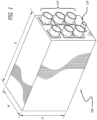
- FIG. 1 is a diagram showing an external view of the disclosed data BiB 100 system design, in accordance with at least one embodiment of the present disclosure.
- the data BiB 100 includes six 5-channel circular 38999 electrical connectors 110 and one 2-channel 38999 POF optical connector 120. It should be noted that in other embodiments, the data BiB 100 may contain more or less than six electrical connectors 110 as shown, and may contain more than one optical connector 120 as shown. In addition, it should be noted that in other embodiments, various different types of electrical connectors 110 other than circular 38999 electrical connectors may be employed by the disclosed data BiB 100. Additionally, it should be noted that in other embodiments, various different types of optical connectors 120 other than circular 38999 optical connectors may be employed by the disclosed data BiB 100.
- the data BiB 100 contains 30 OMCs (25 OMCs plus 5 spare OMCs) (refer to FIG. 2 ), which are housed within a compact 4 MCU sized avionics box 100 with dimensions of 4.88" W x 7.64" H x 12.76" D.
- the box 100 at the same time, achieves high reliability and ruggedness standards that are required by the commercial airplane's avionics environment.
- various sized boxes other than a 4 MCU sized box may be employed for the data BiB 100.
- a 3 MCU sized box may be employed for the data BiB 100.
- Each OMC inside of the data BiB 100 of the POF 629 system bus architecture needs to provide a minimum of a 54 decibels (dB) power budget over an operating temperature range of -40° Celsius (C) to 85°C, and maintain this performance over twenty (20) years of operating life time under stringent avionics environments, which include high vibration, humidity, and contamination.
- dB decibels
- the data BiB box 100 is environmental sealed, before final installation in the airplane, for moisture and contamination prevention. In addition, the data BiB box 100 is ruggedized to withstand mechanical shock and vibration in a commercial airplane environment.
- FIG. 2 is diagram showing an internal view of the disclosed data BiB 200 system design and assembly, in accordance with at least one embodiment of the present disclosure.
- This figure shows the internal three-dimensional (3D) view of 4 MCU sized data BiB 200. Additionally, the figure shows the arrangement and location of thirty (30) OMC PCB tiles 230 on a PCB (e.g., mother board) 240. It should be noted that in other embodiments, the PCB 240 may comprise more or less than 30 OMC PCB tiles 230 as is shown.
- Each OMC tile 230 includes a tilted optical sub-assembly (OSA) 250.
- Each OSA 250 on the OMC tiles 230 is connected to a POF star coupler 260 via a POF 270.
- each POF star coupler 260 is connected to the 2-channel 38999 optical connector via a POF 280.
- each electrical connector 210 connects to five OMCs. And, each electrical connector 210 has twenty (20) electrical pins that are active. It should be noted that in one or more embodiments, each electrical connector 210 may have more or less than 20 electrical pins that are active. The electrical pins are spaced sufficiently apart to minimize cross talk between the active pins.
- thermally conductive foam material 290 is used to fill the space between the center PCB 240 to the wall of the data BiB 200 to enhance thermally conductivity.
- the PCB (e.g., mother board) 240 may comprise a copper core board or a board with an aluminum back plate for enhancement of thermal conductivity.
- FIG. 3 is a diagram showing an internal top view of the disclosed data BiB 200 of FIG. 2 , in accordance with at least one embodiment of the present disclosure.
- OSAs tilted optical sub-assemblies
- POF 285 is shown to be connected from POF star coupler 260a (e.g., a receive coupler) to POF star coupler 260b (e.g., a transmit coupler).
- the arrangement of this layout minimizes the bending of the POF 270a, 270b, 280a, 280b, 285 within the tight space of the data BiB 200.
- the POF 270a, 270b, 280a, 280b, 285 bend radius within the data BiB 200 will not introduce large optical loss due to the bending.
- the POF 270a, 270b, 280a, 280b, 285 and the POF star couplers 260a, 260b are manufactured from a multi-core POF, which has a very high tolerance to tight bending.
- FIG. 4 is a diagram showing an internal side view of the disclosed data BiB 200 of FIG. 2 , in accordance with at least one embodiment of the present disclosure.
- the arrangement of the 30 OMC tiles 230 with the tilted OSAs 250 on the PCB (e.g., mother board) 240 is shown.
- the connection of a POF 270 from a POF star coupler 260 to a tilted OSA 250 shows the POF 270 having a small bend radius.
- the connection of the POF 280 from the POF star coupler 260 to the 2-channel 38999 optical connector 220 is also shown.
- the 38999 electrical connectors 210 are located close to the edge of the PCB (e.g., mother board) 240 to facilitate electrical connections from the connectors 210 to the PCB 240.
- the connections from the PCB 240 to the electrical connectors 210 can be accomplished by employing, for example, a card edge connector or a flexcircuit with a connector to the PCB 240.
- FIG. 5 is a diagram showing an exemplary PCB (e.g., mother board) 240 of the disclosed data BiB 200 of FIG. 2 , in accordance with at least one embodiment of the present disclosure.
- This figure shows a conceptual view of the PCB (e.g., mother board) 240 populated with OMC tiles 230 on one side.
- the PCB 240 is partitioned into an array of OMC tiles 230, with all transmitting tiles 230 (to perform electrical to optical conversion) on one side of the PCB 240 and all receiving tiles 230 (to perform optical to electrical conversion) on the other side of the PCB 240.
- This design allows for ease of routing of POF separately for transmit and receive, a minimization of crosstalk between the transmit and the receive circuitry, and an increase in PCB 240 real estate for other components.
- all of the OMC tiles (i.e. the transmit OMC tiles and the receive OMC tiles) 230 are electrically isolated from each other.
- the remaining OMC tiles 230 are not affected by the failure (i.e. the failed OMC tile 230 does not affect the communication of the remaining OMC tiles 230 on the data bus).
- each OMC PCB tile 230 is 1.2" x 2.2" and, as such, the area on both sides (i.e. the transmit side and the receive side) of each OMC tile 230 is 34.06 square centimeters (5.28 square inches), which provides sufficient space for the OMC electronic elements and the tilted OSA 250.
- the dimensions of the PCB (e.g., mother board) 240 are 7.2" x 11". Since the side dimensions of a 4 MCU sized box are 7.6" x 12.75", the PCB 240 has a margin of 1.75" in depth and 0.4" in height when housed within a 4 MCU sized box.
- the PCB (e.g., mother board) 240 includes a top edge guide rail 292 and a bottom edge guide rail 295, which are both used to secure the PCB 240 inside of the data BiB 200.
- the PCB 240 includes an edge connector 297, which is used to facilitate electrical connections from the PCB 240 to the electrical connectors 210.
- the transmit OMC tiles 230 comprise at least one spare transmit OMC tile 230 and the receive OMC tiles 230 comprise at least one spare receive OMC tile 230.
- the electrical connectors 210 comprise at least one spare electrical connector 210. When at least one of the transmit OMC tiles 230 and/or the receive OMC tiles 230 fails, at least one spare transmit OMC tile 230 and/or at least one space receive OMC tile 230 is connected to at least one spare electrical connector 210.
- FIG. 6 depicts a flow chart depicting the disclosed method 600 for communication using a data BiB (e.g., the data BiB 200 of FIGS. 2 - 5 ), in accordance with at least one embodiment of the present disclosure.
- a data BiB e.g., the data BiB 200 of FIGS. 2 - 5
- at least one first receive signal is sent from at least one optical connector located on one side of the data BiB to the small end of a receive coupler (e.g., a star coupler) 620.
- a receive coupler e.g., a star coupler
- at least one second receive signal is sent from the large end of the receive coupler (e.g., a star coupler) to at least one receive OMC tile located on the receive side of a PCB (e.g., mother board) housed within the data BiB 630.
- a PCB e.g., mother board
- At least one first transmit signal is sent from at least one transmit OMC tile located on the transmit side of the PCB (e.g., mother board) housed within the data BiB to the large end of a transmit coupler (e.g., a star coupler) 640.
- a transmit coupler e.g., a star coupler
- at least one second transmit signal is sent from the small end of the transmit coupler (e.g., a star coupler) to at least one of the optical connectors and to the small end of the receive coupler 650.
- the method 600 ends 660.
Landscapes
- Physics & Mathematics (AREA)
- General Physics & Mathematics (AREA)
- Optics & Photonics (AREA)
- Engineering & Computer Science (AREA)
- Electromagnetism (AREA)
- Signal Processing (AREA)
- Computer Networks & Wireless Communication (AREA)
- Mechanical Engineering (AREA)
- Computing Systems (AREA)
- Optical Couplings Of Light Guides (AREA)
- Light Guides In General And Applications Therefor (AREA)
- Optical Communication System (AREA)
- Small-Scale Networks (AREA)
Applications Claiming Priority (1)
| Application Number | Priority Date | Filing Date | Title |
|---|---|---|---|
| US14/533,865 US9791644B2 (en) | 2014-11-05 | 2014-11-05 | Data bus-in-a-box (BiB) system design and implementation |
Publications (2)
| Publication Number | Publication Date |
|---|---|
| EP3086150A1 EP3086150A1 (en) | 2016-10-26 |
| EP3086150B1 true EP3086150B1 (en) | 2023-05-31 |
Family
ID=54366139
Family Applications (1)
| Application Number | Title | Priority Date | Filing Date |
|---|---|---|---|
| EP15193003.9A Active EP3086150B1 (en) | 2014-11-05 | 2015-11-04 | Data bus-in-a-box (bib) system design and implementation |
Country Status (6)
| Country | Link |
|---|---|
| US (3) | US9791644B2 (https=) |
| EP (1) | EP3086150B1 (https=) |
| JP (1) | JP6483579B2 (https=) |
| CN (1) | CN105572813B (https=) |
| BR (1) | BR102015027733B1 (https=) |
| RU (1) | RU2690032C2 (https=) |
Families Citing this family (11)
| Publication number | Priority date | Publication date | Assignee | Title |
|---|---|---|---|---|
| US11300730B2 (en) * | 2013-07-30 | 2022-04-12 | The Boeing Company | Plastic and glass optical fiber bus network having plural line replaceable units transmitting to a mixing rod |
| US9778419B1 (en) | 2016-06-23 | 2017-10-03 | The Boeing Company | Fiber optical system with fiber end face area relationships |
| US10447423B2 (en) | 2017-11-03 | 2019-10-15 | The Boeing Company | Bidirectional, multi-wavelength gigabit optical fiber network |
| US10574359B2 (en) | 2018-03-20 | 2020-02-25 | The Boeing Company | Single-wavelength bidirectional transceiver with integrated optical fiber coupler |
| US10964835B2 (en) | 2018-08-29 | 2021-03-30 | The Boeing Company | Universal broadband photodetector design and fabrication process |
| TWI706179B (zh) * | 2018-10-01 | 2020-10-01 | 創威光電股份有限公司 | 光次模組及光次模組的帽蓋 |
| US11243365B2 (en) | 2018-11-16 | 2022-02-08 | The Boeing Company | Methods for providing flammability protection for plastic optical fiber |
| US10852494B2 (en) | 2018-12-11 | 2020-12-01 | The Boeing Company | Avionics pluggable active optical connector |
| US10754111B1 (en) * | 2019-04-22 | 2020-08-25 | The Boeing Company | Method for modifying small form factor pluggable transceiver for avionics applications |
| CN115144975A (zh) * | 2021-03-30 | 2022-10-04 | 讯芸电子科技(中山)有限公司 | 具散热结构的光通讯模块 |
| US11906801B2 (en) * | 2021-07-26 | 2024-02-20 | Te Connectivity Solutions Gmbh | Optical receptacle connector for an optical communication system |
Citations (1)
| Publication number | Priority date | Publication date | Assignee | Title |
|---|---|---|---|---|
| US20120027415A1 (en) * | 2010-07-29 | 2012-02-02 | Chan Eric Y | Burst mode optical media converter with fast analog conversion |
Family Cites Families (39)
| Publication number | Priority date | Publication date | Assignee | Title |
|---|---|---|---|---|
| US5109445A (en) | 1980-11-01 | 1992-04-28 | Raychem Corp. | Strained distribution optical fiber communication system |
| NL8102050A (nl) | 1981-04-27 | 1982-11-16 | Philips Nv | Glasvezeldoorvoer in een metalen behuizing. |
| US4545077A (en) * | 1982-10-29 | 1985-10-01 | Lockheed Corporation | Electro-optical data bus |
| US4650276A (en) | 1983-12-21 | 1987-03-17 | Gte Laboratories Incorporated | Optical fiber connected broadband microwave package for optoelectronic components |
| DE3587515T2 (de) | 1984-05-17 | 1994-03-17 | Nippon Electric Co | Optische Schalteinrichtung. |
| JPS6188208A (ja) | 1984-10-08 | 1986-05-06 | Nec Corp | 光フアイバ・コネクタ |
| DE3517389A1 (de) * | 1985-05-14 | 1986-11-20 | Allied Corp., Morristown, N.J. | Kontakt mit auswechselbarem opto-elektronischem element |
| US5002356A (en) | 1989-04-28 | 1991-03-26 | Raynet Corp. | Optical fiber tap handling tray with fiber installation tool |
| US5039194A (en) * | 1990-01-09 | 1991-08-13 | International Business Machines Corporation | Optical fiber link card |
| US5069522A (en) * | 1990-01-09 | 1991-12-03 | International Business Machines Corporation | Optical fiber link card |
| US5165002A (en) | 1991-11-27 | 1992-11-17 | Motorola, Inc. | Method of coupling an electrical signal to an optical fiber |
| JP2833536B2 (ja) * | 1995-09-06 | 1998-12-09 | 日本電気株式会社 | 光バスおよび光バス構成素子 |
| US5926378A (en) * | 1995-09-29 | 1999-07-20 | International Business Machines Corporation | Low profile riser card assembly using paired back-to-back peripheral card connectors mounted on universal footprints supporting different bus form factors |
| DE10040651B4 (de) * | 2000-08-19 | 2004-02-05 | Erni Elektroapparate Gmbh | Elektronisches Gerät mit Daten- und/oder Energiebusverbindung |
| US6631237B2 (en) * | 2001-03-06 | 2003-10-07 | Adc Telecommunications, Inc. | Termination and splice panel |
| US7023705B2 (en) * | 2001-08-03 | 2006-04-04 | National Semiconductor Corporation | Ceramic optical sub-assembly for optoelectronic modules |
| CN2626161Y (zh) * | 2003-04-28 | 2004-07-14 | 华为技术有限公司 | 一种双面插背板 |
| JP2005037642A (ja) * | 2003-07-14 | 2005-02-10 | Nippon Telegr & Teleph Corp <Ntt> | 多チャネル光モジュール |
| US6982437B2 (en) | 2003-09-19 | 2006-01-03 | Agilent Technologies, Inc. | Surface emitting laser package having integrated optical element and alignment post |
| US7518883B1 (en) * | 2003-10-09 | 2009-04-14 | Nortel Networks Limited | Backplane architecture for enabling configuration of multi-service network elements for use in a global variety of communications networks |
| NL1026832C2 (nl) | 2004-08-12 | 2006-02-14 | Genexis B V | Inrichting voor het aansluiten van apparaten op lichtgeleidende vezels. |
| US7373031B2 (en) * | 2004-09-30 | 2008-05-13 | Intel Corporation | Apparatus for an electro-optical device connection |
| US7660128B2 (en) * | 2004-09-30 | 2010-02-09 | Emcore Corporation | Apparatus for electrical and optical interconnection |
| US7751717B2 (en) * | 2004-12-30 | 2010-07-06 | Finisar Corporation | Host printed circuit board with multiple optical transceivers |
| JP2006262564A (ja) * | 2005-03-15 | 2006-09-28 | Nippon Telegr & Teleph Corp <Ntt> | 光電変換アウトレット |
| US7359592B2 (en) * | 2006-03-21 | 2008-04-15 | The Boeing Company | Single fiber links for full duplex aircraft data network |
| JP5017959B2 (ja) * | 2006-08-14 | 2012-09-05 | 富士通オプティカルコンポーネンツ株式会社 | 偏光無依存型光アイソレータ及び光送受信装置 |
| US7817438B2 (en) * | 2006-12-21 | 2010-10-19 | Asia Optical Co., Inc. | Transceiver module and PCB structure thereof |
| US8045858B2 (en) * | 2008-07-24 | 2011-10-25 | The Boeing Company | Methods and systems for providing full avionics data services over a single fiber |
| US8320766B2 (en) * | 2009-01-20 | 2012-11-27 | The Boeing Company | Inline optoelectronic converter and associated methods |
| US9077451B2 (en) * | 2009-01-20 | 2015-07-07 | The Boeing Company | Inline optoelectronic converter and associated methods |
| US8983302B2 (en) * | 2009-11-05 | 2015-03-17 | The Boeing Company | Transceiver for plastic optical fiber networks |
| US8521032B2 (en) * | 2010-04-01 | 2013-08-27 | The Boeing Company | Optical fiber interface system and connector |
| CN102436045A (zh) | 2011-12-29 | 2012-05-02 | 武汉电信器件有限公司 | 一种光电子器件的光导纤维的安装固定结构 |
| US9235018B2 (en) | 2012-05-30 | 2016-01-12 | Avago Technologies General Ip (Singapore) Pte. Ltd. | Optical communications card, an optical communications system, and methods and apparatuses for providing high-density mounting of optical communications cards |
| US9276335B2 (en) * | 2012-12-11 | 2016-03-01 | Advanced Micro Devices, Inc. | Double-sided circuit board with opposing modular card connector assemblies |
| TWM484713U (zh) * | 2014-03-10 | 2014-08-21 | Luxnet Corp | 可替換式光發射模組及搭載有可替換式光發射模組的光收發器 |
| US9513677B2 (en) * | 2014-03-18 | 2016-12-06 | Western Digital Technologies, Inc. | Shaped backplane for receiving electrical components |
| US9071357B1 (en) * | 2014-07-11 | 2015-06-30 | Emcore Corporation | Data communications system including an optical fiber data link disposed between serial bidirectional electrical data busses |
-
2014
- 2014-11-05 US US14/533,865 patent/US9791644B2/en active Active
- 2014-11-05 US US14/533,715 patent/US9297970B1/en active Active
-
2015
- 2015-09-16 RU RU2015139367A patent/RU2690032C2/ru active
- 2015-09-18 JP JP2015185138A patent/JP6483579B2/ja active Active
- 2015-11-03 BR BR102015027733-4A patent/BR102015027733B1/pt active IP Right Grant
- 2015-11-03 CN CN201510737785.5A patent/CN105572813B/zh active Active
- 2015-11-04 EP EP15193003.9A patent/EP3086150B1/en active Active
-
2016
- 2016-03-04 US US15/061,879 patent/US9851518B2/en active Active
Patent Citations (1)
| Publication number | Priority date | Publication date | Assignee | Title |
|---|---|---|---|---|
| US20120027415A1 (en) * | 2010-07-29 | 2012-02-02 | Chan Eric Y | Burst mode optical media converter with fast analog conversion |
Also Published As
| Publication number | Publication date |
|---|---|
| JP2016091010A (ja) | 2016-05-23 |
| CN105572813B (zh) | 2019-03-29 |
| RU2690032C2 (ru) | 2019-05-30 |
| RU2015139367A3 (https=) | 2019-03-22 |
| BR102015027733A2 (pt) | 2016-05-24 |
| BR102015027733B1 (pt) | 2023-01-10 |
| US9851518B2 (en) | 2017-12-26 |
| US9297970B1 (en) | 2016-03-29 |
| US20160187598A1 (en) | 2016-06-30 |
| CN105572813A (zh) | 2016-05-11 |
| JP6483579B2 (ja) | 2019-03-13 |
| RU2015139367A (ru) | 2017-03-21 |
| US20160124169A1 (en) | 2016-05-05 |
| US9791644B2 (en) | 2017-10-17 |
| EP3086150A1 (en) | 2016-10-26 |
Similar Documents
| Publication | Publication Date | Title |
|---|---|---|
| EP3086150B1 (en) | Data bus-in-a-box (bib) system design and implementation | |
| US12490401B2 (en) | Data processing systems including optical communication modules | |
| US20230375793A1 (en) | Communication systems having pluggable modules | |
| US20230176304A1 (en) | Communication systems having pluggable modules | |
| US7452236B2 (en) | Cabling for rack-mount devices | |
| US10725245B2 (en) | High-density fabric systems interconnected with multi-port aggregated cables | |
| US7120327B2 (en) | Backplane assembly with board to board optical interconnections | |
| US20240302612A1 (en) | Communication systems having pluggable modules | |
| US8417071B2 (en) | Data storage system, a modular printed circuit board, a backplane and a backplane component | |
| RU2691643C2 (ru) | Малозатратные, бессоединительные, обладающие повышенной прочностью и малым форм-фактором оптический подузел (osa) и одноконтейнерная шина (bib) данных | |
| CN113810120A (zh) | 提高安全的可插拔激光模块 | |
| WO1994002973A1 (en) | Apparatus for connecting computer devices | |
| CN108023641A (zh) | 一种柔性光纤网络互连方法及应用该方法的综合核心处理机 | |
| US10502910B2 (en) | Transceiver modules | |
| US10623101B1 (en) | Hyperscale photonics connectivity solution | |
| US10791385B2 (en) | Optical to electrical conversion module | |
| CN104604246A (zh) | 用于光学互连的电信系统的拓扑定义卡 | |
| CA2814108C (en) | Telecommunications equipment | |
| CN112399175B (zh) | 一种arinc818子卡的试验平台 | |
| WO2012015384A1 (en) | A system including a module | |
| WO2023093105A1 (zh) | 一种光背板互连装置及通信设备 | |
| Weaver et al. | Photonic Exchange Network: a reconfigurable data network for mobile platforms | |
| Schroeder et al. | Optical interconnection and packaging technologies for advanced avionics systems | |
| Ellis et al. | Fiber Optics Application To A-7 Aircraft |
Legal Events
| Date | Code | Title | Description |
|---|---|---|---|
| PUAI | Public reference made under article 153(3) epc to a published international application that has entered the european phase |
Free format text: ORIGINAL CODE: 0009012 |
|
| 17P | Request for examination filed |
Effective date: 20151104 |
|
| AK | Designated contracting states |
Kind code of ref document: A1 Designated state(s): AL AT BE BG CH CY CZ DE DK EE ES FI FR GB GR HR HU IE IS IT LI LT LU LV MC MK MT NL NO PL PT RO RS SE SI SK SM TR |
|
| AX | Request for extension of the european patent |
Extension state: BA ME |
|
| STAA | Information on the status of an ep patent application or granted ep patent |
Free format text: STATUS: EXAMINATION IS IN PROGRESS |
|
| 17Q | First examination report despatched |
Effective date: 20200513 |
|
| RIC1 | Information provided on ipc code assigned before grant |
Ipc: H04B 10/40 20130101ALI20220511BHEP Ipc: G02B 6/38 20060101ALI20220511BHEP Ipc: G02B 6/44 20060101AFI20220511BHEP |
|
| GRAP | Despatch of communication of intention to grant a patent |
Free format text: ORIGINAL CODE: EPIDOSNIGR1 |
|
| STAA | Information on the status of an ep patent application or granted ep patent |
Free format text: STATUS: GRANT OF PATENT IS INTENDED |
|
| INTG | Intention to grant announced |
Effective date: 20220817 |
|
| GRAS | Grant fee paid |
Free format text: ORIGINAL CODE: EPIDOSNIGR3 |
|
| GRAJ | Information related to disapproval of communication of intention to grant by the applicant or resumption of examination proceedings by the epo deleted |
Free format text: ORIGINAL CODE: EPIDOSDIGR1 |
|
| GRAL | Information related to payment of fee for publishing/printing deleted |
Free format text: ORIGINAL CODE: EPIDOSDIGR3 |
|
| STAA | Information on the status of an ep patent application or granted ep patent |
Free format text: STATUS: EXAMINATION IS IN PROGRESS |
|
| INTC | Intention to grant announced (deleted) | ||
| GRAP | Despatch of communication of intention to grant a patent |
Free format text: ORIGINAL CODE: EPIDOSNIGR1 |
|
| STAA | Information on the status of an ep patent application or granted ep patent |
Free format text: STATUS: GRANT OF PATENT IS INTENDED |
|
| RAP3 | Party data changed (applicant data changed or rights of an application transferred) |
Owner name: THE BOEING COMPANY |
|
| INTG | Intention to grant announced |
Effective date: 20230315 |
|
| GRAA | (expected) grant |
Free format text: ORIGINAL CODE: 0009210 |
|
| STAA | Information on the status of an ep patent application or granted ep patent |
Free format text: STATUS: THE PATENT HAS BEEN GRANTED |
|
| AK | Designated contracting states |
Kind code of ref document: B1 Designated state(s): AL AT BE BG CH CY CZ DE DK EE ES FI FR GB GR HR HU IE IS IT LI LT LU LV MC MK MT NL NO PL PT RO RS SE SI SK SM TR |
|
| REG | Reference to a national code |
Ref country code: GB Ref legal event code: FG4D Ref country code: CH Ref legal event code: EP |
|
| REG | Reference to a national code |
Ref country code: DE Ref legal event code: R096 Ref document number: 602015083729 Country of ref document: DE |
|
| REG | Reference to a national code |
Ref country code: AT Ref legal event code: REF Ref document number: 1571264 Country of ref document: AT Kind code of ref document: T Effective date: 20230615 |
|
| REG | Reference to a national code |
Ref country code: IE Ref legal event code: FG4D |
|
| P01 | Opt-out of the competence of the unified patent court (upc) registered |
Effective date: 20230526 |
|
| REG | Reference to a national code |
Ref country code: LT Ref legal event code: MG9D |
|
| REG | Reference to a national code |
Ref country code: NL Ref legal event code: MP Effective date: 20230531 |
|
| REG | Reference to a national code |
Ref country code: AT Ref legal event code: MK05 Ref document number: 1571264 Country of ref document: AT Kind code of ref document: T Effective date: 20230531 |
|
| PG25 | Lapsed in a contracting state [announced via postgrant information from national office to epo] |
Ref country code: SE Free format text: LAPSE BECAUSE OF FAILURE TO SUBMIT A TRANSLATION OF THE DESCRIPTION OR TO PAY THE FEE WITHIN THE PRESCRIBED TIME-LIMIT Effective date: 20230531 Ref country code: NO Free format text: LAPSE BECAUSE OF FAILURE TO SUBMIT A TRANSLATION OF THE DESCRIPTION OR TO PAY THE FEE WITHIN THE PRESCRIBED TIME-LIMIT Effective date: 20230831 Ref country code: ES Free format text: LAPSE BECAUSE OF FAILURE TO SUBMIT A TRANSLATION OF THE DESCRIPTION OR TO PAY THE FEE WITHIN THE PRESCRIBED TIME-LIMIT Effective date: 20230531 Ref country code: AT Free format text: LAPSE BECAUSE OF FAILURE TO SUBMIT A TRANSLATION OF THE DESCRIPTION OR TO PAY THE FEE WITHIN THE PRESCRIBED TIME-LIMIT Effective date: 20230531 |
|
| PG25 | Lapsed in a contracting state [announced via postgrant information from national office to epo] |
Ref country code: RS Free format text: LAPSE BECAUSE OF FAILURE TO SUBMIT A TRANSLATION OF THE DESCRIPTION OR TO PAY THE FEE WITHIN THE PRESCRIBED TIME-LIMIT Effective date: 20230531 Ref country code: PL Free format text: LAPSE BECAUSE OF FAILURE TO SUBMIT A TRANSLATION OF THE DESCRIPTION OR TO PAY THE FEE WITHIN THE PRESCRIBED TIME-LIMIT Effective date: 20230531 Ref country code: NL Free format text: LAPSE BECAUSE OF FAILURE TO SUBMIT A TRANSLATION OF THE DESCRIPTION OR TO PAY THE FEE WITHIN THE PRESCRIBED TIME-LIMIT Effective date: 20230531 Ref country code: LV Free format text: LAPSE BECAUSE OF FAILURE TO SUBMIT A TRANSLATION OF THE DESCRIPTION OR TO PAY THE FEE WITHIN THE PRESCRIBED TIME-LIMIT Effective date: 20230531 Ref country code: LT Free format text: LAPSE BECAUSE OF FAILURE TO SUBMIT A TRANSLATION OF THE DESCRIPTION OR TO PAY THE FEE WITHIN THE PRESCRIBED TIME-LIMIT Effective date: 20230531 Ref country code: IS Free format text: LAPSE BECAUSE OF FAILURE TO SUBMIT A TRANSLATION OF THE DESCRIPTION OR TO PAY THE FEE WITHIN THE PRESCRIBED TIME-LIMIT Effective date: 20230930 Ref country code: HR Free format text: LAPSE BECAUSE OF FAILURE TO SUBMIT A TRANSLATION OF THE DESCRIPTION OR TO PAY THE FEE WITHIN THE PRESCRIBED TIME-LIMIT Effective date: 20230531 Ref country code: GR Free format text: LAPSE BECAUSE OF FAILURE TO SUBMIT A TRANSLATION OF THE DESCRIPTION OR TO PAY THE FEE WITHIN THE PRESCRIBED TIME-LIMIT Effective date: 20230901 |
|
| PG25 | Lapsed in a contracting state [announced via postgrant information from national office to epo] |
Ref country code: FI Free format text: LAPSE BECAUSE OF FAILURE TO SUBMIT A TRANSLATION OF THE DESCRIPTION OR TO PAY THE FEE WITHIN THE PRESCRIBED TIME-LIMIT Effective date: 20230531 |
|
| PG25 | Lapsed in a contracting state [announced via postgrant information from national office to epo] |
Ref country code: SK Free format text: LAPSE BECAUSE OF FAILURE TO SUBMIT A TRANSLATION OF THE DESCRIPTION OR TO PAY THE FEE WITHIN THE PRESCRIBED TIME-LIMIT Effective date: 20230531 |
|
| PG25 | Lapsed in a contracting state [announced via postgrant information from national office to epo] |
Ref country code: SM Free format text: LAPSE BECAUSE OF FAILURE TO SUBMIT A TRANSLATION OF THE DESCRIPTION OR TO PAY THE FEE WITHIN THE PRESCRIBED TIME-LIMIT Effective date: 20230531 Ref country code: SK Free format text: LAPSE BECAUSE OF FAILURE TO SUBMIT A TRANSLATION OF THE DESCRIPTION OR TO PAY THE FEE WITHIN THE PRESCRIBED TIME-LIMIT Effective date: 20230531 Ref country code: RO Free format text: LAPSE BECAUSE OF FAILURE TO SUBMIT A TRANSLATION OF THE DESCRIPTION OR TO PAY THE FEE WITHIN THE PRESCRIBED TIME-LIMIT Effective date: 20230531 Ref country code: PT Free format text: LAPSE BECAUSE OF FAILURE TO SUBMIT A TRANSLATION OF THE DESCRIPTION OR TO PAY THE FEE WITHIN THE PRESCRIBED TIME-LIMIT Effective date: 20231002 Ref country code: EE Free format text: LAPSE BECAUSE OF FAILURE TO SUBMIT A TRANSLATION OF THE DESCRIPTION OR TO PAY THE FEE WITHIN THE PRESCRIBED TIME-LIMIT Effective date: 20230531 Ref country code: DK Free format text: LAPSE BECAUSE OF FAILURE TO SUBMIT A TRANSLATION OF THE DESCRIPTION OR TO PAY THE FEE WITHIN THE PRESCRIBED TIME-LIMIT Effective date: 20230531 Ref country code: CZ Free format text: LAPSE BECAUSE OF FAILURE TO SUBMIT A TRANSLATION OF THE DESCRIPTION OR TO PAY THE FEE WITHIN THE PRESCRIBED TIME-LIMIT Effective date: 20230531 |
|
| REG | Reference to a national code |
Ref country code: DE Ref legal event code: R097 Ref document number: 602015083729 Country of ref document: DE |
|
| PLBE | No opposition filed within time limit |
Free format text: ORIGINAL CODE: 0009261 |
|
| STAA | Information on the status of an ep patent application or granted ep patent |
Free format text: STATUS: NO OPPOSITION FILED WITHIN TIME LIMIT |
|
| PG25 | Lapsed in a contracting state [announced via postgrant information from national office to epo] |
Ref country code: SI Free format text: LAPSE BECAUSE OF FAILURE TO SUBMIT A TRANSLATION OF THE DESCRIPTION OR TO PAY THE FEE WITHIN THE PRESCRIBED TIME-LIMIT Effective date: 20230531 |
|
| 26N | No opposition filed |
Effective date: 20240301 |
|
| PG25 | Lapsed in a contracting state [announced via postgrant information from national office to epo] |
Ref country code: SI Free format text: LAPSE BECAUSE OF FAILURE TO SUBMIT A TRANSLATION OF THE DESCRIPTION OR TO PAY THE FEE WITHIN THE PRESCRIBED TIME-LIMIT Effective date: 20230531 Ref country code: IT Free format text: LAPSE BECAUSE OF FAILURE TO SUBMIT A TRANSLATION OF THE DESCRIPTION OR TO PAY THE FEE WITHIN THE PRESCRIBED TIME-LIMIT Effective date: 20230531 |
|
| REG | Reference to a national code |
Ref country code: CH Ref legal event code: PL |
|
| PG25 | Lapsed in a contracting state [announced via postgrant information from national office to epo] |
Ref country code: MC Free format text: LAPSE BECAUSE OF FAILURE TO SUBMIT A TRANSLATION OF THE DESCRIPTION OR TO PAY THE FEE WITHIN THE PRESCRIBED TIME-LIMIT Effective date: 20230531 |
|
| PG25 | Lapsed in a contracting state [announced via postgrant information from national office to epo] |
Ref country code: LU Free format text: LAPSE BECAUSE OF NON-PAYMENT OF DUE FEES Effective date: 20231104 |
|
| PG25 | Lapsed in a contracting state [announced via postgrant information from national office to epo] |
Ref country code: CH Free format text: LAPSE BECAUSE OF NON-PAYMENT OF DUE FEES Effective date: 20231130 |
|
| PG25 | Lapsed in a contracting state [announced via postgrant information from national office to epo] |
Ref country code: MC Free format text: LAPSE BECAUSE OF FAILURE TO SUBMIT A TRANSLATION OF THE DESCRIPTION OR TO PAY THE FEE WITHIN THE PRESCRIBED TIME-LIMIT Effective date: 20230531 Ref country code: LU Free format text: LAPSE BECAUSE OF NON-PAYMENT OF DUE FEES Effective date: 20231104 Ref country code: CH Free format text: LAPSE BECAUSE OF NON-PAYMENT OF DUE FEES Effective date: 20231130 |
|
| REG | Reference to a national code |
Ref country code: BE Ref legal event code: MM Effective date: 20231130 |
|
| REG | Reference to a national code |
Ref country code: IE Ref legal event code: MM4A |
|
| PG25 | Lapsed in a contracting state [announced via postgrant information from national office to epo] |
Ref country code: IE Free format text: LAPSE BECAUSE OF NON-PAYMENT OF DUE FEES Effective date: 20231104 |
|
| PG25 | Lapsed in a contracting state [announced via postgrant information from national office to epo] |
Ref country code: BE Free format text: LAPSE BECAUSE OF NON-PAYMENT OF DUE FEES Effective date: 20231130 |
|
| PG25 | Lapsed in a contracting state [announced via postgrant information from national office to epo] |
Ref country code: IE Free format text: LAPSE BECAUSE OF NON-PAYMENT OF DUE FEES Effective date: 20231104 Ref country code: BE Free format text: LAPSE BECAUSE OF NON-PAYMENT OF DUE FEES Effective date: 20231130 |
|
| PG25 | Lapsed in a contracting state [announced via postgrant information from national office to epo] |
Ref country code: BG Free format text: LAPSE BECAUSE OF FAILURE TO SUBMIT A TRANSLATION OF THE DESCRIPTION OR TO PAY THE FEE WITHIN THE PRESCRIBED TIME-LIMIT Effective date: 20230531 |
|
| PG25 | Lapsed in a contracting state [announced via postgrant information from national office to epo] |
Ref country code: BG Free format text: LAPSE BECAUSE OF FAILURE TO SUBMIT A TRANSLATION OF THE DESCRIPTION OR TO PAY THE FEE WITHIN THE PRESCRIBED TIME-LIMIT Effective date: 20230531 |
|
| PG25 | Lapsed in a contracting state [announced via postgrant information from national office to epo] |
Ref country code: CY Free format text: LAPSE BECAUSE OF FAILURE TO SUBMIT A TRANSLATION OF THE DESCRIPTION OR TO PAY THE FEE WITHIN THE PRESCRIBED TIME-LIMIT; INVALID AB INITIO Effective date: 20151104 |
|
| PG25 | Lapsed in a contracting state [announced via postgrant information from national office to epo] |
Ref country code: HU Free format text: LAPSE BECAUSE OF FAILURE TO SUBMIT A TRANSLATION OF THE DESCRIPTION OR TO PAY THE FEE WITHIN THE PRESCRIBED TIME-LIMIT; INVALID AB INITIO Effective date: 20151104 |
|
| PG25 | Lapsed in a contracting state [announced via postgrant information from national office to epo] |
Ref country code: TR Free format text: LAPSE BECAUSE OF FAILURE TO SUBMIT A TRANSLATION OF THE DESCRIPTION OR TO PAY THE FEE WITHIN THE PRESCRIBED TIME-LIMIT Effective date: 20230531 |
|
| PGFP | Annual fee paid to national office [announced via postgrant information from national office to epo] |
Ref country code: DE Payment date: 20251128 Year of fee payment: 11 |
|
| PGFP | Annual fee paid to national office [announced via postgrant information from national office to epo] |
Ref country code: GB Payment date: 20251127 Year of fee payment: 11 |
|
| PGFP | Annual fee paid to national office [announced via postgrant information from national office to epo] |
Ref country code: FR Payment date: 20251125 Year of fee payment: 11 |